Embed Size (px)
Citation preview
〇Product structure : Silicon monolithic integrated circuit 〇This product has no designed protection against radioactive rays .
1/26© 2017 ROHM Co., Ltd. All rights reserved. TSZ22111 • 14 • 001
www.rohm.com TSZ02201-0H1H0B102060-1-204.Oct.2017 Rev.001
DC Brushless Fan Motor Drivers
Multifunction Single-phase Full-wave Fan Motor Driver BD61246EFV
General Description BD61246EFV is a 1chip driver that is composed of H-bridge power DMOS FET. Moreover, the circuitconfiguration is restructured, and convenience has beenimproved by reducing the external parts and simplifyingthe setting compared with the conventional driver.The pin is compatible with BD61245EFV (Rotationspeed pulse signal output).
Features High Heat Radiation Package Driver Including Power DMOS FET Speed Controllable by DC / PWM Input I/O Duty Slope Adjust PWM Soft Switching Current Limit Start Duty Assist Lock Protection and Automatic Restart Quick Start Lock Alarm Signal (AL) Output
Key Specifications Operating Voltage Range: 4V to 16V Operating Temperature Range: –40°C to +105°C Output Voltage(total): 0.2V(Typ) at 0.4A
Package W (Typ) x D (Typ) x H (Max) HTSSOP-B16 5.00mm x 6.40mm x 1.00mm
Applications Fan motors for general consumer equipment of desktop PC, Projector, etc.
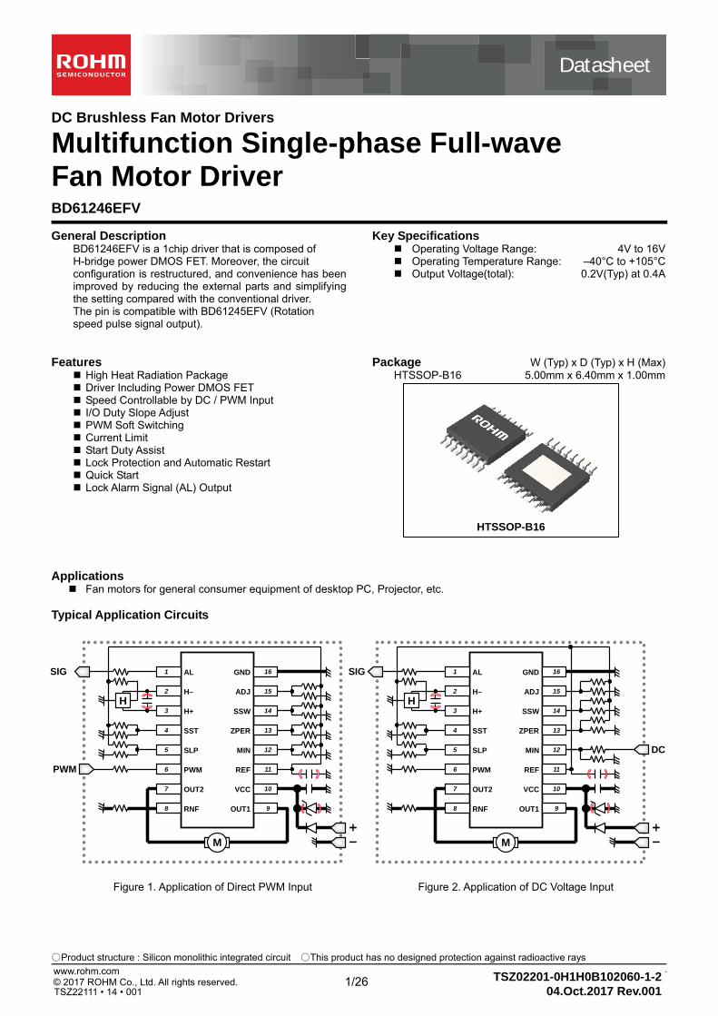
Typical Application Circuits
HTSSOP-B16
Figure 1. Application of Direct PWM Input Figure 2. Application of DC Voltage Input
+
PWM
-M
H
SST
OUT2
H+
H–
OUT1
VCC
MIN
ZPER
ADJ
REF
RNF
SSW
PWM
SIG AL 1 GND
SLP
2
3
15
14
13
12
4
5
6
7
8
11
10
9
16
+
DC
-M
H
SST
OUT2
H+
H–
OUT1
VCC
MIN
ZPER
ADJ
REF
RNF
SSW
PWM
SIG AL 1 GND
SLP
2
3
15
14
13
12
4
5
6
7
8
11
10
9
16
Datasheet
DatasheetDatasheet
.
2/26 © 2017 ROHM Co., Ltd. All rights reserved. TSZ22111 • 15 • 001
www.rohm.com
BD61246EFV
TSZ02201-0H1H0B102060-1-2 04.Oct.2017 Rev.001
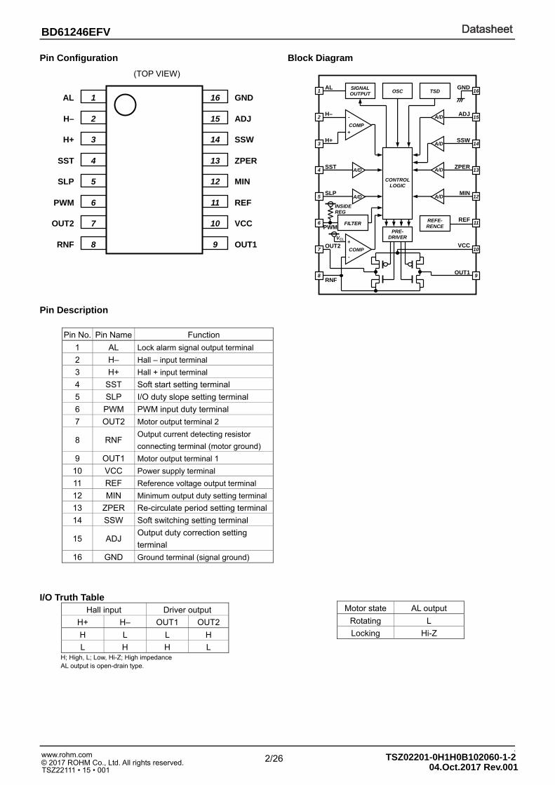
Pin Configuration Pin Description
I/O Truth Table
Hall input Driver output
H+ H– OUT1 OUT2
H L L H
L H H L H; High, L; Low, Hi-Z; High impedance AL output is open-drain type.
Block Diagram
Pin No. Pin Name Function
1 AL Lock alarm signal output terminal
2 H– Hall – input terminal
3 H+ Hall + input terminal
4 SST Soft start setting terminal
5 SLP I/O duty slope setting terminal
6 PWM PWM input duty terminal
7 OUT2 Motor output terminal 2
8 RNF Output current detecting resistor
connecting terminal (motor ground)
9 OUT1 Motor output terminal 1
10 VCC Power supply terminal
11 REF Reference voltage output terminal
12 MIN Minimum output duty setting terminal
13 ZPER Re-circulate period setting terminal
14 SSW Soft switching setting terminal
15 ADJ Output duty correction setting
terminal
16 GND Ground terminal (signal ground)
Motor state AL output
Rotating L
Locking Hi-Z
(TOP VIEW)
SSW
MIN
H+
OUT2
SST
H–
AL
VCC
REF
ADJ
SLP
GND
ZPER
RNF
1
2
3
4
5
6
7
15
OUT1
PWM
16
8
14
13
12
11
9
10
SST
OUT2
H+
H–
OUT1
VCC
MIN
ZPER
ADJ
TSD
CONTROL LOGIC
OSC
FILTER REF REFE-
RENCE
RNF
PRE- DRIVER
SSW
PWM
INSIDE REG
15
14
13
12
2
3
4
5
6
7
8
11
10
9
AL SIGNAL OUTPUT
1 GND
16
+
-
COMP
COMP
+
-
VCL
SLP
A/D
A/D A/D
A/D
A/D
A/D
DatasheetDatasheet
.
3/26 © 2017 ROHM Co., Ltd. All rights reserved. TSZ22111 • 15 • 001
www.rohm.com
BD61246EFV
TSZ02201-0H1H0B102060-1-2 04.Oct.2017 Rev.001
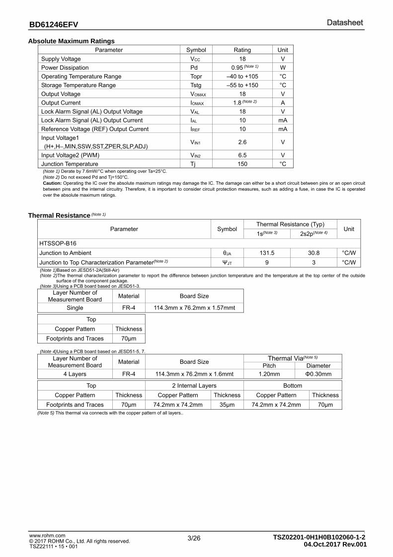
Absolute Maximum Ratings Parameter Symbol Rating Unit
Supply Voltage VCC 18 V
Power Dissipation Pd 0.95 (Note 1) W
Operating Temperature Range Topr –40 to +105 °C
Storage Temperature Range Tstg –55 to +150 °C
Output Voltage VOMAX 18 V
Output Current IOMAX 1.8 (Note 2) A
Lock Alarm Signal (AL) Output Voltage VAL 18 V
Lock Alarm Signal (AL) Output Current IAL 10 mA
Reference Voltage (REF) Output Current IREF 10 mA
Input Voltage1
(H+,H–,MIN,SSW,SST,ZPER,SLP,ADJ) VIN1 2.6 V
Input Voltage2 (PWM) VIN2 6.5 V
Junction Temperature Tj 150 °C (Note 1) Derate by 7.6mW/°C when operating over Ta=25°C. (Note 2) Do not exceed Pd and Tj=150°C. Caution: Operating the IC over the absolute maximum ratings may damage the IC. The damage can either be a short circuit between pins or an open circuit between pins and the internal circuitry. Therefore, it is important to consider circuit protection measures, such as adding a fuse, in case the IC is operated over the absolute maximum ratings.
Thermal Resistance (Note 1)
Parameter Symbol Thermal Resistance (Typ)
Unit 1s(Note 3) 2s2p(Note 4)
HTSSOP-B16
Junction to Ambient θJA 131.5 30.8 °C/W
Junction to Top Characterization Parameter(Note 2) ΨJT 9 3 °C/W (Note 1)Based on JESD51-2A(Still-Air) (Note 2)The thermal characterization parameter to report the difference between junction temperature and the temperature at the top center of the outside
surface of the component package. (Note 3)Using a PCB board based on JESD51-3.
Layer Number of Measurement Board
Material Board Size
Single FR-4 114.3mm x 76.2mm x 1.57mmt
Top
Copper Pattern Thickness
Footprints and Traces 70μm
(Note 4)Using a PCB board based on JESD51-5, 7.
Layer Number of Measurement Board
Material Board Size Thermal Via(Note 5) Pitch Diameter
4 Layers FR-4 114.3mm x 76.2mm x 1.6mmt 1.20mm Φ0.30mm
Top 2 Internal Layers Bottom
Copper Pattern Thickness Copper Pattern Thickness Copper Pattern Thickness
Footprints and Traces 70μm 74.2mm x 74.2mm 35μm 74.2mm x 74.2mm 70μm (Note 5) This thermal via connects with the copper pattern of all layers..
DatasheetDatasheet
.
4/26 © 2017 ROHM Co., Ltd. All rights reserved. TSZ22111 • 15 • 001
www.rohm.com
BD61246EFV
TSZ02201-0H1H0B102060-1-2 04.Oct.2017 Rev.001
Recommended Operating Conditions
Parameter Symbol Min Typ Max Unit
Operating Supply Voltage VCC 4 12 16 V
Hall Input Voltage VH 0 - 2 V
PWM Input Frequency fPWM 15 - 50 kHz Electrical Characteristics (Unless otherwise specified Ta=25°C, VCC=12V)
Parameter Symbol Limit
Unit Conditions Characteristic
Data Min Typ Max
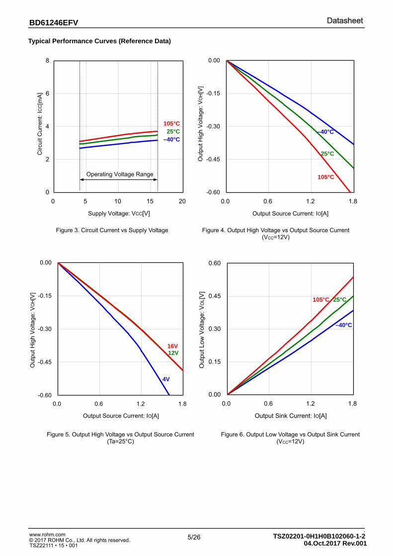
Circuit Current ICC 1.8 3.3 4.8 mA Figure 3
Output Voltage VO - 0.2 0.44 V IO=±400mA,
High and low side total
Figure 4 to
Figure 7
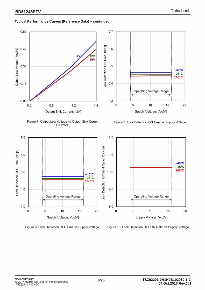
Lock Detection ON Time tON 0.3 0.5 0.7 s Figure 8
Lock Detection OFF Time tOFF 3.0 5.0 7.0 s Figure 9
Lock Detection OFF/ON Ratio rLCK 8 10 12 - rLCK=tOFF / tON Figure 10
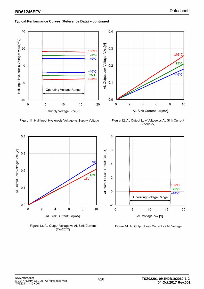
Hall Input Hysteresis Voltage VHYS+ ±7 ±12 ±17 mV Figure 11
AL Output Low Voltage VALL - - 0.3 V IAL=5mA Figure 12 to
Figure 13
AL Output Leak Current IALL - - 10 μA VAL=16V Figure 14
PWM Input High Level Voltage VPWMH 2.5 - 5.0 V -
PWM Input Low Level Voltage VPWML -0.3 - 1.0 V -
PWM Input Current IPWMH -10 0 10 μA VPWM=5V Figure 15 to
Figure 16 IPWML -50 -25 -12 μA VPWM=0V
Reference Voltage VREF 2.2 2.4 2.6 V IREF=-1mA Figure 17 to
Figure 18
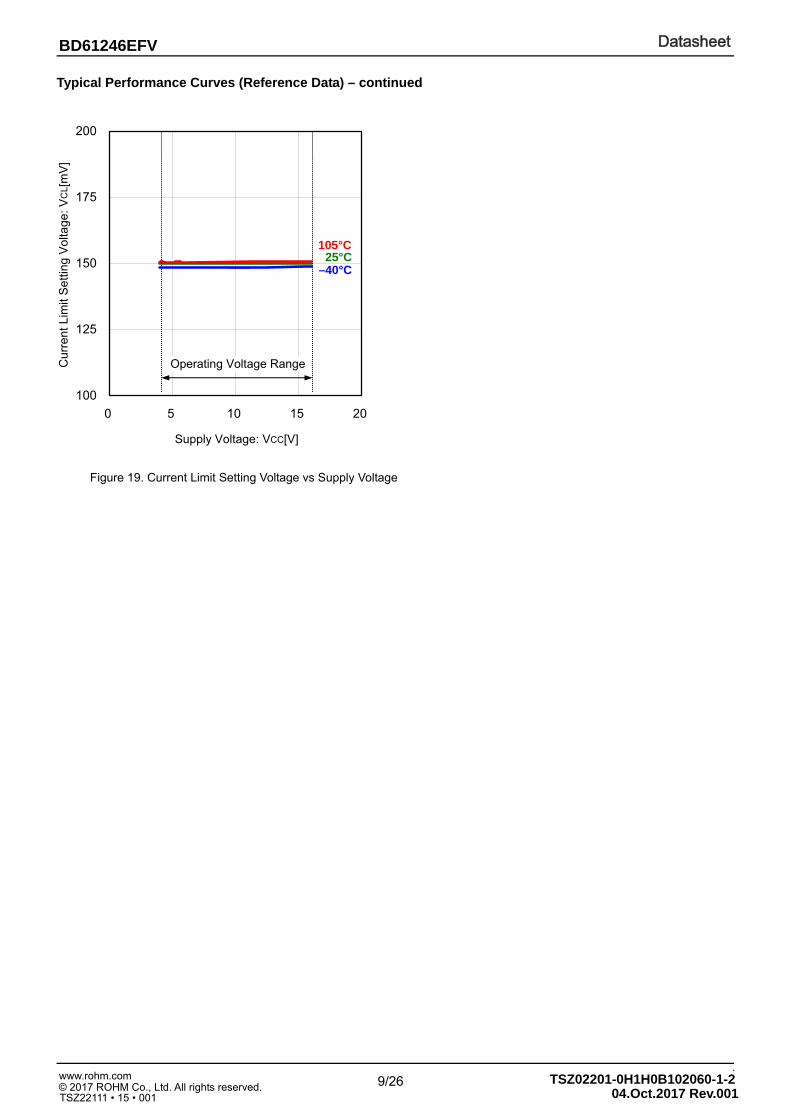
Current Limit Setting Voltage VCL 120 150 180 mV Figure 19 For parameters involving current, positive notation means inflow of current to IC while negative notation means outflow of current from IC.
DatasheetDatasheet
.
5/26 © 2017 ROHM Co., Ltd. All rights reserved. TSZ22111 • 15 • 001
www.rohm.com
BD61246EFV
TSZ02201-0H1H0B102060-1-2 04.Oct.2017 Rev.001
Typical Performance Curves (Reference Data)
Figure 4. Output High Voltage vs Output Source Current (VCC=12V)
Figure 3. Circuit Current vs Supply Voltage
Figure 6. Output Low Voltage vs Output Sink Current (VCC=12V)
0
2
4
6
8
0 5 10 15 20
Supply Voltage: VCC[V]
Cir
cuit
Cu
rre
nt:
IC
C[m
A]
105°C 25°C
–40°C
Operating Voltage Range
Figure 5. Output High Voltage vs Output Source Current (Ta=25°C)
-0.60
-0.45
-0.30
-0.15
0.00
0.0 0.6 1.2 1.8
Output Source Current: IO[A]
Ou
tpu
t H
igh
Vol
tag
e:
VO
H[V
]
105°C
25°C
–40°C
-0.60
-0.45
-0.30
-0.15
0.00
0.0 0.6 1.2 1.8
Output Source Current: IO[A]
Ou
tpu
t H
igh
Vo
ltag
e:
VO
H[V
]
16V 12V
4V
0.00
0.15
0.30
0.45
0.60
0.0 0.6 1.2 1.8
Output Sink Current: IO[A]
Out
put
Low
Vol
tage
: V
OL[
V]
105°C 25°C
–40°C
DatasheetDatasheet
.
6/26 © 2017 ROHM Co., Ltd. All rights reserved. TSZ22111 • 15 • 001
www.rohm.com
BD61246EFV
TSZ02201-0H1H0B102060-1-2 04.Oct.2017 Rev.001
Typical Performance Curves (Reference Data) – continued
8.0
9.0
10.0
11.0
12.0
0 5 10 15 20
Supply Voltage: Vcc[V]
Lo
ck D
ete
ctio
n O
FF
/ON
Ra
tio: R
LCK[s
/s]
105°C 25°C
–40°C
0.3
0.4
0.5
0.6
0.7
0 5 10 15 20
Supply Voltage: Vcc[V]
Lo
ck D
ete
ctio
n O
N T
ime
: tO
N[s
]
Figure 7. Output Low Voltage vs Output Sink Current (Ta=25°C)
Figure 8. Lock Detection ON Time vs Supply Voltage
Figure 9. Lock Detection OFF Time vs Supply Voltage
–40°C
3.0
4.0
5.0
6.0
7.0
0 5 10 15 20
Supply Voltage: Vcc[V]
Lo
ck D
ete
ctio
n O
FF
Tim
e:
tOF
F[s
]
105°C 25°C
–40°C
Figure 10. Lock Detection OFF/ON Ratio vs Supply Voltage
Operating Voltage Range
Operating Voltage Range Operating Voltage Range
0.00
0.15
0.30
0.45
0.60
0.0 0.6 1.2 1.8
Output Sink Current: Io[A]
Ou
tpu
t L
ow
Vo
ltag
e:
VO
L [V
]
16V 12V 4V
105°C 25°C
DatasheetDatasheet
.
7/26 © 2017 ROHM Co., Ltd. All rights reserved. TSZ22111 • 15 • 001
www.rohm.com
BD61246EFV
TSZ02201-0H1H0B102060-1-2 04.Oct.2017 Rev.001
Typical Performance Curves (Reference Data) – continued
0.0
0.1
0.2
0.3
0.4
0 2 4 6 8 10
AL Sink Current: IAL[mA]
AL
Out
put
Low
Vol
tage
: V
ALL
[V]
105°C
25°C
–40°C
Figure 13. AL Output Voltage vs AL Sink Current (Ta=25°C)
Figure 14. AL Output Leak Current vs AL Voltage
Figure 11. Hall Input Hysteresis Voltage vs Supply Voltage
-2
0
2
4
6
8
0 5 10 15 20
AL Voltage: VAL[V]
AL
Ou
tpu
t L
ea
k C
urr
en
t: I
ALL
[μA
]
105°C 25°C
–40°C
-40
-20
0
20
40
0 5 10 15 20
Supply Voltage: Vcc[V]
Ha
ll In
pu
t H
yste
resi
s V
olta
ge
: V
HY
S[m
V]
105°C 25°C
–40°C
105°C 25°C
–40°C
Operating Voltage Range
Operating Voltage Range
Figure 12. AL Output Low Voltage vs AL Sink Current (VCC=12V)
0.0
0.1
0.2
0.3
0.4
0 2 4 6 8 10
AL Sink Current: IAL[mA]
AL
Ou
tpu
t L
ow
Vo
ltag
e:
VA
LL[V
]
16V 12V
4V

DatasheetDatasheet
.
8/26 © 2017 ROHM Co., Ltd. All rights reserved. TSZ22111 • 15 • 001
www.rohm.com
BD61246EFV
TSZ02201-0H1H0B102060-1-2 04.Oct.2017 Rev.001
Typical Performance Curves (Reference Data) – continued
1.0
1.5
2.0
2.5
3.0
0.0 2.5 5.0 7.5 10.0
REF Source Current: IREF[mA]
Re
fare
nce
Vo
ltag
e:
VR
EF[V
]-50
-40
-30
-20
-10
0
0 5 10 15 20
Supply Voltage: VCC[V]
PW
M I
ntp
ut
Lo
w C
urr
en
t: I
PW
ML[μ
A]
0
3
6
9
12
0 5 10 15 20
Supply Voltage: VCC[V]
PW
M I
ntp
ut
Hig
h C
urr
en
t: I
PW
MH
[μA
]
Figure 15. PWM Input High Current vs Supply Voltage (VPWM=5V)
105°C
25°C
–40°C
105°C
25°C
–40°C
Operating Voltage Range
Operating Voltage Range
Figure 16. PWM Input Low Current vs Supply Voltage (VPWM=0V)
1.0
1.5
2.0
2.5
3.0
0 5 10 15 20
Supply Voltage: VCC[V]
Re
fere
nce
Vo
ltag
e:
VR
EF[V
]
105°C 25°C
–40°C
Figure 17. Reference Voltage vs Supply Voltage (VCC=12V)
Figure 18. Reference Voltage vs REF Source Current (Ta=25°C)
16V 12V 4V
Operating Voltage Range
DatasheetDatasheet
.
9/26 © 2017 ROHM Co., Ltd. All rights reserved. TSZ22111 • 15 • 001
www.rohm.com
BD61246EFV
TSZ02201-0H1H0B102060-1-2 04.Oct.2017 Rev.001
Typical Performance Curves (Reference Data) – continued
100
125
150
175
200
0 5 10 15 20
Supply Voltage: VCC[V]
Cu
rre
nt
Lim
it S
ett
ing
Vo
ltag
e:
VC
L [m
V]
105°C 25°C
–40°C
Figure 19. Current Limit Setting Voltage vs Supply Voltage
Operating Voltage Range
DatasheetDatasheet
.
10/26 © 2017 ROHM Co., Ltd. All rights reserved. TSZ22111 • 15 • 001
www.rohm.com
BD61246EFV
TSZ02201-0H1H0B102060-1-2 04.Oct.2017 Rev.001
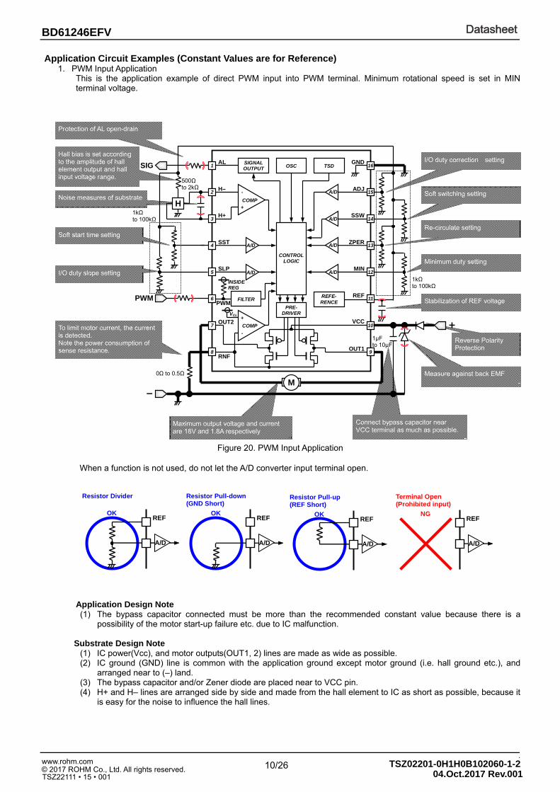
Application Circuit Examples (Constant Values are for Reference) 1. PWM Input Application
This is the application example of direct PWM input into PWM terminal. Minimum rotational speed is set in MIN terminal voltage.
When a function is not used, do not let the A/D converter input terminal open.
Application Design Note (1) The bypass capacitor connected must be more than the recommended constant value because there is a
possibility of the motor start-up failure etc. due to IC malfunction.
Substrate Design Note (1) IC power(Vcc), and motor outputs(OUT1, 2) lines are made as wide as possible. (2) IC ground (GND) line is common with the application ground except motor ground (i.e. hall ground etc.), and
arranged near to (–) land. (3) The bypass capacitor and/or Zener diode are placed near to VCC pin. (4) H+ and H– lines are arranged side by side and made from the hall element to IC as short as possible, because it
is easy for the noise to influence the hall lines.
Figure 20. PWM Input Application
Reverse Polarity Protection
Measure against back EMF
Maximum output voltage and current are 18V and 1.8A respectively
Connect bypass capacitor near VCC terminal as much as possible.
Soft switching setting
Minimum duty setting
Stabilization of REF voltage
Re-circulate setting
Hall bias is set according to the amplitude of hall element output and hall input voltage range.
Protection of AL open-drain
To limit motor current, the current is detected. Note the power consumption of sense resistance.
Noise measures of substrate
I/O duty slope setting
+
PWM
-
M
H
SIG
500Ω to 2kΩ
0Ω to 0.5Ω
1μF to 10μF
1kΩ to 100kΩ
SST
OUT2
H+
H–
OUT1
VCC
MIN
ZPER
ADJ
TSD
CONTROL LOGIC
OSC
FILTER REF REFE-
RENCE
RNF
PRE- DRIVER
SSW
PWM
INSIDE REG
15
14
13
12
2
3
4
5
6
7
8
11
10
9
AL SIGNAL OUTPUT
1 GND
16
+
-
COMP
COMP
+
-
VCL
SLP
A/D
A/D A/D
A/D
A/D
A/D
1kΩ to 100kΩ
REF
Resistor Divider
OK
A/D
REF
Resistor Pull-down (GND Short)
OK
A/D
REF
Resistor Pull-up (REF Short)
OK
A/D
REF
A/D
NG
Terminal Open (Prohibited input)
Soft start time setting
I/O duty correction setting
DatasheetDatasheet
.
11/26 © 2017 ROHM Co., Ltd. All rights reserved. TSZ22111 • 15 • 001
www.rohm.com
BD61246EFV
TSZ02201-0H1H0B102060-1-2 04.Oct.2017 Rev.001
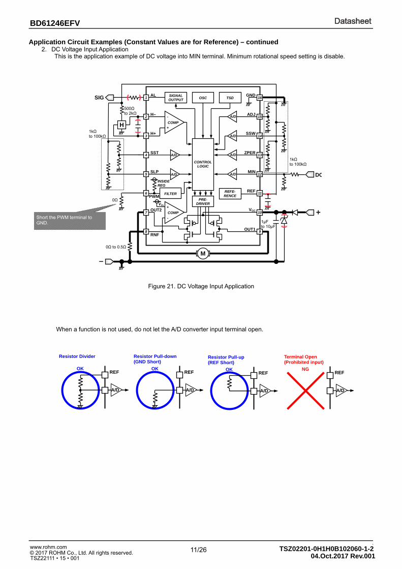
Application Circuit Examples (Constant Values are for Reference) – continued 2. DC Voltage Input Application
This is the application example of DC voltage into MIN terminal. Minimum rotational speed setting is disable.
When a function is not used, do not let the A/D converter input terminal open.
Figure 21. DC Voltage Input Application
Short the PWM terminal to GND.
REF
Resistor Divider
OK
A/D
REF
Resistor Pull-down (GND Short)
OK
A/D
REF
Resistor Pull-up (REF Short)
OK
A/D
REF
A/D
NG
Terminal Open (Prohibited input)
1μF to 10μF
+
-
M
H
SIG
500Ω to 2kΩ
0Ω to 0.5Ω
1kΩ to 100kΩ
SST
OUT2
H+
H–
OUT1
VCC
MIN
ZPER
ADJ
TSD
CONTROL LOGIC
OSC
FILTER REF REFE-
RENCE
RNF
PRE- DRIVER
SSW
PWM
INSIDE REG
15
14
13
12
2
3
4
5
6
7
8
11
10
9
AL SIGNAL OUTPUT
1 GND
16
+
-
COMP
COMP
+
-
VCL
SLP
A/D
A/D A/D
A/D
A/D
A/D
1kΩ to 100kΩ
DC
0Ω
DatasheetDatasheet
.
12/26 © 2017 ROHM Co., Ltd. All rights reserved. TSZ22111 • 15 • 001
www.rohm.com
BD61246EFV
TSZ02201-0H1H0B102060-1-2 04.Oct.2017 Rev.001
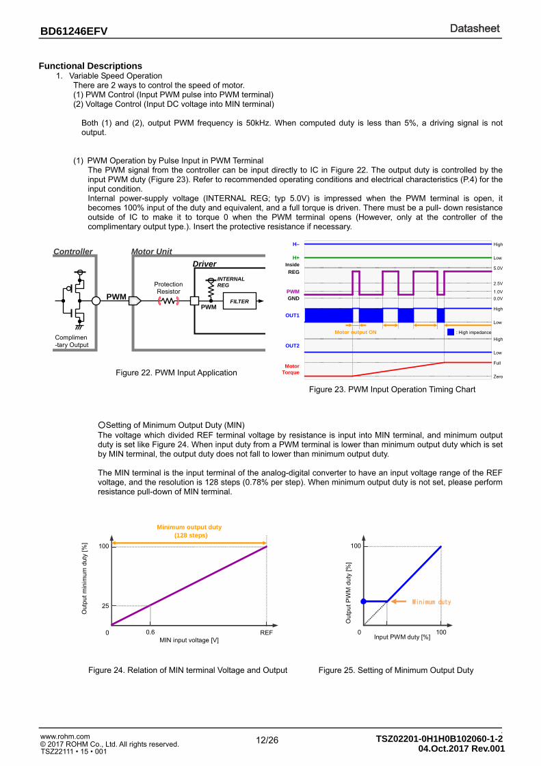
Functional Descriptions
1. Variable Speed Operation There are 2 ways to control the speed of motor. (1) PWM Control (Input PWM pulse into PWM terminal) (2) Voltage Control (Input DC voltage into MIN terminal) Both (1) and (2), output PWM frequency is 50kHz. When computed duty is less than 5%, a driving signal is not output.
(1) PWM Operation by Pulse Input in PWM Terminal
The PWM signal from the controller can be input directly to IC in Figure 22. The output duty is controlled by the input PWM duty (Figure 23). Refer to recommended operating conditions and electrical characteristics (P.4) for the input condition. Internal power-supply voltage (INTERNAL REG; typ 5.0V) is impressed when the PWM terminal is open, it becomes 100% input of the duty and equivalent, and a full torque is driven. There must be a pull- down resistance outside of IC to make it to torque 0 when the PWM terminal opens (However, only at the controller of the complimentary output type.). Insert the protective resistance if necessary.
Setting of Minimum Output Duty (MIN) The voltage which divided REF terminal voltage by resistance is input into MIN terminal, and minimum output duty is set like Figure 24. When input duty from a PWM terminal is lower than minimum output duty which is set by MIN terminal, the output duty does not fall to lower than minimum output duty. The MIN terminal is the input terminal of the analog-digital converter to have an input voltage range of the REF voltage, and the resolution is 128 steps (0.78% per step). When minimum output duty is not set, please perform resistance pull-down of MIN terminal.
Figure 22. PWM Input Application
PWM
Protection Resistor
Motor Unit
Driver
PWM FILTER
INTERNAL REG
Controller
Complimen -tary Output
Figure 23. PWM Input Operation Timing Chart
Inside
REG
OUT1
PWM
5.0V
1.0V
2.5V
OUT2
Low
High
Low
High
Low
High
H+
H–
0.0V GND
Zero
Full Motor
Torque
: High impedance Motor output ON
Figure 25. Setting of Minimum Output Duty Figure 24. Relation of MIN terminal Voltage and Output
Input PWM duty [%]
Out
pu
t PW
M d
uty
[%]
100
100
0
Minimum duty
0 REF
Minimum output duty (128 steps)
100
MIN input voltage [V]
Out
put
min
imu
m d
uty
[%]
0.6
25
DatasheetDatasheet
.
13/26 © 2017 ROHM Co., Ltd. All rights reserved. TSZ22111 • 15 • 001
www.rohm.com
BD61246EFV
TSZ02201-0H1H0B102060-1-2 04.Oct.2017 Rev.001
Functional Descriptions – continued
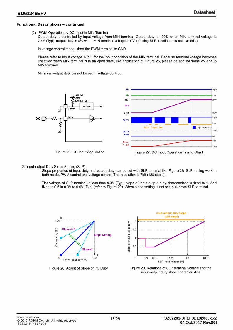
(2) PWM Operation by DC Input in MIN Terminal Output duty is controlled by input voltage from MIN terminal. Output duty is 100% when MIN terminal voltage is 2.4V (Typ), output duty is 0% when MIN terminal voltage is 0V. (If using SLP function, it is not like this.) In voltage control mode, short the PWM terminal to GND. Please refer to input voltage 1(P.3) for the input condition of the MIN terminal. Because terminal voltage becomes unsettled when MIN terminal is in an open state, like application of Figure 26, please be applied some voltage to MIN terminal. Minimum output duty cannot be set in voltage control.
2. Input-output Duty Slope Setting (SLP) Slope properties of input duty and output duty can be set with SLP terminal like Figure 28. SLP setting work in both mode, PWM control and voltage control. The resolution is 7bit (128 steps). The voltage of SLP terminal is less than 0.3V (Typ), slope of input-output duty characteristic is fixed to 1. And fixed to 0.5 in 0.3V to 0.6V (Typ) (refer to Figure 29). When slope setting is not set, pull-down SLP terminal.
REF
MIN
2.4V
0%
100%
Low
High
H+
H–
0.0V GND
Zero
Full Motor
Torque
OUT2 duty
OUT1 Low
: High Impedance Motor Output ON
High
Figure 26. DC Input Application Figure 27. DC Input Operation Timing Chart
Figure 28. Adjust of Slope of I/O Duty
PWM input duty [%] 100
100
0
Slope Setting
Slope=2
Slope=0.5
Out
pu
t du
ty [%
]
0.6 0 REF
0.5
Input-output duty slope (128 steps)
2
SLP input voltage [V]
Slo
pe o
f inp
ut-
outp
ut d
uty
1
1.5
1.2 1.8 0.3
Figure 29. Relations of SLP terminal voltage and the input-output duty slope characteristics
MIN
PWM FILTER
INSIDE REG
DC
200kΩ(Typ)
A/D
DatasheetDatasheet
.
14/26 © 2017 ROHM Co., Ltd. All rights reserved. TSZ22111 • 15 • 001
www.rohm.com
BD61246EFV
TSZ02201-0H1H0B102060-1-2 04.Oct.2017 Rev.001
Functional Descriptions – continued
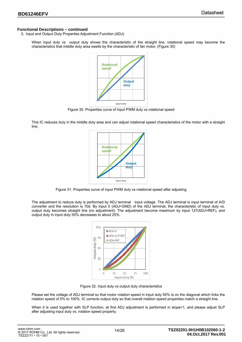
3. Input and Output Duty Properties Adjustment Function (ADJ)
When input duty vs output duty shows the characteristic of the straight line, rotational speed may become the characteristics that middle duty area swells by the characteristic of fan motor. (Figure 30)
Figure 30. Properties curve of input PWM duty vs rotational speed
This IC reduces duty in the middle duty area and can adjust rotational speed characteristics of the motor with a straight line.
Figure 31. Properties curve of input PWM duty vs rotational speed after adjusting
The adjustment to reduce duty is performed by ADJ terminal input voltage. The ADJ terminal is input terminal of A/D converter and the resolution is 7bit. By input 0 (ADJ=GND) of the ADJ terminal, the characteristic of input duty vs. output duty becomes straight line (no adjustment). The adjustment become maximum by input 127(ADJ=REF), and output duty in input duty 50% decreases to about 25%.
Figure 32. Input duty vs output duty characteristics
Please set the voltage of ADJ terminal so that motor rotation speed in input duty 50% is on the diagonal which links the rotation speed of 0% to 100%. IC corrects output duty so that overall rotation speed properties match a straight line.
When it is used together with SLP function, at first ADJ adjustment is performed in slope=1, and please adjust SLP after adjusting input duty vs. rotation speed property.
Output duty
Rotational speed
Output duty
Rotational speed
DatasheetDatasheet
.
15/26 © 2017 ROHM Co., Ltd. All rights reserved. TSZ22111 • 15 • 001
www.rohm.com
BD61246EFV
TSZ02201-0H1H0B102060-1-2 04.Oct.2017 Rev.001
Functional Descriptions – continued
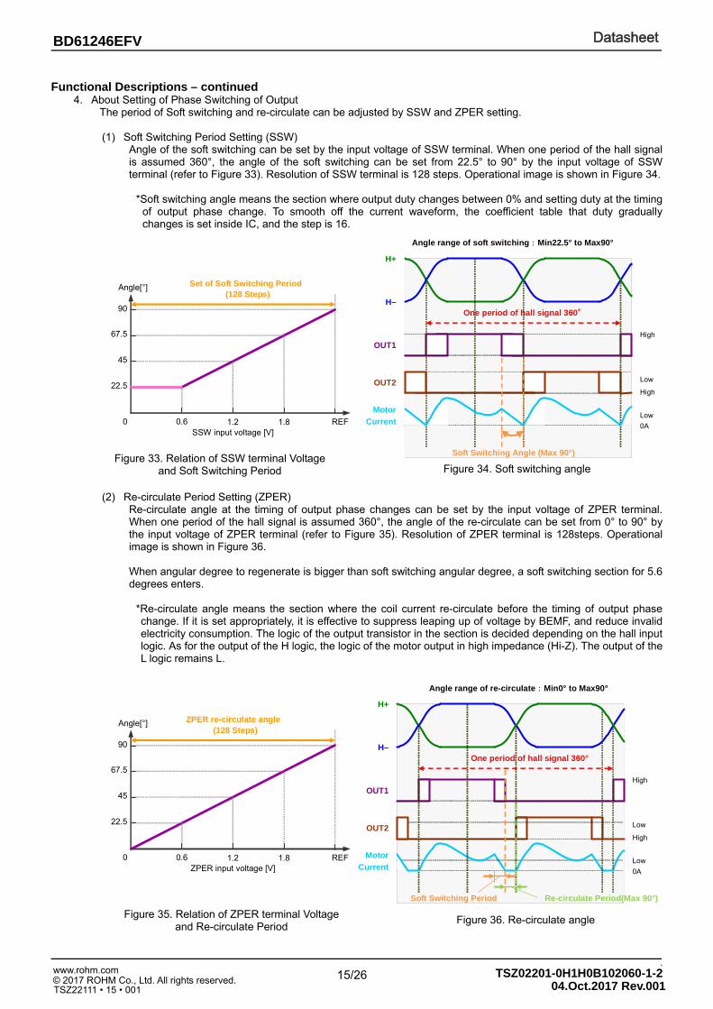
4. About Setting of Phase Switching of Output The period of Soft switching and re-circulate can be adjusted by SSW and ZPER setting.
(1) Soft Switching Period Setting (SSW)
Angle of the soft switching can be set by the input voltage of SSW terminal. When one period of the hall signal is assumed 360°, the angle of the soft switching can be set from 22.5° to 90° by the input voltage of SSW terminal (refer to Figure 33). Resolution of SSW terminal is 128 steps. Operational image is shown in Figure 34.
*Soft switching angle means the section where output duty changes between 0% and setting duty at the timing
of output phase change. To smooth off the current waveform, the coefficient table that duty gradually changes is set inside IC, and the step is 16.
(2) Re-circulate Period Setting (ZPER)
Re-circulate angle at the timing of output phase changes can be set by the input voltage of ZPER terminal. When one period of the hall signal is assumed 360°, the angle of the re-circulate can be set from 0° to 90° by the input voltage of ZPER terminal (refer to Figure 35). Resolution of ZPER terminal is 128steps. Operational image is shown in Figure 36. When angular degree to regenerate is bigger than soft switching angular degree, a soft switching section for 5.6 degrees enters.
*Re-circulate angle means the section where the coil current re-circulate before the timing of output phase change. If it is set appropriately, it is effective to suppress leaping up of voltage by BEMF, and reduce invalid electricity consumption. The logic of the output transistor in the section is decided depending on the hall input logic. As for the output of the H logic, the logic of the motor output in high impedance (Hi-Z). The output of the L logic remains L.
H+
H–
Low
High
Low
High
Motor
Current 0A
OUT1
OUT2
Angle range of soft switching:Min22.5° to Max90°
One period of hall signal 360°
Soft Switching Angle (Max 90°)
Figure 36. Re-circulate angle
Figure 34. Soft switching angle
0.6 0 REF
22.5
Set of Soft Switching Period (128 Steps)
90
SSW input voltage [V]
45
67.5
1.2 1.8
Angle[°]
Figure 33. Relation of SSW terminal Voltage and Soft Switching Period
0.6 0 REF
22.5
ZPER re-circulate angle (128 Steps)
90
ZPER input voltage [V]
45
67.5
1.2 1.8
Angle[°]
Figure 35. Relation of ZPER terminal Voltage and Re-circulate Period
H+
H–
Low
High
Low
High
Motor
Current 0A
OUT1
OUT2
Angle range of re-circulate:Min0° to Max90°
One period of hall signal 360°
Soft Switching Period Re-circulate Period(Max 90°)
DatasheetDatasheet
.
16/26 © 2017 ROHM Co., Ltd. All rights reserved. TSZ22111 • 15 • 001
www.rohm.com
BD61246EFV
TSZ02201-0H1H0B102060-1-2 04.Oct.2017 Rev.001
Functional Descriptions – continued
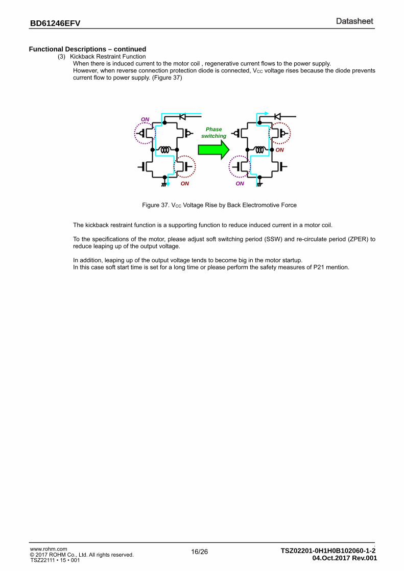
(3) Kickback Restraint Function When there is induced current to the motor coil , regenerative current flows to the power supply. However, when reverse connection protection diode is connected, VCC voltage rises because the diode prevents current flow to power supply. (Figure 37) The kickback restraint function is a supporting function to reduce induced current in a motor coil. To the specifications of the motor, please adjust soft switching period (SSW) and re-circulate period (ZPER) to reduce leaping up of the output voltage. In addition, leaping up of the output voltage tends to become big in the motor startup. In this case soft start time is set for a long time or please perform the safety measures of P21 mention.
Figure 37. VCC Voltage Rise by Back Electromotive Force
ON
Phase
switching
ON
ON
ON
DatasheetDatasheet
.
17/26 © 2017 ROHM Co., Ltd. All rights reserved. TSZ22111 • 15 • 001
www.rohm.com
BD61246EFV
TSZ02201-0H1H0B102060-1-2 04.Oct.2017 Rev.001
Functional Descriptions – continued
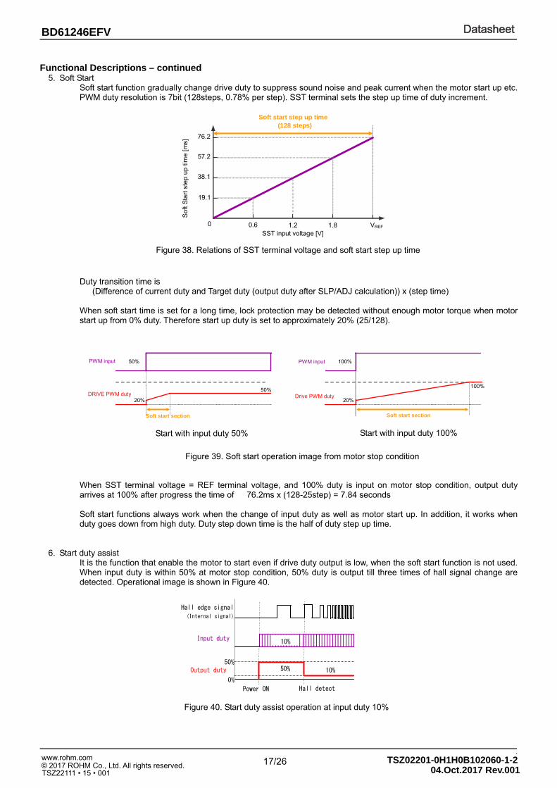
5. Soft Start Soft start function gradually change drive duty to suppress sound noise and peak current when the motor start up etc. PWM duty resolution is 7bit (128steps, 0.78% per step). SST terminal sets the step up time of duty increment. Duty transition time is (Difference of current duty and Target duty (output duty after SLP/ADJ calculation)) x (step time) When soft start time is set for a long time, lock protection may be detected without enough motor torque when motor start up from 0% duty. Therefore start up duty is set to approximately 20% (25/128).
When SST terminal voltage = REF terminal voltage, and 100% duty is input on motor stop condition, output duty arrives at 100% after progress the time of 76.2ms x (128-25step) = 7.84 seconds
Soft start functions always work when the change of input duty as well as motor start up. In addition, it works when duty goes down from high duty. Duty step down time is the half of duty step up time.
6. Start duty assist It is the function that enable the motor to start even if drive duty output is low, when the soft start function is not used. When input duty is within 50% at motor stop condition, 50% duty is output till three times of hall signal change are detected. Operational image is shown in Figure 40.
Start with input duty 50%
Sof
t Sta
rt s
tep
up ti
me
[m
s]
0.6 0 VREF
19.1
Soft start step up time (128 steps)
76.2
SST input voltage [V]
38.1
57.2
1.2 1.8
20%
PWM input
Drive PWM duty
Soft start section
100%
100%
PWM input
DRIVE PWM duty
Soft start section
50%
20%
50%
Figure 38. Relations of SST terminal voltage and soft start step up time
Start with input duty 100%
Figure 39. Soft start operation image from motor stop condition
Figure 40. Start duty assist operation at input duty 10%
Power ON
Input duty
50%
0%
10%
Hall detect
50% Output duty 10%
Hall edge signal
(Internal signal)
DatasheetDatasheet
.
18/26 © 2017 ROHM Co., Ltd. All rights reserved. TSZ22111 • 15 • 001
www.rohm.com
BD61246EFV
TSZ02201-0H1H0B102060-1-2 04.Oct.2017 Rev.001
Functional Descriptions – continued
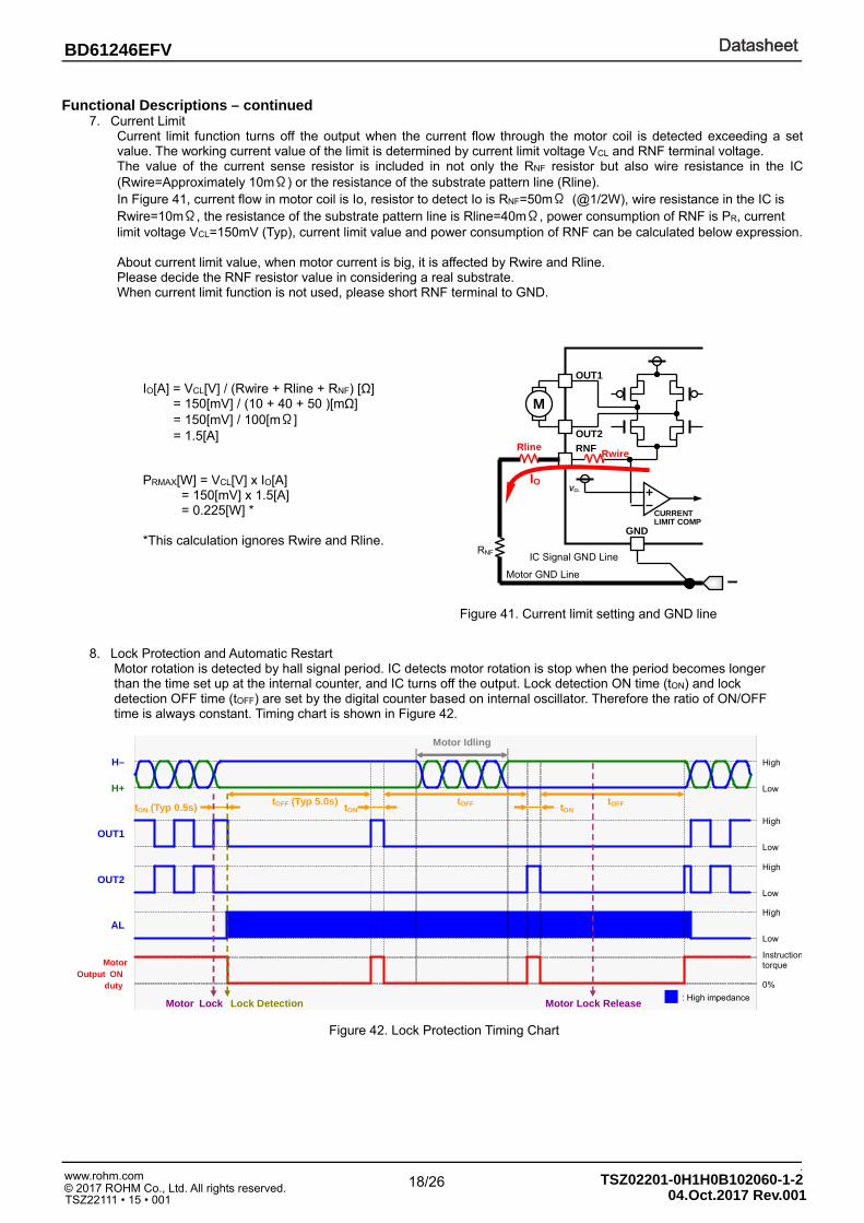
7. Current Limit Current limit function turns off the output when the current flow through the motor coil is detected exceeding a set value. The working current value of the limit is determined by current limit voltage VCL and RNF terminal voltage. The value of the current sense resistor is included in not only the RNF resistor but also wire resistance in the IC (Rwire=Approximately 10mΩ) or the resistance of the substrate pattern line (Rline). In Figure 41, current flow in motor coil is Io, resistor to detect Io is RNF=50mΩ (@1/2W), wire resistance in the IC is Rwire=10mΩ, the resistance of the substrate pattern line is Rline=40mΩ, power consumption of RNF is PR, current limit voltage VCL=150mV (Typ), current limit value and power consumption of RNF can be calculated below expression. About current limit value, when motor current is big, it is affected by Rwire and Rline. Please decide the RNF resistor value in considering a real substrate. When current limit function is not used, please short RNF terminal to GND.
8. Lock Protection and Automatic Restart
Motor rotation is detected by hall signal period. IC detects motor rotation is stop when the period becomes longer than the time set up at the internal counter, and IC turns off the output. Lock detection ON time (tON) and lock detection OFF time (tOFF) are set by the digital counter based on internal oscillator. Therefore the ratio of ON/OFF time is always constant. Timing chart is shown in Figure 42.
Figure 42. Lock Protection Timing Chart
Figure 41. Current limit setting and GND line
CURRENT LIMIT COMP
GND
Motor GND Line
RNF
-
IC Signal GND Line
VCL
OUT1
OUT2
RNF
IO
M
Rwire Rline
IO[A] = VCL[V] / (Rwire + Rline + RNF) [Ω] = 150[mV] / (10 + 40 + 50 )[mΩ] = 150[mV] / 100[mΩ] = 1.5[A]
PRMAX[W] = VCL[V] x IO[A] = 150[mV] x 1.5[A] = 0.225[W] *
*This calculation ignores Rwire and Rline.
tOFF (Typ 5.0s)
Low
High
: High impedance
OUT1 Low
High
Low
High
H+
H–
0%
Motor Output ON
duty
OUT2
AL Low
High
tON (Typ 0.5s) tON tOFF
Motor Lock Lock Detection Motor Lock Release
Motor Idling
tON tOFF
Instructiontorque
DatasheetDatasheet
.
19/26 © 2017 ROHM Co., Ltd. All rights reserved. TSZ22111 • 15 • 001
www.rohm.com
BD61246EFV
TSZ02201-0H1H0B102060-1-2 04.Oct.2017 Rev.001
2V
GND Hal
l inp
ut v
olta
ge r
ange
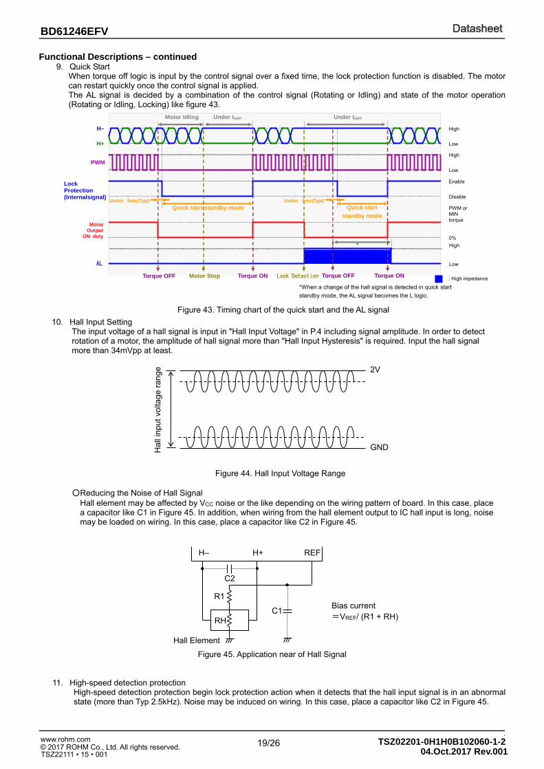
Functional Descriptions – continued 9. Quick Start
When torque off logic is input by the control signal over a fixed time, the lock protection function is disabled. The motor can restart quickly once the control signal is applied. The AL signal is decided by a combination of the control signal (Rotating or Idling) and state of the motor operation (Rotating or Idling, Locking) like figure 43.
10. Hall Input Setting
The input voltage of a hall signal is input in "Hall Input Voltage" in P.4 including signal amplitude. In order to detect rotation of a motor, the amplitude of hall signal more than "Hall Input Hysteresis" is required. Input the hall signal more than 34mVpp at least.
Figure 44. Hall Input Voltage Range Reducing the Noise of Hall Signal
Hall element may be affected by VCC noise or the like depending on the wiring pattern of board. In this case, place a capacitor like C1 in Figure 45. In addition, when wiring from the hall element output to IC hall input is long, noise may be loaded on wiring. In this case, place a capacitor like C2 in Figure 45.
Figure 45. Application near of Hall Signal
11. High-speed detection protection High-speed detection protection begin lock protection action when it detects that the hall input signal is in an abnormal state (more than Typ 2.5kHz). Noise may be induced on wiring. In this case, place a capacitor like C2 in Figure 45.
Figure 43. Timing chart of the quick start and the AL signal
C2
Hall Element
H– H+ REF
R1
RH C1
Bias current =VREF/ (R1 + RH)
Disable
Enable
PWM Low
High
Low
High
H+
H–
0%
Lock Protection (Internalsignal)
PWM or MIN torque
AL Low
High
Lock Detection
Under tOFF
: High impedance
*
*When a change of the hall signal is detected in quick start
standby mode, the AL signal becomes the L logic.
Motor Output
ON duty
Under 5ms(Typ)
Quick start standby mode
Motor Idling Under tOFF
Under 5ms(Typ)
Quick start
standby mode
Torque OFF Motor Stop Torque ON Torque OFF Torque ON

DatasheetDatasheet
.
20/26 © 2017 ROHM Co., Ltd. All rights reserved. TSZ22111 • 15 • 001
www.rohm.com
BD61246EFV
TSZ02201-0H1H0B102060-1-2 04.Oct.2017 Rev.001
I/O Equivalence Circuit (Resistance Values are Typical)
1. Power supply terminal 2. PWM input duty terminal 3. Hall input terminal
4. Variable speed control terminal 5. Reference voltage 6. Motor output terminal
Re-circulate angle setting terminal output terminal Output current detecting
Soft switching angle setting terminal resistor connecting terminal
7. Lock alarm signal
output terminal
SLP
SSW
MIN ZPER
VCC
GND
PWM
INSIDE REG
INSIDEREG
200kΩ
H+ H–
VCC
OUT1
OUT2
RNF
REF
VCC
AL
DatasheetDatasheet
.
21/26 © 2017 ROHM Co., Ltd. All rights reserved. TSZ22111 • 15 • 001
www.rohm.com
BD61246EFV
TSZ02201-0H1H0B102060-1-2 04.Oct.2017 Rev.001
Safety Measure
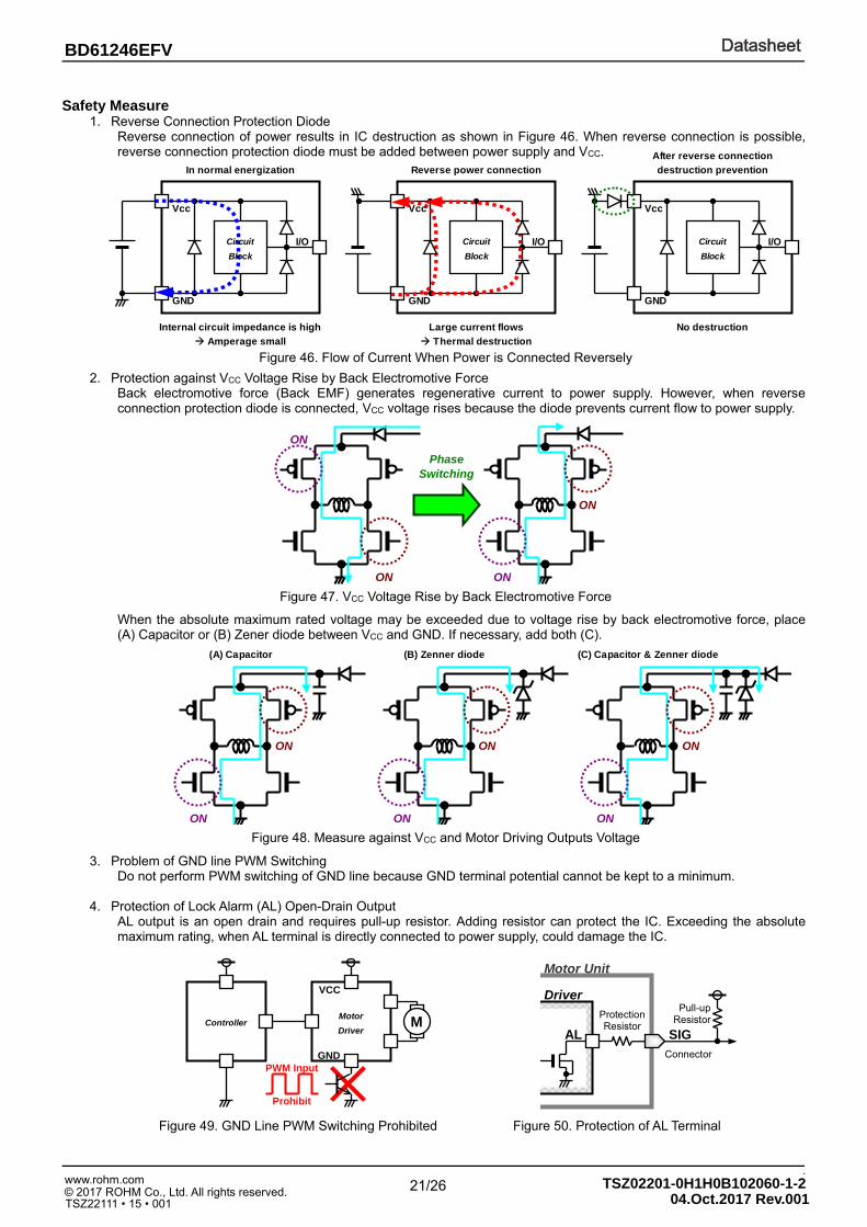
1. Reverse Connection Protection Diode Reverse connection of power results in IC destruction as shown in Figure 46. When reverse connection is possible, reverse connection protection diode must be added between power supply and VCC.
2. Protection against VCC Voltage Rise by Back Electromotive Force Back electromotive force (Back EMF) generates regenerative current to power supply. However, when reverse connection protection diode is connected, VCC voltage rises because the diode prevents current flow to power supply.
When the absolute maximum rated voltage may be exceeded due to voltage rise by back electromotive force, place (A) Capacitor or (B) Zener diode between VCC and GND. If necessary, add both (C).
3. Problem of GND line PWM Switching Do not perform PWM switching of GND line because GND terminal potential cannot be kept to a minimum.
4. Protection of Lock Alarm (AL) Open-Drain Output
AL output is an open drain and requires pull-up resistor. Adding resistor can protect the IC. Exceeding the absolute maximum rating, when AL terminal is directly connected to power supply, could damage the IC.
Figure 46. Flow of Current When Power is Connected Reversely
Figure 47. VCC Voltage Rise by Back Electromotive Force
Figure 48. Measure against VCC and Motor Driving Outputs Voltage
Figure 49. GND Line PWM Switching Prohibited Figure 50. Protection of AL Terminal
I/O
Vcc
GND
In normal energization
Internal circuit impedance is high
Amperage small
Circuit
Block
I/O
GND
Reverse power connection
Large current flows
Thermal destruction
Circuit
Block
Vcc
I/O
GND
After reverse connection
destruction prevention
No destruction
Circuit
Block
Vcc
ON
Phase Switching
ON
ON
ON
ON
ON
ON
ON
ON
ON
(A) Capacitor (B) Zenner diode (C) Capacitor & Zenner diode
VCC
GND
Prohibit
Motor
Driver Controller
PWM Input
M
AL
Driver
Protection Resistor
Motor Unit
Pull-upResistor
SIG
Connector
DatasheetDatasheet
.
22/26 © 2017 ROHM Co., Ltd. All rights reserved. TSZ22111 • 15 • 001
www.rohm.com
BD61246EFV
TSZ02201-0H1H0B102060-1-2 04.Oct.2017 Rev.001
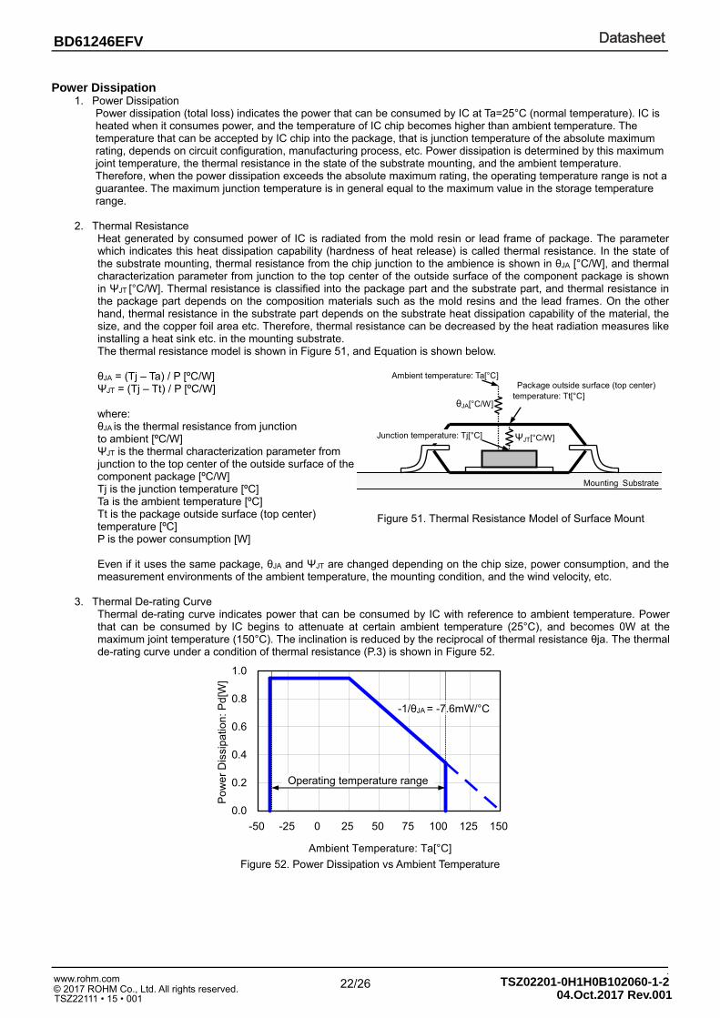
Power Dissipation 1. Power Dissipation
Power dissipation (total loss) indicates the power that can be consumed by IC at Ta=25°C (normal temperature). IC is heated when it consumes power, and the temperature of IC chip becomes higher than ambient temperature. The temperature that can be accepted by IC chip into the package, that is junction temperature of the absolute maximum rating, depends on circuit configuration, manufacturing process, etc. Power dissipation is determined by this maximum joint temperature, the thermal resistance in the state of the substrate mounting, and the ambient temperature. Therefore, when the power dissipation exceeds the absolute maximum rating, the operating temperature range is not a guarantee. The maximum junction temperature is in general equal to the maximum value in the storage temperature range.
2. Thermal Resistance
Heat generated by consumed power of IC is radiated from the mold resin or lead frame of package. The parameter which indicates this heat dissipation capability (hardness of heat release) is called thermal resistance. In the state of the substrate mounting, thermal resistance from the chip junction to the ambience is shown in θJA [°C/W], and thermal characterization parameter from junction to the top center of the outside surface of the component package is shown in ΨJT [°C/W]. Thermal resistance is classified into the package part and the substrate part, and thermal resistance in the package part depends on the composition materials such as the mold resins and the lead frames. On the other hand, thermal resistance in the substrate part depends on the substrate heat dissipation capability of the material, the size, and the copper foil area etc. Therefore, thermal resistance can be decreased by the heat radiation measures like installing a heat sink etc. in the mounting substrate. The thermal resistance model is shown in Figure 51, and Equation is shown below.
θJA = (Tj – Ta) / P [ºC/W] ΨJT = (Tj – Tt) / P [ºC/W]
where: θJA is the thermal resistance from junction to ambient [ºC/W] ΨJT is the thermal characterization parameter from junction to the top center of the outside surface of the component package [ºC/W] Tj is the junction temperature [ºC] Ta is the ambient temperature [ºC] Tt is the package outside surface (top center) temperature [ºC] P is the power consumption [W]
Even if it uses the same package, θJA and ΨJT are changed depending on the chip size, power consumption, and the measurement environments of the ambient temperature, the mounting condition, and the wind velocity, etc.
3. Thermal De-rating Curve
Thermal de-rating curve indicates power that can be consumed by IC with reference to ambient temperature. Power that can be consumed by IC begins to attenuate at certain ambient temperature (25°C), and becomes 0W at the maximum joint temperature (150°C). The inclination is reduced by the reciprocal of thermal resistance θja. The thermal de-rating curve under a condition of thermal resistance (P.3) is shown in Figure 52.
Figure 51. Thermal Resistance Model of Surface Mount
Figure 52. Power Dissipation vs Ambient Temperature
0.0
0.2
0.4
0.6
0.8
1.0
-50 -25 0 25 50 75 100 125 150
Ambient Temperature: Ta[°C]
Po
we
r D
issi
pa
tion:
Pd
[W]
Operating temperature range
-1/θJA = -7.6mW/°C
Junction temperature: Tj[°C]
Package outside surface (top center) temperature: Tt[°C]
Mounting Substrate
Ambient temperature: Ta[°C]
θJA[°C/W]
ΨJT[°C/W]
DatasheetDatasheet
.
23/26 © 2017 ROHM Co., Ltd. All rights reserved. TSZ22111 • 15 • 001
www.rohm.com
BD61246EFV
TSZ02201-0H1H0B102060-1-2 04.Oct.2017 Rev.001
Operational Notes
1. Reverse Connection of Power Supply Connecting the power supply in reverse polarity can damage the IC. Take precautions against reverse polarity when connecting the power supply, such as mounting an external diode between the power supply and the IC’s power supply pins.
2. Power Supply Lines Design the PCB layout pattern to provide low impedance supply lines. Furthermore, connect a capacitor to ground at all power supply pins. Consider the effect of temperature and aging on the capacitance value when using electrolytic capacitors.
3. Ground Voltage Ensure that no pins are at a voltage below that of the ground pin at any time, even during transient condition. However, pins that drive inductive loads (e.g. motor driver outputs, DC-DC converter outputs) may inevitably go below ground due to back EMF or electromotive force. In such cases, the user should make sure that such voltages going below ground will not cause the IC and the system to malfunction by examining carefully all relevant factors and conditions such as motor characteristics, supply voltage, operating frequency and PCB wiring to name a few.
4. Ground Wiring Pattern
When using both small-signal and large-current ground traces, the two ground traces should be routed separately but connected to a single ground at the reference point of the application board to avoid fluctuations in the small-signal ground caused by large currents. Also ensure that the ground traces of external components do not cause variations on the ground voltage. The ground lines must be as short and thick as possible to reduce line impedance.
5. Thermal Consideration
Should by any chance the power dissipation rating be exceeded the rise in temperature of the chip may result in deterioration of the properties of the chip. In case of exceeding this absolute maximum rating, increase the board size and copper area to prevent exceeding the Pd rating.
6. Recommended Operating Conditions
These conditions represent a range within which the expected characteristics of the IC can be approximately obtained. The electrical characteristics are guaranteed under the conditions of each parameter.
7. Inrush Current
When power is first supplied to the IC, it is possible that the internal logic may be unstable and inrush current may flow instantaneously due to the internal powering sequence and delays, especially if the IC has more than one power supply. Therefore, give special consideration to power coupling capacitance, power wiring, width of ground wiring, and routing of connections.
8. Operation Under Strong Electromagnetic Field
Operating the IC in the presence of a strong electromagnetic field may cause the IC to malfunction.
9. Testing on Application Boards When testing the IC on an application board, connecting a capacitor directly to a low-impedance output pin may subject the IC to stress. Always discharge capacitors completely after each process or step. The IC’s power supply should always be turned off completely before connecting or removing it from the test setup during the inspection process. To prevent damage from static discharge, ground the IC during assembly and use similar precautions during transport and storage.
DatasheetDatasheet
.
24/26 © 2017 ROHM Co., Ltd. All rights reserved. TSZ22111 • 15 • 001
www.rohm.com
BD61246EFV
TSZ02201-0H1H0B102060-1-2 04.Oct.2017 Rev.001
Operational Notes – continued
10. Inter-pin Short and Mounting Errors Ensure that the direction and position are correct when mounting the IC on the PCB. Incorrect mounting may result in damaging the IC. Avoid nearby pins being shorted to each other especially to ground, power supply and output pin. Inter-pin shorts could be due to many reasons such as metal particles, water droplets (in very humid environment) and unintentional solder bridge deposited in between pins during assembly to name a few.
11. Unused Input Pins
Input pins of an IC are often connected to the gate of a MOS transistor. The gate has extremely high impedance and extremely low capacitance. If left unconnected, the electric field from the outside can easily charge it. The small charge acquired in this way is enough to produce a significant effect on the conduction through the transistor and cause unexpected operation of the IC. So unless otherwise specified, unused input pins should be connected to the power supply or ground line.
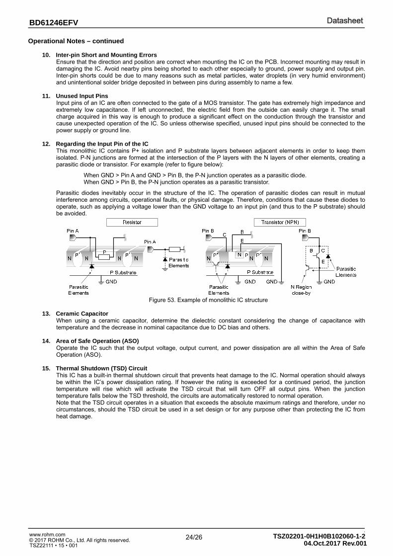
12. Regarding the Input Pin of the IC
This monolithic IC contains P+ isolation and P substrate layers between adjacent elements in order to keep them isolated. P-N junctions are formed at the intersection of the P layers with the N layers of other elements, creating a parasitic diode or transistor. For example (refer to figure below):
When GND > Pin A and GND > Pin B, the P-N junction operates as a parasitic diode. When GND > Pin B, the P-N junction operates as a parasitic transistor.
Parasitic diodes inevitably occur in the structure of the IC. The operation of parasitic diodes can result in mutual interference among circuits, operational faults, or physical damage. Therefore, conditions that cause these diodes to operate, such as applying a voltage lower than the GND voltage to an input pin (and thus to the P substrate) should be avoided.
Figure 53. Example of monolithic IC structure
13. Ceramic Capacitor When using a ceramic capacitor, determine the dielectric constant considering the change of capacitance with temperature and the decrease in nominal capacitance due to DC bias and others.
14. Area of Safe Operation (ASO) Operate the IC such that the output voltage, output current, and power dissipation are all within the Area of Safe Operation (ASO).
15. Thermal Shutdown (TSD) Circuit This IC has a built-in thermal shutdown circuit that prevents heat damage to the IC. Normal operation should always be within the IC’s power dissipation rating. If however the rating is exceeded for a continued period, the junction temperature will rise which will activate the TSD circuit that will turn OFF all output pins. When the junction temperature falls below the TSD threshold, the circuits are automatically restored to normal operation. Note that the TSD circuit operates in a situation that exceeds the absolute maximum ratings and therefore, under no circumstances, should the TSD circuit be used in a set design or for any purpose other than protecting the IC from heat damage.
DatasheetDatasheet
.
25/26 © 2017 ROHM Co., Ltd. All rights reserved. TSZ22111 • 15 • 001
www.rohm.com
BD61246EFV
TSZ02201-0H1H0B102060-1-2 04.Oct.2017 Rev.001
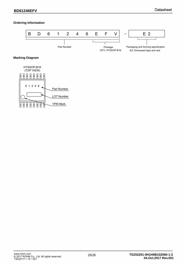
Ordering Information
Marking Diagram
B D 6 1 4 6 F E
Part Number Package ・EFV; HTSSOP-B16
V
Packaging and forming specification
- 2 2
・E2: Embossed tape and reel
E
6 1 2 4 6
HTSSOP-B16 (TOP VIEW)
Part Number
LOT Number
1PIN Mark
DatasheetDatasheet
.
26/26 © 2017 ROHM Co., Ltd. All rights reserved. TSZ22111 • 15 • 001
www.rohm.com
BD61246EFV
TSZ02201-0H1H0B102060-1-2 04.Oct.2017 Rev.001
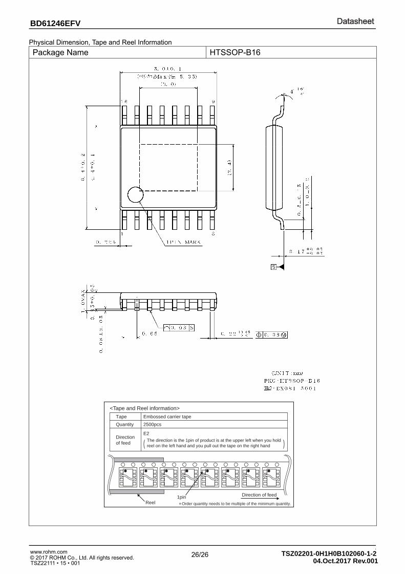
Physical Dimension, Tape and Reel Information
Package Name HTSSOP-B16
∗ Order quantity needs to be multiple of the minimum quantity.
<Tape and Reel information>
Embossed carrier tapeTape
Quantity
Direction of feed
The direction is the 1pin of product is at the upper left when you hold reel on the left hand and you pull out the tape on the right hand
2500pcs
E2
( )
Direction of feed
Reel1pin

Notice-PGA-E Rev.003
© 2015 ROHM Co., Ltd. All rights reserved.
Notice
Precaution on using ROHM Products 1. Our Products are designed and manufactured for application in ordinary electronic equipments (such as AV equipment,
OA equipment, telecommunication equipment, home electronic appliances, amusement equipment, etc.). If you intend to use our Products in devices requiring extremely high reliability (such as medical equipment
(Note 1), transport
equipment, traffic equipment, aircraft/spacecraft, nuclear power controllers, fuel controllers, car equipment including car accessories, safety devices, etc.) and whose malfunction or failure may cause loss of human life, bodily injury or serious damage to property (“Specific Applications”), please consult with the ROHM sales representative in advance. Unless otherwise agreed in writing by ROHM in advance, ROHM shall not be in any way responsible or liable for any damages, expenses or losses incurred by you or third parties arising from the use of any ROHM’s Products for Specific Applications.
(Note1) Medical Equipment Classification of the Specific Applications
JAPAN USA EU CHINA
CLASSⅢ CLASSⅢ
CLASSⅡb CLASSⅢ
CLASSⅣ CLASSⅢ
2. ROHM designs and manufactures its Products subject to strict quality control system. However, semiconductor
products can fail or malfunction at a certain rate. Please be sure to implement, at your own responsibilities, adequate safety measures including but not limited to fail-safe design against the physical injury, damage to any property, which a failure or malfunction of our Products may cause. The following are examples of safety measures:
[a] Installation of protection circuits or other protective devices to improve system safety [b] Installation of redundant circuits to reduce the impact of single or multiple circuit failure
3. Our Products are designed and manufactured for use under standard conditions and not under any special or extraordinary environments or conditions, as exemplified below. Accordingly, ROHM shall not be in any way responsible or liable for any damages, expenses or losses arising from the use of any ROHM’s Products under any special or extraordinary environments or conditions. If you intend to use our Products under any special or extraordinary environments or conditions (as exemplified below), your independent verification and confirmation of product performance, reliability, etc, prior to use, must be necessary:
[a] Use of our Products in any types of liquid, including water, oils, chemicals, and organic solvents [b] Use of our Products outdoors or in places where the Products are exposed to direct sunlight or dust [c] Use of our Products in places where the Products are exposed to sea wind or corrosive gases, including Cl2,
H2S, NH3, SO2, and NO2
[d] Use of our Products in places where the Products are exposed to static electricity or electromagnetic waves [e] Use of our Products in proximity to heat-producing components, plastic cords, or other flammable items [f] Sealing or coating our Products with resin or other coating materials [g] Use of our Products without cleaning residue of flux (even if you use no-clean type fluxes, cleaning residue of
flux is recommended); or Washing our Products by using water or water-soluble cleaning agents for cleaning residue after soldering
[h] Use of the Products in places subject to dew condensation
4. The Products are not subject to radiation-proof design. 5. Please verify and confirm characteristics of the final or mounted products in using the Products. 6. In particular, if a transient load (a large amount of load applied in a short period of time, such as pulse. is applied,
confirmation of performance characteristics after on-board mounting is strongly recommended. Avoid applying power exceeding normal rated power; exceeding the power rating under steady-state loading condition may negatively affect product performance and reliability.
7. De-rate Power Dissipation depending on ambient temperature. When used in sealed area, confirm that it is the use in
the range that does not exceed the maximum junction temperature. 8. Confirm that operation temperature is within the specified range described in the product specification. 9. ROHM shall not be in any way responsible or liable for failure induced under deviant condition from what is defined in
this document.
Precaution for Mounting / Circuit board design 1. When a highly active halogenous (chlorine, bromine, etc.) flux is used, the residue of flux may negatively affect product
performance and reliability.
2. In principle, the reflow soldering method must be used on a surface-mount products, the flow soldering method must be used on a through hole mount products. If the flow soldering method is preferred on a surface-mount products, please consult with the ROHM representative in advance.
For details, please refer to ROHM Mounting specification

Notice-PGA-E Rev.003
© 2015 ROHM Co., Ltd. All rights reserved.
Precautions Regarding Application Examples and External Circuits 1. If change is made to the constant of an external circuit, please allow a sufficient margin considering variations of the
characteristics of the Products and external components, including transient characteristics, as well as static characteristics.
2. You agree that application notes, reference designs, and associated data and information contained in this document
are presented only as guidance for Products use. Therefore, in case you use such information, you are solely responsible for it and you must exercise your own independent verification and judgment in the use of such information contained in this document. ROHM shall not be in any way responsible or liable for any damages, expenses or losses incurred by you or third parties arising from the use of such information.
Precaution for Electrostatic This Product is electrostatic sensitive product, which may be damaged due to electrostatic discharge. Please take proper caution in your manufacturing process and storage so that voltage exceeding the Products maximum rating will not be applied to Products. Please take special care under dry condition (e.g. Grounding of human body / equipment / solder iron, isolation from charged objects, setting of Ionizer, friction prevention and temperature / humidity control).
Precaution for Storage / Transportation 1. Product performance and soldered connections may deteriorate if the Products are stored in the places where:
[a] the Products are exposed to sea winds or corrosive gases, including Cl2, H2S, NH3, SO2, and NO2 [b] the temperature or humidity exceeds those recommended by ROHM [c] the Products are exposed to direct sunshine or condensation [d] the Products are exposed to high Electrostatic
2. Even under ROHM recommended storage condition, solderability of products out of recommended storage time period may be degraded. It is strongly recommended to confirm solderability before using Products of which storage time is exceeding the recommended storage time period.
3. Store / transport cartons in the correct direction, which is indicated on a carton with a symbol. Otherwise bent leads
may occur due to excessive stress applied when dropping of a carton. 4. Use Products within the specified time after opening a humidity barrier bag. Baking is required before using Products of
which storage time is exceeding the recommended storage time period.
Precaution for Product Label A two-dimensional barcode printed on ROHM Products label is for ROHM’s internal use only.
Precaution for Disposition When disposing Products please dispose them properly using an authorized industry waste company.
Precaution for Foreign Exchange and Foreign Trade act Since concerned goods might be fallen under listed items of export control prescribed by Foreign exchange and Foreign trade act, please consult with ROHM in case of export.
Precaution Regarding Intellectual Property Rights 1. All information and data including but not limited to application example contained in this document is for reference
only. ROHM does not warrant that foregoing information or data will not infringe any intellectual property rights or any other rights of any third party regarding such information or data.
2. ROHM shall not have any obligations where the claims, actions or demands arising from the combination of the Products with other articles such as components, circuits, systems or external equipment (including software).
3. No license, expressly or implied, is granted hereby under any intellectual property rights or other rights of ROHM or any third parties with respect to the Products or the information contained in this document. Provided, however, that ROHM will not assert its intellectual property rights or other rights against you or your customers to the extent necessary to manufacture or sell products containing the Products, subject to the terms and conditions herein.
Other Precaution 1. This document may not be reprinted or reproduced, in whole or in part, without prior written consent of ROHM.
2. The Products may not be disassembled, converted, modified, reproduced or otherwise changed without prior written consent of ROHM.
3. In no event shall you use in any way whatsoever the Products and the related technical information contained in the Products or this document for any military purposes, including but not limited to, the development of mass-destruction weapons.
4. The proper names of companies or products described in this document are trademarks or registered trademarks of ROHM, its affiliated companies or third parties.

DatasheetDatasheet
Notice – WE Rev.001© 2015 ROHM Co., Ltd. All rights reserved.
General Precaution 1. Before you use our Pro ducts, you are requested to care fully read this document and fully understand its contents.
ROHM shall n ot be in an y way responsible or liabl e for fa ilure, malfunction or acci dent arising from the use of a ny ROHM’s Products against warning, caution or note contained in this document.
2. All information contained in this docume nt is current as of the issuing date and subj ect to change without any prior
notice. Before purchasing or using ROHM’s Products, please confirm the la test information with a ROHM sale s representative.
3. The information contained in this doc ument is provi ded on an “as is” basis and ROHM does not warrant that all
information contained in this document is accurate an d/or error-free. ROHM shall not be in an y way responsible or liable for any damages, expenses or losses incurred by you or third parties resulting from inaccuracy or errors of or concerning such information.
Datasheet
Part Number BD61246EFVPackage HTSSOP-B16Unit Quantity 2500Minimum Package Quantity 2500Packing Type TapingConstitution Materials List inquiryRoHS Yes
BD61246EFV - Web Page