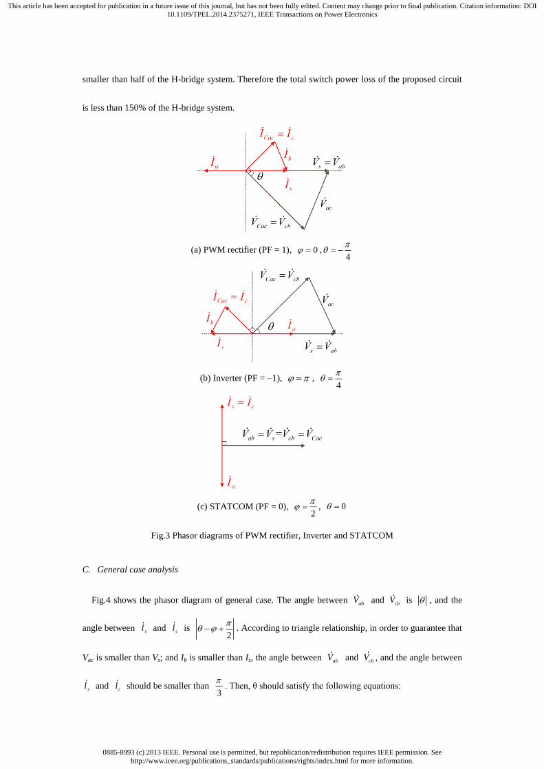
Embed Size (px)
Citation preview

0885-8993 (c) 2013 IEEE. Personal use is permitted, but republication/redistribution requires IEEE permission. Seehttp://www.ieee.org/publications_standards/publications/rights/index.html for more information.
This article has been accepted for publication in a future issue of this journal, but has not been fully edited. Content may change prior to final publication. Citation information: DOI10.1109/TPEL.2014.2375271, IEEE Transactions on Power Electronics
Abstract— Single-phase power conversion such as PWM rectifier, grid connected PV inverter
system, static synchronous compensator ( STATCOM ) all can be implemented by an H-bridge
inverter and a large electrolytic dc capacitor to absorb the ripple power pulsating at twice the
line frequency (2ω ripple power). This paper proposed a dc capacitor-less inverter for H-bridge
with minimum voltage and current stress. By adding another phase leg to control an ac capacitor,
the 2ω ripple power can be absorbed by the capacitor and theoretically 2ω ripples to the dc
capacitor can be eliminated completely. The H-bridge and the addition phase leg can be analyzed
together as an unbalanced three phase system. By adopting SVPWM control and choosing the
optimum ac capacitance and the voltage reference, the voltage and current stress of the switches
can be minimized to the same as the conventional H-bridge. The size of capacitor is reduced by
10 times compared to the conventional H-bridge system. Simulation and experimental results are
shown to prove the effectiveness of the proposed dc capacitor-less inverter and active power
decoupling method.
Corresponding Author: Runruo Chen is with the Department of Electrical and Computer
Engineering, Michigan State University, East Lansing, MI 48824 USA (e-mail: [email protected],
Phone: 5177754017).
DC capacitor-less inverter for single-phase power conversion
with minimum voltage and current stress
Runruo Chen, Student Member, IEEE, Yunting Liu, and Fang Zheng Peng, Fellow, IEEE

0885-8993 (c) 2013 IEEE. Personal use is permitted, but republication/redistribution requires IEEE permission. Seehttp://www.ieee.org/publications_standards/publications/rights/index.html for more information.
This article has been accepted for publication in a future issue of this journal, but has not been fully edited. Content may change prior to final publication. Citation information: DOI10.1109/TPEL.2014.2375271, IEEE Transactions on Power Electronics
Index Terms— dc capacitor-less inverter, single-phase power conversion, H-bridge, 2ω ripple,
power decoupling, SVPWM, current and voltage stress.
I. INTRODUCTION
-bridge has been widely used for single-phase power conversions, such as PWM rectifier, grid
connected PV inverter and static synchronous compensator (STATCOM) [1-5]. Although the power
factor (PF) for these applications could be different, however, they have a common inherent problem of
instantaneous power unbalance between dc power and ac power, which is time varying with a
double-frequency variation. In order to absorb the 2ω ripple power, conventional H-bridge needs a
bulky and expensive dc capacitor. The dc capacitance is given by
2 Vdc dc
SC
fV
where f is line frequency, S is the rated apparent power of the system, Vdc is the average voltage across
the dc capacitor, ΔVdc is the allowed peak-to-peak voltage ripple.
In order to reduce the dc capacitor bank, a great deal of research has been done on active power
decoupling methods [6-21]. The basic idea is using extra energy-storage components such as capacitor
or inductor, which permits much larger fluctuation of the voltage or current, to balance the 2ω ripple
power. Therefore, both the energy-storage component and the dc capacitor for switching ripple can be
minimized in size and weight. The key point is how to minimize the energy-storage component,
number of extra switches, and voltage/current stress of both switches and passive components.
In Fig. 1 (a), the energy-storage capacitor is connected to dc link and the capacitor voltage can only
be unipolar [9-11]. If the capacitor voltage reference is a full-wave rectified sine wave, the 2ω ripple
power can be fully transferred to the capacitor. However, the full-wave rectified sine reference, which
contains rich harmonic content, is difficult for the control system to track. Although it is possible to
H
0885-8993 (c) 2013 IEEE. Personal use is permitted, but republication/redistribution requires IEEE permission. Seehttp://www.ieee.org/publications_standards/publications/rights/index.html for more information.
This article has been accepted for publication in a future issue of this journal, but has not been fully edited. Content may change prior to final publication. Citation information: DOI10.1109/TPEL.2014.2375271, IEEE Transactions on Power Electronics
lower the harmonic content in the reference by increasing the energy-storage margin (therefore the
voltage does not go down to zero), this will compromise full utilization of the energy-storage capacitor.
(a)
(b)
(c)
Fig. 1 H-bridge with active power decoupling topologies
A single-phase PWM rectifier with the power decoupling ripple-port shown in Fig.1 (b) is proposed
in [12]. By adding any extra H-bridge to interface the energy-storage capacitor, the capacitor works in
ac mode and the voltage/current waveforms are sinusoidal. Since the energy-storage capacitor is fully
utilized, the capacitance is minimized. However, the system needs too many auxiliary switches, which

0885-8993 (c) 2013 IEEE. Personal use is permitted, but republication/redistribution requires IEEE permission. Seehttp://www.ieee.org/publications_standards/publications/rights/index.html for more information.
This article has been accepted for publication in a future issue of this journal, but has not been fully edited. Content may change prior to final publication. Citation information: DOI10.1109/TPEL.2014.2375271, IEEE Transactions on Power Electronics
increases the system complexity.
In [13-14], the PWM rectifier system shown in Fig.1 (c) consists of an H-bridge and an additional
phase leg connected to an AC capacitor, Cac. Compared to the topology in Fig.1 (b), the number of
extra switches is reduced. However, because of the adoption of SPWM control, the dc voltage is
greatly increased. As a result, the voltage stress of switches is higher; size and weight of passive
components are larger.
In this paper, the proposed dc capacitor-less inverter for single-phase power conversion has the same
topology in Fig.1(c). However the system is analyzed as an unbalance three-phase system. By adopting
SVPWM control and choosing the optimum ac capacitance and the voltage reference, the topologies
can be used for PWM rectifier (PF = 1), inverter (PF = 1) and STATCOM (PF = 0, current leading
voltage) without increasing both current and voltage stress. Since only two more switches are needed
and voltage/current stress is the same as the original H-bridge, the total device power rating is only
increased by 50%. The total size of capacitor (including the ac capacitor and the dc capacitor) of the
proposed system is reduced by 10 times compared to conventional H-bridge system.
II. THEORETICAL ANALYSIS
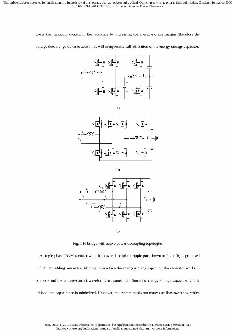
Taking the three output voltages of the three phase-legs as controlled voltage sources va, vb, vc, the
equivalent circuit for Fig.1 is shown in Fig. 2.
A. Power flow analysis
Suppose the grid voltage and the rated grid-side current to be:
sin( )
sin( )
s s
s s
v V t
i I t
,
and the voltage and current of the storage ac capacitor to be:
0885-8993 (c) 2013 IEEE. Personal use is permitted, but republication/redistribution requires IEEE permission. Seehttp://www.ieee.org/publications_standards/publications/rights/index.html for more information.
This article has been accepted for publication in a future issue of this journal, but has not been fully edited. Content may change prior to final publication. Citation information: DOI10.1109/TPEL.2014.2375271, IEEE Transactions on Power Electronics
sin( )
cos( ) cos( )
Cac Cac
Cac Cac ac Cac
v V t
i I t C V t
Fig. 2 Equivalent circuit of the system
Then, we can get the expression of grid power:
1[cos( ) cos(2 )]
2
1[cos( ) sin(2 )]
2 2
g s s s s
s s
p v i V I t
V I t
and the 2ω ripple power part of pg is
2
1sin(2 )
2 2s sp V I t
The instantaneous power generated by Cac can also be obtained:
21sin(2 2 )
2Cac Cac Cac ac Cacp v i C V t
To simplify the analysis, the power on filter inductors Lf1 and Lf2 (which are normally less than 5%
pu) is neglected. Then, the power of Cac should be controlled equal to the grid 2ω ripple power:
2Cacp p
Therefore, the magnitude and phase of vCac should satisfy the following equations:
2 =
1 1( ), or ( )+
2 2 2 2
ac Cac s sC V V I
If the decoupling capacitance is designed to be
sac
s
IC
V
the magnitude of the voltage and current of Cac will be:

0885-8993 (c) 2013 IEEE. Personal use is permitted, but republication/redistribution requires IEEE permission. Seehttp://www.ieee.org/publications_standards/publications/rights/index.html for more information.
This article has been accepted for publication in a future issue of this journal, but has not been fully edited. Content may change prior to final publication. Citation information: DOI10.1109/TPEL.2014.2375271, IEEE Transactions on Power Electronics
Cac s
Cac s
V V
I I
,
and the current and voltage stress of the system can be minimized.
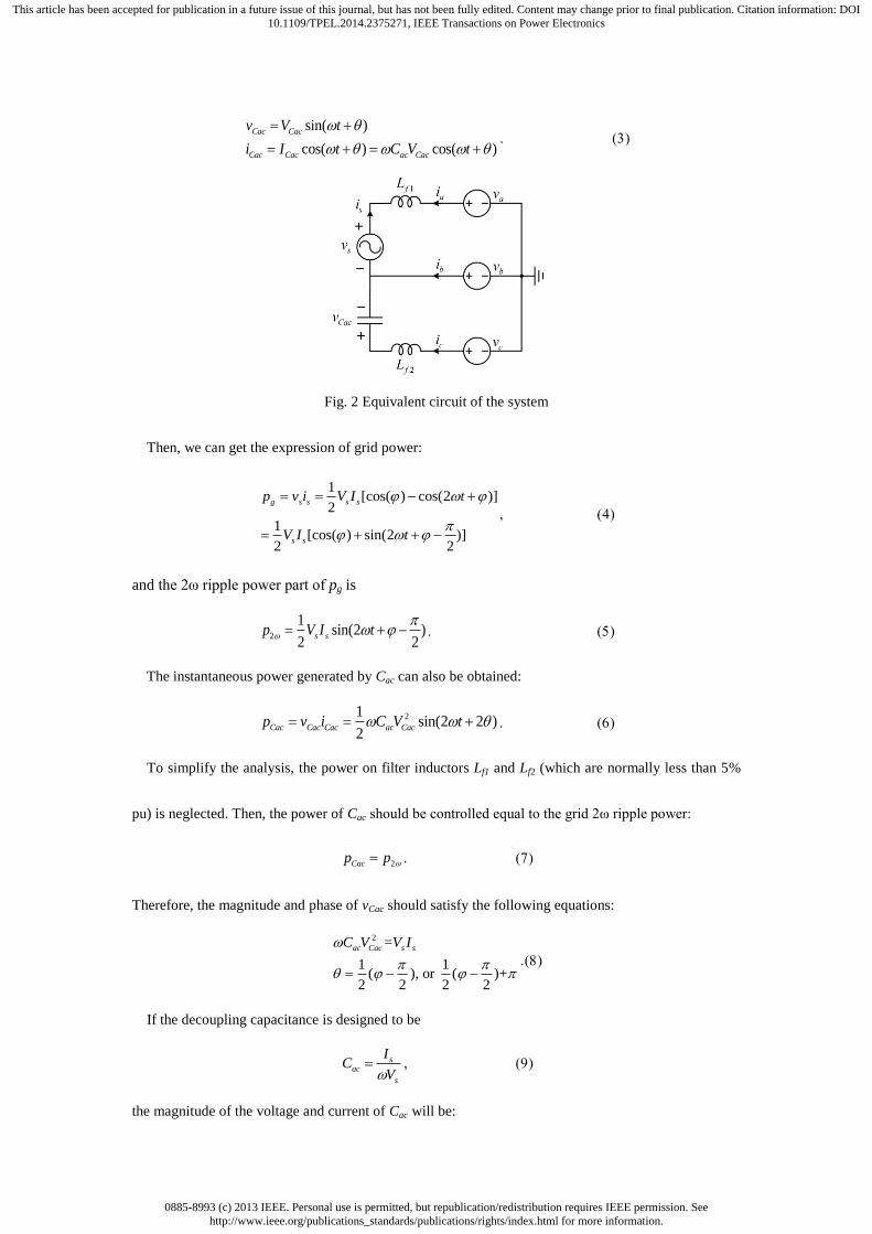
B. Specific cases analysis
According to the previous analysis, for any φ, there are two possible solutions of θ. Because the
system can be treated as an unbalanced three phase system, SVPWM can be adopted. For SVPWM, the
minimum dc voltage is determined by the maximum line-to-line voltage. For the rated power, we have:
ab cb s Cac
a c s Cac
V V V V
I I I I
,
For PWM rectifier, inverter and STATCOM, there will be two possible solutions for θ. Only by
choosing θ to be 4
,
4
and 0 for PWM rectifier, inverter and STATCOM respectively, the
magnitude of acV is smaller than Vs, and the magnitude of bI is smaller than Is. Then, the voltage
stress is 2 sV , and the current stress is 2 sI . Therefore, the voltage and current stress of switches are
equal to the original H-bridge system. If θ is not chosen properly, the current and voltage stress will be
greatly increased. For example, θ can also be π for STATCOM case. However, the magnitude of acV
will be 2Vs, and the magnitude of bI will be 2Is. and the voltage and current stress will be doubled.
Fig.3 shows the phasor diagrams of three specific cases with the minimum voltage and current stress.
Because the voltage and current stress of the proposed system and the H-bridge system are the same,
the two systems can use the same rating switches, and the power loss on switch can be directly
compared based on the phase current. For full rated power, phase A and phase C’s leg current of the
proposed circuit are same as the two leg of conventional H-bridge system, and phase B’s current of
proposed circuit are always smaller than H-bridge’s phase current. Then, the power loss on phase A
and C together are almost equal to the H-bridge system; and the power loss on phase B is always
0885-8993 (c) 2013 IEEE. Personal use is permitted, but republication/redistribution requires IEEE permission. Seehttp://www.ieee.org/publications_standards/publications/rights/index.html for more information.
This article has been accepted for publication in a future issue of this journal, but has not been fully edited. Content may change prior to final publication. Citation information: DOI10.1109/TPEL.2014.2375271, IEEE Transactions on Power Electronics
smaller than half of the H-bridge system. Therefore the total switch power loss of the proposed circuit
is less than 150% of the H-bridge system.
(a) PWM rectifier (PF = 1), 0 ,4
(b) Inverter (PF = 1), , 4
(c) STATCOM (PF = 0), 2
, 0
Fig.3 Phasor diagrams of PWM rectifier, Inverter and STATCOM
C. General case analysis
Fig.4 shows the phasor diagram of general case. The angle between abV and cbV is , and the
angle between sI and cI is 2
. According to triangle relationship, in order to guarantee that
Vac is smaller than Vs; and Ib is smaller than Is, the angle between abV and cbV , and the angle between
sI and cI should be smaller than 3
. Then, θ should satisfy the following equations:

0885-8993 (c) 2013 IEEE. Personal use is permitted, but republication/redistribution requires IEEE permission. Seehttp://www.ieee.org/publications_standards/publications/rights/index.html for more information.
This article has been accepted for publication in a future issue of this journal, but has not been fully edited. Content may change prior to final publication. Citation information: DOI10.1109/TPEL.2014.2375271, IEEE Transactions on Power Electronics
|
3
2 3|
.
Fig. 4 Phasor diagram of general case
To hold the inequality, the solution of θ is chosen as:
1
( )2 2
,
and accordingly φ should satisfy:
7
6 6
.
In other words, by choosing the optimum ac capacitance and suitable θ for Cac voltage reference, the
voltage and current stress can be equal to the original H-bridge system when 7
6 6
.
D. SVPWM control
The αβ transformation is defined as
1 1/ 2 1/ 22
3 0 3 / 2 3 / 2
1 1/ 22
3 0 3 / 2
a
b
c
s
Cac
vv
vv
v
v
v
.
Then we can get the trace of the space vector projected on αβ reference frame based on vs and vCac.
Because line-to-line voltage of the system is unbalanced, the space vector projection on αβ reference
frame is no longer a circle. Instead, the projection becomes be an ellipse or a line.
Fig.5 shows the space vector projections of PWM rectifier, inverter and STATCOM on αβ reference

0885-8993 (c) 2013 IEEE. Personal use is permitted, but republication/redistribution requires IEEE permission. Seehttp://www.ieee.org/publications_standards/publications/rights/index.html for more information.
This article has been accepted for publication in a future issue of this journal, but has not been fully edited. Content may change prior to final publication. Citation information: DOI10.1109/TPEL.2014.2375271, IEEE Transactions on Power Electronics
frame. The projections of PWM rectifier and inverter become an ellipse; the only difference is the
moving direction of the vector: PWM rectifier is clockwise, and inverter is counterclockwise. The
projection of STATCOM is a line, the vector moves back and forth along the line.
(a) PWM rectifier (PF = 1)
(b) Inverter (PF = 1)
(c) STATCOM (PF = 0)
Fig. 5 Space vector projections on αβ reference frame
E. Comparison between SVPWM and SPWM
In order to compare the minimum dc voltage requirement for SPWM and SVPWM control, take
PWM rectifier case as an example. For SVPWM, the minimum dc voltage is determined by the

0885-8993 (c) 2013 IEEE. Personal use is permitted, but republication/redistribution requires IEEE permission. Seehttp://www.ieee.org/publications_standards/publications/rights/index.html for more information.
This article has been accepted for publication in a future issue of this journal, but has not been fully edited. Content may change prior to final publication. Citation information: DOI10.1109/TPEL.2014.2375271, IEEE Transactions on Power Electronics
maximum peak value of line-to-line voltage. The maximum peak value of line-to-line voltage is
2 abV and 2 cbV which are all equal to 2 sV . Therefore, the minimum dc voltage is 2 sV .
For SPWM, va, vb, vc are sinusoid voltages. One possible solution is shown in Fig.6 [13] and
according to the triangle relationship, we have:
2 2 2
/ 2
/ 2
( / 2) cos45 0.737
a s
b s
c s s s s
V V
V V
V V V V V
.
The minimum dc voltage determined by the peak value of va, vb, vc. Since vc has the maximum peak
voltage, the minimum dc voltage is 2 2 CV , which is 47% larger than the dc voltage of SVPWM.
Fig. 6 Phase diagram of PWM rectifier for SPWM
III. CONTROL STRATEGY
A. Cac voltage and current reference
In the previous analysis, the filter inductors, Lf1 and Lf2 are neglected for simplification. In the
following analysis, in order to fully absorb the 2ω ripple power, the filer inductors are taken into
consideration to calculate the voltage and current reference of Cac.
Taking the reactive powers of Lf1 and Lf2 into account, the instantaneous power of dc capacitor from
the grid side becomes:

0885-8993 (c) 2013 IEEE. Personal use is permitted, but republication/redistribution requires IEEE permission. Seehttp://www.ieee.org/publications_standards/publications/rights/index.html for more information.
This article has been accepted for publication in a future issue of this journal, but has not been fully edited. Content may change prior to final publication. Citation information: DOI10.1109/TPEL.2014.2375271, IEEE Transactions on Power Electronics
1
2
1
1cos( )
2
1 1sin(2 ) sin(2 2 )
2 2 2
sab s s f s s s
s s f s
dip v i L i V I
dt
V I t L I t
,
and the 2ω ripple power component is:
_ 2
2
1 _ 2
1sin(2 )
2 2
1 1sin(2 2 ) sin(2 )
2 2
ab s s
f s ab ab
p V I t
L I t P t
.
where 2 2 2 3
_ 2 1 1( ) ( ) 2 sinab s s f s f s sP V I L I L V I , and
2
1
2
1
cos sin(2 )tan
sin cos(2 )
s s f s
ab
s s f s
V I L I
V I L I
.
Similarly, the instantaneous power of dc capacitor from Cac side becomes
2
2
2
1sin(2 2 )
12
Caccb Cac Cac f Cac
Cac
f
ac
dip v i L i
dt
Vt
LC
.
The power from Cac side should be controlled equal to the 2ω ripple power from the grid side:
_ 2cb abp p .
Therefore, the magnitude and phase of vCac should be:
_ 2 2
1( )
1
2
Cac ab f
ac
ab
V P LC
,
and the magnitude of iCac should be:
2
1Cac
Cac
f
ac
VI
LC
.
B. Control diagram
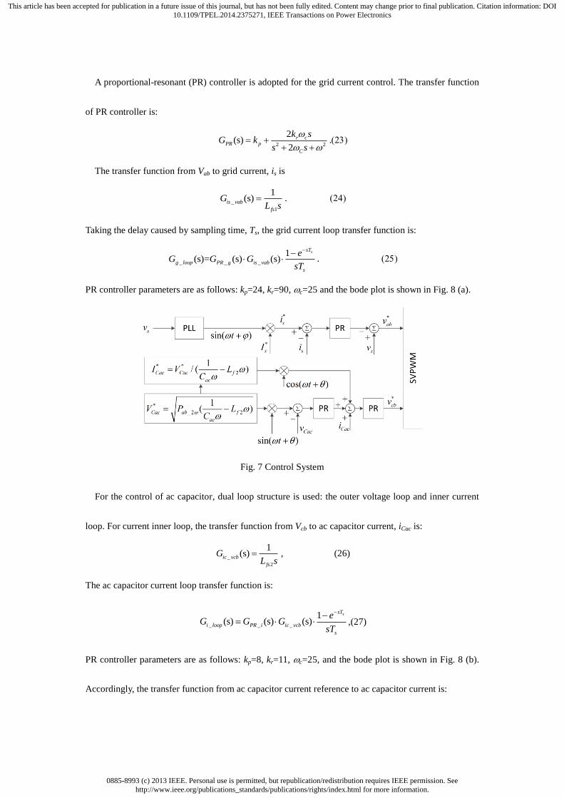
Fig. 7 shows the control system, which consists of two control loops. The first one is to control the
grid current and the second one is to control the voltage and current of the ac capacitor. The sampling
frequency is 20 kHz; Lfs1 and Lfs2 are 4.5% and 1.5% respectively.
0885-8993 (c) 2013 IEEE. Personal use is permitted, but republication/redistribution requires IEEE permission. Seehttp://www.ieee.org/publications_standards/publications/rights/index.html for more information.
This article has been accepted for publication in a future issue of this journal, but has not been fully edited. Content may change prior to final publication. Citation information: DOI10.1109/TPEL.2014.2375271, IEEE Transactions on Power Electronics
A proportional-resonant (PR) controller is adopted for the grid current control. The transfer function
of PR controller is:
2 2
2(s)
2
r cPR p
C
k sG k
s s
.
The transfer function from Vab to grid current, is is
_
1
1(s)is vab
fs
GL s
.
Taking the delay caused by sampling time, Ts, the grid current loop transfer function is:
_ _ _
1(s)= (s) (s)
ssT
g loop PR g is vab
s
eG G G
sT
.
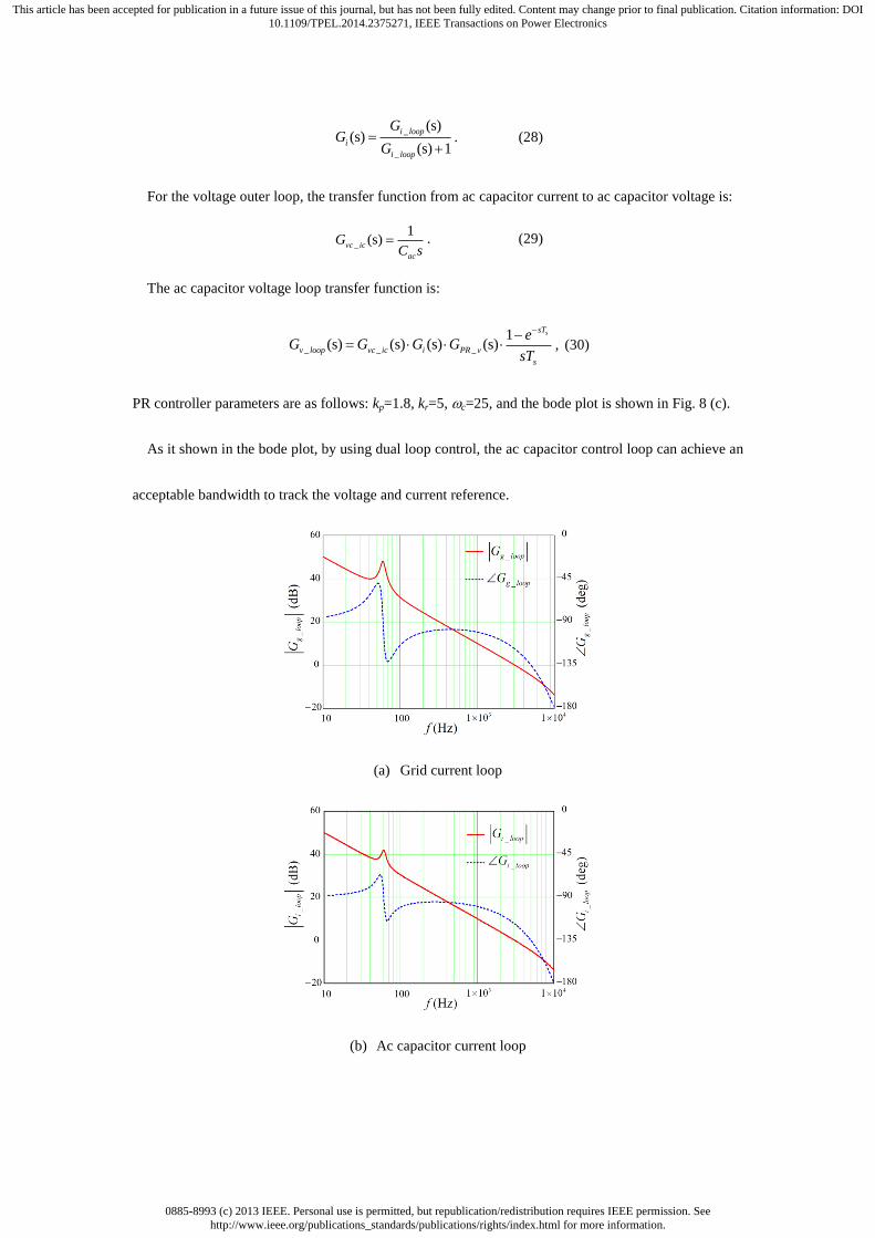
PR controller parameters are as follows: kp=24, kr=90, c=25 and the bode plot is shown in Fig. 8 (a).
Fig. 7 Control System
For the control of ac capacitor, dual loop structure is used: the outer voltage loop and inner current
loop. For current inner loop, the transfer function from Vcb to ac capacitor current, iCac is:
_
2
1(s)ic vcb
fs
GL s
, (26)
The ac capacitor current loop transfer function is:
_ _ _
1(s) (s) (s)
ssT
i loop PR i ic vcb
s
eG G G
sT
,(27)
PR controller parameters are as follows: kp=8, kr=11, c=25, and the bode plot is shown in Fig. 8 (b).
Accordingly, the transfer function from ac capacitor current reference to ac capacitor current is:
0885-8993 (c) 2013 IEEE. Personal use is permitted, but republication/redistribution requires IEEE permission. Seehttp://www.ieee.org/publications_standards/publications/rights/index.html for more information.
This article has been accepted for publication in a future issue of this journal, but has not been fully edited. Content may change prior to final publication. Citation information: DOI10.1109/TPEL.2014.2375271, IEEE Transactions on Power Electronics
_
_
(s)(s)
(s) 1
i loop
i
i loop
GG
G
. (28)
For the voltage outer loop, the transfer function from ac capacitor current to ac capacitor voltage is:
_
1(s)vc ic
ac
GC s
. (29)
The ac capacitor voltage loop transfer function is:
_ _ _
1(s) (s) (s) (s)
ssT
v loop vc ic i PR v
s
eG G G G
sT
, (30)
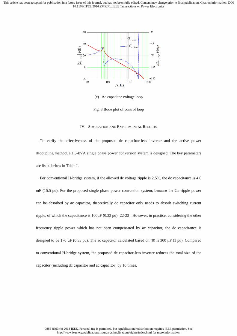
PR controller parameters are as follows: kp=1.8, kr=5, c=25, and the bode plot is shown in Fig. 8 (c).
As it shown in the bode plot, by using dual loop control, the ac capacitor control loop can achieve an
acceptable bandwidth to track the voltage and current reference.
(a) Grid current loop
(b) Ac capacitor current loop
0885-8993 (c) 2013 IEEE. Personal use is permitted, but republication/redistribution requires IEEE permission. Seehttp://www.ieee.org/publications_standards/publications/rights/index.html for more information.
This article has been accepted for publication in a future issue of this journal, but has not been fully edited. Content may change prior to final publication. Citation information: DOI10.1109/TPEL.2014.2375271, IEEE Transactions on Power Electronics
(c) Ac capacitor voltage loop
Fig. 8 Bode plot of control loop
IV. SIMULATION AND EXPERIMENTAL RESULTS
To verify the effectiveness of the proposed dc capacitor-lees inverter and the active power
decoupling method, a 1.5-kVA single phase power conversion system is designed. The key parameters
are listed below in Table I.
For conventional H-bridge system, if the allowed dc voltage ripple is 2.5%, the dc capacitance is 4.6
mF (15.5 pu). For the proposed single phase power conversion system, because the 2ω ripple power
can be absorbed by ac capacitor, theoretically dc capacitor only needs to absorb switching current
ripple, of which the capacitance is 100μF (0.33 pu) [22-23]. However, in practice, considering the other
frequency ripple power which has not been compensated by ac capacitor, the dc capacitance is
designed to be 170 μF (0.55 pu). The ac capacitor calculated based on (8) is 300 μF (1 pu). Compared
to conventional H-bridge system, the proposed dc capacitor-less inverter reduces the total size of the
capacitor (including dc capacitor and ac capacitor) by 10 times.
0885-8993 (c) 2013 IEEE. Personal use is permitted, but republication/redistribution requires IEEE permission. Seehttp://www.ieee.org/publications_standards/publications/rights/index.html for more information.
This article has been accepted for publication in a future issue of this journal, but has not been fully edited. Content may change prior to final publication. Citation information: DOI10.1109/TPEL.2014.2375271, IEEE Transactions on Power Electronics
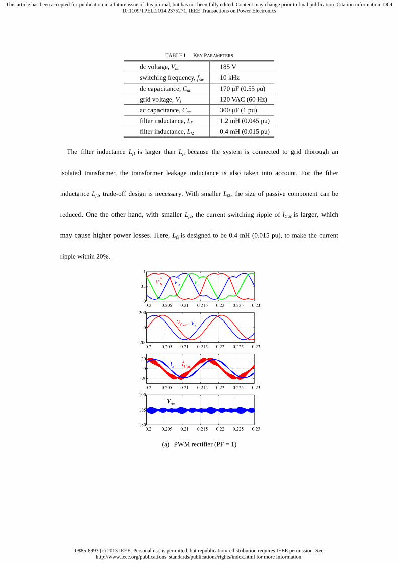
The filter inductance Lf1 is larger than Lf2 because the system is connected to grid thorough an
isolated transformer, the transformer leakage inductance is also taken into account. For the filter
inductance Lf2, trade-off design is necessary. With smaller Lf2, the size of passive component can be
reduced. One the other hand, with smaller Lf2, the current switching ripple of iCac is larger, which
may cause higher power losses. Here, Lf2 is designed to be 0.4 mH (0.015 pu), to make the current
ripple within 20%.
(a) PWM rectifier (PF = 1)
TABLE I KEY PARAMETERS
dc voltage, Vdc 185 V
switching frequency, fsw 10 kHz
dc capacitance, Cdc 170 μF (0.55 pu)
grid voltage, Vs 120 VAC (60 Hz)
ac capacitance, Cac 300 μF (1 pu)
filter inductance, Lf1 1.2 mH (0.045 pu)
filter inductance, Lf2 0.4 mH (0.015 pu)
0885-8993 (c) 2013 IEEE. Personal use is permitted, but republication/redistribution requires IEEE permission. Seehttp://www.ieee.org/publications_standards/publications/rights/index.html for more information.
This article has been accepted for publication in a future issue of this journal, but has not been fully edited. Content may change prior to final publication. Citation information: DOI10.1109/TPEL.2014.2375271, IEEE Transactions on Power Electronics
(b) inverter (PF = -1)
(c) STATCOM (PF = 0, current leading voltage)
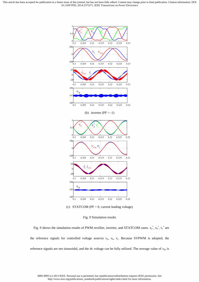
Fig. 9 Simulation results
Fig. 9 shows the simulation results of PWM rectifier, inverter, and STATCOM cases. va*, vb
*, vc
* are
the reference signals for controlled voltage sources va, vb, vc. Because SVPWM is adopted, the
reference signals are not sinusoidal, and the dc voltage can be fully utilized. The average value of vdc is
0885-8993 (c) 2013 IEEE. Personal use is permitted, but republication/redistribution requires IEEE permission. Seehttp://www.ieee.org/publications_standards/publications/rights/index.html for more information.
This article has been accepted for publication in a future issue of this journal, but has not been fully edited. Content may change prior to final publication. Citation information: DOI10.1109/TPEL.2014.2375271, IEEE Transactions on Power Electronics
185 V and the ripple voltage is within 3 V (1.5%). The relationship between vs, vCac, is, and iCac is
consistent with the theoretical analysis.
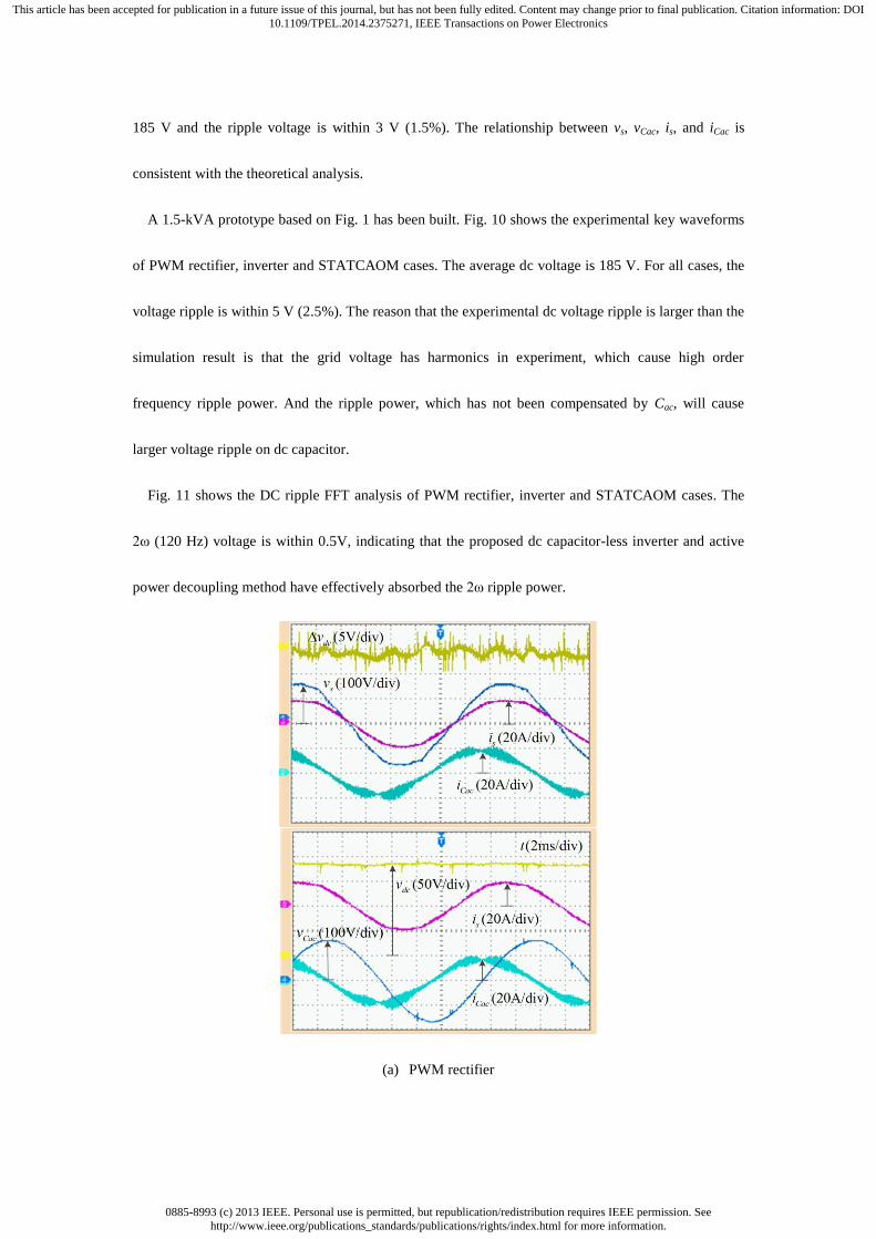
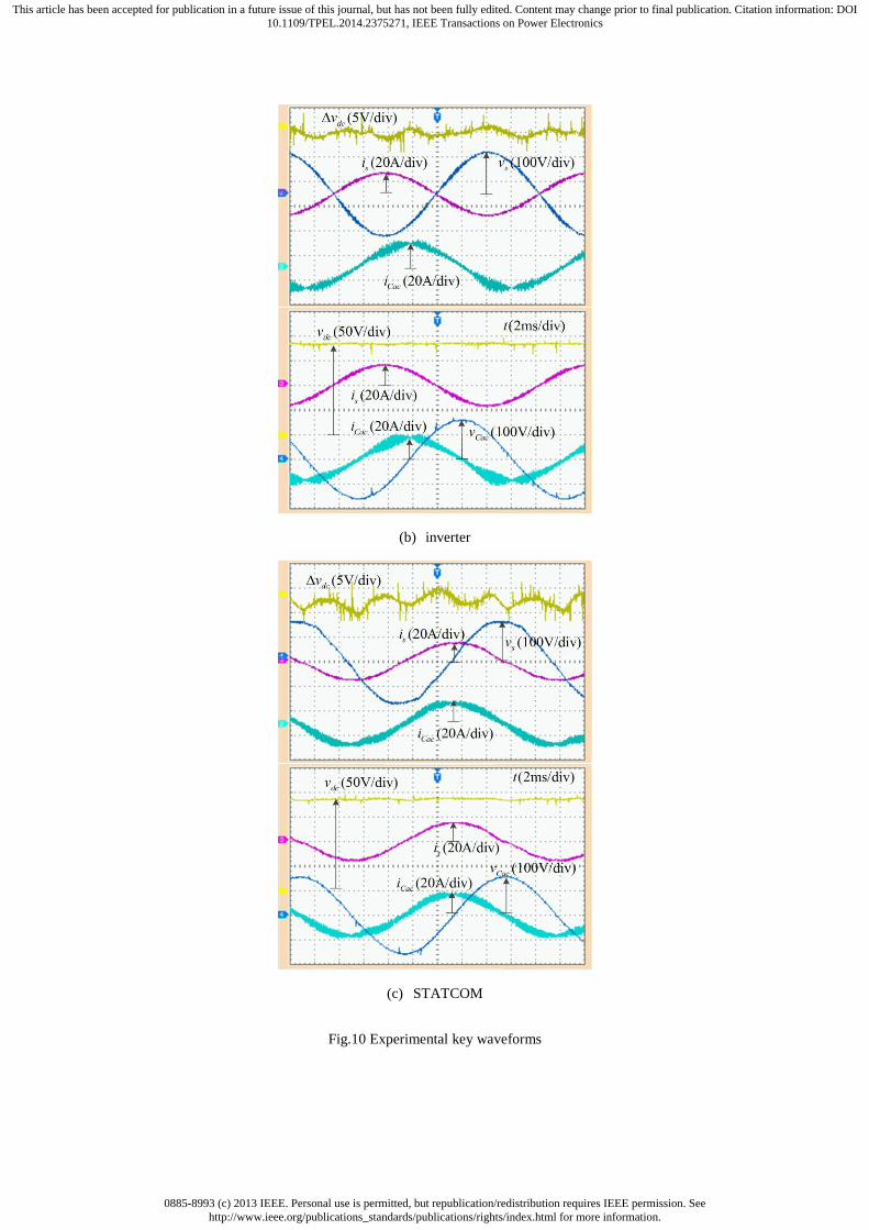
A 1.5-kVA prototype based on Fig. 1 has been built. Fig. 10 shows the experimental key waveforms
of PWM rectifier, inverter and STATCAOM cases. The average dc voltage is 185 V. For all cases, the
voltage ripple is within 5 V (2.5%). The reason that the experimental dc voltage ripple is larger than the
simulation result is that the grid voltage has harmonics in experiment, which cause high order
frequency ripple power. And the ripple power, which has not been compensated by Cac, will cause
larger voltage ripple on dc capacitor.
Fig. 11 shows the DC ripple FFT analysis of PWM rectifier, inverter and STATCAOM cases. The
2ω (120 Hz) voltage is within 0.5V, indicating that the proposed dc capacitor-less inverter and active
power decoupling method have effectively absorbed the 2ω ripple power.
(a) PWM rectifier
0885-8993 (c) 2013 IEEE. Personal use is permitted, but republication/redistribution requires IEEE permission. Seehttp://www.ieee.org/publications_standards/publications/rights/index.html for more information.
This article has been accepted for publication in a future issue of this journal, but has not been fully edited. Content may change prior to final publication. Citation information: DOI10.1109/TPEL.2014.2375271, IEEE Transactions on Power Electronics
(b) inverter
(c) STATCOM
Fig.10 Experimental key waveforms

0885-8993 (c) 2013 IEEE. Personal use is permitted, but republication/redistribution requires IEEE permission. Seehttp://www.ieee.org/publications_standards/publications/rights/index.html for more information.
This article has been accepted for publication in a future issue of this journal, but has not been fully edited. Content may change prior to final publication. Citation information: DOI10.1109/TPEL.2014.2375271, IEEE Transactions on Power Electronics
Fig.11 DC ripple FFT analysis
V. CONCLUSION
A DC capacitor-less inverter for single-phase power conversion with minimum voltage and current
stress is proposed. Only a AC capacitor to absorb 2 ripple power and a minimum DC capacitor to
absorb the switching ripple power are needed. By adopting SVPWM control and choosing the optimum
ac capacitance and the voltage reference, the voltage and current stress of the switches can be
minimized. The size of the capacitor is reduced by 10 times. Theoretical analysis and experimental
results have been presented. The simulation and experimental waveforms are consistent with the
theoretical analysis.
REFERENCES
[1] Dong Cao; Shuai Jiang; Peng, F.Z.; Yuan Li, "Low cost transformer isolated boost half-bridge micro-inverter for
single-phase grid-connected photovoltaic system," Applied Power Electronics Conference and Exposition (APEC), 2012
Twenty-Seventh Annual IEEE , vol., no., pp.71,78, 5-9 Feb. 2012
[2] Kjaer, S.B.; Pedersen, J.K.; Blaabjerg, F., "A review of single-phase grid-connected inverters for photovoltaic
modules," Industry Applications, IEEE Transactions on , vol.41, no.5, pp.1292,1306, Sept.-Oct. 2005
[3] Stihi, O.; Boon-Teck Ooi, "A single-phase controlled-current PWM rectifier," Power Electronics, IEEE Transactions on ,
vol.3, no.4, pp.453,459, Oct. 1988

0885-8993 (c) 2013 IEEE. Personal use is permitted, but republication/redistribution requires IEEE permission. Seehttp://www.ieee.org/publications_standards/publications/rights/index.html for more information.
This article has been accepted for publication in a future issue of this journal, but has not been fully edited. Content may change prior to final publication. Citation information: DOI10.1109/TPEL.2014.2375271, IEEE Transactions on Power Electronics
[4] Akagi, H.; Inoue, S.; Yoshii, T., "Control and Performance of a Transformerless Cascade PWM STATCOM With Star
Configuration," Industry Applications, IEEE Transactions on , vol.43, no.4, pp.1041,1049, July-aug. 2007
[5] Yiqiao Liang; Nwankpa, C.O., "A new type of STATCOM based on cascading voltage-source inverters with phase-shifted
unipolar SPWM," Industry Applications, IEEE Transactions on , vol.35, no.5, pp.1118,1123, Sep/Oct 1999
[6] Krein, P.T.; Balog, R.S.; Mirjafari, M., "Minimum Energy and Capacitance Requirements for Single-Phase Inverters and
Rectifiers Using a Ripple Port," Power Electronics, IEEE Transactions on , vol.27, no.11, pp.4690,4698, Nov. 2012
[7] Toshihisa Shimizu, Yasuhiro Jin, and Gunji Kimura, “DC ripple current reduction on a single-phase PWM voltage-source
rectifier,” IEEE Trans. Ind. Appl., vol. 36, no. 4, pp. 1419–1429, 2000
[8] Tsuno, K.; Shimizu, T.; Wada, K.; Ishii, K., "Optimization of the DC ripple energy compensating circuit on a single-phase
voltage source PWM rectifier," Power Electronics Specialists Conference, 2004. PESC 04. 2004 IEEE 35th Annual, vol.1,
pp.316,321 Vol.1, 20-25 June 2004
[9] Ruxi Wang; Wang, F.; Boroyevich, D.; Burgos, R.; Rixin Lai; Puqi Ning; Rajashekara, K., "A High Power Density
Single-Phase PWM Rectifier With Active Ripple Energy Storage," Power Electronics, IEEE Transactions on , vol.26, no.5,
pp.1430,1443, May 2011
[10] Ruxi Wang; Wang, F.; Rixin Lai; Puqi Ning; Burgos, R.; Boroyevich, D., "Study of Energy Storage Capacitor Reduction
for Single Phase PWM Rectifier," Applied Power Electronics Conference and Exposition, 2009. APEC 2009.
Twenty-Fourth Annual IEEE , pp.1177,1183, 15-19 Feb. 2009
[11] Kuo-Hen Chao; Po-Tai Cheng; Shimizu, T., "New control methods for single phase PWM regenerative rectifier with power
decoupling function," Power Electronics and Drive Systems, 2009. PEDS 2009. International Conference on , vol., no.,
pp.1091,1096, 2-5 Nov. 2009
[12] Harb, Souhib; Balog, Robert S., "Single-phase PWM rectifier with power decoupling ripple-port for double-line-frequency
ripple cancellation," Applied Power Electronics Conference and Exposition (APEC), 2013 Twenty-Eighth Annual IEEE,
March 2013
[13] Hongbo Li; Kai Zhang; Hui Zhao; Shengfang Fan; Jian Xiong, "Active Power Decoupling for High-Power Single-Phase
PWM Rectifiers," Power Electronics, IEEE Transactions on , vol.28, no.3, pp.1308,1319, March 2013
[14] Sisheng Liang; Xi Lu; Runruo Chen; Yang Liu; Shao Zhang; Peng, F.Z., "A solid state variable capacitor with minimum
DC capacitance," Applied Power Electronics Conference and Exposition (APEC), 2014 Twenty-Ninth Annual IEEE , vol.,
no., pp.3496,3501, 16-20 March 2014

0885-8993 (c) 2013 IEEE. Personal use is permitted, but republication/redistribution requires IEEE permission. Seehttp://www.ieee.org/publications_standards/publications/rights/index.html for more information.
This article has been accepted for publication in a future issue of this journal, but has not been fully edited. Content may change prior to final publication. Citation information: DOI10.1109/TPEL.2014.2375271, IEEE Transactions on Power Electronics
[15] Shengfang Fan; Yaosuo Xue; Kai Zhang, "A novel active power decoupling method for single-phase photovoltaic or
energy storage applications," Energy Conversion Congress and Exposition (ECCE), 2012 IEEE , vol., no., pp.2439,2446,
15-20 Sept. 2012
[16] Bush, C.R.; Bingsen Wang, "A single-phase current source solar inverter with reduced-size DC link," Energy Conversion
Congress and Exposition, 2009. ECCE 2009. IEEE , vol., no., pp.54,59, 20-24 Sept. 2009
[17] Quan Li; Wolfs, P., "A Review of the Single Phase Photovoltaic Module Integrated Converter Topologies With Three
Different DC Link Configurations," Power Electronics, IEEE Transactions on , vol.23, no.3, pp.1320,1333, May 2008
[18] Haibing Hu; Harb, S.; Kutkut, N.; Batarseh, I.; Shen, Z.J., "Power decoupling techniques for micro-inverters in PV
systems-a review," Energy Conversion Congress and Exposition (ECCE), 2010 IEEE , vol., no., pp.3235,3240, 12-16 Sept.
2010
[19] Kyritsis, A.C.; Papanikolaou, N.P.; Tatakis, E.C., "A novel Parallel Active Filter for Current Pulsation Smoothing on single
stage grid-connected AC-PV modules," Power Electronics and Applications, 2007 European Conference on , vol., no.,
pp.1,10, 2-5 Sept. 2007
[20] Xiong Liu; Peng Wang; Poh Chiang Loh; Blaabjerg, F.; Mingyu Xue, "Six switches solution for single-phase AC/DC/AC
converter with capability of second-order power mitigation in DC-link capacitor," Energy Conversion Congress and
Exposition (ECCE), 2011 IEEE , vol., no., pp.1368,1375, 17-22 Sept. 2011
[21] Blaabjerg, F.; Neacsu, D.O.; Pedersen, J.K., "Adaptive SVM to compensate DC-link voltage ripple for four-switch
three-phase voltage-source inverters," Power Electronics, IEEE Transactions on , vol.14, no.4, pp.743,752, Jul 1999
[22] Kieferndorf, F.D.; Forster, M.; Lipo, T.A, "Reduction of DC-bus capacitor ripple current with PAM/PWM
converter," Industry Applications, IEEE Transactions on , vol.40, no.2, pp.607,614, March-April 2004
[23] Xi Lu; Fang Zheng Peng, "Theoretical analysis of DC link capacitor current ripple reduction in the HEV DC-DC converter
and inverter system using a carrier modulation method," Energy Conversion Congress and Exposition (ECCE), 2012 IEEE ,
vol., no., pp.2833,2839, 15-20 Sept. 2012


![A Review On Various Multilevel Inverter Topologiesgjar.org/publishpaper/vol2issue1/d98r17.pdf · flying capacitor multilevel inverter and converter. Ryan et al [38] introduces a control](https://img.pdfslide.net/doc/110x75/5f0b58f67e708231d43011a6/a-review-on-various-multilevel-inverter-flying-capacitor-multilevel-inverter-and.jpg)