Embed Size (px)
Citation preview
1dc2026cfe
DEMO MANUAL DC2026C
DESCRIPTION
Linduino One Isolated Arduino-Compatible
Demonstration Board
Linear Technology’s DC2026 (called the Linduino® One) is compatible with the Arduino Uno microcontroller board. Arduino hardware consists of an Atmel microcontroller with a bootloader allowing quick in-circuit firmware up-dates. The software is a simple programming environment based on the AVRGCC compiler. This platform is popular because it is easy to use, both the hardware and software are open source, and it can be programmed in C. We find it an ideal way to demonstrate and distribute libraries for integrated circuits that have digital interfaces such as Inter-Integrated Circuit (I2C) and Serial Peripheral Interface (SPI). While the Linduino One is Arduino-compatible, it is not produced by the official Arduino team, and they do not receive any monetary support from this board. Please, consider supporting them by purchasing other items from: http://store.arduino.ccL, LT, LTC, LTM, Linear Technology, Linduino and the Linear logo are registered trademarks and QuikEval are trademarks of Linear Technology Corporation. All other trademarks are the property of their respective owners.
The Linduino One adds several features to the standard Arduino Uno board:
• A 14-pin QuikEval™ connector provides a direct connec-tion to a growing list of hundreds of Linear Technology demo boards, including ADCs, DACs, Power System Management, RF Synthesizers, System Monitor and Control, and many others.
• Selectable 5V, 3.3V, 2.5V, 1.8V logic levels and analog supply on QuikEval Connector
• An LTM®2884 provides galvanic isolation of USB data and power for both safety and noise rejection.
• Auxiliary 7V to 20V power input on isolated side, with conversion to 5V provided by an LT®3973 allowing high power operation up to 750mA.
Design files for this circuit board are available at http://www.linear.com/demo/DC2026C
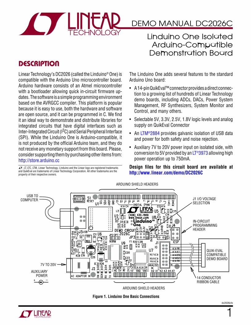
Figure 1. Linduino One Basic Connections
AUXILIARYPOWER
USB TOCOMPUTER
7V TO 20V
+ –
IN-CIRCUITPROGRAMMINGHEADER
J1 I/O VOLTAGESELECTION
ARDUINO SHIELD HEADERS
QUIK-EVALCOMPATIBLEDEMO BOARD
14 CONDUCTORRIBBON CABLE
ARDUINO SHIELD HEADERS
2dc2026cfe
DEMO MANUAL DC2026C
QUICK START GUIDEThe Linduino One comes preloaded with a DC590 emula-tor program (called a “sketch”) that allows attached demo boards to run with the standard QuikEval GUI software. This allows the functionality of the board to be verified before starting firmware development. After evaluation with QuikEval, the Linduino One can be reprogrammed with customer code. There is a top-level demonstration sketch for each part’s library that provides a text terminal interface to the board, demonstrating the library functions.
The Linduino One is also available as DC2026C-KIT, which includes a DC934 as an easy to use example daughter board. DC934 is the demonstration board for the LTC®2607 dual 16-bit, I2C digital to analog converter (DAC). This board also has an LTC2422 2-channel, 20-bit, SPI inter-face analog to digital converter (ADC) that reads back the DAC output. Thus, this board demonstrates operation of both SPI and I2C interfaces, and multichannel ADCs and DACs. The following sections describe the procedure for installing the required software and operating the DC934 with both QuikEval software and with a terminal based demo program.
While this manual describes operation with the DC934, the procedure applies to other boards as well.
Manual Software Installation
1) Download LTSketchbook.zip from www.linear.com/docs/43958. This is the entire code base for the Linduino board, including all demo code, libraries for individual devices, auxiliary functions, and HTML documentation. Extract this file to a location for working files, such as your “My Documents” directory or “C:\Projects”.
2) Note: If QuikEval is already installed, please update to the latest version by selecting Tools → Update Pro-gram, then proceed to step 3. If not, download and run QuikEval from www.linear.com/software. This installs the QuikEval program, as well as the FTDI USB drivers required for the Linduino One (and other Linear Tech-nology interface boards.) Drivers are also distributed with the Arduino IDE, but it is recommended to let QuikEval install the drivers to ensure compatibility with the Linduino One. You will be prompted to connect the board to the PC during installation. Once the installation is complete, quit QuikEval.
3) Download the Arduino Integrated Development Envi-ronment (IDE) from either http://arduino.cc/en/Main/Software or http://www.linear.com/designtools/linduino.php
(Version 1.6.4 is used in this manual.) This is not an installer; no installation is necessary. Extract the contents of this file to a convenient location for programs, such as “C:\Program Files”. The “Arduino.exe” file is the actual program file; double-click to open the Arduino IDE.
3dc2026cfe
DEMO MANUAL DC2026C
QUICK START GUIDEArduino IDE Setup
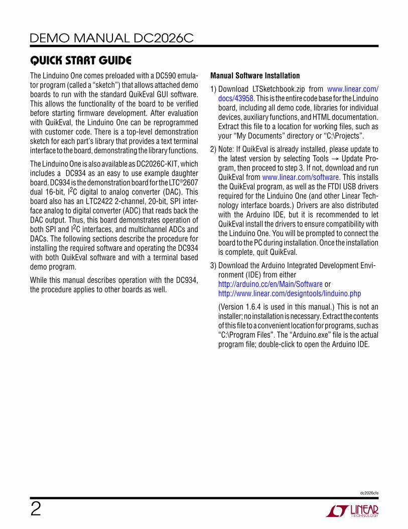
1) From within the Arduino IDE, click on File → Preferences
Under Sketchbook Location: select Browse, and locate the path to the extracted LTSketchbook.zip file. The correct location will show “LTSketchbook” in the Look In menu, and at least four subdirectories will be shown: Documenta-tion, Libraries, Part Number and Utilities (more may be added in the future). Click Open, then click OK.
4dc2026cfe
DEMO MANUAL DC2026C
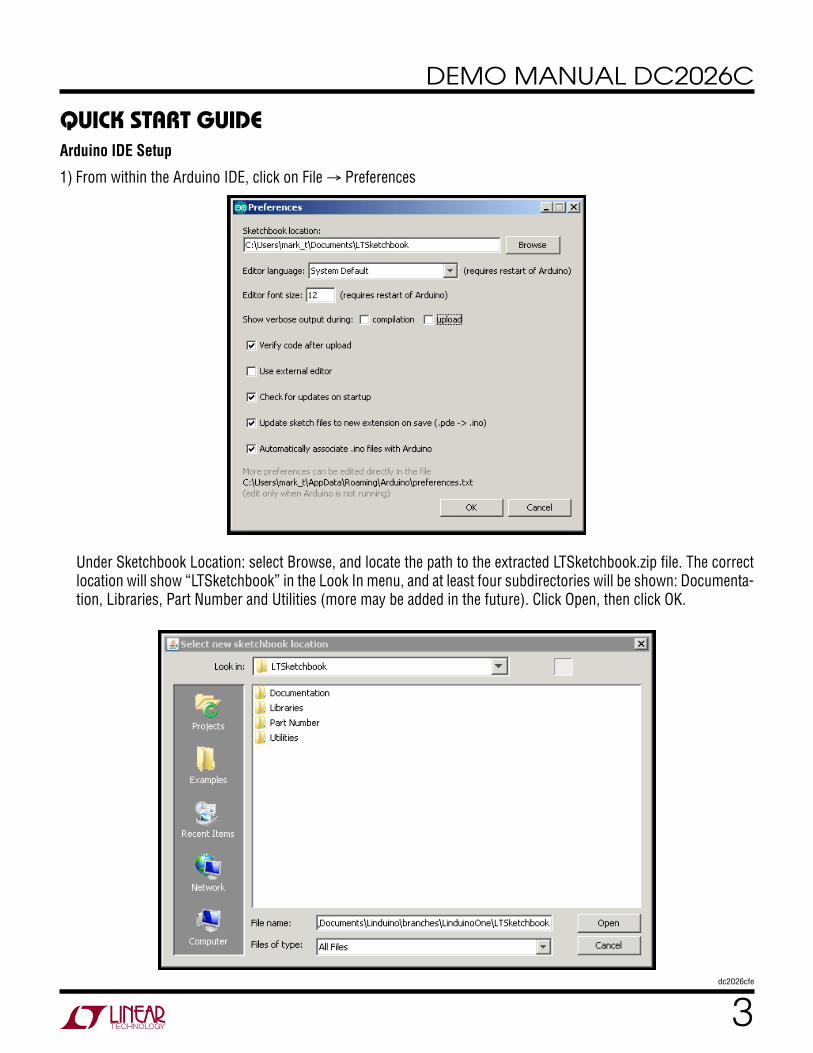
2) Under Tools menu, select Board → Arduino Uno
QUICK START GUIDE
5dc2026cfe
DEMO MANUAL DC2026C
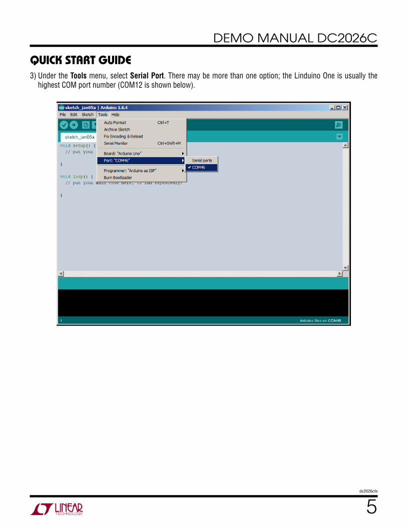
3) Under the Tools menu, select Serial Port. There may be more than one option; the Linduino One is usually the highest COM port number (COM12 is shown below).
QUICK START GUIDE
6dc2026cfe
DEMO MANUAL DC2026C
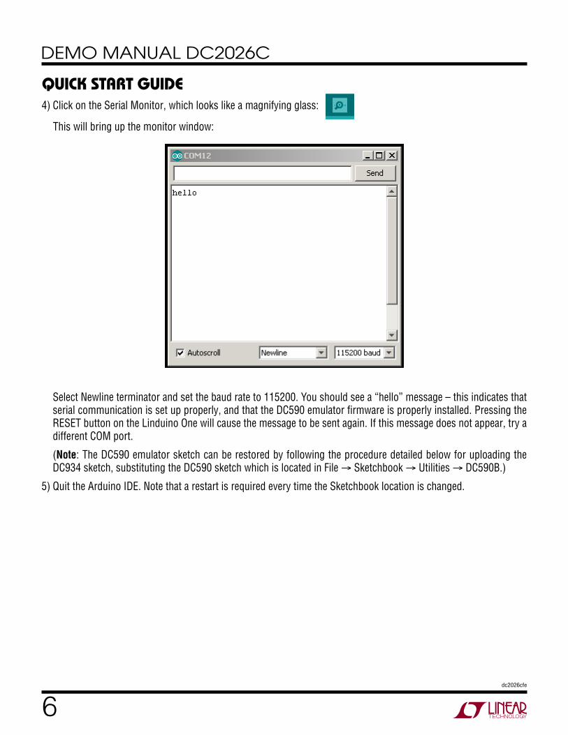
QUICK START GUIDE4) Click on the Serial Monitor, which looks like a magnifying glass:
This will bring up the monitor window:
Select Newline terminator and set the baud rate to 115200. You should see a “hello” message – this indicates that serial communication is set up properly, and that the DC590 emulator firmware is properly installed. Pressing the RESET button on the Linduino One will cause the message to be sent again. If this message does not appear, try a different COM port.
(Note: The DC590 emulator sketch can be restored by following the procedure detailed below for uploading the DC934 sketch, substituting the DC590 sketch which is located in File → Sketchbook → Utilities → DC590B.)
5) Quit the Arduino IDE. Note that a restart is required every time the Sketchbook location is changed.
7dc2026cfe
DEMO MANUAL DC2026C
QUICK START GUIDERunning with QuikEval
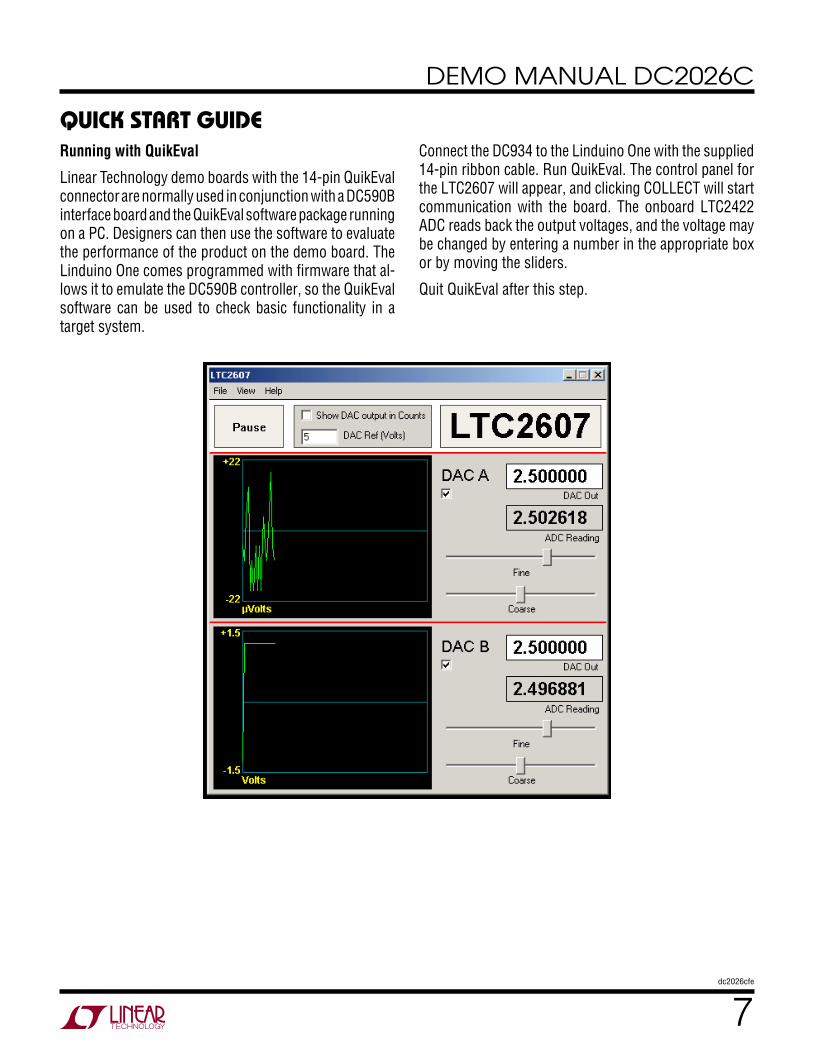
Linear Technology demo boards with the 14-pin QuikEval connector are normally used in conjunction with a DC590B interface board and the QuikEval software package running on a PC. Designers can then use the software to evaluate the performance of the product on the demo board. The Linduino One comes programmed with firmware that al-lows it to emulate the DC590B controller, so the QuikEval software can be used to check basic functionality in a target system.
Connect the DC934 to the Linduino One with the supplied 14-pin ribbon cable. Run QuikEval. The control panel for the LTC2607 will appear, and clicking COLLECT will start communication with the board. The onboard LTC2422 ADC reads back the output voltages, and the voltage may be changed by entering a number in the appropriate box or by moving the sliders.
Quit QuikEval after this step.
8dc2026cfe
DEMO MANUAL DC2026C
Running with the Linduino Demonstration Program
After the DC934 has been run with the user-friendly QuikEval GUI, a demonstration program can be loaded into the Linduino One that demonstrates the library functions for the LTC2607 and LTC2422.
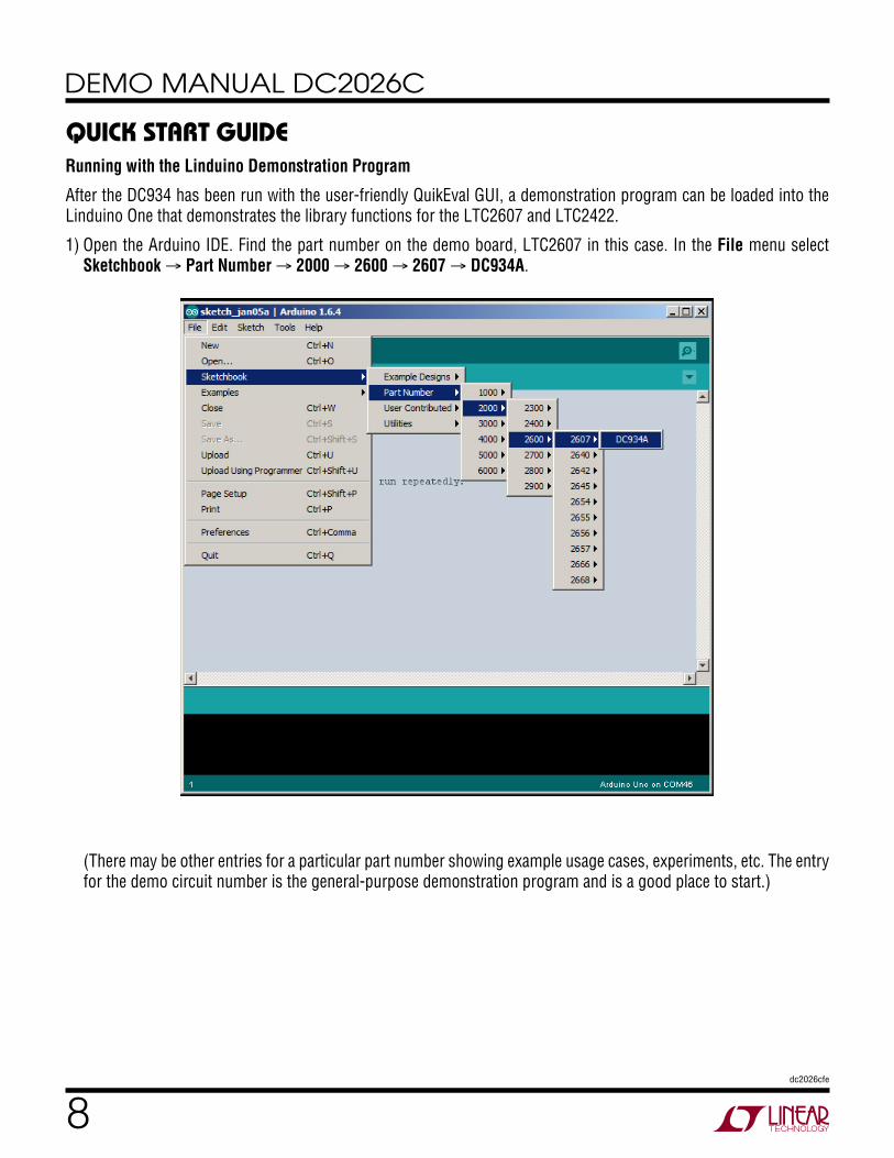
1) Open the Arduino IDE. Find the part number on the demo board, LTC2607 in this case. In the File menu select Sketchbook → Part Number → 2000 → 2600 → 2607 → DC934A.
(There may be other entries for a particular part number showing example usage cases, experiments, etc. The entry for the demo circuit number is the general-purpose demonstration program and is a good place to start.)
QUICK START GUIDE
9dc2026cfe
DEMO MANUAL DC2026C
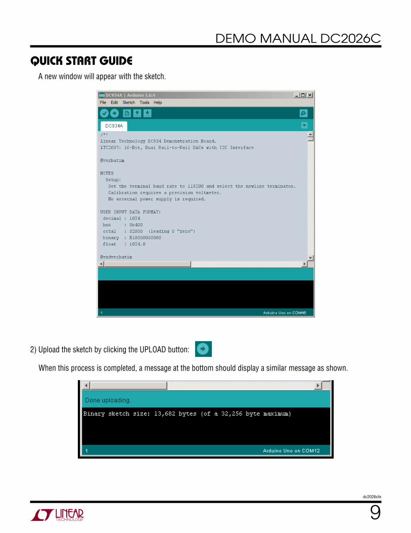
A new window will appear with the sketch.
2) Upload the sketch by clicking the UPLOAD button:
When this process is completed, a message at the bottom should display a similar message as shown.
QUICK START GUIDE
10dc2026cfe
DEMO MANUAL DC2026C
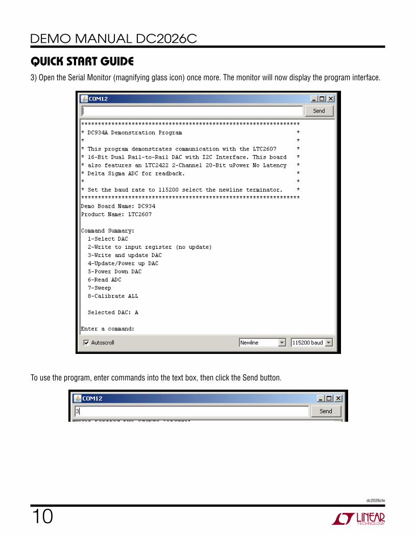
QUICK START GUIDE3) Open the Serial Monitor (magnifying glass icon) once more. The monitor will now display the program interface.
To use the program, enter commands into the text box, then click the Send button.
11dc2026cfe
DEMO MANUAL DC2026C
QUICK START GUIDEGoing Further
After completing the procedure in this Quick Start Guide, all of the tools are in place to move on to other products or further experimentation with the DC934. The main page for all Linduino resources is:
http://www.linear.com/designtools/linduino.php
HTML documentation for the code is provided in the sketchbook in the Documentation subdirectory.
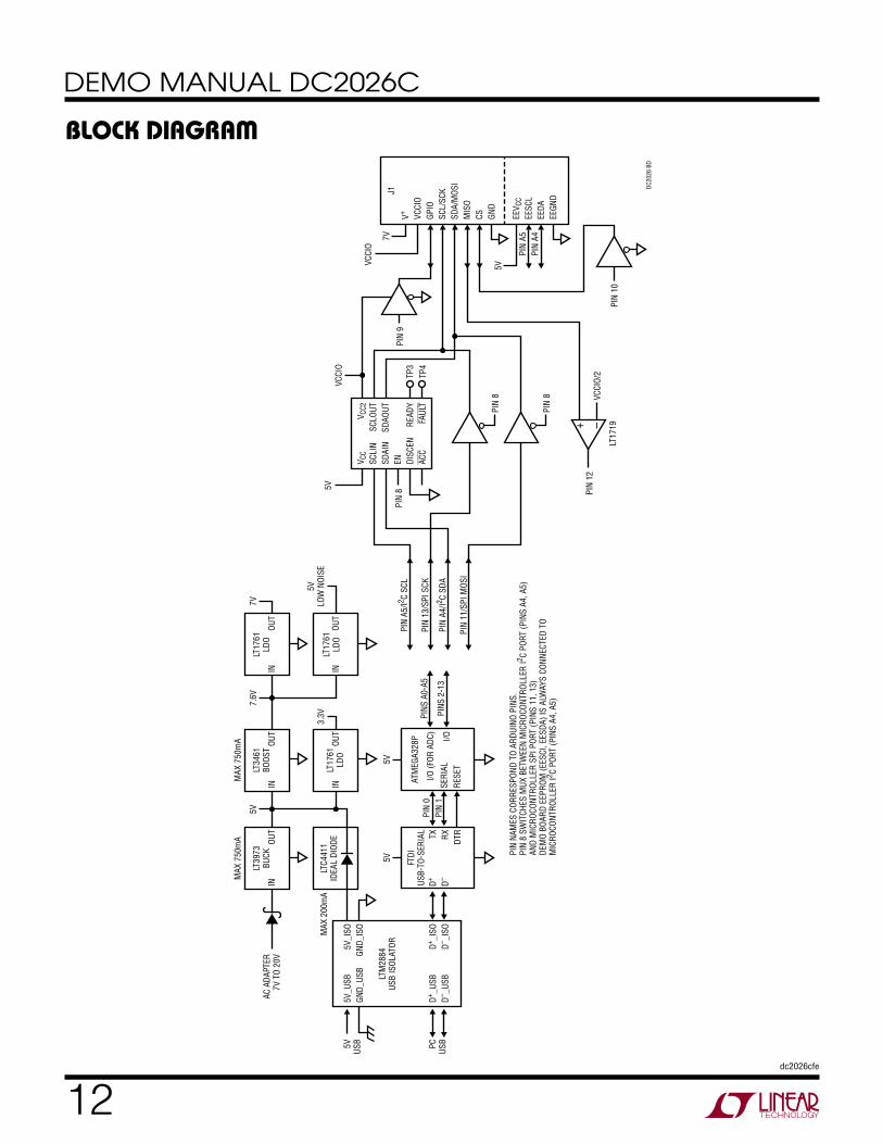
External Connections
J1: QuikEval header – Connection to QuikEval demonstra-tion board. This connector provides 5V at 50mA, 7.6V at 50mA, SPI and I2C interfaces, and an auxiliary I2C interface for identification of the attached demonstration board.
J2: AC ADAPTOR IN – 2.1mm × 5.5mm barrel connector. Optional DC power input, 7V to 20V DC. With external power applied, up to 750mA can be drawn from the 5V supply (available on pins 2 and 5 on J3, or pin 10 on J1.)
J3, J6, J7, J8: Arduino shield headers. These headers are compatible with standard Arduino “shield” add-on boards. Refer to schematic for individual signals.
J4: ICSP – In-circuit serial programming header. Used in conjunction with an external programming tool such as an AVR Dragon or JTAGICE3.
J5: USB – Connection to the host computer. Power for the Linduino and the connected daughter board is also taken from J5 if no external power is supplied to J2.
Jumpers
JP1: Factory use only.
JP2: Reset configuration, not installed. When the ICSP header is used with an external tool, install a 3 position, 0.1" header in this location and cut the trace labeled NORM on the back side of the board. Place jumper in the right-hand position (opposite to NORM) to allow the ICSP tool to control the RESET signal, install in the NORM position to allow the FT232 DTR signal to control RESET (this is normal Arduino operation, and required to program the board from within the Arduino IDE.)
JP3: VCCIO selection 5V (default), 3.3V, 2.5V, remove for 1.8V, or EXT to disable the onboard regulator and supply VCCIO to the DC2026 from the attached demo board. Refer to the documentation for the attached demo board for information on acceptable voltage levels.VCCIO is the low-voltage supply for the attached demo board. It also sets the logic level for the SPI and I2C signals.
LEDs
ON: Lights when 5V supply is on, from which all other supply voltages are generated.
SCK: Lights when Arduino pin 13 (SCK on the SPI bus) is high. This is the pin used in the “blink” sketch under File → Examples → Basics → Blink.
RX: Lights when data is being received from the host computer through the USB port.
TX: Lights when data is being sent to the host computer through the USB port.
RESET Button (S1): Asserts the ATMega328’s RESET line, restarting program execution.
12dc2026cfe
DEMO MANUAL DC2026C
BLOCK DIAGRAM
5V_U
SBGN
D_US
B
D+ _USB
D– _USB
5V_I
SOGN
D_IS
O5V
USB
AC A
DAPT
ER7V
TO
20V
MAX
200
mA
PC USB
D+ _ISO
D– _ISO
LTM
2884
USB
ISOL
ATOR
LTC4
411
IDEA
L DI
ODE
FTDI
USB-
TO-S
ERIA
L
5V
D+ D–TX RX DTR
LT39
73BU
CK
MAX
750
mA
INOU
T
LT17
61LD
O
ATM
EGA3
28P
PINS
A0-
A5
PINS
2-1
3
PIN
13/S
PI S
CK
PIN
A4/I2 C
SDA
PIN
A5/I2 C
SCL
PIN
11/S
PI M
OSI
5V
PIN
0PI
N 1
RESE
TSE
RIAL
I/O (F
OR A
DC)
I/O
LT34
61BO
OST
MAX
750
mA
INOU
T
INOU
T
3.3V
LT17
61LD
O
LT17
61LD
OIN
OUT
INOU
T
5VLO
W N
OISE
VCCI
O
VCCI
O5V
J1
5V
7V
7V7.
6V5V
V+ VCCI
OGP
IOSC
L/SC
KSD
A/M
OSI
MIS
OCS GN
D
EEV C
CEE
SCL
EEDA
EEGN
D
PIN
8
PIN
A5PI
N A4
PIN
NAM
ES C
ORRE
SPON
D TO
ARD
UINO
PIN
S.PI
N 8
SWIT
CHES
MUX
BET
WEE
N M
ICRO
CONT
ROLL
ER I2 C
PORT
(PIN
S A4
, A5)
AND
MIC
ROCO
NTRO
LLER
SPI
POR
T (P
INS
11, 1
3)DE
MO
BOAR
D EE
PROM
(EES
CI, E
ESDA
) IS
ALW
AYS
CONN
ECTE
D TO
MIC
ROCO
NTRO
LLER
I2 C PO
RT (P
INS
A4, A
5)
DC20
26 B
D
V CC
SCLI
NSD
AIN
EN DISC
ENAC
C
V CC2
SCLO
UTSD
AOUT
READ
YFAULT
TP3
TP4
PIN
8
PIN
8
PIN
12
PIN
9
+ –VC
CIO/
2
LT17
19PI
N 10
13dc2026cfe
DEMO MANUAL DC2026C
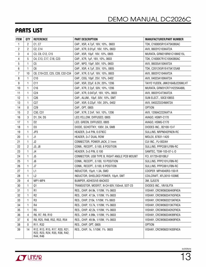
PARTS LISTITEM QTY REFERENCE PART DESCRIPTION MANUFACTURER/PART NUMBER
1 2 C1, C7 CAP., X5R, 4.7μF, 16V, 10%, 0603 TDK, C1608X5R1C475K080AC
2 2 C2, C14 CAP., X7R, 0.01μF, 16V, 10%, 0603 AVX, 0603YC103KAT2A
3 4 C3, C9, C12, C15 CAP., X5R, 10μF, 16V, 10%, 0805 MURATA, GRM21BR61C106KE15L
4 5 C4, C13, C17, C18, C23 CAP., X7R, 1μF, 16V, 10%, 0603 TDK, C1608X7R1C105K080AC
5 1 C5 CAP., NPO, 15pF, 50V, 10%, 0603 AVX, 06035A150KAT2A
6 1 C6 CAP., X5R, 4.7μF, 25V, 10%, 0805 TDK, C2012X5R1E475K125AB
7 10 C8, C19-C22, C25, C28, C32-C34 CAP., X7R, 0.1μF, 16V, 10%, 0603 AVX, 0603YC104KAT2A
8 1 C10 CAP., COG, 10pF, 25V, 10%, 0402 AVX, 04023A100KAT2A
9 1 C11 CAP., X5R, 22μF, 6.3V, 20%, 1206 TAIYO YUDEN, JMK316ABJ226MLHT
10 1 C16 CAP., X7R, 2.2μF, 50V, 10%, 1206 MURATA, GRM31CR71H225KA88L
11 1 C24 CAP., X7R, 0.047μF, 16V, 10%, 0603 AVX, 0603YC473KAT2A
12 1 C26 CAP., ALUM., 10μF, 50V, 10%, SMT SUN ELECT., 50CE10BSS
13 1 C27 CAP., X5R, 0.22μF, 10V, 20%, 0402 AVX, 0402ZD224MAT2A
14 0 C29 CAP., OPT, 0805 OPTION
15 2 C30, C31 CAP., X7R, 2.2nF, 1kV, 10%, 1206 AVX, 1206AC222KAT1A
16 3 D1, D4, D5 LED,YELLOW, DIFFUSED, 0805 AVAGO, HSMY-C170
17 1 D2 LED, GREEN, DIFFUSED, 0805 AVAGO, HSMG-C170
18 1 D3 DIODE, SCHOTTKY, 100V, 2A, SMB DIODES INC., B2100-13-F
19 1 JP3 HEADER, 2×4 PIN, 0.079CC SULLINS, NRPN042PAEN-RC
20 1 J1 HEADER, 2×7 DUAL ROW MOLEX, 87831-1420
21 1 J2 CONNECTOR, POWER JACK, 2.1mm CUI INC., PJ-002AH
22 2 J3, J8 CONN., RECEPT., 0.100, 8 POSITION SULLINS, PPPC081LFBN-RC
23 1 J4 HEADER, 2×3 PIN, 0.100 SAMTEC, TSW-103-07-L-D
24 1 J5 CONNECTOR, USB TYPE B, RIGHT ANGLE PCB MOUNT FCI, 61729-0010BLF
25 1 J6 CONN., RECEPT., 0.100, 10 POSITION SULLINS, PPPC101LFBN-RC
26 1 J7 CONN., RECEPT., 0.100, 6 POSITION SULLINS, PPPC061LFBN-RC
27 1 L1 INDUCTOR, 15μH, 1.3A, SMD COOPER MPI4040R3-150-R
28 1 L2 INDUCTOR, SHIELDED POWER, 10μH, SMT COILCRAFT, XFL3010-103ME
29 4 MP1-MP4 BUMPER, ADHESIVE-BACKED 3M, SJ5376
30 1 Q1 TRANSISTOR, MOSFET, N-CH 60V,150mA, SOT-23 DIODES INC., VN10LFTA
31 1 R1 RES., CHIP, 64.9k, 1/10W, 1% 0603 VISHAY, CRCW060364K9FKEA
32 1 R2 RES., CHIP, 47.5k, 1/10W, 1% 0603 VISHAY, CRCW060347K5FKEA
33 1 R3 RES., CHIP, 215k, 1/10W, 1% 0603 VISHAY, CRCW0603215KFKEA
34 1 R4 RES., CHIP, 13.7k, 1/10W, 1% 0603 VISHAY, CRCW060313K7FKEA
35 1 R5 RES., CHIP, 42.2k, 1/10W, 1% 0603 VISHAY, CRCW060342K2FKEA
36 4 R6, R7, R9, R10 RES., CHIP, 4.99k, 1/10W, 1% 0603 VISHAY, CRCW06034K99FKEA
37 6 R8, R25, R48, R52, R53, R54 RES., CHIP, 49.9k, 1/10W, 1% 0603 VISHAY, CRCW060349K9FKEA
38 0 R11, R32 RES., CHIP, OPT, 0805 OPTION
39 14 R12, R13, R15, R17, R20, R21, R22, R23, R24, R35, R36, R42, R44, R46
RES., CHIP, 1k, 1/10W, 1% 0603 VISHAY, CRCW06031K00FKEA
14dc2026cfe
DEMO MANUAL DC2026C
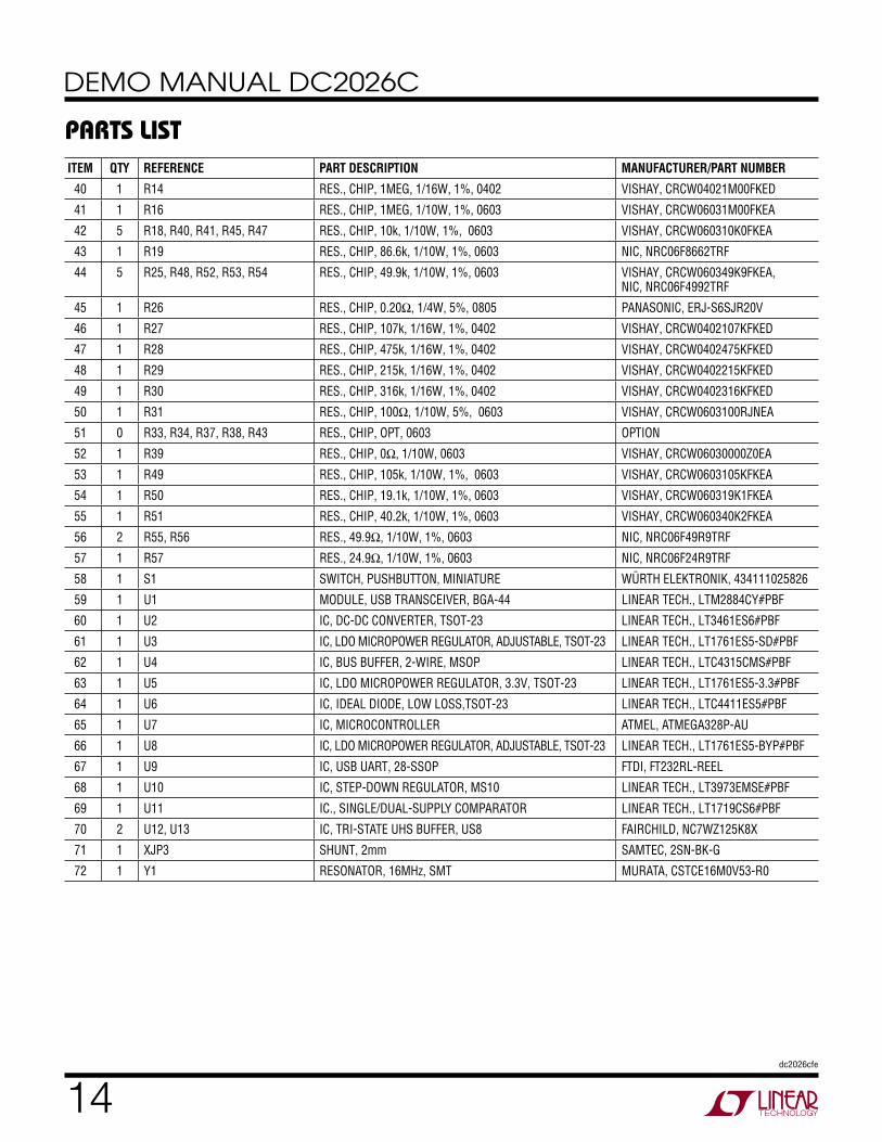
PARTS LISTITEM QTY REFERENCE PART DESCRIPTION MANUFACTURER/PART NUMBER
40 1 R14 RES., CHIP, 1MEG, 1/16W, 1%, 0402 VISHAY, CRCW04021M00FKED
41 1 R16 RES., CHIP, 1MEG, 1/10W, 1%, 0603 VISHAY, CRCW06031M00FKEA
42 5 R18, R40, R41, R45, R47 RES., CHIP, 10k, 1/10W, 1%, 0603 VISHAY, CRCW060310K0FKEA
43 1 R19 RES., CHIP, 86.6k, 1/10W, 1%, 0603 NIC, NRC06F8662TRF
44 5 R25, R48, R52, R53, R54 RES., CHIP, 49.9k, 1/10W, 1%, 0603 VISHAY, CRCW060349K9FKEA, NIC, NRC06F4992TRF
45 1 R26 RES., CHIP, 0.20Ω, 1/4W, 5%, 0805 PANASONIC, ERJ-S6SJR20V
46 1 R27 RES., CHIP, 107k, 1/16W, 1%, 0402 VISHAY, CRCW0402107KFKED
47 1 R28 RES., CHIP, 475k, 1/16W, 1%, 0402 VISHAY, CRCW0402475KFKED
48 1 R29 RES., CHIP, 215k, 1/16W, 1%, 0402 VISHAY, CRCW0402215KFKED
49 1 R30 RES., CHIP, 316k, 1/16W, 1%, 0402 VISHAY, CRCW0402316KFKED
50 1 R31 RES., CHIP, 100Ω, 1/10W, 5%, 0603 VISHAY, CRCW0603100RJNEA
51 0 R33, R34, R37, R38, R43 RES., CHIP, OPT, 0603 OPTION
52 1 R39 RES., CHIP, 0Ω, 1/10W, 0603 VISHAY, CRCW06030000Z0EA
53 1 R49 RES., CHIP, 105k, 1/10W, 1%, 0603 VISHAY, CRCW0603105KFKEA
54 1 R50 RES., CHIP, 19.1k, 1/10W, 1%, 0603 VISHAY, CRCW060319K1FKEA
55 1 R51 RES., CHIP, 40.2k, 1/10W, 1%, 0603 VISHAY, CRCW060340K2FKEA
56 2 R55, R56 RES., 49.9Ω, 1/10W, 1%, 0603 NIC, NRC06F49R9TRF
57 1 R57 RES., 24.9Ω, 1/10W, 1%, 0603 NIC, NRC06F24R9TRF
58 1 S1 SWITCH, PUSHBUTTON, MINIATURE WÜRTH ELEKTRONIK, 434111025826
59 1 U1 MODULE, USB TRANSCEIVER, BGA-44 LINEAR TECH., LTM2884CY#PBF
60 1 U2 IC, DC-DC CONVERTER, TSOT-23 LINEAR TECH., LT3461ES6#PBF
61 1 U3 IC, LDO MICROPOWER REGULATOR, ADJUSTABLE, TSOT-23 LINEAR TECH., LT1761ES5-SD#PBF
62 1 U4 IC, BUS BUFFER, 2-WIRE, MSOP LINEAR TECH., LTC4315CMS#PBF
63 1 U5 IC, LDO MICROPOWER REGULATOR, 3.3V, TSOT-23 LINEAR TECH., LT1761ES5-3.3#PBF
64 1 U6 IC, IDEAL DIODE, LOW LOSS,TSOT-23 LINEAR TECH., LTC4411ES5#PBF
65 1 U7 IC, MICROCONTROLLER ATMEL, ATMEGA328P-AU
66 1 U8 IC, LDO MICROPOWER REGULATOR, ADJUSTABLE, TSOT-23 LINEAR TECH., LT1761ES5-BYP#PBF
67 1 U9 IC, USB UART, 28-SSOP FTDI, FT232RL-REEL
68 1 U10 IC, STEP-DOWN REGULATOR, MS10 LINEAR TECH., LT3973EMSE#PBF
69 1 U11 IC., SINGLE/DUAL-SUPPLY COMPARATOR LINEAR TECH., LT1719CS6#PBF
70 2 U12, U13 IC, TRI-STATE UHS BUFFER, US8 FAIRCHILD, NC7WZ125K8X
71 1 XJP3 SHUNT, 2mm SAMTEC, 2SN-BK-G
72 1 Y1 RESONATOR, 16MHz, SMT MURATA, CSTCE16M0V53-R0
15dc2026cfe
DEMO MANUAL DC2026C
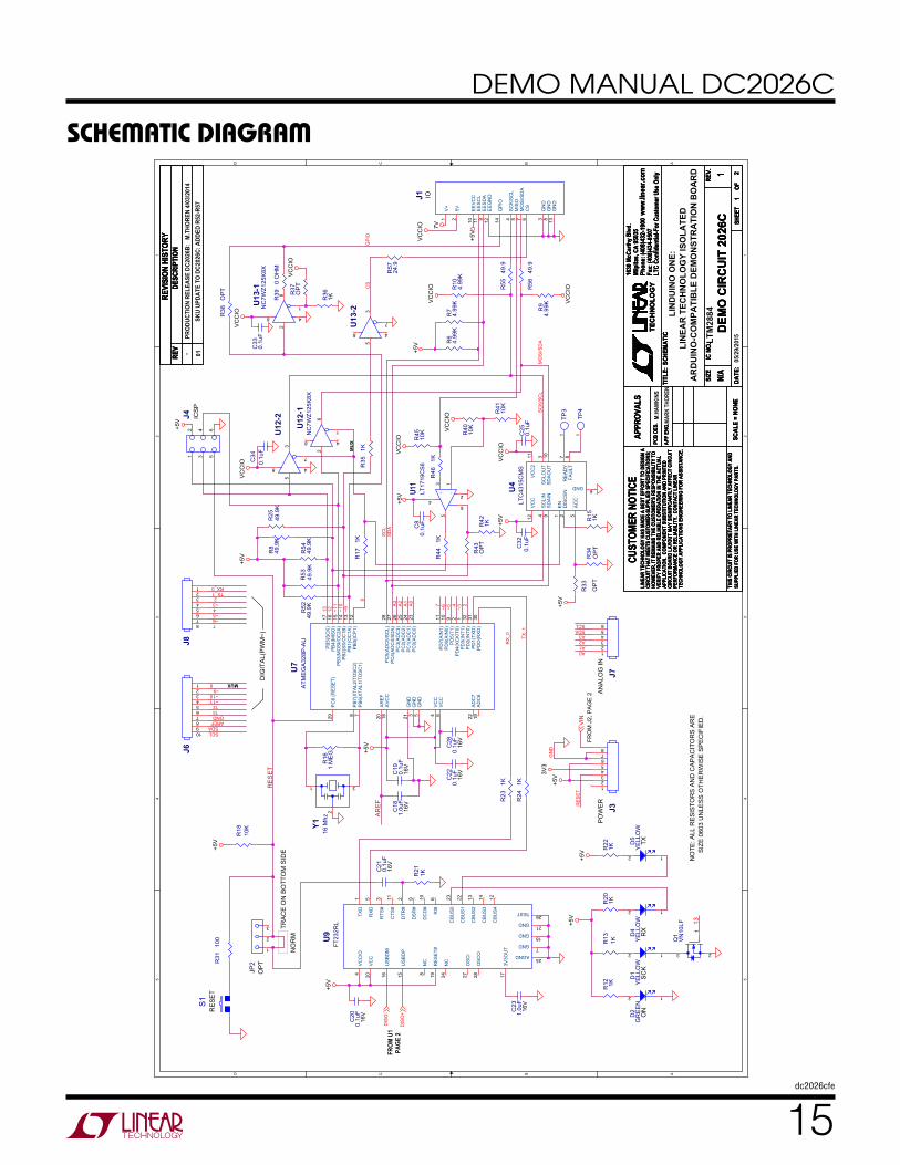
SCHEMATIC DIAGRAM5 5
4 4
3 3
2 2
1 1
DD
CC
BB
AA
LTM
2884
AN
ALO
G IN
NO
RM
ICS
P
NO
TE: A
LL R
ES
ISTO
RS
AN
D C
AP
AC
ITO
RS
AR
ES
IZE
060
3 U
NLE
SS
OTH
ER
WIS
E S
PE
CIF
IED
.
M.HA
WKI
NSMA
RK T
HORE
N
OP
T
FROM
U1
DIG
ITA
L(P
WM
~)
PO
WE
R
SC
K
FRO
M J
2, P
AG
E 2
TXR
XO
N
IO
PAGE
2
MUX
RE
SE
T
TRA
CE
ON
BO
TTO
M S
IDE
MU
X
LIN
EAR
TEC
HN
OLO
GY
ISO
LATE
DA
RD
UIN
O-C
OM
PATI
BLE
DEM
ON
STR
ATI
ON
BO
AR
D
LIN
DU
INO
ON
E:
05/2
9/20
15
-PR
ODUC
TION
REL
EASE
DC2
026B
: M
.THO
REN
4/03
/201
401
SKU
UPDA
TE T
O DC
2026
C: A
DDED
R52
-R57
A0
A1
A2
A3
7~6 ~5
4~3
2
AR
EF
~11
~9
RX
_0
RE
SE
T
TX_1
SCLSDA
AREFGND
1312~11~10~9
8
7~6~54
~32
TX_1RX_0
SCLSDAA3A2A1A0
GN
D
RE
SE
T
13
13
SC
K/S
CL
MO
SI/S
DA
GP
IOC
S
SC
LS
DA
~10
12
8+5
V
+5V
+5V
+5V
VC
CIO 7V
+5V
+5V3V
3
+5V
+5V
+5V
VC
CIO
VC
CIO
+5V
VC
CIO
+5V
+5V
VC
CIO
VC
CIO
+5V
VC
CIO
VC
CIO
VC
CIO
DIS
O-
DIS
O+
VIN
SIZE
DATE
:
IC N
O.RE
V.
SHEE
TOF
TITL
E:
APPR
OVAL
S
PCB
DES.
APP
ENG.
TEC
HN
OLO
GY
Fax:
(408
)434
-050
7
Milp
itas,
CA 95
035
Phon
e: (4
08)4
32-1
900
1630
McC
arth
y Blvd
.
LTC
Conf
iden
tial-F
or C
usto
mer
Use
Onl
y
CUST
OMER
NOT
ICE
LINE
AR T
ECHN
OLOG
Y HA
S MA
DE A
BES
T EF
FORT
TO
DESI
GN A
CIRC
UIT
THAT
MEE
TS C
USTO
MER-
SUPP
LIED
SPE
CIFI
CATI
ONS;
HOW
EVER
, IT R
EMAI
NS T
HE C
USTO
MER'
S RE
SPON
SIBI
LITY
TO
VERI
FY P
ROPE
R AN
D RE
LIAB
LE O
PERA
TION
IN T
HE A
CTUA
LAP
PLIC
ATIO
N. C
OMPO
NENT
SUB
STIT
UTIO
N AN
D PR
INTE
DCI
RCUI
T BO
ARD
LAYO
UT M
AY S
IGNI
FICA
NTLY
AFF
ECT
CIRC
UIT
PERF
ORMA
NCE
OR R
ELIA
BILI
TY. C
ONTA
CT L
INEA
RTE
CHNO
LOGY
APP
LICA
TION
S EN
GINE
ERIN
G FO
R AS
SIST
ANCE
.
THIS
CIR
CUIT
IS P
ROPR
IETA
RY T
O LI
NEAR
TEC
HNOL
OGY
AND
SCHE
MAT
IC
SUPP
LIED
FOR
USE
WIT
H LI
NEAR
TEC
HNOL
OGY
PART
S.SC
ALE
= NO
NE
www.
linea
r.com 1
DEM
O C
IRC
UIT
202
6C1
2
N/A
REVI
SION
HIS
TORY
DESC
RIPT
ION
REV
REVI
SION
HIS
TORY
DESC
RIPT
ION
REV
REVI
SION
HIS
TORY
DESC
RIPT
ION
REV
R31
100
U7
ATM
EG
A32
8P-A
U
PC
6 (R
ES
ET)
29
PB
6(X
TAL1
/TO
SC
1)7
AR
EF
20
GN
D5
GN
D3
AV
CC
18
GN
D21
PB
7(X
TAL2
/TO
SC
2)8
VC
C4
VC
C6
AD
C7
22
AD
C6
19P
DO
(RX
D)
30P
D1(
TXD
)31
PD
2(IN
T0)
32P
D3(
INT1
)1
PD
4(X
CK
/T0)
2P
D5(
T1)
9P
D6(
AIN
0)10
PD
7(A
IN1)
11
PC
0(A
DC
0)23
PC
1(A
DC
1)24
PC
2(A
DC
2)25
PC
3(A
DC
3)26
PC
4(A
DC
4/S
DA
)27
PC
5(A
DC
5/S
CL)
28
PB
0(IC
P1)
12P
B1(
OC
1A)
13P
B2(
SS
/OC
1B)
14P
B3(
MO
SI/O
C2A
)15
PB
4(M
ISO
)16
PB
5(S
CK
)17
R42
1K
C21
0.1u
F16
V
R55
49.9
R41
10K
U12
-1N
C7W
Z125
K8X
6
8 4
2
1
D5
YE
LLO
W
2 1
C33
0.1u
F
R25
49.9
K
R10
4.99
K
R6
4.99
K
C20
0.1u
F16
V
R9
4.99
K
S1
R45
10K
C28
0.1u
F16
V
D4
YE
LLO
W
2 1
R44
1K
R16
1 M
EG
D1
YE
LLO
W
2 1
U13
-2 3
8 4
5
7
R18
10K
C23
1.0u
F16
V
R35
1K
C34
0.1u
F
R37
OP
T
R12 1K
JP2
1
3
2
J1
V+
1
GN
D3
MIS
O5
MO
SI/S
DA
7
EE
SD
A9
EE
SC
L11
GN
D13
5V2
SC
K/S
CL
4
CS
6
GN
D8
EE
VC
C10
EE
GN
D12
GP
IO14
C19
0.1u
F16
V
C32
0.1u
F
R34
OP
T
Y116
Mhz
1 3
2
R17
1K
R8
49.9
K
+ -U11
LT17
19C
S6
3 15
42
6
U9
FT23
2RL
TXD
1
RX
D5
RTS
#3
CTS
#11
DTR
#2
DS
R#
9
DC
D#
10
RI#
6
CB
US
023
CB
US
122
CB
US
213
CB
US
314
CB
US
412
TEST26
GND21
GND18
GND7
AGND25
VC
CIO
4
VC
C20
US
BD
M16
US
BD
P15
NC
8
RE
SE
T#19
NC
24
OS
CI
27
OS
CO
28
3V3O
UT
17
R36
1K
R33
OP
T
R23
1K
R39
0 O
HM
U13
-1N
C7W
Z125
K8X
6
8 4
2
1
R21
1K
J7
123456
J6
123456789
10
R38
OP
T
J41 3 5
642
D2
GR
EE
N
2 1
R46
1K
U12
-23
8 4
5
7
R22
1K
R24
1K
TP4
1
R13
1K
C8
0.1u
F
R56
49.9
U4
LTC
4315
CM
S
EN
1
GND6
RE
AD
Y7
DIS
CE
N2
SC
LOU
T3
AC
C5
SC
LIN
4
FAU
LT8
SD
AIN
9S
DA
OU
T10
VC
C2
11V
CC
12 R15
1K
TP3
1
R20
1K
R7
4.99
K
R53
49.9
KR
5449
.9K
C25
0.1u
F
J8
12345678
C18
1.0u
F16
V
R52
49.9
K
J3
12345678
R57
24.9
R40
10K
Q1
VN
10LF
1
23
R43
OP
T
C22
0.1u
F16
V
16dc2026cfe
DEMO MANUAL DC2026C
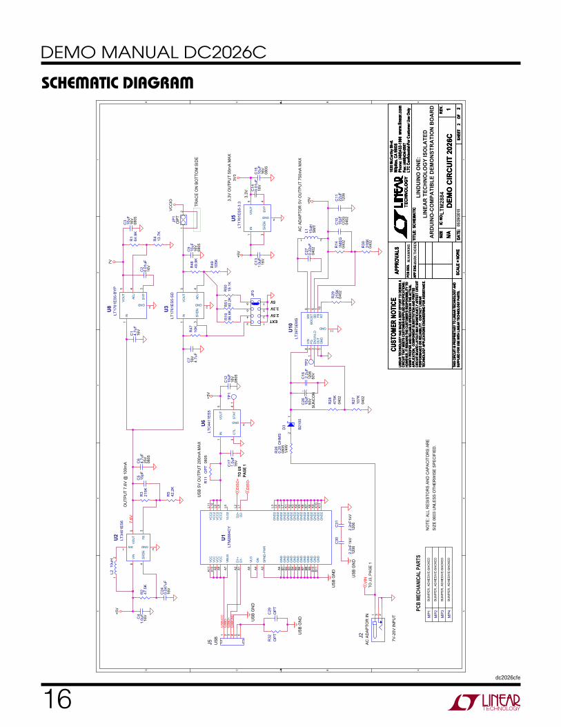
SCHEMATIC DIAGRAM5 5
4 4
3 3
2 2
1 1
DD
CC
BB
AA
3.3V
AC
AD
AP
TOR
IN
US
B G
ND
US
B
US
B G
ND
NO
TE: A
LL R
ES
ISTO
RS
AN
D C
AP
AC
ITO
RS
AR
E
SIZ
E 0
603
UN
LES
S O
THE
RW
ISE
SP
EC
IFIE
D.
TO U
9PA
GE 1
TO J
3, P
AG
E 1
OP
T
TRA
CE
ON
BO
TTO
M S
IDE
US
B G
ND
US
B G
ND
OU
TPU
T 7.
6V @
100
mA
3.3V
OU
TPU
T 50
mA
MA
X
AC
AD
AP
TOR
5V
OU
TPU
T 75
0mA
MA
X
US
B 5
V O
UTP
UT
200m
A M
AX
7V-2
0V IN
PU
T
5V3.3V2.5VEXT
PCB
MECH
ANIC
AL P
ARTS
M.HA
WKI
NSMA
RK T
HORE
N
05/2
9/20
15
LIN
EAR
TEC
HN
OLO
GY
ISO
LATE
DA
RD
UIN
O-C
OM
PATI
BLE
DEM
ON
STR
ATI
ON
BO
AR
D
LIN
DU
INO
ON
E:
LTM
2884
7.6V
US
BD
-U
SB
D+
US
BV
CC
US
BG
ND+5
V
+5V
3V3
+5V
7V
+5V
VC
CIO
DIS
O+
DIS
O-
VIN
SIZE
DATE
:
IC N
O.RE
V.
SHEE
TOF
TITL
E:
APPR
OVAL
S
PCB
DES.
APP
ENG.
TEC
HN
OLO
GY
Fax:
(408
)434
-050
7
Milp
itas,
CA 95
035
Phon
e: (4
08)4
32-1
900
1630
McC
arth
y Blvd
.
LTC
Conf
iden
tial-F
or C
usto
mer
Use
Onl
y
CUST
OMER
NOT
ICE
LINE
AR T
ECHN
OLOG
Y HA
S MA
DE A
BES
T EF
FORT
TO
DESI
GN A
CIRC
UIT
THAT
MEE
TS C
USTO
MER-
SUPP
LIED
SPE
CIFI
CATI
ONS;
HOW
EVER
, IT R
EMAI
NS T
HE C
USTO
MER'
S RE
SPON
SIBI
LITY
TO
VERI
FY P
ROPE
R AN
D RE
LIAB
LE O
PERA
TION
IN T
HE A
CTUA
LAP
PLIC
ATIO
N. C
OMPO
NENT
SUB
STIT
UTIO
N AN
D PR
INTE
DCI
RCUI
T BO
ARD
LAYO
UT M
AY S
IGNI
FICA
NTLY
AFF
ECT
CIRC
UIT
PERF
ORMA
NCE
OR R
ELIA
BILI
TY. C
ONTA
CT L
INEA
RTE
CHNO
LOGY
APP
LICA
TION
S EN
GINE
ERIN
G FO
R AS
SIST
ANCE
.
THIS
CIR
CUIT
IS P
ROPR
IETA
RY T
O LI
NEAR
TEC
HNOL
OGY
AND
SCHE
MAT
IC
SUPP
LIED
FOR
USE
WIT
H LI
NEAR
TEC
HNOL
OGY
PART
S.SC
ALE
= NO
NE
www.
linea
r.com 1
DEM
O C
IRC
UIT
202
6C2
2
N/A
MP
1B
UM
PE
R, A
DH
ES
IVE
-BA
CK
ED
R14
1ME
G04
02
TP1
1
D3
B21
00
21
C15
10uF
16V
0805
R28
475K
0402
MP
4B
UM
PE
R, A
DH
ES
IVE
-BA
CK
ED
R11
OP
T08
05
R32
OP
T
R4
13.7
K
C9
10uF
16V
0805
R47
10K
J5
1 2 3 4 5 6
R3
215K
U6
LTC
4411
ES
5
GND2
STA
T4
IN1
VO
UT
5
CTL
3
C14
0.01
uF16
V
R26
0.20
OH
MS
0805
1/4W
+C
2610
uF50
VS
UN
CO
N
C12
10uF
16V
0805
C4
1.0u
F16
V
C24
0.04
7uF
16V
C17
1.0u
F16
V
MP
2B
UM
PE
R, A
DH
ES
IVE
-BA
CK
ED
C7
4.7u
F16
V
C16 2.2u
F12
0650
V
R5
42.2
K
C27
0.22
uF04
02
R50
19.1
K
U8
LT17
61E
S5-
BY
P
GND2
BY
P3
IN1
VO
UT
5
AD
J4
R1
64.9
K
C10
10pF
CO
G04
02
C11
22uF
1206
U3
LT17
61E
S5-
SD
GND2
SH
DN
3
IN1
VO
UT
5
AD
J4
U5
LT17
61E
S5-
3.3
GND2
BY
P4
IN1
VO
UT
5
SH
DN
3
JP3
1
3
56
4
2
78
C31
2.2n
F1k
V12
06
C2
0.01
uF16
V
R30
316K
0402
R2
47.5
K
C3
10uF
16V
0805
L210
uH1
2
J2
231 MP
3B
UM
PE
R, A
DH
ES
IVE
-BA
CK
ED
TP2
1
R27
107K
0402
R48
49.9
K
C30
2.2n
F1k
V12
06
C6
4.7u
F25
V08
05
L1 15uH
SM
T
1 2
R51
40.2
K R29
215K
0402
C13
1.0u
F16
V
C29
OP
T
U10
LT39
73E
MS
PG
9
RT
10
BO
OS
T7
EN
/UV
LO3
OU
T2
GND11
GN
D5
VIN
4
FB1
BD
8S
W6
U2
LT34
61E
S6
SW1
GND2
FB3
VIN
6
SH
DN
4
VO
UT
5
R49
105K
C1
4.7u
F16
V
R19
86.6
K
JP1
12
C5
15pF
U1
LTM
2884
CY
D1+
A2
D1-
A1
SP
ND
-PW
RA
3O
NA
4V
LOA
5
GN
DB
1
GN
DB
2
GN
DB
3
GN
DB
4
GN
DB
5
GN
DB
6
GN
DB
7
GN
DB
8
GN
DB
9
GN
DB
10
GN
DB
11
GN
D2
K1
GN
D2
K2
GN
D2
K3
GN
D2
K4
GN
D2
K5
GN
D2
K6
GN
D2
K7
GN
D2
K8
GN
D2
K9
GN
D2
K10
GN
D2
K11
GN
D2
L3
GN
D2
L4
GN
D2
L6
GN
D2
L7G
ND
A6
VB
US
A7
VC
CA
8V
CC
A9
VC
CA
10V
CC
A11
D2-
L1D
2+L2
VLO
2L5
VC
C2
L8V
CC
2L9
VC
C2
L10
VC
C2
L11
17dc2026cfe
DEMO MANUAL DC2026C
Information furnished by Linear Technology Corporation is believed to be accurate and reliable. However, no responsibility is assumed for its use. Linear Technology Corporation makes no representa-tion that the interconnection of its circuits as described herein will not infringe on existing patent rights.
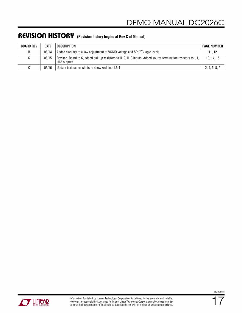
REVISION HISTORYBOARD REV DATE DESCRIPTION PAGE NUMBER
B 08/14 Added circuitry to allow adjustment of VCCIO voltage and SPI/I2C logic levels 11, 12
C 06/15 Revised Board to C, added pull-up resistors to U12, U13 inputs. Added source termination resistors to U1, U13 outputs.
13, 14, 15
C 03/16 Update text, screenshots to show Arduino 1.6.4 2, 4, 5, 8, 9
(Revision history begins at Rev C of Manual)
18dc2026cfe
DEMO MANUAL DC2026C
Linear Technology Corporation1630 McCarthy Blvd., Milpitas, CA 95035-7417 (408) 432-1900 FAX: (408) 434-0507 www.linear.com LINEAR TECHNOLOGY CORPORATION 2013
LT 0316 REV E • PRINTED IN USA
DEMONSTRATION BOARD IMPORTANT NOTICE
Linear Technology Corporation (LTC) provides the enclosed product(s) under the following AS IS conditions:
This demonstration board (DEMO BOARD) kit being sold or provided by Linear Technology is intended for use for ENGINEERING DEVELOPMENT OR EVALUATION PURPOSES ONLY and is not provided by LTC for commercial use. As such, the DEMO BOARD herein may not be complete in terms of required design-, marketing-, and/or manufacturing-related protective considerations, including but not limited to product safety measures typically found in finished commercial goods. As a prototype, this product does not fall within the scope of the European Union directive on electromagnetic compatibility and therefore may or may not meet the technical requirements of the directive, or other regulations.
If this evaluation kit does not meet the specifications recited in the DEMO BOARD manual the kit may be returned within 30 days from the date of delivery for a full refund. THE FOREGOING WARRANTY IS THE EXCLUSIVE WARRANTY MADE BY THE SELLER TO BUYER AND IS IN LIEU OF ALL OTHER WARRANTIES, EXPRESSED, IMPLIED, OR STATUTORY, INCLUDING ANY WARRANTY OF MERCHANTABILITY OR FITNESS FOR ANY PARTICULAR PURPOSE. EXCEPT TO THE EXTENT OF THIS INDEMNITY, NEITHER PARTY SHALL BE LIABLE TO THE OTHER FOR ANY INDIRECT, SPECIAL, INCIDENTAL, OR CONSEQUENTIAL DAMAGES.
The user assumes all responsibility and liability for proper and safe handling of the goods. Further, the user releases LTC from all claims arising from the handling or use of the goods. Due to the open construction of the product, it is the user’s responsibility to take any and all appropriate precautions with regard to electrostatic discharge. Also be aware that the products herein may not be regulatory compliant or agency certified (FCC, UL, CE, etc.).
No License is granted under any patent right or other intellectual property whatsoever. LTC assumes no liability for applications assistance, customer product design, software performance, or infringement of patents or any other intellectual property rights of any kind.
LTC currently services a variety of customers for products around the world, and therefore this transaction is not exclusive.
Please read the DEMO BOARD manual prior to handling the product. Persons handling this product must have electronics training and observe good laboratory practice standards. Common sense is encouraged.
This notice contains important safety information about temperatures and voltages. For further safety concerns, please contact a LTC applica-tion engineer.
Mailing Address:
Linear Technology
1630 McCarthy Blvd.
Milpitas, CA 95035
Copyright © 2004, Linear Technology Corporation