Embed Size (px)
Citation preview
DC/DC Converter with Transparent Electronics for application on Photovoltaic Panels
Romano Torres19th July 2013 1
Supervisor: Vitor Grade TavaresSecond Supervisor: Pedro Miguel Cândido BarquinhaSecond Supervisor: Pydi Ganga Bahubalindruni
Master of Electrical and Computers Engineering
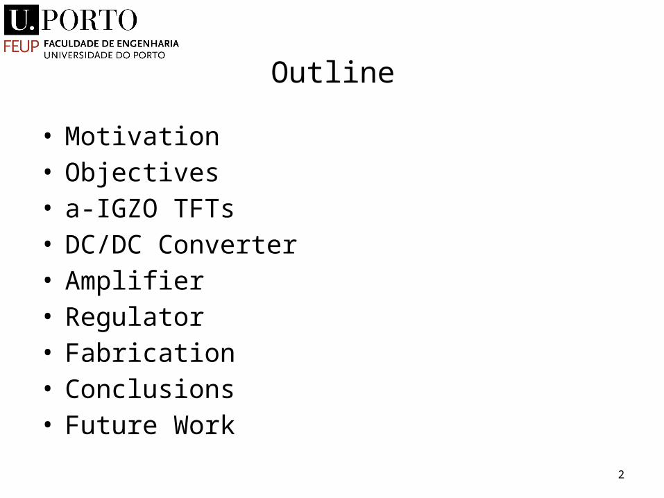
Outline
• Motivation• Objectives• a-IGZO TFTs• DC/DC Converter• Amplifier• Regulator• Fabrication• Conclusions• Future Work
2

Motivation
• To construct circuits on flexible substracts, such as plastic, glass:– Possible to embody in photovoltaic panels.
• Low cost fabrication at room temperature.
3

Objectives
• Design of a boost DC/DC converter using transparent electronics in order to have an increased and stable voltage level with direct current.– Vout > 1.5*Vin;– Efficiency >= 40%
• Fabrication of the circuit in CENIMAT/UNL.
4

a-IGZO TFTs
• High parasitic resistance;
• P-type transistors with low performance;
• Threshold voltage shift.
5Staggered bottom-gate TFT structure
Problems:
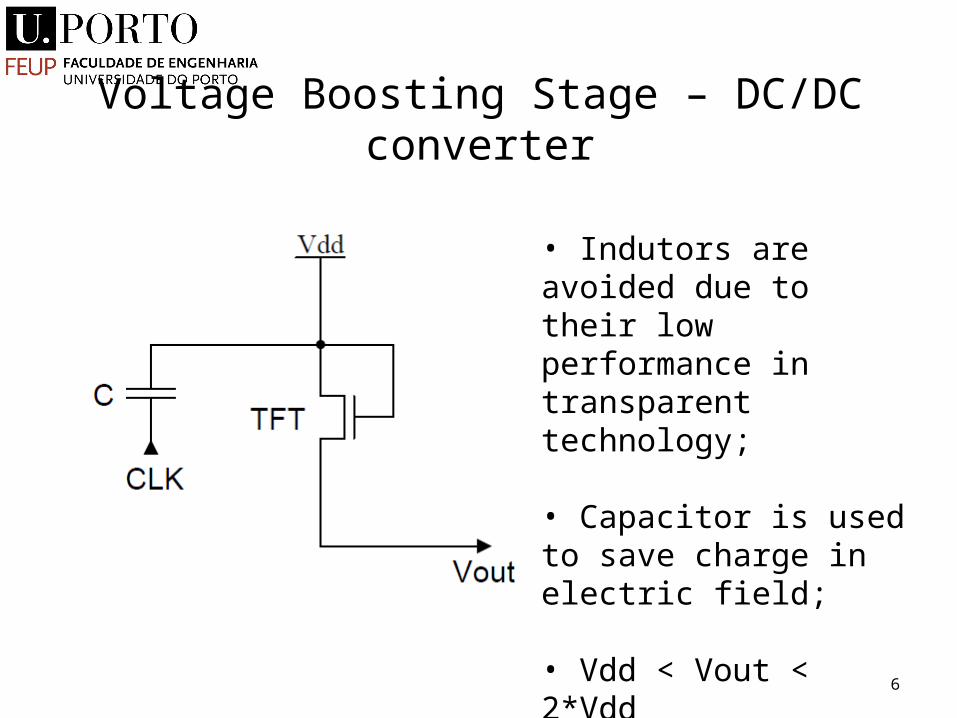
Voltage Boosting Stage – DC/DC converter
6
• Indutors are avoided due to their low performance in transparent technology;
• Capacitor is used to save charge in electric field;
• Vdd < Vout < 2*Vdd

Voltage Boosting Stage - out of phase clock signals
7Lower variation of Vout level.

2 Voltage Boosting Stages in Cascade
8
• To increase the voltage level twice;
• Parasitic effects reduce the efficiency;
• 4 TFTs of 320 μm in parallel for each diode-connection are used;
• Vdd < Vout << 3*Vdd

Separation between Boosting Stages
9
• Allow a stable voltage level at node E;
• Avoid clock feedthrough in TFT1 and TFT2.

3 Boosting Stages in Cascade
10
• Proposed DC/DC converter includes 3 Voltage Boosting Stages;
• Settling time is increased.

Bootstrapping Stage – Proposed DC/DC converter
11
• Bootstrapping stage is used to reduce the settling time of the circuit;
• Power consumption is negligble;
• Small capacitors and transistors can be used.

Comparison with previous DC/DC converters in the same technology
12
DC/DC converter from other authors Proposed DC/DC converter

DC/DC Converter - Simulation
13
Output voltage
With Load
I_load = 162 μAVout=16.37 V
Without Load
Vout=35.5 V
Bootstrapping
Cross-connected

Efficiency
• The supplied current of each voltage source is measured (I_in=167 μA);
• The currents multiplied by the supplied voltage (Vin=10V) are added, resulting in the input power;
• With the same current for each voltage source, efficiency is:
• The current supplied in bootstrapping stage is very low (I_bs=0.12μA);
• The efficiency is: 39.93%
14

3 Voltage Boosting Stages - Simulation
15
Voltage levels for each stage

DC/DC converter - Layout
165793.55 μm
3068.55 μm

10 DC/DC converters in parallel
- The equivalent resistance of 10 converters in parallel is lower than with only one converter.
17
Output voltage
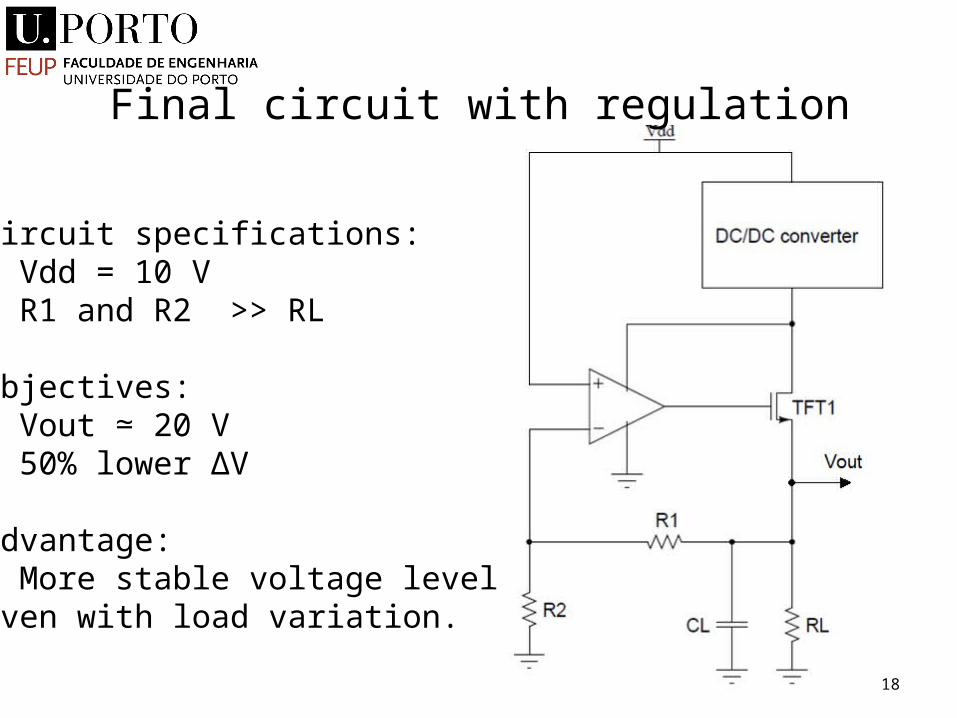
Final circuit with regulation
18
Circuit specifications:• Vdd = 10 V• R1 and R2 >> RL
Objectives:• Vout 20 V≃• 50% lower ΔV
Advantage:• More stable voltage leveleven with load variation.

Proposed Amplifier – Block diagram
19

Amplifier
20
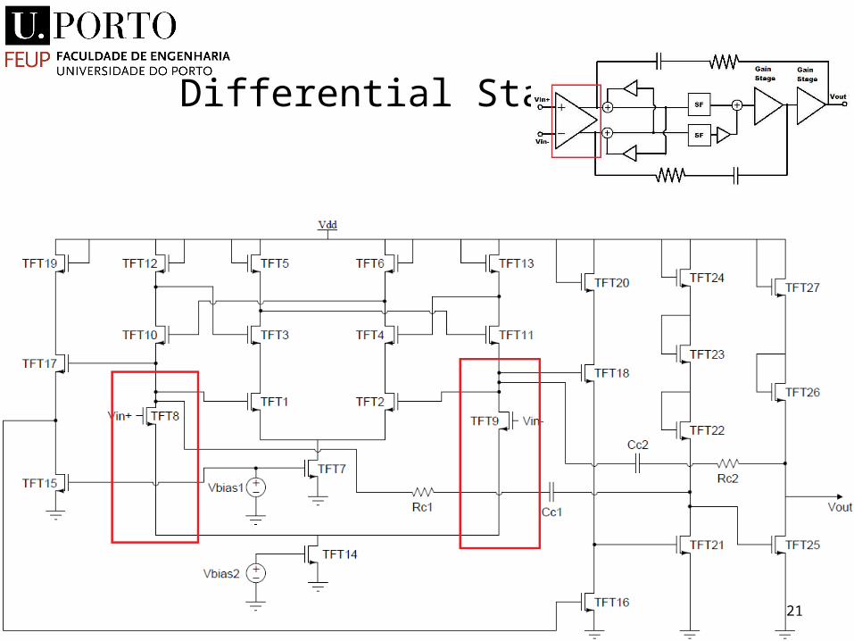
Differential Stage
21

Positive Feedback Stage
22

Source-Follower Stages
23

Common-Source Stages
24

Phase Compensation
-In order to have higher phase margin.
25
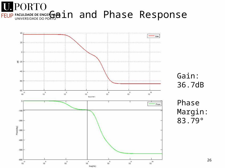
Gain and Phase Response
26
Gain: 36.7dB
Phase Margin: 83.79°

Proposed Amplifier - Layout
27
2383.8 μm
2450 μm

Regulator
28
Voltage levels
Vout = 17.65 VThe voltage variation with the load decreased 80%.

Final Circuit - Layout
2918709.55 μm
14557.1 μm

Fabrication
30DC/DC converter with bootstrapping and 2 boosting stages

Conclusions
• DC/DC converter:– Wide transistors reduce parasitic resistance;– Bootstrapping stage decreases settling time;– 10 converters in parallel reduce the parasitic resistance and
allow more voltage boosting stages, increasing the output voltage level.
• Amplifier:– Good phase margin was achieved;– Voltage gain is enough for the regulation;
• Regulator:– 80% lower fluctuation of the voltage level with load
variations. 31

• Improve the design of the amplifier to increase the gain;
• PWM regulation with duty-cycle variation.
Future Work
32

The End
Thank you!
33