Embed Size (px)
DESCRIPTION
Lab Manual
Citation preview

1
EE2258 LINEAR AND DIGITAL INTEGRATED CIRCUITS LABORATORY
1. Study of Basic Digital IC’s. (Verification of truth table for AND, OR, EXOR, NOT, NOR, NAND, JK FF, RS FF,D FF)
2. Implementation of Boolean Functions, Adder/ Subtractor circuits.
3. a) Code converters, Parity generator and parity checking, Excess-3, 2s
Complement, Binary to Gray code using suitable IC’s .
(b) Encoders and Decoders: Decimal and Implementation of 4-bit shift registers in SISO, SIPO, PISO, PIPO modes using suitable IC’s.
4. Counters: Design and implementation of 4-bit modulo counters as synchronous
and Asynchronous types using FF IC’s and specific counter IC.
5. Shift Registers: Design and implementation of 4-bit shift registers in SISO, SIPO, PISO, PIPO modes using suitable IC’s.
6. Multiplex/ De-multiplex: Study of 4:1; 8:1 multiplexer and Study of 1:4; 1:8
demultiplexer.
7. Timer IC application:Study of NE/SE 555 timer in Astable, Monostable operation.
8. Application of Op-Amp:Slew rate verifications, inverting and non-inverting
amplifier, Adder, comparator, Integrater and Differentiator.
9. Study of Analog to Digital Converter and Digital to Analog Converter: Verification of A/D conversion using dedicated IC’s.
10. Study of VCO and PLL ICs:
i. Voltage to frequency characteristics of NE/ SE 566 IC. ii. Frequency multiplication using NE/SE 565 PLL IC.

2

3
CYCLE-I
1. STUDY OF LOGIC GATES
2. DESIGN OF ADDER AND SUBTRACTOR
3. DESIGN AND IMPLEMENTATION OF CODE CONVERTOR
4. ODD/EVEN PARITY CHECKER/GENERATOR
5. DESIGN AND IMPLEMENTATION OF ENCODER AND DECODER
6. DESIGN AND IMPLEMENTATION OF MULTIPLEXER AND
DEMULTIPLEXER
CYCLE-II
7. STUDY OF FLIP FLOPS
8. DESIGN AND IMPLEMENTATION OF SHIFT REGISTER
9. DESIGN AND IMPLEMENTATION OF 4 BIT SYNCHRONOUS COUNTER
10. DESIGN AND IMPLEMENTATION OF 4 BIT ASYNCHRONOUS
COUNTER
11. DESIGN OF INTEGRATOR AND DIFFERENTIATOR USING OP-AMP 741
12. DESIGN AND IMPLEMENTATION OF MONOSTABLE AND ASTABLE
USING 555 TIMER IC
13. STUDY OF VCO AND PLL

4
AND GATE: SYMBOL: PIN DIAGRAM:
OR GATE:
NOT GATE: SYMBOL: PIN DIAGRAM:
5
EXPT NO. : 01 STUDY OF LOGIC GATES DATE :
AIM:
To study about logic gates and verify their truth tables. APPARATUS REQUIRED:
THEORY: Circuit that takes the logical decision and the process are called logic gates. Each gate has one or more input and only one output.
OR, AND and NOT are basic gates. NAND, NOR and X-OR are known as universal gates. Basic gates form these gates.
AND GATE:
The AND gate performs a logical multiplication commonly known as AND function. The output is high when both the inputs are high. The output is low level when any one of the inputs is low. OR GATE:
The OR gate performs a logical addition commonly known as OR function. The output is high when any one of the inputs is high. The output is low level when both the inputs are low.
SL No. COMPONENT SPECIFICATION QTY
1. AND GATE IC 7408 1
2. OR GATE IC 7432 1
3. NOT GATE IC 7404 1
4. NAND GATE 2 I/P IC 7400 1
5. NOR GATE IC 7402 1
6. X-OR GATE IC 7486 1
7. NAND GATE 3 I/P IC 7410 1
8. IC TRAINER KIT - 1
9. PATCH CORD - 14

6
X-OR GATE : SYMBOL : PIN DIAGRAM :
2-INPUT NAND GATE: SYMBOL: PIN DIAGRAM:
7
NOT GATE: The NOT gate is called an inverter. The output is high when the input is low. The output is low when the input is high. NAND GATE:
The NAND gate is a contraction of AND-NOT. The output is high when both inputs are low and any one of the input is low .The output is low level when both inputs are high.
NOR GATE:
The NOR gate is a contraction of OR-NOT. The output is high when both inputs are low. The output is low when one or both inputs are high.
X-OR GATE:
The output is high when any one of the inputs is high. The output is low when both the inputs are low and both the inputs are high.

8
3-INPUT NAND GATE :
NOR GATE:

9
PROCEDURE:
(i) Connections are given as per circuit diagram. (ii) Logical inputs are given as per circuit diagram. (iii) Observe the output and verify the truth table.
RESULT:
The different logic gates were studied and their truth table was verified using 74XX IC’s.

10
HALF ADDER: TRUTH TABLE: K-Map for SUM: K-Map for CARRY:
SUM = A’B + AB’ CARRY = AB LOGIC DIAGRAM:
FULL ADDER TRUTH TABLE: K-Map for SUM: K-Map for CARRY:
SUM = A’B’C + A’BC’ + ABC’ + ABC CARRY = AB + BC + AC
LOGIC DIAGRAM: FULL ADDER USING TWO HALF ADDER:
A B CARRY SUM 0 0 1 1
0 1 0 1
0 0 0 1
0 1 1 0
A B C CARRY SUM 0 0 0 0 1 1 1 1
0 0 1 1 0 0 1 1
0 1 0 1 0 1 0 1
0 0 0 1 0 1 1 1
0 1 1 0 1 0 0 1

11
EXPT NO. : 02 DESIGN OF ADDER AND SUBTRACTOR
DATE : AIM:
To design and construct half adder, full adder, half subtractor and full subtractor circuits and verify the truth table using logic gates.
APPARATUS REQUIRED:
Sl.No. COMPONENT SPECIFICATION QTY. 1. AND GATE IC 7408 1 2. X-OR GATE IC 7486 1 3. NOT GATE IC 7404 1 4. OR GATE IC 7432 1 3. IC TRAINER KIT - 1 4. PATCH CORDS - 23
THEORY:
HALF ADDER: A half adder has two inputs for the two bits to be added and two outputs one from
the sum ‘ S’ and other from the carry ‘ c’ into the higher adder position. Above circuit is called as a carry signal from the addition of the less significant bits sum from the X-OR Gate the carry out from the AND gate.
FULL ADDER:
A full adder is a combinational circuit that forms the arithmetic sum of input; it consists of three inputs and two outputs. A full adder is useful to add three bits at a time but a half adder cannot do so. In full adder sum output will be taken from X-OR Gate, carry output will be taken from OR Gate. HALF SUBTRACTOR:
The half subtractor is constructed using X-OR and AND Gate. The half subtractor has two input and two outputs. The outputs are difference and borrow. The difference can be applied using X-OR Gate, borrow output can be implemented using an AND Gate and an inverter. FULL SUBTRACTOR:
The full subtractor is a combination of X-OR, AND, OR, NOT Gates. In a full subtractor the logic circuit should have three inputs and two outputs. The two half subtractor put together gives a full subtractor .The first half subtractor will be C and A B. The output will be difference output of full subtractor. The expression AB assembles the borrow output of the half subtractor and the second term is the inverted difference output of first X-OR.

12
HALF SUBTRACTOR K-MAP SIMPLIFICATION: TRUTH TABLE: For Difference: For Borrow:
Difference = A’B + AB’ Borrow = A’B
LOGIC DIAGRAM:
FULL SUBTRACTOR: K-MAP SIMPLIFICATION: TRUTH TABLE: For Difference:
Difference = A’B’C + A’BC’ + AB’C’ + ABC For Borrow:
LOGIC DIAGRAM: Borrow = A’B + BC + A’C FULL SUBTRACTOR USING TWO HALF SUBTRACTOR:
A B BORROW DIFFERENCE 0 0 1 1
0 1 0 1
0 1 0 0
0 1 1 0
A B C BORROW DIFFERENCE 0 0 0 0 1 1 1 1
0 0 1 1 0 0 1 1
0 1 0 1 0 1 0 1
0 1 1 1 0 0 0 1
0 1 1 0 1 0 0 1

13
PROCEEDURE:
(i) Connections are given as per circuit diagram. (ii) Logical inputs are given as per circuit diagram. (iii) Observe the output and verify the truth table.
RESULT: The Adder and subtractor circuits were constructed and their truth table was
verified.

14
BINARY TO GRAY CODE CONVERTOR TRUTH TABLE: K-Map for G3: K-Map for G2:
G3 = B3 G2=B3+ B2
K-Map for G1: K-Map for G0:
LOGIC DIAGRAM:
B3 B2 B1 B0 G3 G2 G1 G0 0 0 0 0 0 0 0 0 1 1 1 1 1 1 1 1
0 0 0 0 1 1 1 1 0 0 0 0 1 1 1 1
0 0 1 1 0 0 1 1 0 0 1 1 0 0 1 1
0 1 0 1 0 1 0 1 0 1 0 1 0 1 0 1
0 0 0 0 0 0 0 0 1 1 1 1 1 1 1 1
0 0 0 0 1 1 1 1 1 1 1 1 0 0 0 0
0 0 1 1 1 1 0 0 0 0 1 1 1 1 0 0
0 1 1 0 0 1 1 0 0 1 1 0 0 1 1 0

15
EXPT NO. :03 DESIGN AND IMPLEMENTATION OF CODE CONVERTOR
DATE : AIM:
To design and implement 4-bit (i) Binary to gray code converter (ii) Gray to binary code converter (iii) BCD to excess-3 code converter (iv) Excess-3 to BCD code converter
APPARATUS REQUIRED:
Sl.No. COMPONENT SPECIFICATION QTY. 1. X-OR GATE IC 7486 1 2. AND GATE IC 7408 1 3. OR GATE IC 7432 1 4. NOT GATE IC 7404 1 5. IC TRAINER KIT - 1 6. PATCH CORDS - 35
THEORY:
The availability of large variety of codes for the same discrete elements of information results in the use of different codes by different systems. A conversion circuit must be inserted between the two systems if each uses different codes for same information. Thus, code converter is a circuit that makes the two systems compatible even though each uses different binary code.
The bit combination assigned to binary code to gray code. Since each code uses four bits to represent a decimal digit. There are four inputs and four outputs. Gray code is a non-weighted code.
The input variable are designated as B3, B2, B1, B0 and the output variables are designated as C3, C2, C1, Co. from the truth table, combinational circuit is designed. The Boolean functions are obtained from K-Map for each output variable.
A code converter is a circuit that makes the two systems compatible even though each uses a different binary code. To convert from binary code to Excess-3 code, the input lines must supply the bit combination of elements as specified by code and the output lines generate the corresponding bit combination of code. Each one of the four maps represents one of the four outputs of the circuit as a function of the four input variables.
A two-level logic diagram may be obtained directly from the Boolean expressions derived by the maps. These are various other possibilities for a logic diagram that implements this circuit. Now the OR gate whose output is C+D has been used to implement partially each of three outputs.

16
GRAY CODE TO BINARY CONVERTOR TRUTH TABLE: K-Map for B3: K-Map for B2:
B3 = G3
K-Map for B1: K-Map for B0:
LOGIC DIAGRAM:
G3 G2 G1 G0 B3 B2 B1 B0 0 0 0 0 0 0 0 0 1 1 1 1 1 1 1 1
0 0 0 0 1 1 1 1 1 1 1 1 0 0 0 0
0 0 1 1 1 1 0 0 0 0 1 1 1 1 0 0
0 1 1 0 0 1 1 0 0 1 1 0 0 1 1 0
0 0 0 0 0 0 0 0 1 1 1 1 1 1 1 1
0 0 0 0 1 1 1 1 0 0 0 0 1 1 1 1
0 0 1 1 0 0 1 1 0 0 1 1 0 0 1 1
0 1 0 1 0 1 0 1 0 1 0 1 0 1 0 1

17
PROCEDURE:
(i) Connections were given as per circuit diagram. (ii) Logical inputs were given as per truth table (iii) Observe the logical output and verify with the truth tables.

18
BCD TO EXCESS-3 CONVERTOR TRUTH TABLE: K-Map for E3: K-Map for E2:
E3 = B3 + B2 (B0 + B1) K-Map for E1: K-Map for E0:
LOGIC DIAGRAM:
B3 B2 B1 B0 E3 E2 E1 E0 0 0 0 0 0 0 0 0 1 1
0 0 0 0 1 1 1 1 0 0
0 0 1 1 0 0 1 1 0 0
0 1 0 1 0 1 0 1 0 1
0 0 0 0 0 1 1 1 1 1
0 1 1 1 1 0 0 0 0 1
1 0 0 1 1 0 0 1 1 0
1 0 1 0 1 0 1 0 1 0

19

20
EXCESS-3 TO BCD CONVERTOR TRUTH TABLE: K-Map for A: K-Map for B:
A = X1 X2 + X3 X4 X1 K-Map for C: K-Map for D:
LOGIC DIAGRAM:
X1 X2 X3 X4 A B C D 0 0 0 0 0 1 1 1 1 1
0 1 1 1 1 0 0 0 0 1
1 0 0 1 1 0 0 1 1 0
1 0 1 0 1 0 1 0 1 0
0 0 0 0 0 0 0 0 1 1
0 0 0 0 1 1 1 1 0 0
0 0 1 1 0 0 1 1 0 0
0 1 0 1 0 1 0 1 0 1

21
RESULT: The 4 bit code converters were designed and their truth table was verified.

22
Logic diagrams: Odd parity checker:
A
B
C
DODD PARITY
74LS86A
10
98
74LS86A
4
5674LS86A
1
23
Even parity checker:
AB
C
DODD PARITY EVEN PARITY
74LS86A
10
98
74LS86A
4
5674LS86A
1
23
74LS04
1 2
Odd parity generator:
A
AB
B
C
C
D
D
PARITY BIT
74LS86A
10
98
74LS86A
4
56
74LS86A
1
23
74LS04
1 2
Even parity generator:
AB
BA
C
C
D
D
PARITY BIT74LS86A
1
23
74LS86A
4
56
74LS86A
10
98

23
EXPT NO. : 3(b) PARITY CHECKER AND GENERATORS DATE : AIM:
To implement the odd and even parity checkers using the logic gates and also to generate the odd parity and even parity numbers using the generators. APPARATUS REQUIRED:
Theory:
Parity checking is used for error detection in data transmission. Odd parity checkers: It counts the number of 1’s in the given input and produces a 1 in the output when the number of 1’s is odd. Even parity checker: It counts the number of 1’s in the given input and produces a 1 in the output when the number of 1’s is even. Odd parity generators: It generates an odd parity number. The odd parity checker circuit is used with the inverted output and also the input bits. So when the input is a 4-bit number then the output of the generator circuit will have 5 bits which is an odd parity number. Even parity generator: It generates an even parity number. The even parity checker circuit is used with the inverted output and also the input bits. So when the input is a 4-bit number then the output of the generator circuit will have 5 bits which is an even parity number. Procedure:
The circuit is implemented using logic gates.
The inputs are given as per the truth table.
The corresponding outputs are noted.
The theoretical and practical values were verified.
Sl.No Component Type Quantity 1 Trainer Kit - 1 5 EX-OR IC7486 1 5 NOT gate IC 7404 1 6 Connecting wires - Required

24
TRUTH TABLE:
Input Checker output Generator output A B C D odd even odd even 0 0 0 0 0 1 00001 00000 0 0 0 1 1 0 00010 00011 0 0 1 0 1 0 00100 00101 0 0 1 1 0 1 00111 00110 0 1 0 0 1 0 01000 01001 0 1 0 1 0 1 01011 01010 0 1 1 0 0 1 01101 01100 0 1 1 1 1 0 01110 01111 1 0 0 0 1 0 10000 10001 1 0 0 1 0 1 10011 10010 1 0 1 0 0 1 10101 10100 1 0 1 1 1 0 10110 10111 1 1 0 0 0 1 11001 11000 1 1 0 1 1 0 11010 11011 1 1 1 0 1 0 11100 11101 1 1 1 1 0 1 11111 11110

25
RESULT : The odd and even parity checkers are implemented using the logic gates and the odd parity and even parity numbers are generated using the corresponding generators.

26
PIN DIAGRAM FOR IC 7445:
BCD TO DECIMAL DECODER:
PIN DIAGRAM FOR IC 74147:
27
EXPT NO. :4 DESIGN AND IMPLEMENTATION OF ENCODER AND DECODER
DATE :
AIM:
To design and implement encoder and decoder using logic gates and study of IC
7445 and IC 74147.
APPARATUS REQUIRED:
Sl.No. COMPONENT SPECIFICATION QTY.
1. 3 I/P NAND GATE IC 7410 2
2. OR GATE IC 7432 3
3. NOT GATE IC 7404 1
2. IC TRAINER KIT - 1
3. PATCH CORDS - 27
THEORY:
ENCODER:
An encoder is a digital circuit that perform inverse operation of a decoder. An
encoder has 2n input lines and n output lines. In encoder the output lines generates the
binary code corresponding to the input value. In octal to binary encoder it has eight
inputs, one for each octal digit and three output that generate the corresponding binary
code. In encoder it is assumed that only one input has a value of one at any given time
otherwise the circuit is meaningless. It has an ambiguila that when all inputs are zero the
outputs are zero. The zero outputs can also be generated when D0 = 1.
DECODER:
A decoder is a multiple input multiple output logic circuit which converts coded
input into coded output where input and output codes are different. The input code
generally has fewer bits than the output code. Each input code word produces a different
output code word i.e there is one to one mapping can be expressed in truth table. In the
block diagram of decoder circuit the encoded information is present as n input producing
2n possible outputs. 2n output values are from 0 through out 2n – 1.

28
LOGIC DIAGRAM FOR ENCODER:
TRUTH TABLE:
INPUT OUTPUT
Y1 Y2 Y3 Y4 Y5 Y6 Y7 A B C
1 0 0 0 0 0 0 0 0 1
0 1 0 0 0 0 0 0 1 0
0 0 1 0 0 0 0 0 1 1
0 0 0 1 0 0 0 1 0 0
0 0 0 0 1 0 0 1 0 1
0 0 0 0 0 1 0 1 1 0
0 0 0 0 0 0 1 1 1 1

29
PROCEDURE:
(i) Connections are given as per circuit diagram. (ii) Logical inputs are given as per circuit diagram. (iii) Observe the output and verify the truth table.
RESULT: Thus the Encoder and Decoder circuit was designed and the output was verified.
30
MULTIPLEXER: BLOCK DIAGRAM FOR 4:1 MULTIPLEXER:
FUNCTION TABLE:
S1 S0 INPUTS Y
0 0 D0 → D0 S1’ S0’
0 1 D1 → D1 S1’ S0
1 0 D2 → D2 S1 S0’
1 1 D3 → D3 S1 S0
Y = D0 S1’ S0’ + D1 S1’ S0 + D2 S1 S0’ + D3 S1 S0
TRUTH TABLE:
S1 S0 Y = OUTPUT
0 0 D0
0 1 D1
1 0 D2
1 1 D3
31
EXPT NO. :05 DESIGN AND IMPLEMENTATION OF MULTIPLEXER AND
DEMULTIPLEXER DATE : AIM: To design and implement multiplexer and demultiplexer using logic gates and study of IC 74150 and IC 74154. APPARATUS REQUIRED:
Sl.No. COMPONENT SPECIFICATION QTY. 1. 3 I/P AND GATE IC 7411 2 2. OR GATE IC 7432 1 3. NOT GATE IC 7404 1 2. IC TRAINER KIT - 1 3. PATCH CORDS - 32
THEORY: MULTIPLEXER:
Multiplexer means transmitting a large number of information units over a smaller number of channels or lines. A digital multiplexer is a combinational circuit that selects binary information from one of many input lines and directs it to a single output line. The selection of a particular input line is controlled by a set of selection lines. Normally there are 2n input line and n selection lines whose bit combination determine which input is selected.
DEMULTIPLEXER: The function of Demultiplexer is in contrast to multiplexer function. It takes information from one line and distributes it to a given number of output lines. For this reason, the demultiplexer is also known as a data distributor. Decoder can also be used as demultiplexer.
In the 1: 4 demultiplexer circuit, the data input line goes to all of the AND gates. The data select lines enable only one gate at a time and the data on the data input line will pass through the selected gate to the associated data output line.

32
CIRCUIT DIAGRAM FOR MULTIPLEXER:
DEMULTIPLEXER: BLOCK DIAGRAM FOR 1:4 DEMULTIPLEXER:
FUNCTION TABLE:
S1 S0 INPUT 0 0 X → D0 = X S1’ S0’ 0 1 X → D1 = X S1’ S0 1 0 X → D2 = X S1 S0’ 1 1 X → D3 = X S1 S0
Y = X S1’ S0’ + X S1’ S0 + X S1 S0’ + X S1 S0

33
PROCEDURE:
(i) Connections are given as per circuit diagram. (ii) Logical inputs are given as per circuit diagram. (iii) Observe the output and verify the truth table.

34
TRUTH TABLE:
INPUT OUTPUT S1 S0 I/P D0 D1 D2 D3 0 0 0 0 0 0 0 0 0 1 1 0 0 0 0 1 0 0 0 0 0 0 1 1 0 1 0 0 1 0 0 0 0 0 0 1 0 1 0 0 1 0 1 1 0 0 0 0 0 1 1 1 0 0 0 1
LOGIC DIAGRAM FOR DEMULTIPLEXER:

35
RESULT : The multiplexer and demultiplexer circuits are constructed and their truth table was verified.

36
PIN DIAGRAM:
SERIAL IN SERIAL OUT: LOGIC DIAGRAM:
TRUTH TABLE:
CLK
Serial in Serial out
1 1 0
2 0 0
3 0 0
4 1 1
5 X 0
6 X 0
7 X 1

37
EXPT NO. :6 DESIGN AND IMPLEMENTATION OF SHIFT REGISTER DATE :
AIM:
To design and implement (i) Serial in serial out (ii) Serial in parallel out (iii) Parallel in serial out (iv) Parallel in parallel out
APPARATUS REQUIRED:
Sl.No. COMPONENT SPECIFICATION QTY. 1. D FLIP FLOP IC 7474 2 2. OR GATE IC 7432 1 3. IC TRAINER KIT - 1 4. PATCH CORDS - 35
THEORY:
A register is capable of shifting its binary information in one or both directions is known as shift register. The logical configuration of shift register consist of a D-Flip flop cascaded with output of one flip flop connected to input of next flip flop. All flip flops receive common clock pulses which causes the shift in the output of the flip flop. The simplest possible shift register is one that uses only flip flop. The output of a given flip flop is connected to the input of next flip flop of the register. Each clock pulse shifts the content of register one bit position to right. PROCEDURE:
(i) Connections are given as per circuit diagram. (ii) Logical inputs are given as per circuit diagram. (iii) Observe the output and verify the truth table.

38
SERIAL IN PARALLEL OUT: LOGIC DIAGRAM:
TRUTH TABLE:
CLK
DATA
OUTPUT
QA QB QC QD 1 1 1 0 0 0
2 0 0 1 0 0
3 0 0 0 1 1
4 1 1 0 0 1
PARALLEL IN SERIAL OUT: LOGIC DIAGRAM:
TRUTH TABLE:
CLK Q3 Q2 Q1 Q0 O/P 0 1 0 0 1 1 1 0 0 0 0 0 2 0 0 0 0 0 3 0 0 0 0 1

39
40
PARALLEL IN PARALLEL OUT: LOGIC DIAGRAM:
TRUTH TABLE: CLK
DATA INPUT OUTPUT DA DB DC DD QA QB QC QD
1 1 0 0 1 1 0 0 1 2 1 0 1 0 1 0 1 0

41
RESULT : Thus the Shift Registers was designed and their output was verified.

42
PIN DIAGRAM :
4-bit Synchronous Counter Waveform Timing Diagram.

43
EXPT NO. :7(a) DESIGN AND IMPLEMENTATION OF 4 BIT DATE : SYNCHRONOUS COUNTER
AIM: To design and realize a 4-bit synschronous counter APPARATUS REQUIRED: IC 7408, IC 7476, IC 7400, IC 7432 etc.
Procedure:
1. Connections are made as per circuit diagram.
2. Clock pulses are applied one by one at the clock I/P and the O/P is
observed at QA, QB & QC for IC 7476.
3. Verify the Truth table .
THEORY:
It can be seen that the external clock pulses (pulses to be counted) are fed directly to each
J-K flip-flop in the counter chain and that both the J and K inputs are all tied together in
toggle mode, but only in the first flip-flop, flip-flop A (LSB) are they connected HIGH,
logic "1" allowing the flip-flop to toggle on every clock pulse. Then the synchronous
counter follows a predetermined sequence of states in response to the common clock
signal, advancing one state for each pulse.
The J and K inputs of flip-flop B are connected to the output "Q" of flip-flop A, but the J
and K inputs of flip-flops C and D are driven from AND gates which are also supplied
with signals from the input and output of the previous stage. If we enable each J-K flip-
flop to toggle based on whether or not all preceding flip-flop outputs (Q) are "HIGH" we
can obtain the same counting sequence as with the asynchronous circuit but without the
ripple effect, since each flip-flop in this circuit will be clocked at exactly the same time.
As there is no propagation delay in synchronous counters because all the counter stages
are triggered in parallel the maximum operating frequency of this type of counter is much
higher than that of a similar asynchronous counter. Because this 4-bit synchronous
counter counts sequentially on every clock pulse the resulting outputs count upwards
from 0 ( "0000" ) to 15 ( "1111" ). Therefore, this type of counter is also known as a 4-bit
Synchronous Up Counter.

44
Binary 4-bit Synchronous Counter
Truth Table for JK flip-flop:
TRUTH TABLE
J K Qn+1
0 0 1 1
0 1 0 1
Qn
0 1
Qn
COUNT OUTPUTS
QD QC QB QA
0 0 0 0 0
1 0 0 0 1
2 0 0 1 0
3 0 0 1 1
4 0 1 0 0
5 0 1 0 1
6 0 1 1 0
7 0 1 1 1
8 1 0 0 0
9 1 0 0 1
10 1 0 1 0
11 1 0 1 1
12 1 1 0 0
13 1 1 0 1
14 1 1 1 0
15 1 1 1 1

45
RESULT : Thus the 4-bit synchronous counter was designed and its truth table was verified.
46
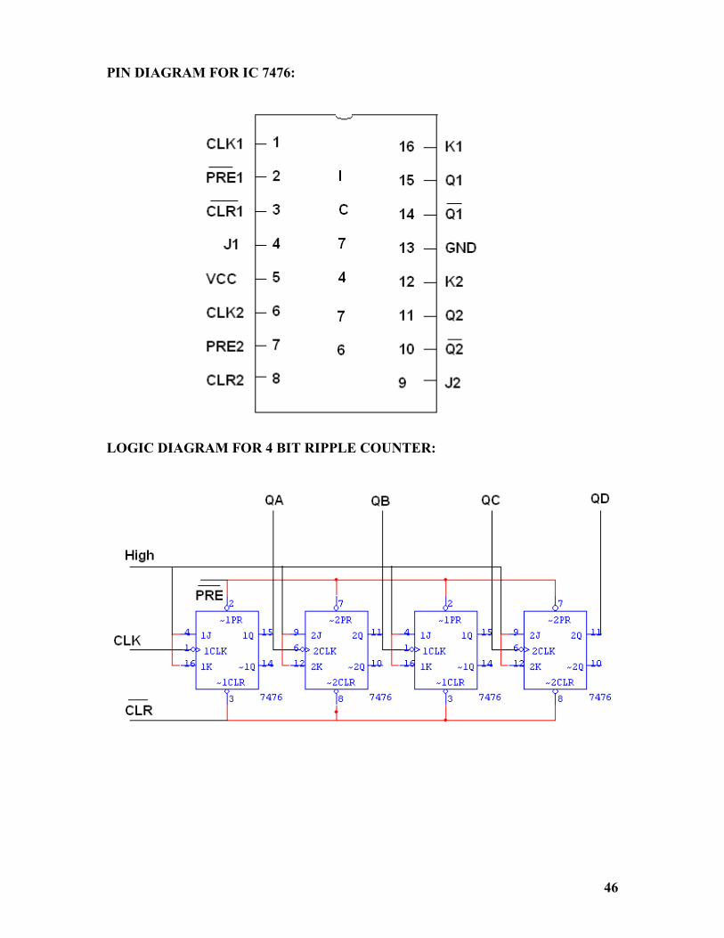
PIN DIAGRAM FOR IC 7476:
LOGIC DIAGRAM FOR 4 BIT RIPPLE COUNTER:

47
EXPT NO. :7b) DESIGN AND IMPLEMENTATION OF 4 BIT DATE : ASYNCHRONOUS COUNTER
AIM: To design and realize a 4-bit Asynschronous counter APPARATUS REQUIRED:
Sl.No. COMPONENT SPECIFICATION QTY.
1. JK FLIP FLOP IC 7476 2
2. NAND GATE IC 7400 1
3. IC TRAINER KIT - 1
4. PATCH CORDS - 30
THEORY:
A counter is a register capable of counting number of clock pulse arriving at its clock
input. Counter represents the number of clock pulses arrived. A specified sequence of states
appears as counter output. This is the main difference between a register and a counter. There are
two types of counter, synchronous and asynchronous. In synchronous common clock is given to
all flip flop and in asynchronous first flip flop is clocked by external pulse and then each
successive flip flop is clocked by Q or Q output of previous stage. A soon the clock of second
stage is triggered by output of first stage. Because of inherent propagation delay time all flip flops
are not activated at same time which results in asynchronous operation. A simple implementation
of a 4-bit counter is shown in Figure 1, which consists of 4 stages of cascaded J-K flip-flops. This
is a binary counter, since the output is in binary system format, i.e., only two digits are used to
represent the count, i.e., '1' and '0'. With only 4 bits, it can only count up to '1111', or decimal
number 15. The J and K inputs of all the flip-flops are tied to '1', so that they will toggle between
states every time they are clocked. Also, the output of each flip-flop in the counter is used to
clock the next flip-flop. As a result, the succeeding flip-flop toggles between '1' and '0' at only
half the frequency as the flip-flop before it.
The last flip-flop will only toggle after the first flip-flop has already toggled 8 times.
This type of binary counter is known as a 'serial', 'ripple', or 'asynchronous' counter. The name
'asynchronous' comes from the fact that this counter's flip-flops are not being clocked at the same
time.

48
TRUTH TABLE:
CLK QA QB QC QD
0 0 0 0 0
1 1 0 0 0
2 0 1 0 0
3 1 1 0 0
4 0 0 1 0
5 1 0 1 0
6 0 1 1 0
7 1 1 1 0
8 0 0 0 1
9 1 0 0 1
10 0 1 0 1
11 1 1 0 1
12 0 0 1 1
13 1 0 1 1
14 0 1 1 1
15 1 1 1 1

49
A 4-bit counter, which has 16 unique states that it can count through, is also called a
modulo-16 counter, or mod-16 counter. By definition, a modulo-k or base-k counter is one that
returns to its initial state after k cycles of the input waveform. A counter that has N flip-flops is a
modulo 2N counter.
An asynchronous counter has a serious drawback - its speed is limited by
the cumulative propagation times of the cascaded flip-flops. A counter that has N flip-
flops, each of which has a propagation time t, must therefore wait for a duration equal to
N x t before it can undergo another transition clocking.
RESULT : Thus the 4-bit asynchronous counter was designed and its truth table was verified.

50
LOGIC SYMBOL:
CIRCUIT DIAGRAM:
CHARACTERISTIC TABLE:
CLOCK
PULSE
INPUT PRESENT
STATE (Q)
NEXT
STATE(Q+1)
STATUS
S R
1 0 0 0 0
2 0 0 1 1
3 0 1 0 0
4 0 1 1 0
5 1 0 0 1
6 1 0 1 1
7 1 1 0 X
8 1 1 1 X

51
EXPT NO. :8 STUDY OF FLIPFLOPS DATE :
AIM:
To verify the characteristic table of RS, D, JK, and T Flip flops .
APPARATUS REQUIRED:
S.No Name of the Apparatus Range Quantity
1. Digital IC trainer kit 1
2. NOR gate IC 7402
3. NOT gate IC 7404
4. AND gate ( three input ) IC 7411
5. NAND gate IC 7400
6. Connecting wires As required
THEORY:
A Flip Flop is a sequential device that samples its input signals and changes its
output states only at times determined by clocking signal. Flip Flops may vary in the
number of inputs they possess and the manner in which the inputs affect the binary states.
RS FLIP FLOP:
The clocked RS flip flop consists of NAND gates and the output changes its
state with respect to the input on application of clock pulse. When the clock pulse is high
the S and R inputs reach the second level NAND gates in their complementary form.
The Flip Flop is reset when the R input high and S input is low. The Flip Flop is set
when the S input is high and R input is low. When both the inputs are high the output is
in an indeterminate state.
D FLIP FLOP:
To eliminate the undesirable condition of indeterminate state in the SR Flip
Flop when both inputs are high at the same time, in the D Flip Flop the inputs are never
made equal at the same time. This is obtained by making the two inputs complement of
each other.
JK FLIP FLOP:
The indeterminate state in the SR Flip-Flop is defined in the JK Flip Flop. JK
inputs behave like S and R inputs to set and reset the Flip Flop. The output Q is ANDed
with K input and the clock pulse, similarly the output Q’ is ANDed with J input and the
Clock pulse. When the clock pulse is zero both the AND gates are disabled and the Q
and Q’ output retain their previous values. When the clock pulse is high, the J and K
inputs reach the NOR gates. When both the inputs are high the output toggles
continuously. This is called Race around condition and this must be avoided.

52
D FLIP FLOP
LOGIC SYMBOL:
CIRCUIT DIAGRAM:
CHARACTERISTIC TABLE:
CLOCK
PULSE
INPUT
D
PRESENT
STATE (Q)
NEXT
STATE(Q+1)
STATUS
1 0 0 0
2 0 1 0
3 1 0 1
4 1 1 1

53

54
JK FLIP FLOP
LOGIC SYMBOL:
CIRCUIT DIAGRAM:
CHARACTERISTIC TABLE:
CLOCK
PULSE
INPUT PRESENT
STATE (Q)
NEXT
STATE(Q+1)
STATUS
J K
1 0 0 0 0
2 0 0 1 1
3 0 1 0 0
4 0 1 1 0
5 1 0 0 1
6 1 0 1 1
7 1 1 0 1
8 1 1 1 0

55
56
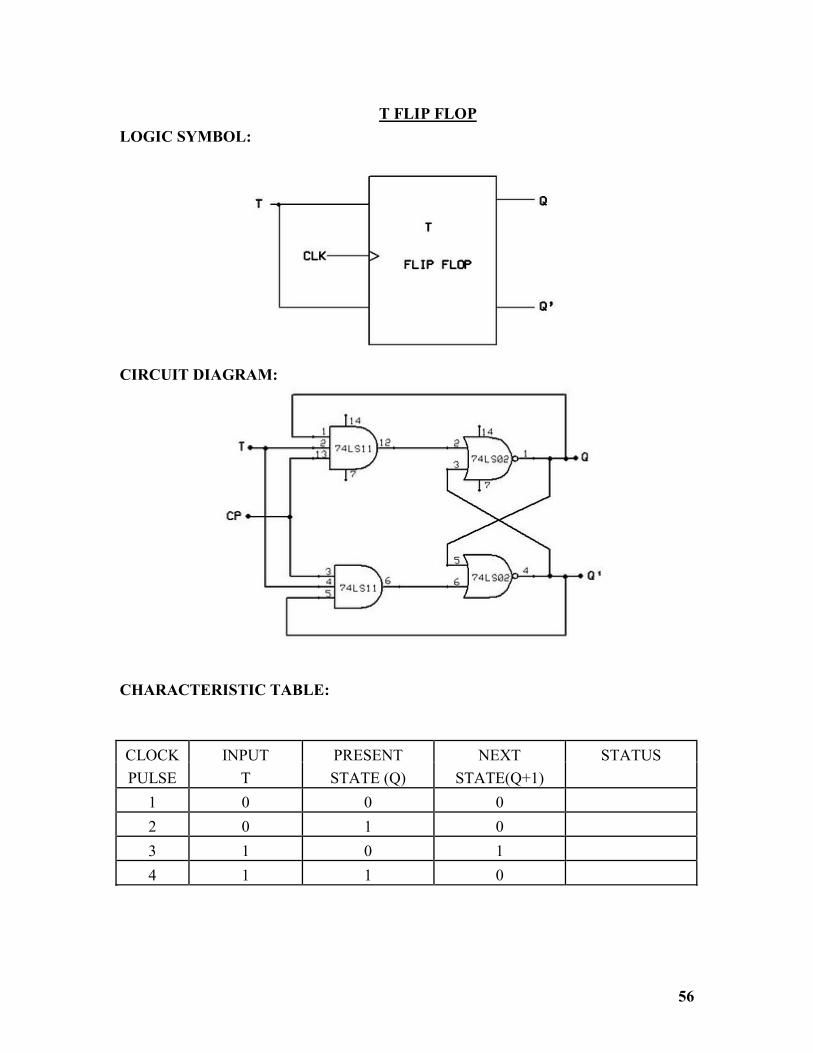
T FLIP FLOP
LOGIC SYMBOL:
CIRCUIT DIAGRAM:
CHARACTERISTIC TABLE:
CLOCK
PULSE
INPUT
T
PRESENT
STATE (Q)
NEXT
STATE(Q+1)
STATUS
1 0 0 0
2 0 1 0
3 1 0 1
4 1 1 0

57
PROCEDURE:
1. Connections are given as per the circuit diagrams.
2. For all the ICs 7th pin is grounded and 14th pin is given +5 V supply.
3. Apply the inputs and observe the status of all the flip flops.
RESULT:
The Characteristic tables of RS, D, JK, T flip flops were verified.

58
PIN DIAGRAM OF 741 :
INTEGRATOR :
FORMULA USED :

59
EXPT NO. :9 INTEGRATOR AND DIFFERENTIATOR DATE : AIM:
To design a differentiator and Integrator circuit using op-amps IC 741. APPARATUS REQUIRED: 1.IC 741 2.Resistors 3.Capacitors 4.AFO 5.CRO 6.Bread board 7.Connecting wires OPREATIONAL AMPLIFIER :
An operational amplifier, often referred as an op-amp, is a very high gain
performance amplifier designed to amplify ac and dc voltage voltages used to perform
arithmetic operations (addition, subtraction, multiplication) with signals. In fact, op amps
can also be used to integrate (calculate the areas under) and differentiate (calculate the
slopes of) signals.
A differentiator circuit produces a constant output voltage for a steadily changing input
voltage. An integrator circuit produces a steadily changing output voltage for a constant
input voltage. Both types of devices are easily constructed, using reactive components
(usually capacitors rather than inductors) in the feedback part of the circuit.
In the integrator circuit we have replaced the feedback resistor with a capacitor.
Therefore, any feedback current must be based on a change in output voltage. As
feedback current flows, the capacitor will gain an electric charge, which will change
according to the cumulative effects of the output signal.If the input voltage is zero, no
input current will flow. Therefore no feedback current can flow and the output voltage
will remain constant. If the input voltage is non-zero, the basic equation for the output
voltage becomes Vout = -Vin/RC + K, where R is the input resistance in ohms, C is the
feedback capacitance in farads, and K is a fixed constant representing the accumulated
voltage from the past.If the input voltage is constantly changing, the output voltage at any
instant will be the integral of all past input voltage values. For example, a bipolar sine
wave input will actually produce another sine wave as its output, at a phase angle of 90°
from the input sine wave. Technically, the output will be an inverted cosine wave.

60
DIFFERENTIATOR :
GAIN CALCULATION:
An operational amplifier purpose is to amplify a weak signal and this is called the GAIN.
INVERTING AMPLIFIER GAIN (AV) = -R2 / R1 Example : if R2 is 100 kilo-ohm and R1 is 10 kilo-ohm the gain would be : -100 / 10 = -10 (Gain AV) If the input voltage is 0.5v the output voltage would be : 0.5v X -10 = -5v
NON-INVERTING AMPLIFIER GAIN (AV) = 1+(R2 / R1) Example : if R2 is 1000 kilo-ohm and R1 is 100 kilo-ohm the gain would be : 1+ (1000/100) = 1 + 10 OR GAIN (AV) = 11 If the input voltage is 0.5v the output voltage would be : 0.5 X 11 = 5.5v

61
In the differentiator circuit, Since the input circuit element is a capacitor, this circuit will
only experience input current in response to changes in input voltage the faster and larger
the change in input voltage, the greater the input current, therefore the greater the output
voltage in response.
Since the output voltage will reflect the rate of change of the input, this circuit will
indeed perform differentiation. The "d/dt" notation indicates differentiation with respect
to time. If you're not familiar with differential calculus, don't worry about it here; you
won't need it for these pages.
The op amp differentiator is not used in any analog computer application, and indeed not
generally. The basic reason for this is that high-frequency noise signals will not be
suppressed by this circuit; rather they will be amplified far beyond the amplification of
the desired signal.
The formula for determining voltage output for the differentiator is as follows:
In some applications, it may be possible to add a series input resistor, as shown in the
schematic diagram to the right. This limits the high frequency gain of the circuit to the
ratio Rf/Rin. The low frequency gain is still set by Rf and C, as before. The cutoff
frequency, where these two effects meet, is determined by Rin and C, according to the
expression: fco = 1/2 RinC.Higher-frequency signals are still amplified more than low-
frequency signals, so any noise present in the circuit will still be amplified more than the
desired signal. If an application can suppress such noise and doesn't require higher-
frequency components, this modified circuit may serve the need. In other cases, if
differentiation is absolutely required, a passive RC circuit is generally used instead, and
the inevitable signal losses compensated later.

62

63
Linear Integrating and Non-Integrating Amplifiers:
Op-amps can be used in an enormous variety of different types of circuit but one
of the most common is within amplifier circuits themselves. Here they enable high
performance circuits to be made with a minimum number of components. There are two
common formats for amplifiers using op-amp based circuits:
Non-inverting amplifier circuit: - here the output is in the same sense as the
input signal, i.e. when the input voltage goes positive, so does the output.
In this circuit, the input signal is effectively used as the reference voltage at the
"+" input to the differential amplifier, while the "-" input is indirectly referenced
to ground. In order to keep the two input voltages to the amplifier the same, the
amplifier must set Vout to whatever voltage is required to make the feedback
voltage to the "-" input match the input voltage to the "+" input.
Since Rf and Rin form a voltage divider, the feedback voltage will be
VoutRin/(Rf + Rin). The gain of this circuit, then, calculated as Vout/Vin, is
(Rf + Rin)/Rin, or (Rf/Rin) + 1. Resistor Rz has no effect on the gain of the circuit.
However, to balance out variations caused by the small input current to the
amplifier, Rz should be made equal to the parallel combination of Rf and Rin.
Inverting amplifier circuit: - here the output is an inverted version (upside
down) of the signal that enters the circuit, i.e. when the input voltage goes more
positive, the output goes more negative.
Procedure: 1.Put the op amp in the breadboard and connect +Vcc and -Vcc to the
chip. Set the magnitude of Vcc to 12 volts (you will have to check this with a voltmeter).
Connect the rest of the circuit with R1=10kΩ and Rf=30kΩ. You should verify that the
resistor values are correct by reading them off the resistor (they are sometimes in the
wrong drawer). 2.Derive an expression for vout/vin for the inverting amplifier, in terms of
R1 and Rf. 3.Now drive the inverting amplifier with a 1 kHz sine wave, that is 2
volts peak-to-peak. Hook up the oscilloscope so you can see both vin and vout.
RESULT: Thus the integrator and differentiator using opamp 741 was designed and verified.

64
ASTABLE MULTIVIBRATOR :
R1
1k
R2
1k
C1
1n C2
1n
21
8 4
3
6
7
5
555
v cc
o/p
DESIGN: Astable multivibrator: For 50% duty cycle: Tc= 0.69(Ra+Rb)*C Td= 0.69Rb* C T = Tc+Td T = 0.69(Ra+2Rb)*C f = 1/T = 1.45/(Ra+2Rb)*C % Duty cycle D = Td/T*100 D = Ra/(Ra+2Rb)*C Let Tc = Td = 0.05 msec Choose C = 10nf 0.05*10-3 = 0.69(Ra+Rb)*10n Therefore Ra+Rb = 7.215k Choose Ra=470Ω Rb=6.8kΩ Tabulation: Astable Multivibrator: Theoritical Practical
ON time
OFF time
% Duty cycle
Frequency

65
EXPT NO. :10 MULTIVIBRATOR USING 555 TIMER DATE : AIM: To design and construct the astable and mono stable multivibrator using 555 timer. Draw the waveform. APPARATUS REQUIRED:
S.No Apparatus Range Quantity
1.
2.
3. 4. 5. 6. 7. 8.
Resistor Capacitor Timer IC RPS AFO CRO Bread board Connecting wires
6.8kΩ,10kΩ
470Ω 470pF,
.1nF,1μF NE555
- -
(0-30)v - -
1,2 1
1,1 1 1 1 1 1 1 -
Pin 1. − Ground, The ground pin connects the 555 timer to the negative (0v) supply.
Pin 2. − Trigger, The negative input to comparator No 1. A negative pulse on this pin
"sets" the internal Flip-flop when the voltage drops below 1/3Vcc causing the output to
switch from a "LOW" to a "HIGH" state.
Pin 3. − Output, The output pin can drive any TTL circuit and is capable of sourcing or
sinking up to 200mA of current at an output voltage equal to approximately Vcc - 1.5V
so small speakers, LEDs or motors can be connected directly to the output.
Pin 4. − Reset, This pin is used to "reset" the internal Flip-flop controlling the state of
the output, pin 3. This is an active-low input and is generally connected to a logic "1"
level when not used to prevent any unwanted resetting of the output.
Pin 5. − Control Voltage, This pin controls the timing of the by overriding the 2/3Vcc
level of the voltage divider network. By applying a voltage to this pin the width of the
output signal can be varied independently of the RC timing network. When not used it is
connected to ground via a 10nF capacitor to eliminate any noise.
Pin 6. − Threshold, The negative input to comparator No 2. This pin is used to reset the
Flip-flop when the voltage applied to it exceeds 2/3Vcc causing the output to switch from
HIGH" to "LOW" state. This pin connects directly to the RC timing circuit.

66
MONOSTABLE MULTIVIBRATOR :
Monostable Multivibrator: Tp = 1.1 RC For Tp = 0.1ms Choose C= 0.01μF To Find R R =Tp/1.1C=10KΩ
TABULATION :
Monostable Multivibrator: Theoritical Practical
ON time
OFF time
% Duty cycle
Frequency
R2
1k
C1
1n
C2
1n
2
1
4
3
7
5
8
6
vcc
555
o/p
C3
1n
R3
1k
D1
DIODE
I/P

67
Pin 7. − Discharge, The discharge pin is connected directly to the Collector of an
internal NPN transistor which is used to "discharge" the timing capacitor to ground when
the output at pin 3 switches "LOW".
Pin 8. − Supply +Vcc, This is the power supply pin and for general purpose TTL 555
timers is between 4.5V and 15V.
Theory: Astable multivibrator: An astable multivibrator is a wave-generating circuit in which neither of the output
levels is stable. The output keeps on switching between the two unstable states and is a
periodic, rectangular waveform. The circuit is therefore known as an ‘astable
multivibrator’. Also, no external trigger is required to change the state of the output,
hence it is also called ‘free-running multivibrator’. The time for which the output remains
in one particular state is determined by the two resistors and a capacitor externally
connected to the 555 timer. In the 555 Oscillator above, pin 2 and pin 6 are connected
together allowing the circuit to re-trigger itself on each and every cycle allowing it to
operate as a free running oscillator. During each cycle capacitor, C charges up through
both timing resistors, R1 and R2 but discharges itself only through resistor, R2 as the
other side of R2 is connected to the Discharge terminal, pin 7. Then the capacitor charges
up to 2/3Vcc (the upper comparator limit) which is determined by the 0.693(R1+R2)C
combination and discharges itself down to 1/3Vcc (the lower comparator limit)
determined by the 0.693(R2.C) combination. This results in an output waveform whose
voltage level is approximately equal to Vcc - 1.5V and whose output "ON" and "OFF"
time periods are determined by the capacitor and resistors combinations.
Monostable Multivibrator: A monostable multivibrator is a pulse-generating circuit having one stable
and one quasi-stable state. Since there is only one stable state, the circuit is known as
‘monostable multivibrator’. The duration of the output pulse is determined by the RC
network connected externally to the 555 timer. The stable state output is approximately
zero or at logic-low level. An external trigger pulse forces the output to become high or
approximately. After a predetermined length of time, the output automatically switches
back to the stable state and remains low until a trigger pulse is again applied. The cycle
then repeats.

68

69
That is, each time a trigger pulse is applied, the circuit produces a single pulse. Hence, it
is also called ‘one-shot multivibrator’. A monostable multivibrator is a timing circuit that
changes state once triggered, but returns to its original state after a certain time delay. It
got its name from the fact that only one of its output states is stable. It is also known as a
'one-shot'.
Pin 1 is grounded. Trigger input is applied to pin 2. In quiescent
condition of output this input is kept at + VCC. To obtain transition of output from stable
state to quasi-stable state, a negative-going pulse of narrow width (a width smaller than
expected pulse width of output waveform) and amplitude of greater than + 2/3 VCC is
applied to pin 2. Output is taken from pin 3. Pin 4 is usually connected to + VCC to avoid
accidental reset. Pin 5 is grounded through a 0.01 u F capacitor to avoid noise problem.
Pin 6 (threshold) is shorted to pin 7. A resistor RA is connected between pins 6 and 8. At
pins 7 a discharge capacitor is connected while pin 8 is connected to supply VCC.
PROCEDURE: Astable multivibrator: 1.Connections are made as per the circuit diagram.
2.The output waveforms are viewed through CRO.
3.The voltage across the capacitor and that at the output terminal is
measured and the waveforms are drawn.
Monostable multivibrator 1.Connections are made as per the circuit diagram.
2.A low frequency trigger pulse is applied.
3.The output waveforms are viewed through CRO.
. 4.The voltage across the capacitor and that at the output terminal is
measured.
RESULT: Thus the astable and mono stable multivibrator using 555 timer are designed and the waveforms are drawn.

70
BLOCK DIAGRAM OF BASIC PHASE LOCKED LOOP :

71
EXPT NO. :11 STUDY OF VCO AND PLL DATE :
Introduction to PLL or Phase Locked Loops
Phase-locked loop is a feedback loop consisting of a phase detector, a low-pass
filter, amplifier (optional) and a voltage-controlled oscillator (VCO), as illustrated in
figure. It plays the same role in the frequency or phase world as the op-amp does in the
voltage world. The op-amp has two voltage inputs, non-inverting and inverting (normally
used for feedback from the output). Similarly, the PLL has two inputs; the PLL’s
feedback input is normally connected to the circuits’ output. Digital frequencies are
usually applied. The op-amp changes its output voltage to whatever values is necessary to
drive the difference in voltage between its two inputs to zero. The PLL changes its output
phase and frequency to whatever frequency or phase is necessary to make the two input
frequencies and phase track. Placing a voltage divider in the feedback loop of an op-amp
causes the output voltage to be increased by the amount of the feedback voltage division
(amplification). Placing a frequency divider in the feedback of a PLL causes the output
frequency to be increased by the amount of the feedback divider. A firm grasp on
similarities between the PLL and the op-amp simplifies our analysis and design of
circuits containing PLLs.
Phase Locked Loop
With the rapid development of IC technology, the phase-locked loop (PLL) has
emerged as one of the fundamental building blocks in electronic technology.
Phase Detector
A phase detector is basically a comparator that compares the input frequency fin
with feedback frequency fout. The phase detector receives two digital signals, one from
the input, the other feedback from the output. The loop is locked when these two signals
are of the same frequency and have a fixed phase difference (A locked PLL is analogous
to an op-amp not being saturated). The output of a phase detector is a dc voltage and
therefore is often referred to as the error voltage, Ve. DC output voltage becomes
maximum when the phase difference between the two frequencies fin and fout is ∏ radians
or 180°. Without input signal, the error voltage Ve is equal to zero and the VCO operates
at a set frequency ‘fr‘ which is also called free-running frequency of the VCO.

72
PLL PIN IDENTIFICATION
Voltage controlled oscillator
73
When the input signal frequency is the same as that from the VCO to the PC, the voltage,
Vd, taken as output is the value required to hold the VCO in lock with the input signal. If
the two input pulses to the PC are of exactly the same frequency and phase, the output of
the PC is zero, otherwise there I will be an output proportional to their phase difference.
Low-pass filter
Low-pass filter is used to remove high frequency components and noise from the
output of the phase detector. It affects the dynamic characteristics of the PLL including
bandwidth, capture and lock ranges and transient response. The low-pass filter accepts
the output from the phase detector, removes the high frequency noise and produces a dc
level.
Voltage Controlled Oscillator (VCO)
Voltage-controlled oscillator generates frequency controlled by input voltage.
The dc level output of a low-pass filter is applied as control signal to the voltage-
controlled oscillator (VCO). The output frequency of the VCO is directly proportional to
the input dc level. The VCO frequency is adjusted till it becomes equal to the frequency
of the input signal. During this adjustment, PLL goes through three stages-free running,
capture and phase lock. Best operation is obtained if the centre frequency of the VCO is
set with the dc bias voltage midway in its linear operating range. The amplifier allows
this adjustment in dc voltage from that obtained as output of the filter circuit. When the
loop is in lock, the two signals to the PC are necessarily of the same frequency although
not necessarily in phase. A fixed phase difference between the two signals to the
comparator results in a fixed dc voltage to the VCO. Variation in the input signal
frequency then causes variation in the dc voltage to the VCO. Within a capture-and-Iock
frequency range, the dc voltage will drive the VCO frequency to match that of the input.
While the loop is trying to achieve lock, the output of the PC contains frequency
components at the sum and difference of the signals compared. A low-pass filter passes
only the lower-frequency component of the signal so that the loop can obtain lock
between input and VCO signals.Owing to the limited operating range of the VCO and the
feedback connection of the PLL circuit, there are two important frequency bands
specified for a PLL.

74

75
The capture range of a PLL is the range of frequencies centred about the VCO free-
running frequency fr, over which the output signal frequency of the VCO can acquire
lock with the input signal frequency. Once the PLL has achieved capture, it can maintain
lock with the input signal over a somewhat wider frequency range called the lock range.
Common applications of a PLL include
(i) frequency synthesizers that provide multiples of a reference signal frequency;
(ii) FM demodulation networks for FM operation with excellent linearity between the input signal frequency and the PLL output voltage;
(iii) demodulation of the two data transmission or carrier frequencies in digital-data transmission employed in frequency-shift keying (FSK) operation;
(iv) a wide variety of areas including telemetry receivers and transmitters, tone decoders, AM detectors, tracking filters and motor speed controls.
In most cases, the frequency of an oscillator is determined by the time
constant RC. However, in cases or applications such as FM, tone generators, and
frequency-shift keying (FSK), the frequency is to be controlled by means of an input
voltage, called the control voltage. This can be achieved in a voltage-controlled oscillator
(VCO). A VCO is a circuit that provides an oscillating output signal (typically of square-
wave or triangular waveform) whose frequency can be adjusted over a range by a dc
voltage. An example of a VCO is the 566 IC unit, that provides simultaneously the
square-wave and triangular-wave outputs as a function of input voltage. The frequency of
oscillation is set by an external resistor R1 and a capacitor C1 and the voltage Vc applied
to the control terminals. Figure shows that the 566 IC unit contains current sources to
charge and discharge an external capacitor Cv at a rate set by an external resistor R1 and
the modulating dc input voltage. A Schmitt trigger circuit is employed to switch the
current sources between charging and discharging the capacitor, and the triangular
voltage produced across the capacitor and square-wave from the Schmitt trigger are
provided as outputs through buffer amplifiers. Both the output waveforms are buffered so
that the output impedance of each is 50 f2. The typical magnitude of the triangular wave
and the square wave are 2.4 Vpeak.to-peak and 5.4Vpeak.to.peak.The frequency of the output
waveforms is approximated by fout = 2(V+ - Vc)/R1C1V+

76
77
Figure shows the pin connection of the 566 unit. The VCO can be programmed over a
10-to-l frequency range by proper selection of an external resistor and capacitor, and then
modulated over a 10-to-l frequency range by a control voltage, Vc The voltage controlled
oscillators (VCOs) are commonly used in converting low-frequency signals such as EEG
(electro-encephalograms) or ECG (electro-cardiograms) into an audiofrequency (AF
range)
RESULT :
Thus the study of PLL and VCO was studied.