Embed Size (px)
DESCRIPTION
De Lab Manual(Ece)
Citation preview

KARUR
Prepared by
T.ThamaraimanalanAssistant Professor/ECE

VSBEC DE Lab Manual
CONTENTS1. Design and implementation of Adders and Subtractors using logic gates.
2. Design and implementation of code converters using logic gates
(i) BCD to excess-3 code and voice versa
(ii) Binary to gray and vice-versa
3. Design and implementation of 4 bit binary Adder/ subtractor and BCD
adder using IC 7483
4. Design and implementation of 2Bit Magnitude Comparator using logic
gates 8 Bit Magnitude Comparator using IC 7485
5. Design and implementation of 16 bit odd/even parity checker /generator
using IC74180.
6. Design and implementation of Multiplexer and De-multiplexer using
logic gates and study of IC74150 and IC 74154
7. Design and implementation of encoder and decoder using logic gates
and study of IC7445 and IC74147
8. Construction and verification of 4 bit ripple counter and Mod-10 / Mod
12 Ripple counters
9. Design and implementation of 3-bit synchronous up/down counter
10. Implementation of SISO, SIPO, PISO and PIPO shift registers using
Flip- flops.
11. Design of experiments 1, 6, 8, 10 using Verilog HDL.
Prepared by: T.Thamaraimanalan. AP/ECE 1

VSBEC DE Lab Manual
Prepared by: T.Thamaraimanalan. AP/ECE 2

VSBEC DE Lab Manual
EXPT NO. : DESIGN OF ADDER AND SUBTRACTORDATE :
AIM: To design and construct half adder, full adder, half subtractor and full
subtractor circuits and verify the truth table using logic gates.
APPARATUS REQUIRED:
Sl.No. COMPONENT SPECIFICATION QTY.1. AND GATE IC 7408 12. X-OR GATE IC 7486 13. NOT GATE IC 7404 14. OR GATE IC 7432 13. IC TRAINER KIT - 14. PATCH CORDS - 23
THEORY:
HALF ADDER:
A half adder has two inputs for the two bits to be added and two
outputs one from the sum ‘ S’ and other from the carry ‘ c’ into the higher
adder position. Above circuit is called as a carry signal from the addition of
the less significant bits sum from the X-OR Gate the carry out from the
AND gate.
Prepared by: T.Thamaraimanalan. AP/ECE 3

VSBEC DE Lab Manual
FULL ADDER:
A full adder is a combinational circuit that forms the arithmetic sum
of input; it consists of three inputs and two outputs. A full adder is useful to
add three bits at a time but a half adder cannot do so. In full adder sum
output will be taken from X-OR Gate, carry output will be taken from OR
Gate.
HALF SUBTRACTOR:
The half subtractor is constructed using X-OR and AND Gate. The
half subtractor has two input and two outputs. The outputs are difference and
borrow. The difference can be applied using X-OR Gate, borrow output can
be implemented using an AND Gate and an inverter.
FULL SUBTRACTOR:
The full subtractor is a combination of X-OR, AND, OR, NOT Gates.
In a full subtractor the logic circuit should have three inputs and two outputs.
The two half subtractor put together gives a full subtractor .The first half
subtractor will be C and A B. The output will be difference output of full
subtractor. The expression AB assembles the borrow output of the half
subtractor and the second term is the inverted difference output of first X-
OR.
Prepared by: T.Thamaraimanalan. AP/ECE 4

VSBEC DE Lab Manual
LOGIC DIAGRAM:
HALF ADDER
TRUTH TABLE:
A B CARRY SUM
0011
0101
0001
0110
K-Map for SUM: K-Map for CARRY:
SUM = A’B + AB’ CARRY = AB
Prepared by: T.Thamaraimanalan. AP/ECE 5

VSBEC DE Lab Manual
LOGIC DIAGRAM:
FULL ADDERFULL ADDER USING TWO HALF ADDER
TRUTH TABLE:
A B C CARRY SUM
00001111
00110011
01010101
00010111
01101001
K-Map for SUM:
SUM = A’B’C + A’BC’ + ABC’ + ABC
Prepared by: T.Thamaraimanalan. AP/ECE 6
VSBEC DE Lab Manual
K-Map for CARRY:
CARRY = AB + BC + AC
LOGIC DIAGRAM:
HALF SUBTRACTOR
TRUTH TABLE:A B BORROW DIFFERENCE
0011
0101
0100
0110
Prepared by: T.Thamaraimanalan. AP/ECE 7

VSBEC DE Lab Manual
K-Map for DIFFERENCE:
DIFFERENCE = A’B + AB’
K-Map for BORROW:
BORROW = A’B
Prepared by: T.Thamaraimanalan. AP/ECE 8

VSBEC DE Lab Manual
LOGIC DIAGRAM:FULL SUBTRACTOR
FULL SUBTRACTOR USING TWO HALF SUBTRACTOR:
TRUTH TABLE:A B C BORROW DIFFERENCE
00001111
00110011
01010101
01110001
01101001
Prepared by: T.Thamaraimanalan. AP/ECE 9
VSBEC DE Lab Manual
K-Map for Difference:
Difference = A’B’C + A’BC’ + AB’C’ + ABC
K-Map for Borrow:
Borrow = A’B + BC + A’C
PROCEEDURE:(i) Connections are given as per circuit diagram.
(ii) Logical inputs are given as per circuit diagram.
(iii) Observe the output and verify the truth table.
Prepared by: T.Thamaraimanalan. AP/ECE 10

VSBEC DE Lab Manual
RESULT:
Thus half adder, full adder, half subtractor and full subtractor
circuits were designed using logic gates and their truth table were verified.
Prepared by: T.Thamaraimanalan. AP/ECE 11
VSBEC DE Lab Manual
EXPT NO. : DESIGN AND IMPLEMENTATION OF CODE CONVERTORSDATE :
AIM: To design and implement 4-bit (i) Binary to gray code converter(ii) Gray to binary code converter(iii) BCD to excess-3 code converter(iv) Excess-3 to BCD code converter
APPARATUS REQUIRED:Sl.No. COMPONENT SPECIFICATION QTY.
1. X-OR GATE IC 7486 12. AND GATE IC 7408 13. OR GATE IC 7432 14. NOT GATE IC 7404 15. IC TRAINER KIT - 16. PATCH CORDS - 35
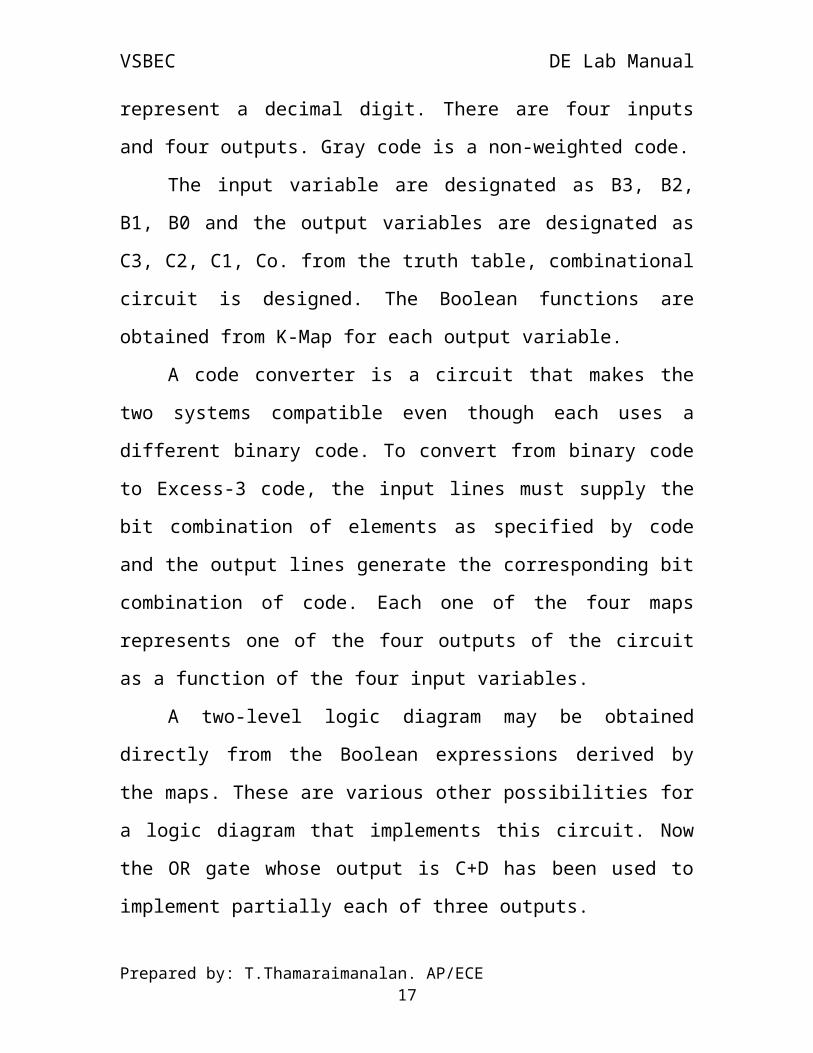
THEORY:The availability of large variety of codes for the same discrete
elements of information results in the use of different codes by different
systems. A conversion circuit must be inserted between the two systems if
each uses different codes for same information. Thus, code converter is a
circuit that makes the two systems compatible even though each uses
different binary code.
The bit combination assigned to binary code to gray code. Since each
code uses four bits to represent a decimal digit. There are four inputs and
four outputs. Gray code is a non-weighted code.
The input variable are designated as B3, B2, B1, B0 and the output
variables are designated as C3, C2, C1, Co. from the truth table,
Prepared by: T.Thamaraimanalan. AP/ECE 12

VSBEC DE Lab Manual
combinational circuit is designed. The Boolean functions are obtained from
K-Map for each output variable.
A code converter is a circuit that makes the two systems compatible
even though each uses a different binary code. To convert from binary code
to Excess-3 code, the input lines must supply the bit combination of
elements as specified by code and the output lines generate the
corresponding bit combination of code. Each one of the four maps represents
one of the four outputs of the circuit as a function of the four input variables.
A two-level logic diagram may be obtained directly from the Boolean
expressions derived by the maps. These are various other possibilities for a
logic diagram that implements this circuit. Now the OR gate whose output is
C+D has been used to implement partially each of three outputs.
LOGIC DIAGRAM:BINARY TO GRAY CODE CONVERTOR
K-Map for G3:
Prepared by: T.Thamaraimanalan. AP/ECE 13

VSBEC DE Lab Manual
G3 = B3
K-Map for G2:
K-Map for G1:
K-Map for G0:
Prepared by: T.Thamaraimanalan. AP/ECE 14

VSBEC DE Lab Manual
TRUTH TABLE:| Binary input | Gray code output |
B3 B2 B1 B0 G3 G2 G1 G0
0000000011111111
0000111100001111
0011001100110011
0101010101010101
0000000011111111
0000111111110000
0011110000111100
0110011001100110
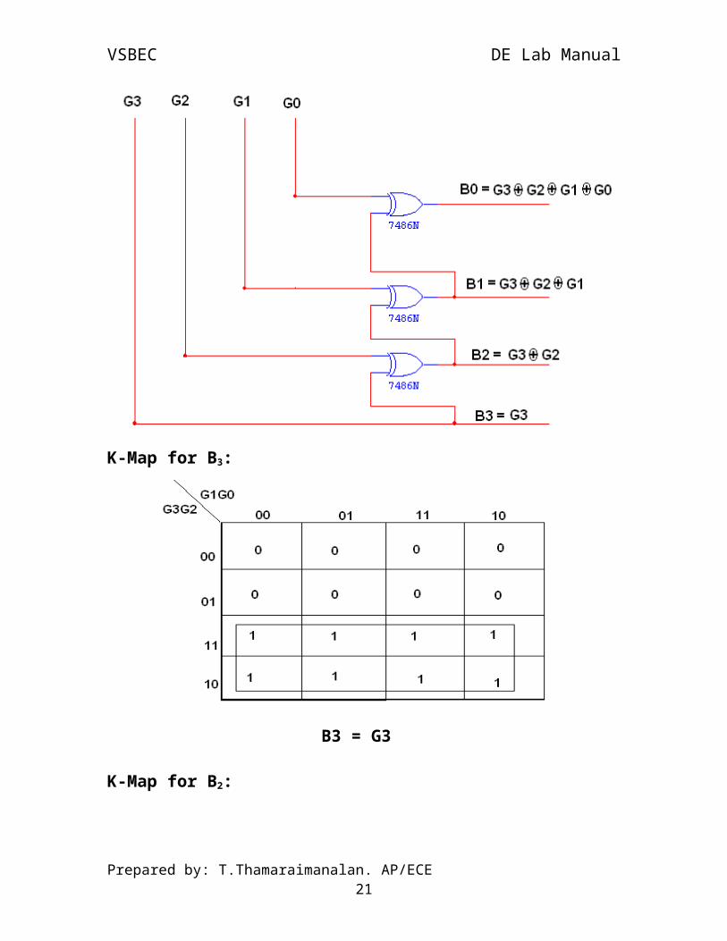
LOGIC DIAGRAM:GRAY CODE TO BINARY CONVERTOR
Prepared by: T.Thamaraimanalan. AP/ECE 15
VSBEC DE Lab Manual
K-Map for B3:
B3 = G3
K-Map for B2:
Prepared by: T.Thamaraimanalan. AP/ECE 16
VSBEC DE Lab Manual
K-Map for B1:
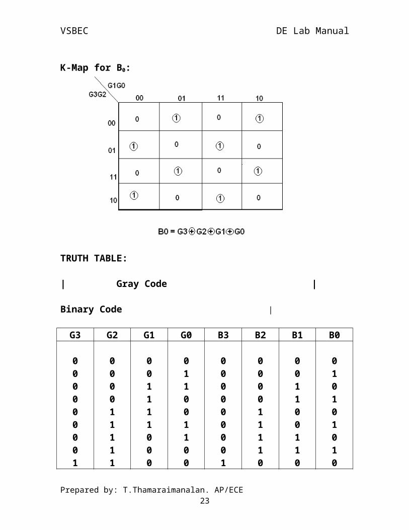
K-Map for B0:
Prepared by: T.Thamaraimanalan. AP/ECE 17

VSBEC DE Lab Manual
TRUTH TABLE:
| Gray Code | Binary Code |
G3 G2 G1 G0 B3 B2 B1 B0
0000000011111111
0000111111110000
0011110000111100
0110011001100110
0000000011111111
0000111100001111
0011001100110011
0101010101010101
Prepared by: T.Thamaraimanalan. AP/ECE 18

VSBEC DE Lab Manual
LOGIC DIAGRAM:BCD TO EXCESS-3 CONVERTOR
K-Map for E3:
Prepared by: T.Thamaraimanalan. AP/ECE 19

VSBEC DE Lab Manual
E3 = B3 + B2 (B0 + B1)
K-Map for E2:
K-Map for E1:
Prepared by: T.Thamaraimanalan. AP/ECE 20
VSBEC DE Lab Manual
K-Map for E0:
TRUTH TABLE:| BCD input | Excess – 3 output |
B3 B2 B1 B0 G3 G2 G1 G0
0000000011111111
0000111100001111
0011001100110011
0101010101010101
0000011111xxxxxx
0111100001xxxxxx
1001100110xxxxxx
1010101010xxxxxx
Prepared by: T.Thamaraimanalan. AP/ECE 21

VSBEC DE Lab Manual
LOGIC DIAGRAM:
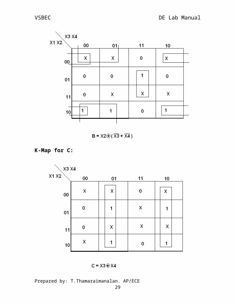
EXCESS-3 TO BCD CONVERTOR
K-Map for A:
A = X1 X2 + X3 X4 X1
Prepared by: T.Thamaraimanalan. AP/ECE 22
VSBEC DE Lab Manual
K-Map for B:
K-Map for C:
Prepared by: T.Thamaraimanalan. AP/ECE 23

VSBEC DE Lab Manual
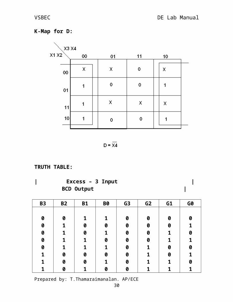
K-Map for D:
TRUTH TABLE:
| Excess – 3 Input | BCD Output |
B3 B2 B1 B0 G3 G2 G1 G0
0000011111
0111100001
1001100110
1010101010
0000000011
0000111100
0011001100
0101010101
Prepared by: T.Thamaraimanalan. AP/ECE 24

VSBEC DE Lab Manual
PROCEDURE:
(i) Connections were given as per circuit diagram.
(ii) Logical inputs were given as per truth table
(iii) Observe the logical output and verify with the truth tables.
RESULT:
Thus the code convertors circuits were designed using logic gates and
their truth table were verified.
Prepared by: T.Thamaraimanalan. AP/ECE 25

VSBEC DE Lab Manual
EXPT NO. : DESIGN OF 4-BIT ADDER AND SUBTRACTORDATE :
AIM: To design and implement 4-bit adder and subtractor using IC 7483.
APPARATUS REQUIRED:Sl.No. COMPONENT SPECIFICATION QTY.
1. IC IC 7483 12. EX-OR GATE IC 7486 13. NOT GATE IC 7404 13. IC TRAINER KIT - 14. PATCH CORDS - 40
THEORY:
4 BIT BINARY ADDER:A binary adder is a digital circuit that produces the arithmetic sum of
two binary numbers. It can be constructed with full adders connected in
cascade, with the output carry from each full adder connected to the input
carry of next full adder in chain. The augends bits of ‘A’ and the addend bits
of ‘B’ are designated by subscript numbers from right to left, with subscript
0 denoting the least significant bits. The carries are connected in chain
through the full adder. The input carry to the adder is C0 and it ripples
through the full adder to the output carry C4.
4 BIT BINARY SUBTRACTOR:
The circuit for subtracting A-B consists of an adder with inverters,
placed between each data input ‘B’ and the corresponding input of full
adder. The input carry C0 must be equal to 1 when performing subtraction.
Prepared by: T.Thamaraimanalan. AP/ECE 26

VSBEC DE Lab Manual
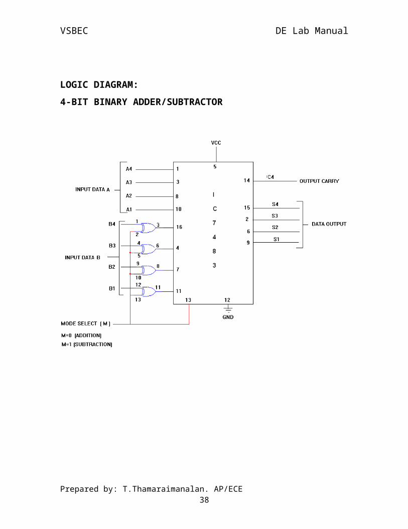
4 BIT BINARY ADDER/SUBTRACTOR:
The addition and subtraction operation can be combined into one
circuit with one common binary adder. The mode input M controls the
operation. When M=0, the circuit is adder circuit. When M=1, it becomes
subtractor.
4 BIT BCD ADDER:
Consider the arithmetic addition of two decimal digits in BCD,
together with an input carry from a previous stage. Since each input digit
does not exceed 9, the output sum cannot be greater than 19, the 1 in the sum
being an input carry. The output of two decimal digits must be represented
in BCD and should appear in the form listed in the columns.
ABCD adder that adds 2 BCD digits and produce a sum digit in BCD.
The 2 decimal digits, together with the input carry, are first added in the top
4 bit adder to produce the binary sum.
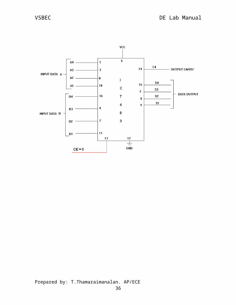
PIN DIAGRAM FOR IC 7483:
Prepared by: T.Thamaraimanalan. AP/ECE 27

VSBEC DE Lab Manual
LOGIC DIAGRAM:4-BIT BINARY ADDER
Prepared by: T.Thamaraimanalan. AP/ECE 28
VSBEC DE Lab Manual
LOGIC DIAGRAM:4-BIT BINARY SUBTRACTOR
Prepared by: T.Thamaraimanalan. AP/ECE 29
VSBEC DE Lab Manual
LOGIC DIAGRAM:4-BIT BINARY ADDER/SUBTRACTOR
Prepared by: T.Thamaraimanalan. AP/ECE 30

VSBEC DE Lab Manual
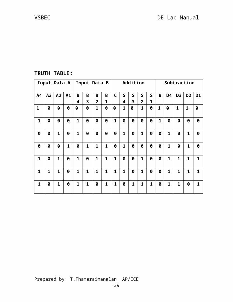
TRUTH TABLE:Input Data A Input Data B Addition Subtraction
A4 A3 A2 A1 B4 B3 B2 B1 C S4 S3 S2 S1 B D4 D3 D2 D1
1 0 0 0 0 0 1 0 0 1 0 1 0 1 0 1 1 0
1 0 0 0 1 0 0 0 1 0 0 0 0 1 0 0 0 0
0 0 1 0 1 0 0 0 0 1 0 1 0 0 1 0 1 0
0 0 0 1 0 1 1 1 0 1 0 0 0 0 1 0 1 0
1 0 1 0 1 0 1 1 1 0 0 1 0 0 1 1 1 1
1 1 1 0 1 1 1 1 1 1 0 1 0 0 1 1 1 1
1 0 1 0 1 1 0 1 1 0 1 1 1 0 1 1 0 1
LOGIC DIAGRAM:BCD ADDER
Prepared by: T.Thamaraimanalan. AP/ECE 31

VSBEC DE Lab Manual
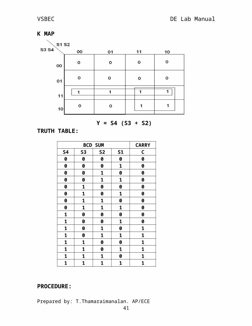
K MAP
Y = S4 (S3 + S2)TRUTH TABLE:
BCD SUM CARRY
Prepared by: T.Thamaraimanalan. AP/ECE 32
VSBEC DE Lab Manual
S4 S3 S2 S1 C0 0 0 0 00 0 0 1 00 0 1 0 00 0 1 1 00 1 0 0 00 1 0 1 00 1 1 0 00 1 1 1 01 0 0 0 01 0 0 1 01 0 1 0 11 0 1 1 11 1 0 0 11 1 0 1 11 1 1 0 11 1 1 1 1
PROCEDURE:
(i) Connections were given as per circuit diagram.
(ii) Logical inputs were given as per truth table
(iii) Observe the logical output and verify with the truth tables.
RESULT:
Thus the 4 bit binary adder, 4 bit binary subtractor and BCD adder
were designed using logic gates and their truth table was verified.
Prepared by: T.Thamaraimanalan. AP/ECE 33

VSBEC DE Lab Manual
EXPT NO. : DESIGN AND IMPLEMENTATION OF MAGNITUDE
COMPARATORDATE :
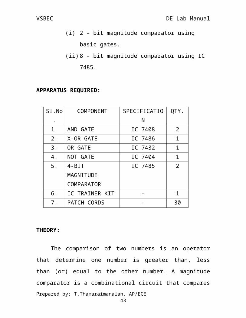
AIM: To design and implement
(i) 2 – bit magnitude comparator using basic gates.
(ii) 8 – bit magnitude comparator using IC 7485.
APPARATUS REQUIRED:
Sl.No. COMPONENT SPECIFICATION QTY.1. AND GATE IC 7408 22. X-OR GATE IC 7486 13. OR GATE IC 7432 14. NOT GATE IC 7404 15. 4-BIT MAGNITUDE
COMPARATOR IC 7485 2
6. IC TRAINER KIT - 17. PATCH CORDS - 30
THEORY:
The comparison of two numbers is an operator that determine one
number is greater than, less than (or) equal to the other number. A
magnitude comparator is a combinational circuit that compares two numbers
A and B and determine their relative magnitude. The outcome of the
comparator is specified by three binary variables that indicate whether A>B,
A=B (or) A<B.
Prepared by: T.Thamaraimanalan. AP/ECE 34

VSBEC DE Lab Manual
A = A3 A2 A1 A0
B = B3 B2 B1 B0
The equality of the two numbers and B is displayed in a
combinational circuit designated by the symbol (A=B).
This indicates A greater than B, then inspect the relative magnitude of
pairs of significant digits starting from most significant position. A is 0 and
that of B is 0.
We have A<B, the sequential comparison can be expanded as
A>B = A3B31 + X3A2B2
1 + X3X2A1B11 + X3X2X1A0B0
1
A<B = A31B3 + X3A2
1B2 + X3X2A11B1 + X3X2X1A0
1B0
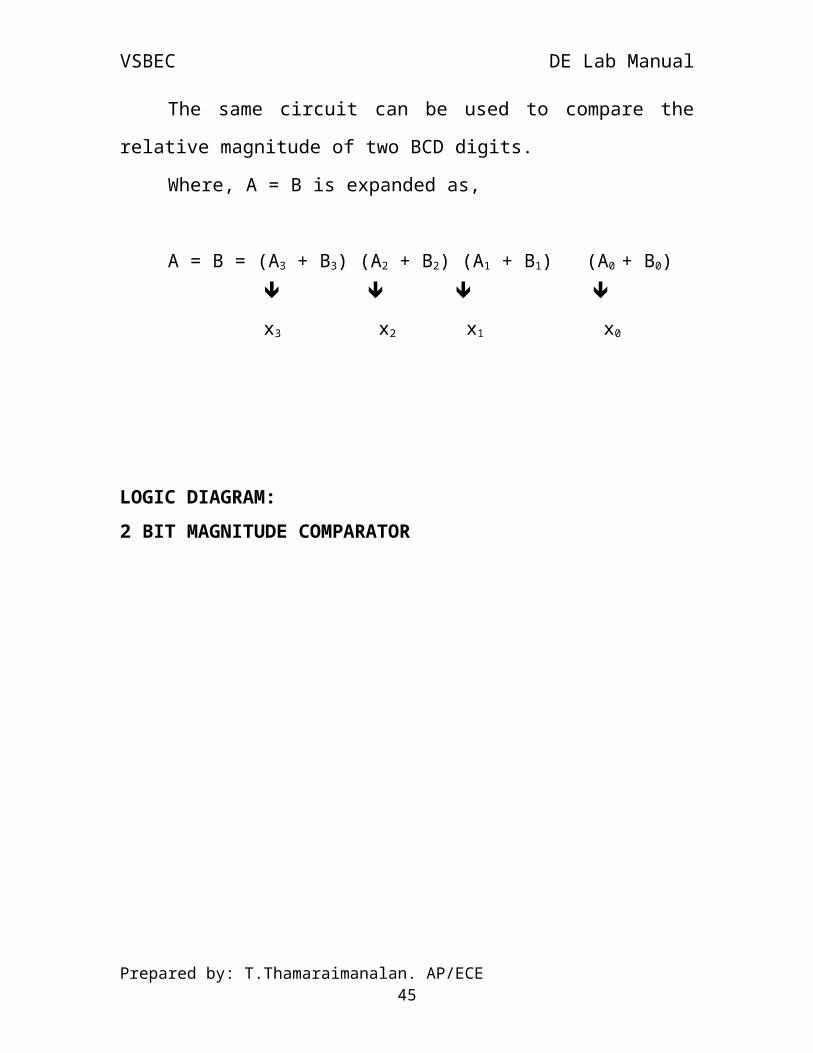
The same circuit can be used to compare the relative magnitude of
two BCD digits.
Where, A = B is expanded as,
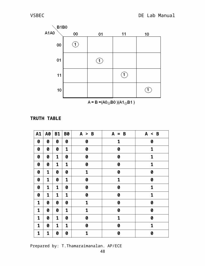
A = B = (A3 + B3) (A2 + B2) (A1 + B1) (A0 + B0)
x3 x2 x1 x0
Prepared by: T.Thamaraimanalan. AP/ECE 35
VSBEC DE Lab Manual
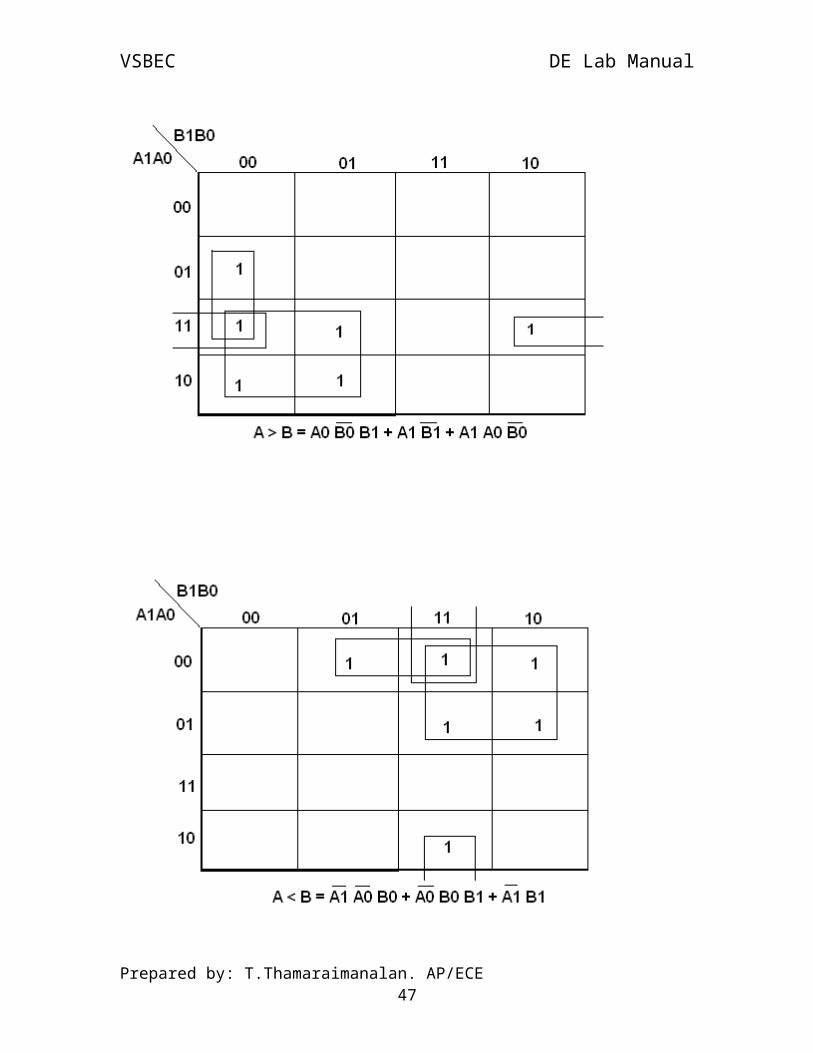
LOGIC DIAGRAM:2 BIT MAGNITUDE COMPARATOR
Prepared by: T.Thamaraimanalan. AP/ECE 36

VSBEC DE Lab Manual
K MAP
Prepared by: T.Thamaraimanalan. AP/ECE 37
VSBEC DE Lab Manual
TRUTH TABLE
A1 A0 B1 B0 A > B A = B A < B0 0 0 0 0 1 00 0 0 1 0 0 10 0 1 0 0 0 10 0 1 1 0 0 10 1 0 0 1 0 00 1 0 1 0 1 00 1 1 0 0 0 10 1 1 1 0 0 11 0 0 0 1 0 01 0 0 1 1 0 01 0 1 0 0 1 01 0 1 1 0 0 11 1 0 0 1 0 01 1 0 1 1 0 01 1 1 0 1 0 01 1 1 1 0 1 0
Prepared by: T.Thamaraimanalan. AP/ECE 38
VSBEC DE Lab Manual
PIN DIAGRAM FOR IC 7485:
Prepared by: T.Thamaraimanalan. AP/ECE 39

VSBEC DE Lab Manual
LOGIC DIAGRAM:8 BIT MAGNITUDE COMPARATOR
TRUTH TABLE:
A B A>B A=B A<B0 0 0 0 0 0 0 0 0 0 0 0 0 0 0 0 0 1 00 0 0 1 0 0 0 1 0 0 0 0 0 0 0 0 1 0 00 0 0 0 0 0 0 0 0 0 0 1 0 0 0 1 0 0 1
Prepared by: T.Thamaraimanalan. AP/ECE 40
VSBEC DE Lab Manual
PROCEDURE:
(i) Connections are given as per circuit diagram.
(ii) Logical inputs are given as per circuit diagram.
(iii) Observe the output and verify the truth table.
RESULT:
Thus the magnitude comparator circuit was designed using logic gates
and their truth table was verified.
Prepared by: T.Thamaraimanalan. AP/ECE 41

VSBEC DE Lab Manual
EXPT NO. : 16 BIT ODD/EVEN PARITY CHECKER /GENERATORDATE :
AIM: To design and implement 16 bit odd/even parity checker generator
using IC 74180.
APPARATUS REQUIRED:
Sl.No. COMPONENT SPECIFICATION QTY.1. NOT GATE IC 7404 11. IC 74180 22. IC TRAINER KIT - 13. PATCH CORDS - 30
THEORY:
A parity bit is used for detecting errors during transmission of binary
information. A parity bit is an extra bit included with a binary message to
make the number is either even or odd. The message including the parity bit
is transmitted and then checked at the receiver ends for errors. An error is
detected if the checked parity bit doesn’t correspond to the one transmitted.
The circuit that generates the parity bit in the transmitter is called a ‘parity
generator’ and the circuit that checks the parity in the receiver is called a
‘parity checker’.
In even parity, the added parity bit will make the total number is even
amount. In odd parity, the added parity bit will make the total number is odd
amount. The parity checker circuit checks for possible errors in the
Prepared by: T.Thamaraimanalan. AP/ECE 42
VSBEC DE Lab Manual
transmission. If the information is passed in even parity, then the bits
required must have an even number of 1’s. An error occur during
transmission, if the received bits have an odd number of 1’s indicating that
one bit has changed in value during transmission.
PIN DIAGRAM FOR IC 74180:
FUNCTION TABLE:INPUTS OUTPUTS
Number of High DataInputs (I0 – I7)
PE PO ∑E ∑O
EVEN 1 0 1 0ODD 1 0 0 1
EVEN 0 1 0 1ODD 0 1 1 0
X 1 1 0 0X 0 0 1 1
Prepared by: T.Thamaraimanalan. AP/ECE 43

VSBEC DE Lab Manual
LOGIC DIAGRAM:
16 BIT ODD/EVEN PARITY CHECKER
TRUTH TABLE:
I7 I6 I5 I4 I3 I2 I1 I0 I7’I6’I5’I4’I3’I2’11’ I0’ Active ∑E ∑O0 0 0 0 0 0 0 1 0 0 0 0 0 0 0 0 1 1 00 0 0 0 0 1 1 0 0 0 0 0 0 1 1 0 0 1 00 0 0 0 0 1 1 0 0 0 0 0 0 1 1 0 1 0 1
Prepared by: T.Thamaraimanalan. AP/ECE 44
VSBEC DE Lab Manual
LOGIC DIAGRAM:16 BIT ODD/EVEN PARITY GENERATOR
TRUTH TABLE:
I7 I6 I5 I4 I3 I2 I1 I0 I7 I6 I5 I4 I3 I2 I1 I0 Active ∑E ∑O1 1 0 0 0 0 0 0 1 1 0 0 0 0 0 0 1 1 01 1 0 0 0 0 0 0 1 1 0 0 0 0 0 0 0 0 11 1 0 0 0 0 0 0 0 1 0 0 0 0 0 0 0 1 0
Prepared by: T.Thamaraimanalan. AP/ECE 45

VSBEC DE Lab Manual
PROCEDURE:
(i) Connections are given as per circuit diagram.
(ii) Logical inputs are given as per circuit diagram.
(iii) Observe the output and verify the truth table.
RESULT:
Thus the parity checker and parity generator circuit was designed
using logic gates and their truth table was verified.
Prepared by: T.Thamaraimanalan. AP/ECE 46
VSBEC DE Lab Manual
EXPT NO. : DESIGN AND IMPLEMENTATION OF MULTIPLEXER AND DEMULTIPLEXER
DATE :
AIM: To design and implement multiplexer and demultiplexer using logic
gates.
APPARATUS REQUIRED:
Sl.No. COMPONENT SPECIFICATION QTY.1. 3 I/P AND GATE IC 7411 22. OR GATE IC 7432 13. NOT GATE IC 7404 12. IC TRAINER KIT - 13. PATCH CORDS - 32
THEORY:MULTIPLEXER:
Multiplexer means transmitting a large number of information units
over a smaller number of channels or lines. A digital multiplexer is a
combinational circuit that selects binary information from one of many input
lines and directs it to a single output line. The selection of a particular input
line is controlled by a set of selection lines. Normally there are 2n input line
and n selection lines whose bit combination determine which input is
selected.
DEMULTIPLEXER:
The function of Demultiplexer is in contrast to multiplexer function. It
takes information from one line and distributes it to a given number of
Prepared by: T.Thamaraimanalan. AP/ECE 47
VSBEC DE Lab Manual
output lines. For this reason, the demultiplexer is also known as a data
distributor. Decoder can also be used as demultiplexer.
In the 1: 4 demultiplexer circuit, the data input line goes to all of the
AND gates. The data select lines enable only one gate at a time and the data
on the data input line will pass through the selected gate to the associated
data output line.
BLOCK DIAGRAM FOR 4:1 MULTIPLEXER:
FUNCTION TABLE:
S1 S0 INPUTS Y
0 0 D0 → D0 S1’ S0’
0 1 D1 → D1 S1’ S0
1 0 D2 → D2 S1 S0’
1 1 D3 → D3 S1 S0
Y = D0 S1’ S0’ + D1 S1’ S0 + D2 S1 S0’ + D3 S1 S0
Prepared by: T.Thamaraimanalan. AP/ECE 48

VSBEC DE Lab Manual
CIRCUIT DIAGRAM FOR MULTIPLEXER:
TRUTH TABLE:
S1 S0 Y = OUTPUT
0 0 D0
0 1 D1
1 0 D2
1 1 D3
Prepared by: T.Thamaraimanalan. AP/ECE 49

VSBEC DE Lab Manual
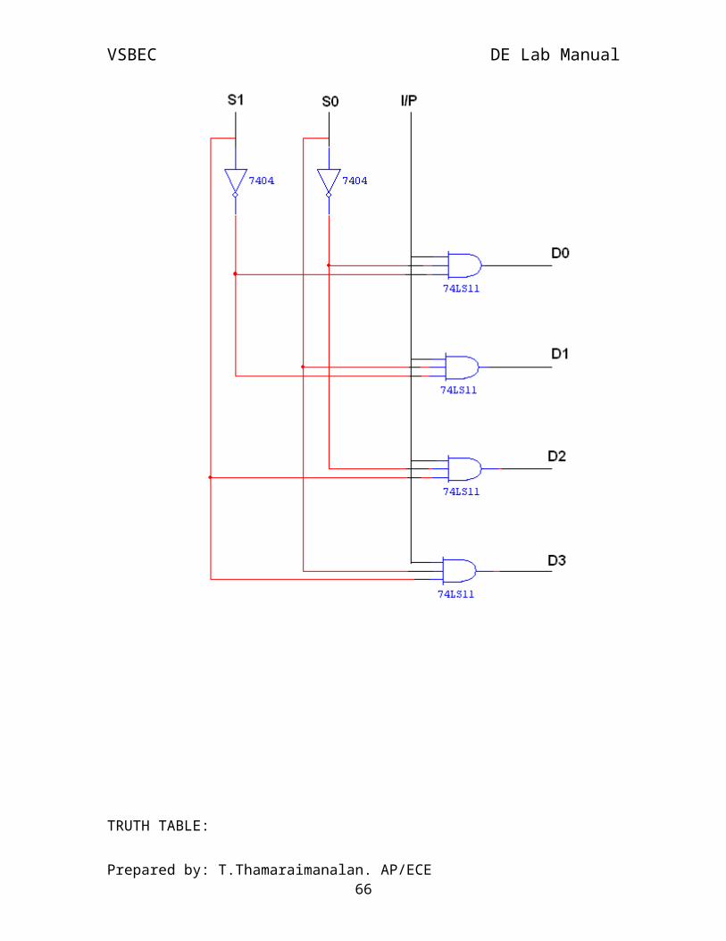
BLOCK DIAGRAM FOR 1:4 DEMULTIPLEXER:
FUNCTION TABLE:
S1 S0 INPUT
0 0 X → D0 = X S1’ S0’
0 1 X → D1 = X S1’ S0
1 0 X → D2 = X S1 S0’
1 1 X → D3 = X S1 S0
Y = X S1’ S0’ + X S1’ S0 + X S1 S0’ + X S1 S0
Prepared by: T.Thamaraimanalan. AP/ECE 50

VSBEC DE Lab Manual
LOGIC DIAGRAM FOR DEMULTIPLEXER:
Prepared by: T.Thamaraimanalan. AP/ECE 51

VSBEC DE Lab Manual
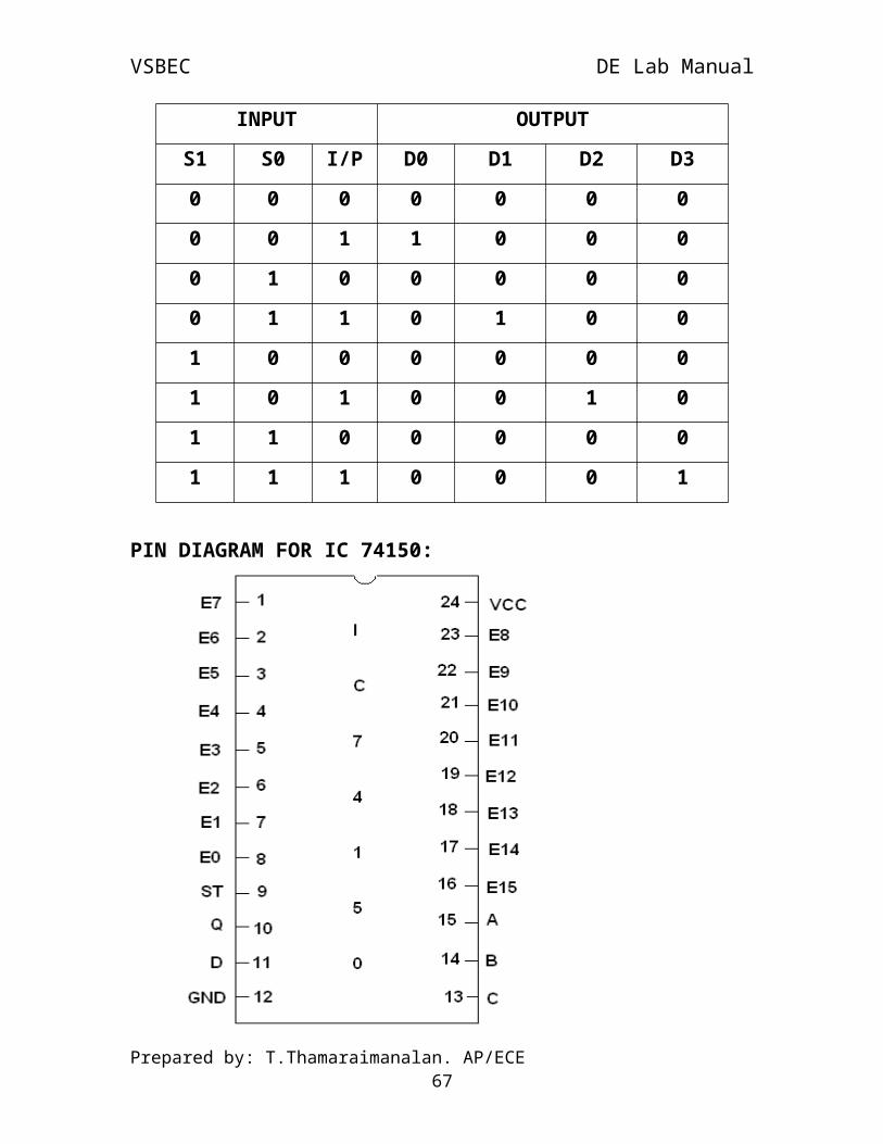
TRUTH TABLE:
INPUT OUTPUT
S1 S0 I/P D0 D1 D2 D3
0 0 0 0 0 0 0
0 0 1 1 0 0 0
0 1 0 0 0 0 0
0 1 1 0 1 0 0
1 0 0 0 0 0 0
1 0 1 0 0 1 0
1 1 0 0 0 0 0
1 1 1 0 0 0 1
PIN DIAGRAM FOR IC 74150:
Prepared by: T.Thamaraimanalan. AP/ECE 52

VSBEC DE Lab Manual
PIN DIAGRAM FOR IC 74154:
PROCEDURE:(i) Connections are given as per circuit diagram.
(ii) Logical inputs are given as per circuit diagram.
(iii) Observe the output and verify the truth table.
RESULT:
Thus the multiplexer and de-multiplexer circuit was designed using
logic gates and their truth table was verified.
EXPT NO. : DESIGN AND IMPLEMENTATION OF ENCODE AND
Prepared by: T.Thamaraimanalan. AP/ECE 53

VSBEC DE Lab Manual
DECODERDATE :
AIM: To design and implement encoder and decoder using logic gates.
APPARATUS REQUIRED:
Sl.No. COMPONENT SPECIFICATION QTY.1. 3 I/P NAND GATE IC 7410 22. OR GATE IC 7432 33. NOT GATE IC 7404 12. IC TRAINER KIT - 13. PATCH CORDS - 27
THEORY:
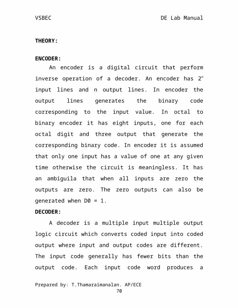
ENCODER:An encoder is a digital circuit that perform inverse operation of a
decoder. An encoder has 2n input lines and n output lines. In encoder the
output lines generates the binary code corresponding to the input value. In
octal to binary encoder it has eight inputs, one for each octal digit and three
output that generate the corresponding binary code. In encoder it is assumed
that only one input has a value of one at any given time otherwise the circuit
is meaningless. It has an ambiguila that when all inputs are zero the outputs
are zero. The zero outputs can also be generated when D0 = 1.
DECODER:
A decoder is a multiple input multiple output logic circuit which
converts coded input into coded output where input and output codes are
different. The input code generally has fewer bits than the output code. Each
Prepared by: T.Thamaraimanalan. AP/ECE 54

VSBEC DE Lab Manual
input code word produces a different output code word i.e there is one to one
mapping can be expressed in truth table. In the block diagram of decoder
circuit the encoded information is present as n input producing 2n possible
outputs. 2n output values are from 0 through out 2n – 1.
PIN DIAGRAM FOR IC 7445:
BCD TO DECIMAL DECODER:
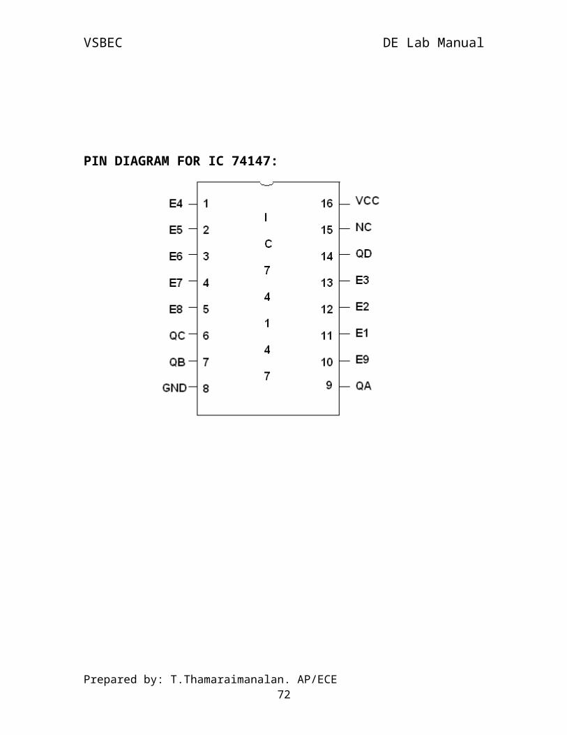
PIN DIAGRAM FOR IC 74147:
Prepared by: T.Thamaraimanalan. AP/ECE 55

VSBEC DE Lab Manual
LOGIC DIAGRAM FOR ENCODER:
Prepared by: T.Thamaraimanalan. AP/ECE 56

VSBEC DE Lab Manual
TRUTH TABLE:
INPUT OUTPUT
Y1 Y2 Y3 Y4 Y5 Y6 Y7 A B C
1 0 0 0 0 0 0 0 0 1
0 1 0 0 0 0 0 0 1 0
0 0 1 0 0 0 0 0 1 1
0 0 0 1 0 0 0 1 0 0
0 0 0 0 1 0 0 1 0 1
0 0 0 0 0 1 0 1 1 0
0 0 0 0 0 0 1 1 1 1
LOGIC DIAGRAM FOR DECODER:
Prepared by: T.Thamaraimanalan. AP/ECE 57
VSBEC DE Lab Manual
TRUTH TABLE:
INPUT OUTPUT
E A B D0 D1 D2 D3
1 0 0 1 1 1 1
0 0 0 0 1 1 1
0 0 1 1 0 1 1
0 1 0 1 1 0 1
0 1 1 1 1 1 0
Prepared by: T.Thamaraimanalan. AP/ECE 58

VSBEC DE Lab Manual
PROCEDURE:
(i) Connections are given as per circuit diagram.
(ii) Logical inputs are given as per circuit diagram.
(iii) Observe the output and verify the truth table.
RESULT:
Thus the encoder and decoder circuit was designed using logic gates
and their truth table was verified.
Prepared by: T.Thamaraimanalan. AP/ECE 59

VSBEC DE Lab Manual
EXPT NO. : CONSTRUCTION AND VERIFICATION OF 4 BITRIPPLE COUNTER AND MOD 10/MOD 12 RIPPLE COUNTER
DATE :
AIM: To design and verify 4 bit ripple counter mod 10/ mod 12 ripple
counter.
APPARATUS REQUIRED:
Sl.No. COMPONENT SPECIFICATION QTY.1. JK FLIP FLOP IC 7476 22. NAND GATE IC 7400 13. IC TRAINER KIT - 14. PATCH CORDS - 30
THEORY:
A counter is a register capable of counting number of clock pulse
arriving at its clock input. Counter represents the number of clock pulses
arrived. A specified sequence of states appears as counter output. This is the
main difference between a register and a counter. There are two types of
counter, synchronous and asynchronous. In synchronous common clock is
given to all flip flop and in asynchronous first flip flop is clocked by external
pulse and then each successive flip flop is clocked by Q or Q output of
previous stage. A soon the clock of second stage is triggered by output of
first stage. Because of inherent propagation delay time all flip flops are not
activated at same time which results in asynchronous operation.
Prepared by: T.Thamaraimanalan. AP/ECE 60

VSBEC DE Lab Manual
PIN DIAGRAM FOR IC 7476:
LOGIC DIAGRAM FOR 4 BIT RIPPLE COUNTER:
Prepared by: T.Thamaraimanalan. AP/ECE 61

VSBEC DE Lab Manual
TRUTH TABLE:
CLK QA QB QC QD
0 0 0 0 0
1 1 0 0 0
2 0 1 0 0
3 1 1 0 0
4 0 0 1 0
5 1 0 1 0
6 0 1 1 0
7 1 1 1 0
8 0 0 0 1
9 1 0 0 1
10 0 1 0 1
11 1 1 0 1
12 0 0 1 1
13 1 0 1 1
14 0 1 1 1
15 1 1 1 1
Prepared by: T.Thamaraimanalan. AP/ECE 62

VSBEC DE Lab Manual
LOGIC DIAGRAM FOR MOD - 10 RIPPLE COUNTER:
TRUTH TABLE:
CLK QA QB QC QD
0 0 0 0 0
1 1 0 0 0
2 0 1 0 0
3 1 1 0 0
4 0 0 1 0
5 1 0 1 0
6 0 1 1 0
7 1 1 1 0
8 0 0 0 1
9 1 0 0 1
10 0 0 0 0
Prepared by: T.Thamaraimanalan. AP/ECE 63

VSBEC DE Lab Manual
LOGIC DIAGRAM FOR MOD - 12 RIPPLE COUNTER:
TRUTH TABLE:
CLK QA QB QC QD
0 0 0 0 0
1 1 0 0 0
2 0 1 0 0
3 1 1 0 0
4 0 0 1 0
5 1 0 1 0
6 0 1 1 0
7 1 1 1 0
8 0 0 0 1
9 1 0 0 1
10 0 1 0 1
11 1 1 0 1
12 0 0 0 0
PROCEDURE:
Prepared by: T.Thamaraimanalan. AP/ECE 64

VSBEC DE Lab Manual
(i) Connections are given as per circuit diagram.
(ii) Logical inputs are given as per circuit diagram.
(iii) Observe the output and verify the truth table.
RESULT:
Thus the 4 bit ripple counter and mod 10 ripple counter circuit was
designed using logic gates and their truth table was verified.
Prepared by: T.Thamaraimanalan. AP/ECE 65
VSBEC DE Lab Manual
EXPT NO. : DESIGN AND IMPLEMENTATION OF 3 BIT SYNCHRONOUS
UP AND DOWN COUNTERDATE :
AIM: To design and implement 3 bit synchronous up and down counter.
APPARATUS REQUIRED:
Sl.No. COMPONENT SPECIFICATION QTY.1. JK FLIP FLOP IC 7476 22. 3 I/P AND GATE IC 7411 13. OR GATE IC 7432 14. XOR GATE IC 7486 15. NOT GATE IC 7404 16. IC TRAINER KIT - 17. PATCH CORDS - 35
THEORY:
A counter is a register capable of counting number of clock pulse
arriving at its clock input. Counter represents the number of clock pulses
arrived. An up/down counter is one that is capable of progressing in
increasing order or decreasing order through a certain sequence. An up/down
counter is also called bidirectional counter. Usually up/down operation of
the counter is controlled by up/down signal. When this signal is high counter
goes through up sequence and when up/down signal is low counter follows
reverse sequence.
Prepared by: T.Thamaraimanalan. AP/ECE 66
VSBEC DE Lab Manual
LOGIC DIAGRAM:
TRUTH TABLE:CLK QA QB QC QN
0 0 0 0 01 0 0 0 12 0 0 1 03 0 0 1 14 0 1 0 05 0 1 0 16 0 1 1 07 0 1 1 18 1 0 0 09 1 0 0 110 1 0 1 011 1 0 1 112 1 1 0 013 1 1 0 114 1 1 1 015 1 1 1 1
Prepared by: T.Thamaraimanalan. AP/ECE 67

VSBEC DE Lab Manual
LOGIC DIAGRAM FOR DOWN COUNTER
TRUTH TABLE
Clock Output0 00001 00012 00103 00114 01005 01016 01107 01118 10009 100110 101011 101112 110013 110114 111015 1111
Prepared by: T.Thamaraimanalan. AP/ECE 68
VSBEC DE Lab Manual
PROCEDURE:(i) Connections are given as per circuit diagram.
(ii) Logical inputs are given as per circuit diagram.
(iii) Observe the output and verify the truth table.
RESULT:
Thus Up counter and Down counter was designed successfully using
IC 7476 and its truth table was verified successfully.
Prepared by: T.Thamaraimanalan. AP/ECE 69
VSBEC DE Lab Manual
EXPT NO. : DESIGN AND IMPLEMENTATION OF SHIFT REGISTERDATE :
AIM: To design and implement (i) Serial in serial out (ii) Serial in parallel out (iii) Parallel in serial out (iv) Parallel in parallel out
APPARATUS REQUIRED:
Sl.No. COMPONENT SPECIFICATION QTY.1. D FLIP FLOP IC 7474 22. OR GATE IC 7432 13. IC TRAINER KIT - 14. PATCH CORDS - 35
THEORY:
A register is capable of shifting its binary information in one or both
directions is known as shift register. The logical configuration of shift
register consist of a D-Flip flop cascaded with output of one flip flop
connected to input of next flip flop. All flip flops receive common clock
pulses which causes the shift in the output of the flip flop. The simplest
possible shift register is one that uses only flip flop. The output of a given
flip flop is connected to the input of next flip flop of the register. Each clock
pulse shifts the content of register one bit position to right.
Prepared by: T.Thamaraimanalan. AP/ECE 70

VSBEC DE Lab Manual
PIN DIAGRAM:
LOGIC DIAGRAM:
SERIAL IN SERIAL OUT:
Prepared by: T.Thamaraimanalan. AP/ECE 71
VSBEC DE Lab Manual
TRUTH TABLE:
CLK
Serial in Serial out
1 1 0
2 0 0
3 0 0
4 1 1
5 X 0
6 X 0
7 X 1
LOGIC DIAGRAM:
SERIAL IN PARALLEL OUT:
TRUTH TABLE:
CLK DATA
OUTPUT
QA QB QC QD
1 1 1 0 0 0
2 0 0 1 0 0
3 0 0 0 1 1
4 1 1 0 0 1
Prepared by: T.Thamaraimanalan. AP/ECE 72

VSBEC DE Lab Manual
LOGIC DIAGRAM:
PARALLEL IN SERIAL OUT:
TRUTH TABLE:
CLK Q3 Q2 Q1 Q0 O/P
0 1 0 0 1 1
1 0 0 0 0 0
2 0 0 0 0 0
3 0 0 0 0 1
LOGIC DIAGRAM:
PARALLEL IN PARALLEL OUT:
Prepared by: T.Thamaraimanalan. AP/ECE 73
VSBEC DE Lab Manual
TRUTH TABLE:
CLK
DATA INPUT OUTPUT
DA DB DC DD QA QB QC QD
1 1 0 0 1 1 0 0 1
2 1 0 1 0 1 0 1 0
PROCEDURE:
(i) Connections are given as per circuit diagram.
(ii) Logical inputs are given as per circuit diagram.
(iii) Observe the output and verify the truth table.
RESULT:
Thus the various shift registers were designed successfully using flip-
flops and their truth tables were verified successfully.
Prepared by: T.Thamaraimanalan. AP/ECE 74

VSBEC DE Lab Manual
EXPT NO. : DESIGN AND SIMULATION OF COMBINATIONAL AND
SEQUENTIAL CIRCUITSDATE :
AIM: To design and simulate (i) Adder and Subtractor (ii) Multiplexer and De-multiplexer(iii) Ripple counter(iv) Shift registers
TOOLS REQUIRED
XILINX Software
Modelsim simulator
PROCEDURE
Write and draw the Digital logic system. Write the Verilog HDL code for above system. Open project navigator Select File New project Give the file name and press next Give the entity name and select Verilog HDL module and press next Give the inputs and outputs and specify input or output or in-out and
select next Then give finish and the entity and the architecture details appear by
itself Enter the Verilog HDL code in after architecture. Check the syntax and simulate the above Verilog HDL code (using
ModelSim or Xilinx) and verify the output waveform as obtained. Verify the graph with the truth table
Prepared by: T.Thamaraimanalan. AP/ECE 75
VSBEC DE Lab Manual
PROGRAM
HALF ADDER
module half_adder(in_x, in_y, out_sum, out_carry);
input in_x;
input in_y;
output out_sum;
output out_carry;
xor (out_sum, in_x, in_y);
and (out_carry, in_x, in_y);
end module;
FULL ADDER
module full_adder(x, y, z, sum, carry);
input x;
input y;
output sum;
output carry;
wire a, b, c;
xor (sum, x, y, z);
and (a, x, y);
and (b, y, z);
and (c, z, x);
or (carry, a, b, c);
end module;
Prepared by: T.Thamaraimanalan. AP/ECE 76

VSBEC DE Lab Manual
HALF SUBTRACTOR
module half_subtractor (x, y, diff, borrow);
input x;
input y;
output diff;
output borrow;
wire ybar;
not (ybar, y);
xor (diff, x, y);
and (borrow, x, ybar);
end module;
MULTIPLEXER
module mux_4 to 1 ( y, I1, I2, I3, I4, S0, S1);
input I1, I2, I3, I4, S0, S1;
output y;
wire S1bar, S0bar, a, b, c, d;
not (S1bar, S1);
not (S0bar, S0);
and (a, S1bar, S0bar, I1);
and (b, S1bar, S0, I2);
and (c, S1, S0bar, I3);
and (d, S1, S0, I4);
or (y, a, b, c, d);
end module;
Prepared by: T.Thamaraimanalan. AP/ECE 77

VSBEC DE Lab Manual
DE-MULTIPLEXER
module mux_4 to 1 ( Y1, Y2, Y3, Y4, I, S0, S1);
input I, S0, S1;
output Y1, Y2, Y3, Y4;
wire S1bar, S0bar;
not (S1bar, S1);
not (S0bar, S0);
and (Y1, S1bar, S0bar, I);
and (Y2, S1bar, S0, I);
and (Y3, S1, S0bar, I);
and (Y4, S1, S0, I);
or (y, a, b, c, d);
end module;
RIPPLE COUNTER
module counter (count, load, in, clk, clr, a, c);input count, load, clk, clr;input [3:0] in;output c;output [3:0] a;reg [3:0] a;assign c = count & ~load & (a = = 4’b1111);always @ (posedge CLK or negedge clr)if (~clr) A = 4’b0000;else if (load) a = in;else if (count) a = a + 1’b1;else a = a;
end module;
Prepared by: T.Thamaraimanalan. AP/ECE 78
VSBEC DE Lab Manual
SISO SHIFT REGISTER
module shift (clk, SE, SI, SO);input SE, SI;output SO;reg [3:0] temp;always @ (posedge clk)beginif (SE)begintemp = temp << 1;temp[0] = SI;end;beginassign SO = temp [3];
end module;
SIPO SHIFT REGISTER
module shift (clk, SE, SI, PO);input SE, SI;output PO [3:0];reg [3:0] temp;always @ (posedge clk)beginif (SE)begintemp = {temp [2:0], SI};end;beginassign PO = temp;
end module;
Prepared by: T.Thamaraimanalan. AP/ECE 79

VSBEC DE Lab Manual
RESULT:
Thus the simulation of adders, subtractors, multiplexer, de-
multiplexer, ripple counter, shift registers using XILINX software and
simulated their circuit using modelsim simulator.
Prepared by: T.Thamaraimanalan. AP/ECE 80