Embed Size (px)
Citation preview

Dec 21, 2007 DfT@IITK 1
Design for TestabilityDesign for Testability
Virendra SinghIndian Institute of Science
Bangalorevirendra@ {computer, ieee}.org
IEP on Digital System Synthesis
at IIT Kanpur (Dec 11-21, 2007)
Dec 21, 2007 DfT@IITK 2
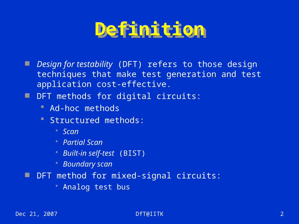
DefinitionDefinition
Design for testability (DFT) refers to those design techniques that make test generation and test application cost-effective.
DFT methods for digital circuits: Ad-hoc methods Structured methods:
Scan Partial Scan Built-in self-test (BIST) Boundary scan
DFT method for mixed-signal circuits: Analog test bus
Dec 21, 2007 DfT@IITK 3
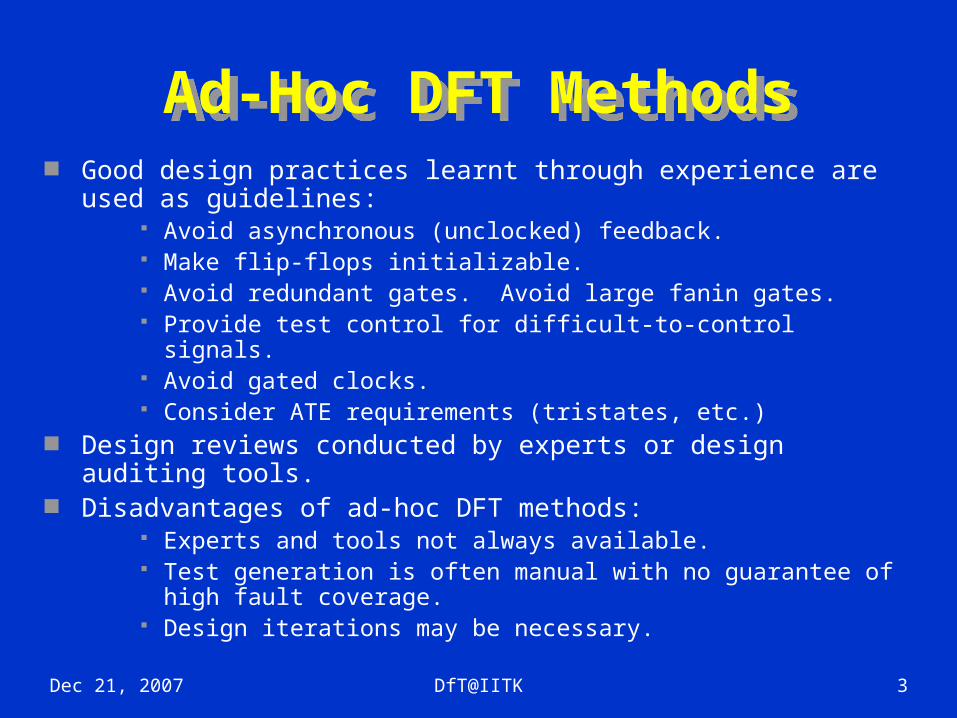
Ad-Hoc DFT MethodsAd-Hoc DFT Methods Good design practices learnt through experience are used as
guidelines: Avoid asynchronous (unclocked) feedback. Make flip-flops initializable. Avoid redundant gates. Avoid large fanin gates. Provide test control for difficult-to-control signals. Avoid gated clocks. Consider ATE requirements (tristates, etc.)
Design reviews conducted by experts or design auditing tools.
Disadvantages of ad-hoc DFT methods: Experts and tools not always available. Test generation is often manual with no guarantee of high
fault coverage. Design iterations may be necessary.
Dec 21, 2007 DfT@IITK 4
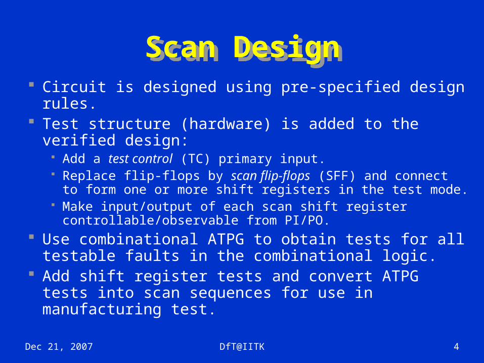
Scan DesignScan Design Circuit is designed using pre-specified design rules. Test structure (hardware) is added to the verified
design: Add a test control (TC) primary input. Replace flip-flops by scan flip-flops (SFF) and connect to
form one or more shift registers in the test mode. Make input/output of each scan shift register
controllable/observable from PI/PO. Use combinational ATPG to obtain tests for all
testable faults in the combinational logic. Add shift register tests and convert ATPG tests into
scan sequences for use in manufacturing test.
Dec 21, 2007 DfT@IITK 5
Scan Design RulesScan Design Rules
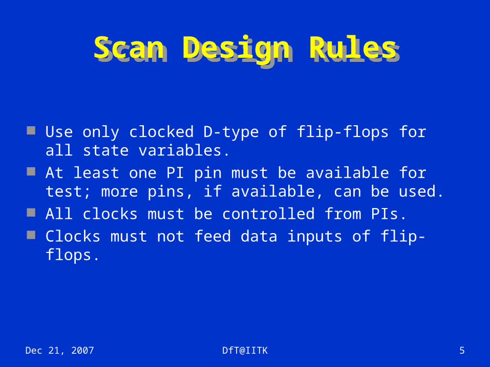
Use only clocked D-type of flip-flops for all state variables.
At least one PI pin must be available for test; more pins, if available, can be used.
All clocks must be controlled from PIs. Clocks must not feed data inputs of flip-flops.
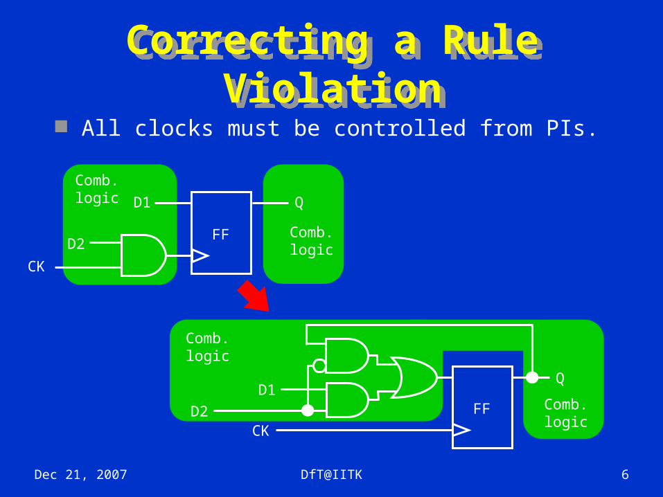
Dec 21, 2007 DfT@IITK 6
Correcting a Rule Violation
Correcting a Rule Violation
All clocks must be controlled from PIs.
Comb.logic
Comb.logic
D1
D2
CK
Q
FF
Comb.logic
D1
D2CK
Q
FF
Comb.logic
Dec 21, 2007 DfT@IITK 7
Scan Flip-Flop (SFF)Scan Flip-Flop (SFF)D
TC
SD
CK
Q
QMUX
D flip-flop
Master latch Slave latch
CK
TC Normal mode, D selected Scan mode, SD selected
Master open Slave opent
t
Logicoverhead
Dec 21, 2007 DfT@IITK 8
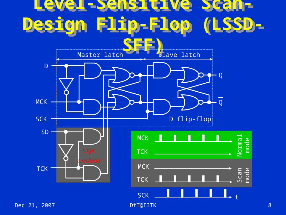
Level-Sensitive Scan-Design Flip-Flop (LSSD-SFF)
Level-Sensitive Scan-Design Flip-Flop (LSSD-SFF)
D
SD
MCK
Q
Q
D flip-flop
Master latch Slave latch
t
SCK
TCK
SCK
MCK
TCK Norm
al
mode
MCK
TCK Sca
nm
ode
Logic
overhead
Dec 21, 2007 DfT@IITK 9
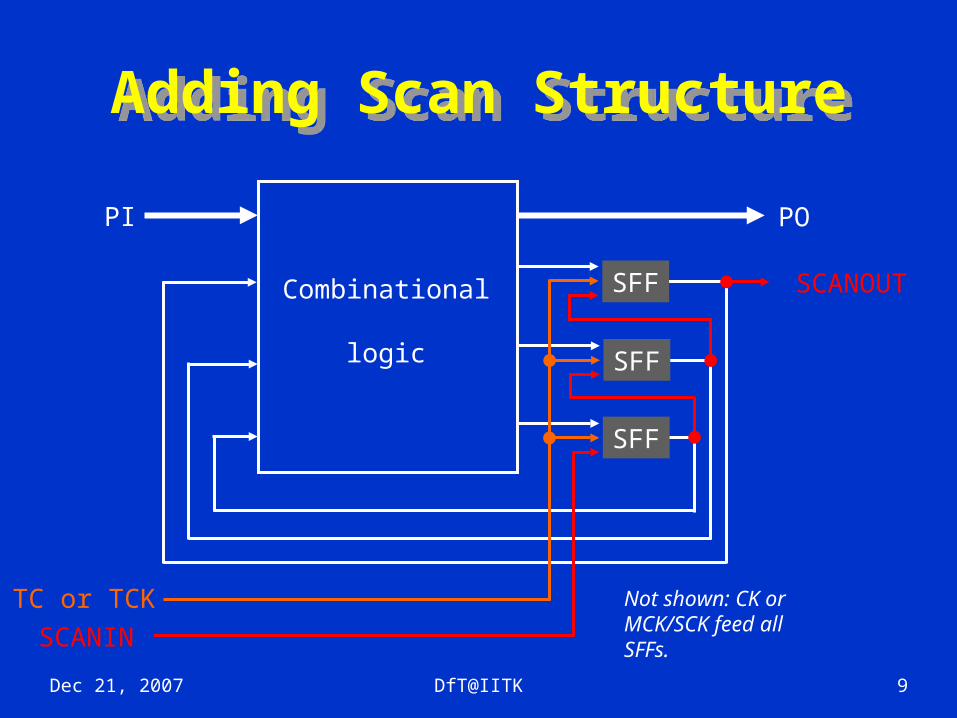
Adding Scan StructureAdding Scan Structure
SFF
SFF
SFF
Combinational
logic
PI PO
SCANOUT
SCANINTC or TCK Not shown: CK or
MCK/SCK feed allSFFs.
Dec 21, 2007 DfT@IITK 10
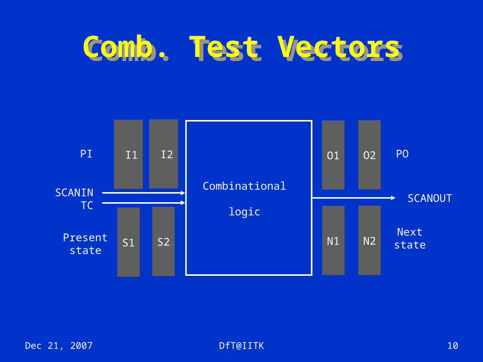
Comb. Test VectorsComb. Test Vectors
I2 I1 O1 O2
S2S1 N2N1
Combinational
logic
PI
Presentstate
PO
Nextstate
SCANINTC
SCANOUT
Dec 21, 2007 DfT@IITK 11
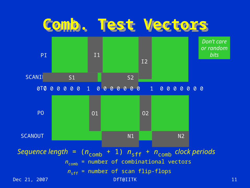
Comb. Test VectorsComb. Test Vectors
I2 I1
O1 O2
PI
PO
SCANIN
SCANOUT
S1 S2
N1 N2
0 0 0 0 0 0 0 1 0 0 0 0 0 0 0 1 0 0 0 0 0 0 0TC
Don’t careor random
bits
Sequence length = (ncomb + 1) nsff + ncomb clock periodsncomb = number of combinational vectors
nsff = number of scan flip-flops
Dec 21, 2007 DfT@IITK 12
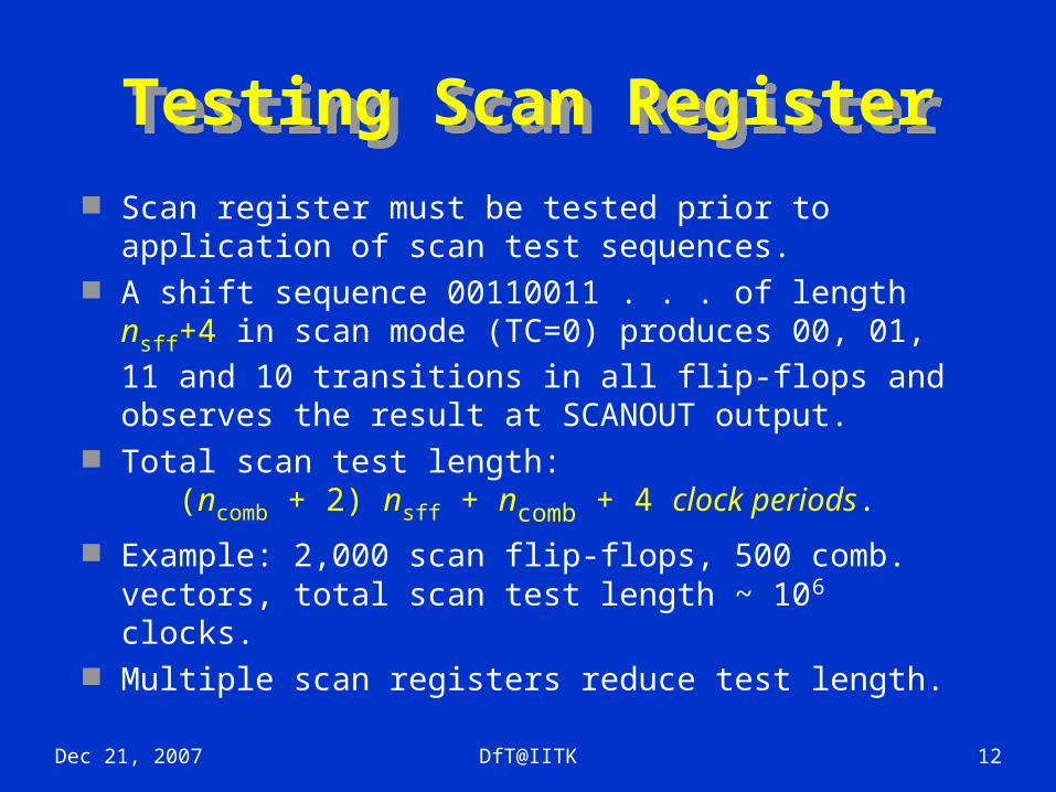
Testing Scan RegisterTesting Scan Register Scan register must be tested prior to
application of scan test sequences. A shift sequence 00110011 . . . of length nsff+4
in scan mode (TC=0) produces 00, 01, 11 and 10 transitions in all flip-flops and observes the result at SCANOUT output.
Total scan test length: (ncomb + 2) nsff + ncomb + 4 clock periods.
Example: 2,000 scan flip-flops, 500 comb. vectors, total scan test length ~ 106 clocks.
Multiple scan registers reduce test length.
Dec 21, 2007 DfT@IITK 13
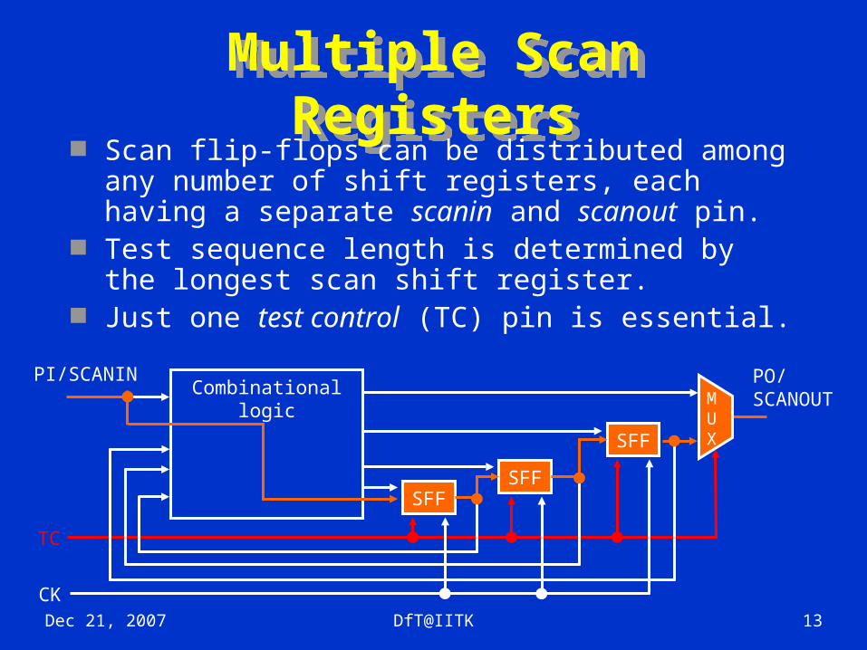
Multiple Scan RegistersMultiple Scan Registers Scan flip-flops can be distributed among any
number of shift registers, each having a separate scanin and scanout pin.
Test sequence length is determined by the longest scan shift register.
Just one test control (TC) pin is essential.
SFFSFF
SFF
Combinationallogic
PI/SCANIN PO/SCANOUTM
UX
CK
TC
Dec 21, 2007 DfT@IITK 14
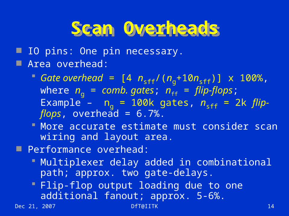
Scan OverheadsScan Overheads IO pins: One pin necessary. Area overhead:
Gate overhead = [4 nsff/(ng+10nsff)] x 100%, where ng = comb. gates; nff = flip-flops; Example – ng = 100k gates, nsff = 2k flip-flops, overhead = 6.7%.
More accurate estimate must consider scan wiring and layout area.
Performance overhead: Multiplexer delay added in combinational path;
approx. two gate-delays. Flip-flop output loading due to one additional
fanout; approx. 5-6%.
Dec 21, 2007 DfT@IITK 15
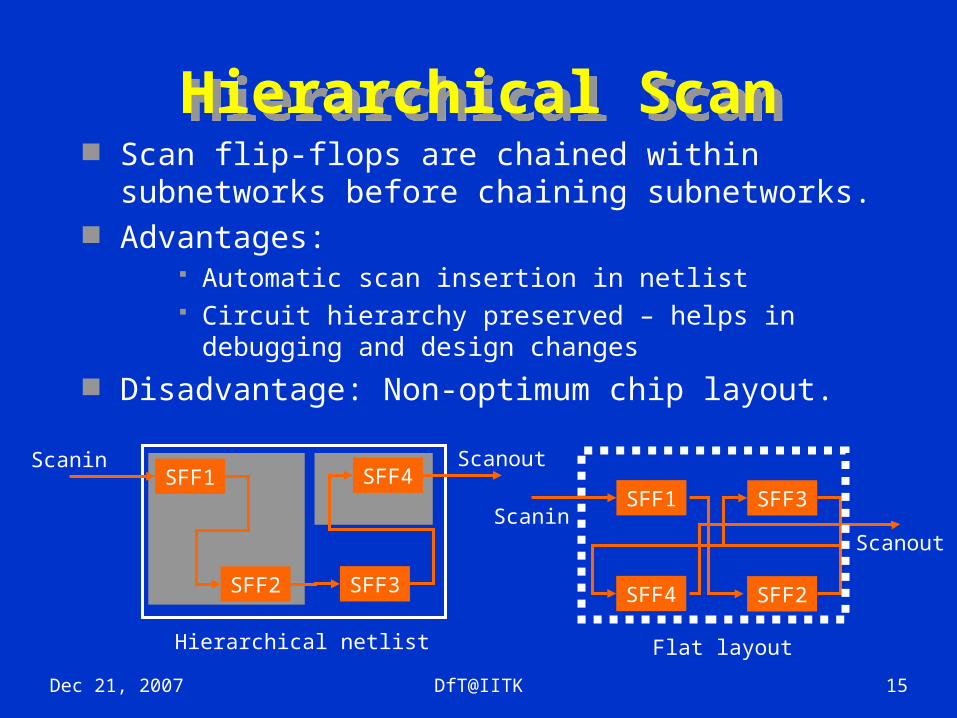
Hierarchical ScanHierarchical Scan Scan flip-flops are chained within subnetworks
before chaining subnetworks. Advantages:
Automatic scan insertion in netlist Circuit hierarchy preserved – helps in debugging
and design changes Disadvantage: Non-optimum chip layout.
SFF1
SFF2 SFF3
SFF4SFF3SFF1
SFF2SFF4
Scanin Scanout
ScaninScanout
Hierarchical netlist Flat layout
Dec 21, 2007 DfT@IITK 16
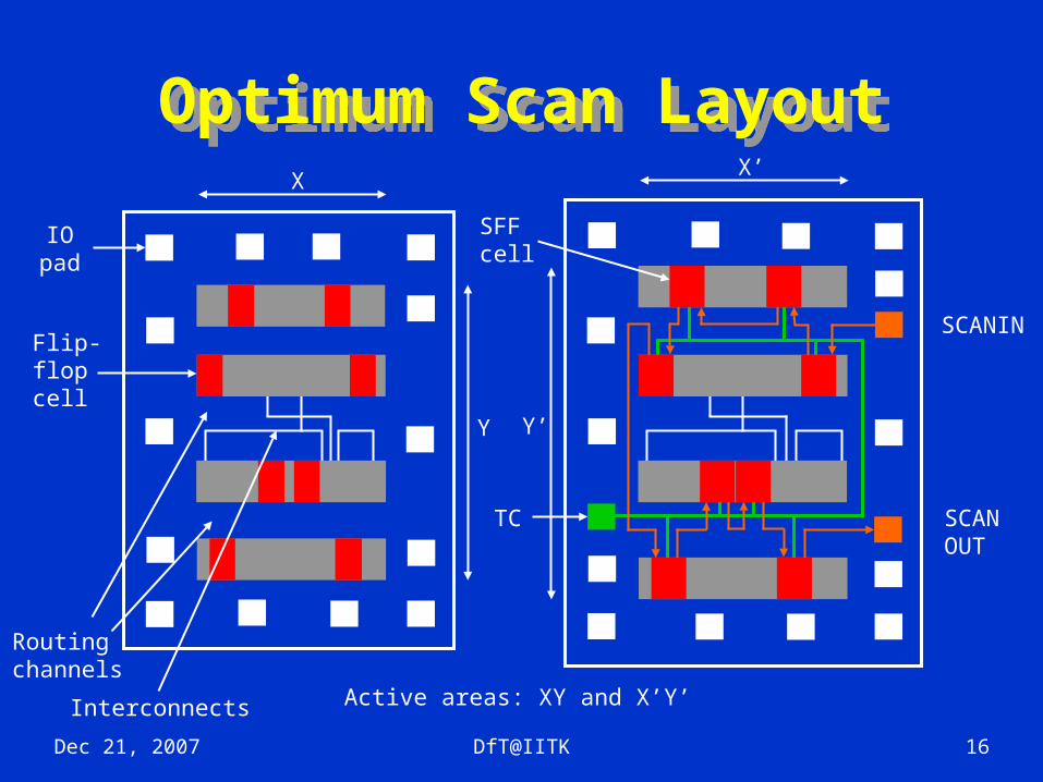
Optimum Scan LayoutOptimum Scan Layout
IOpad
Flip-flopcell
Interconnects
Routingchannels
SFFcell
TC
SCANIN
SCANOUT
Y
XX’
Y’
Active areas: XY and X’Y’
Dec 21, 2007 DfT@IITK 17
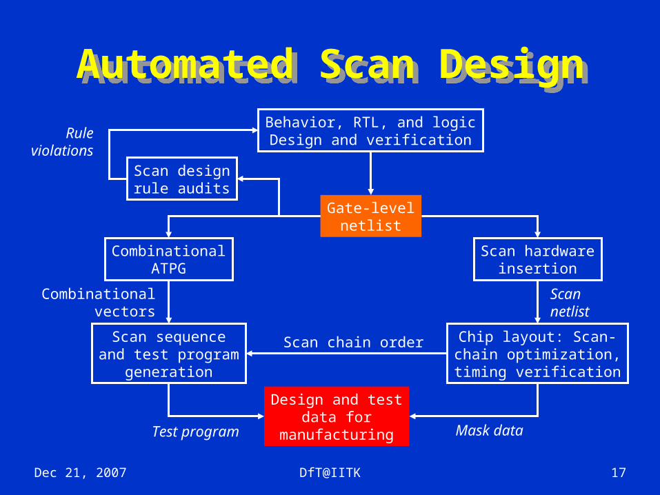
Automated Scan DesignAutomated Scan DesignBehavior, RTL, and logicDesign and verification
Gate-levelnetlist
Scan designrule audits
CombinationalATPG
Scan hardwareinsertion
Chip layout: Scan-chain optimization,timing verification
Scan sequenceand test program
generation
Design and testdata for
manufacturing
Ruleviolations
Scannetlist
Combinationalvectors
Scan chain order
Mask dataTest program
Dec 21, 2007 DfT@IITK 18
Timing and PowerTiming and Power
Small delays in scan path and clock skew can cause race condition.
Large delays in scan path require slower scan clock.
Dynamic multiplexers: Skew between TC and TC signals can cause momentary shorting of D and SD inputs.
Random signal activity in combinational circuit during scan can cause excessive power dissipation.
Dec 21, 2007 DfT@IITK 19
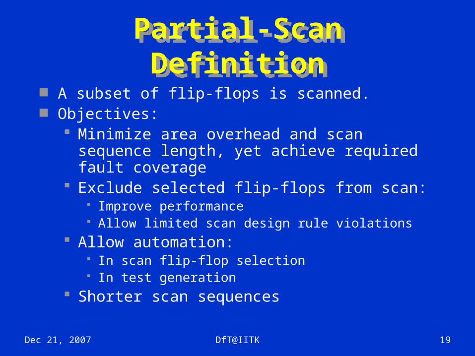
Partial-Scan DefinitionPartial-Scan Definition A subset of flip-flops is scanned. Objectives:
Minimize area overhead and scan sequence length, yet achieve required fault coverage
Exclude selected flip-flops from scan: Improve performance Allow limited scan design rule violations
Allow automation: In scan flip-flop selection In test generation
Shorter scan sequences
Dec 21, 2007 DfT@IITK 20
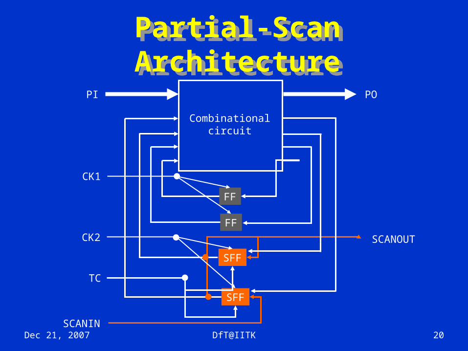
Partial-Scan ArchitecturePartial-Scan Architecture
FF
FF
SFF
SFF
Combinationalcircuit
PI PO
CK1
CK2 SCANOUT
SCANIN
TC
Dec 21, 2007 DfT@IITK 21
History of Partial-ScanHistory of Partial-Scan Scan flip-flop selection from testability measures,
Trischler et al., ITC-80; not too successful. Use of combinational ATPG:
Agrawal et al., D&T, Apr. 88 Functional vectors for initial fault coverage Scan flip-flops selected by ATPG
Gupta et al., IEEETC, Apr. 90 Balanced structure Sometimes requires high scan percentage
Use of sequential ATPG: Cheng and Agrawal, IEEETC, Apr. 90; Kunzmann and
Wunderlich, JETTA, May 90 Create cycle-free structure for efficient ATPG
Dec 21, 2007 DfT@IITK 22
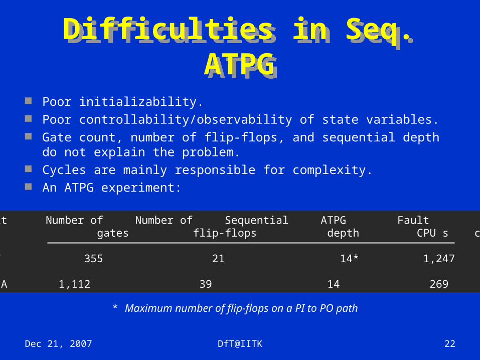
Difficulties in Seq. ATPGDifficulties in Seq. ATPG
Poor initializability. Poor controllability/observability of state variables. Gate count, number of flip-flops, and sequential depth do
not explain the problem. Cycles are mainly responsible for complexity. An ATPG experiment:
Circuit Number of Number of Sequential ATPG Fault gates flip-flops depth CPU s coverage
TLC 355 21 14* 1,247 89.01%
Chip A 1,112 39 14 269 98.80%
* Maximum number of flip-flops on a PI to PO path
Dec 21, 2007 DfT@IITK 23
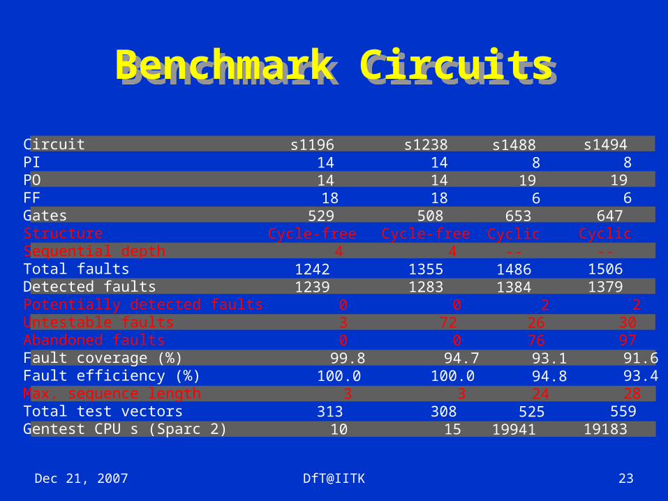
Benchmark CircuitsBenchmark Circuits
CircuitPIPOFFGatesStructureSequential depthTotal faultsDetected faultsPotentially detected faultsUntestable faultsAbandoned faultsFault coverage (%)Fault efficiency (%)Max. sequence lengthTotal test vectorsGentest CPU s (Sparc 2)
s1196 14 14 18 529
Cycle-free 412421239 0 3 0
99.8 100.0
3 313 10
s1238 14 14 18 508
Cycle-free 413551283 0 72 0
94.7 100.0
3 308 15
s1488 8 19 6 653
Cyclic--
14861384 2 26 76
93.1 94.8
24 52519941
s1494 8 19 6 647
Cyclic--
15061379 2 30 97
91.6 93.4
28 55919183
Dec 21, 2007 DfT@IITK 24
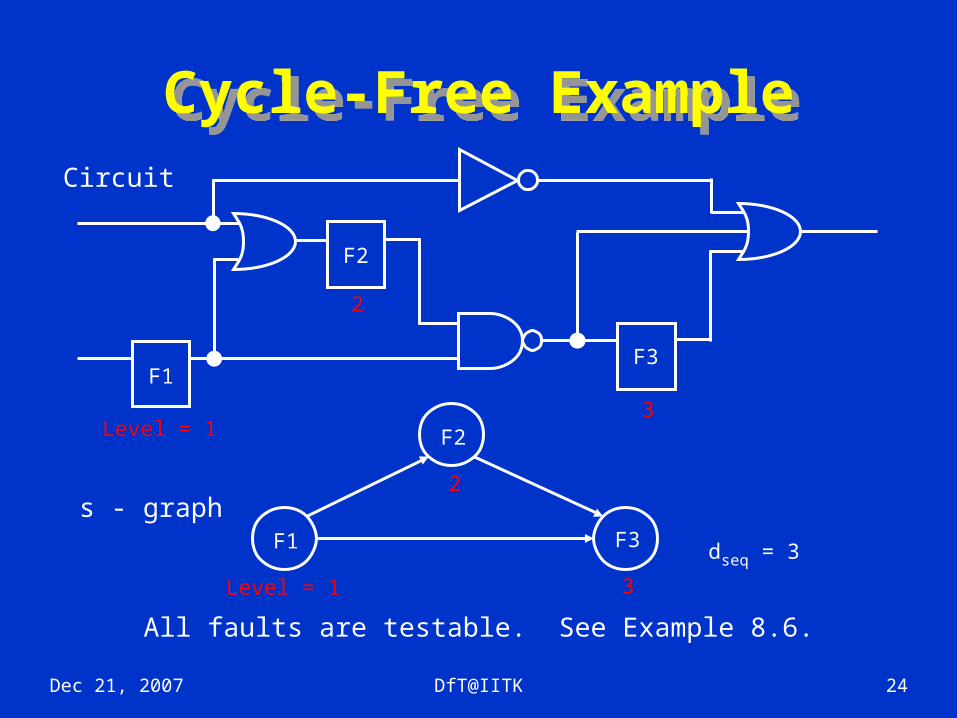
Cycle-Free ExampleCycle-Free Example
F1
F2
F3
Level = 1
2
F1
F2
F3
Level = 1
2
3
3
dseq = 3
s - graph
Circuit
All faults are testable. See Example 8.6.
Dec 21, 2007 DfT@IITK 25
Relevant ResultsRelevant Results
Theorem 8.1: A cycle-free circuit is always initializable. It is also initializable in the presence of any non-flip-flop fault.
Theorem 8.2: Any non-flip-flop fault in a cycle-free circuit can be detected by at most dseq + 1 vectors.
ATPG complexity: To determine that a fault is untestable in a cyclic circuit, an ATPG program using nine-valued logic may have to analyze 9Nff time-frames, where Nff is the number of flip-flops in the circuit.
Dec 21, 2007 DfT@IITK 26
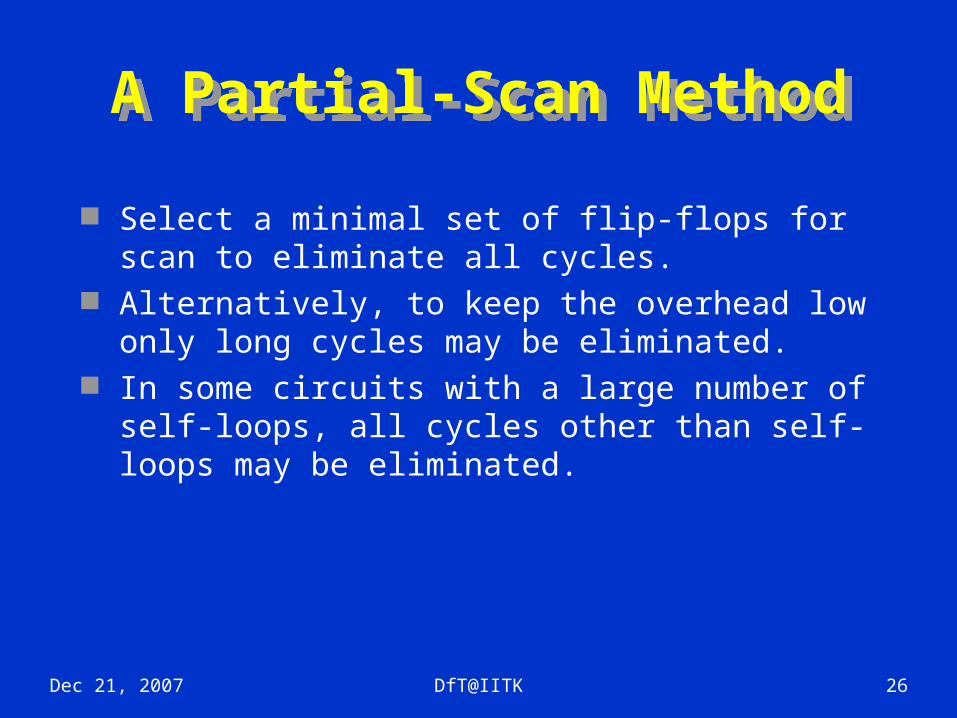
A Partial-Scan MethodA Partial-Scan Method
Select a minimal set of flip-flops for scan to eliminate all cycles.
Alternatively, to keep the overhead low only long cycles may be eliminated.
In some circuits with a large number of self-loops, all cycles other than self-loops may be eliminated.
Dec 21, 2007 DfT@IITK 27
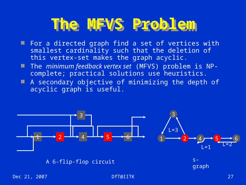
The MFVS ProblemThe MFVS Problem For a directed graph find a set of vertices with smallest
cardinality such that the deletion of this vertex-set makes the graph acyclic.
The minimum feedback vertex set (MFVS) problem is NP-complete; practical solutions use heuristics.
A secondary objective of minimizing the depth of acyclic graph is useful.
1 2
3
4 5 6L=3
1 2
3
4 5 6L=2L=1
s-graphA 6-flip-flop circuit
Dec 21, 2007 DfT@IITK 28
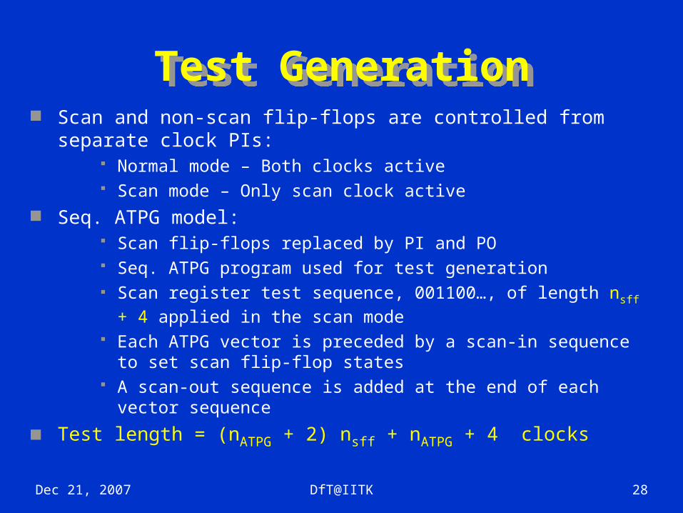
Test GenerationTest Generation Scan and non-scan flip-flops are controlled from separate
clock PIs: Normal mode – Both clocks active Scan mode – Only scan clock active
Seq. ATPG model: Scan flip-flops replaced by PI and PO Seq. ATPG program used for test generation Scan register test sequence, 001100…, of length nsff + 4
applied in the scan mode Each ATPG vector is preceded by a scan-in sequence to set
scan flip-flop states A scan-out sequence is added at the end of each vector
sequence
Test length = (nATPG + 2) nsff + nATPG + 4 clocks
Dec 21, 2007 DfT@IITK 29
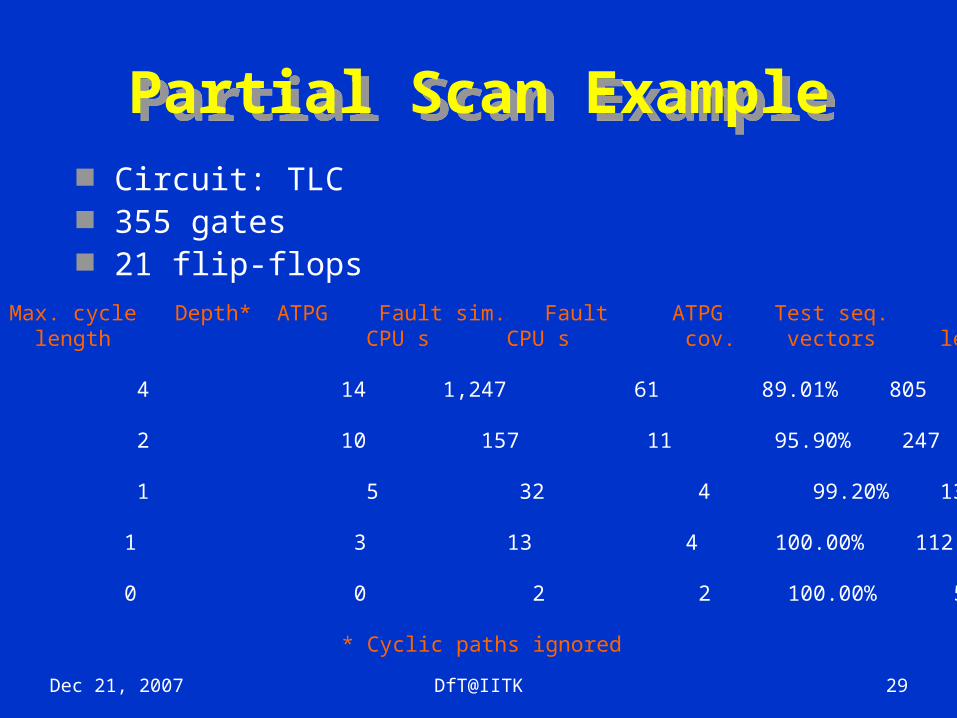
Partial Scan ExamplePartial Scan Example Circuit: TLC 355 gates 21 flip-flops Scan Max. cycle Depth* ATPG Fault sim. Fault ATPG Test seq.flip-flops length CPU s CPU s cov. vectors length
0 4 14 1,247 61 89.01% 805 805
4 2 10 157 11 95.90% 247 1,249
9 1 5 32 4 99.20% 136 1,382
10 1 3 13 4 100.00% 112 1,256
21 0 0 2 2 100.00% 52 1,190
* Cyclic paths ignored
Dec 21, 2007 DfT@IITK 30
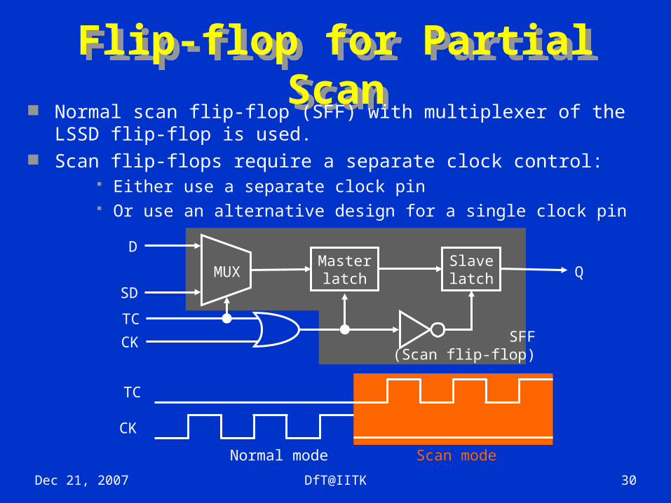
Flip-flop for Partial Scan
Flip-flop for Partial Scan
Normal scan flip-flop (SFF) with multiplexer of the LSSD flip-flop is used.
Scan flip-flops require a separate clock control: Either use a separate clock pin Or use an alternative design for a single clock pin
Masterlatch
Slavelatch
D
SD
TC
CK
MUX
SFF(Scan flip-flop)
Q
TC
CK
Normal mode Scan mode
Dec 21, 2007 DfT@IITK 31
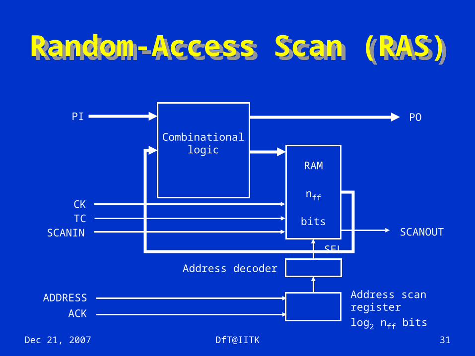
Random-Access Scan (RAS)
Random-Access Scan (RAS)
POPI
Combinationallogic
RAM
nff
bitsSCANOUTSCANIN
CKTC
ADDRESS
ACK
Address scanregisterlog2 nff bits
Address decoder
SEL
Dec 21, 2007 DfT@IITK 32
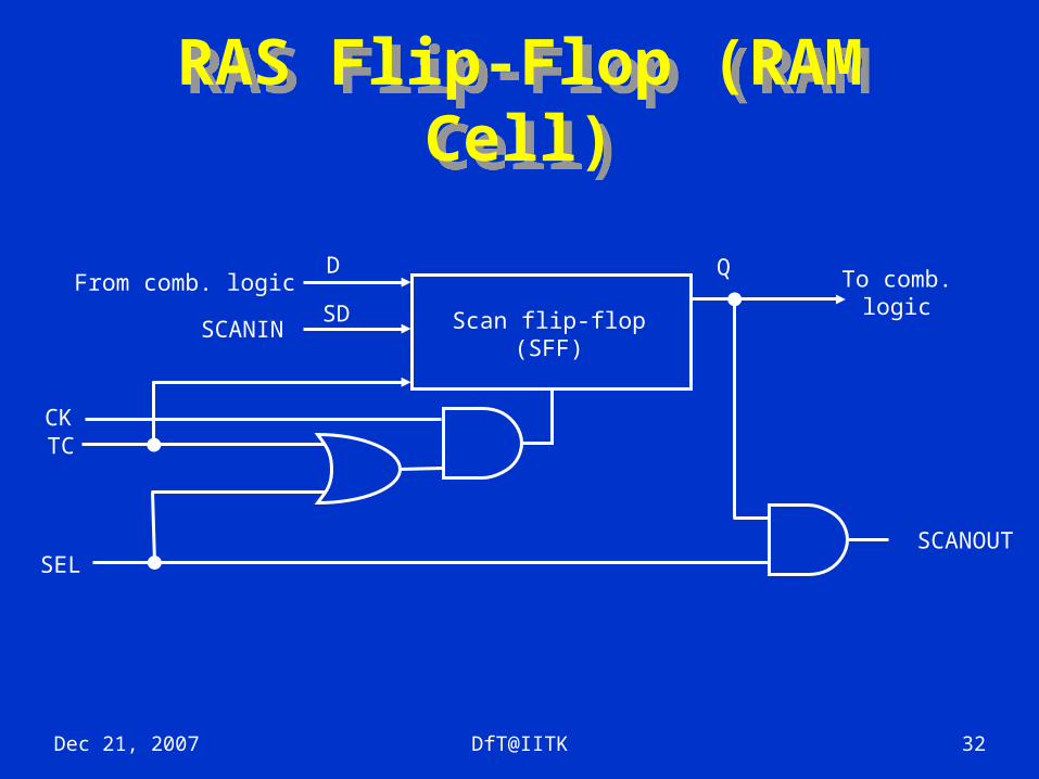
RAS Flip-Flop (RAM Cell)
RAS Flip-Flop (RAM Cell)
Scan flip-flop(SFF)
Q To comb.logic
D
SDFrom comb. logic
SCANIN
TCCK
SELSCANOUT
Dec 21, 2007 DfT@IITK 33
RAS ApplicationsRAS Applications
Logic test: Reduced test length Reduced scan power
Delay test: Easy to generate single-input-change (SIC) delay tests.
Advantage: RAS may be suitable for certain architecture, e.g., where memory is implemented as a RAM block.
Disadvantages: Not suitable for random logic architecture High overhead – gates added to SFF, address decoder,
address register, extra pins and routing
Dec 21, 2007 DfT@IITK 34
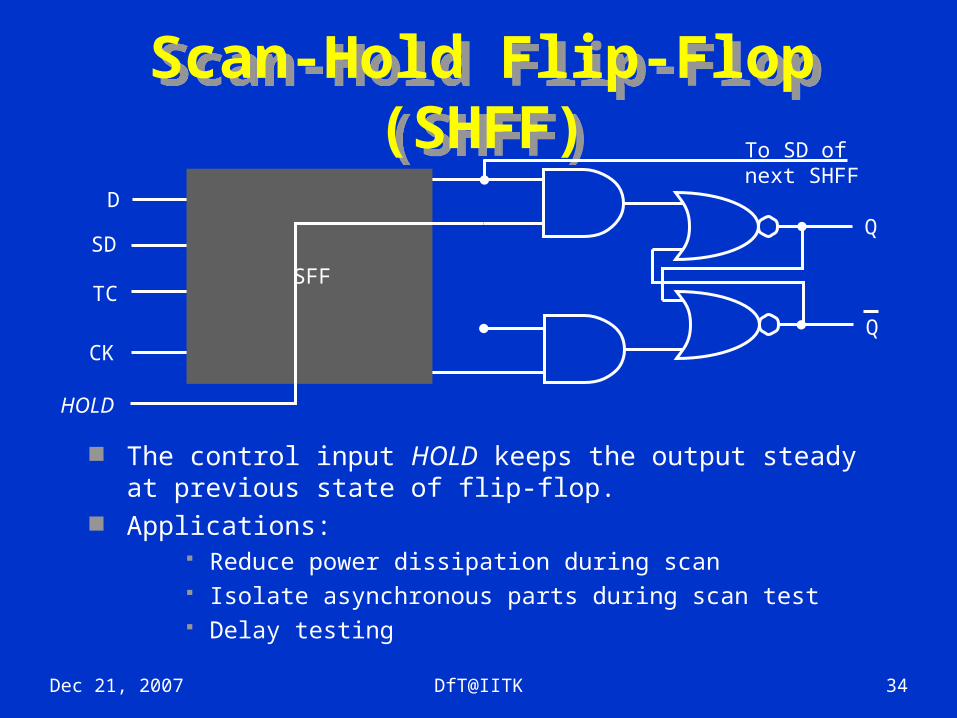
Scan-Hold Flip-Flop (SHFF)
Scan-Hold Flip-Flop (SHFF)
The control input HOLD keeps the output steady at previous state of flip-flop.
Applications: Reduce power dissipation during scan Isolate asynchronous parts during scan test Delay testing
SFF
D
SD
TC
CK
HOLD
Q
Q
To SD ofnext SHFF
Dec 21, 2007 DfT@IITK 35
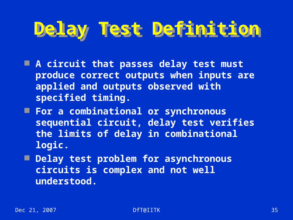
Delay Test DefinitionDelay Test Definition
A circuit that passes delay test must produce correct outputs when inputs are applied and outputs observed with specified timing.
For a combinational or synchronous sequential circuit, delay test verifies the limits of delay in combinational logic.
Delay test problem for asynchronous circuits is complex and not well understood.
Dec 21, 2007 DfT@IITK 36
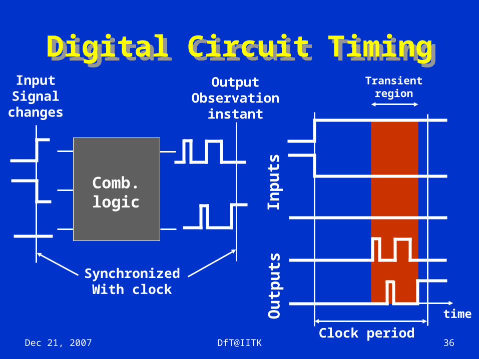
Digital Circuit TimingDigital Circuit Timing
Inp
uts
Ou
tpu
ts
time
Transientregion
Clock period
Comb.logic
OutputObservation
instant
InputSignal
changes
SynchronizedWith clock
Dec 21, 2007 DfT@IITK 37
Circuit DelaysCircuit Delays Switching or inertial delay is the interval between input change
and output change of a gate: Depends on input capacitance, device (transistor)
characteristics and output capacitance of gate. Also depends on input rise or fall times and states of other
inputs (second-order effects). Approximation: fixed rise and fall delays (or min-max delay
range, or single fixed delay) for gate output. Propagation or interconnect delay is the time a transition
takes to travel between gates: Depends on transmission line effects (distributed R, L, C
parameters, length and loading) of routing paths. Approximation: modeled as lumped delays for gate inputs.
See Section 5.3.5 for timing models.
Dec 21, 2007 DfT@IITK 38
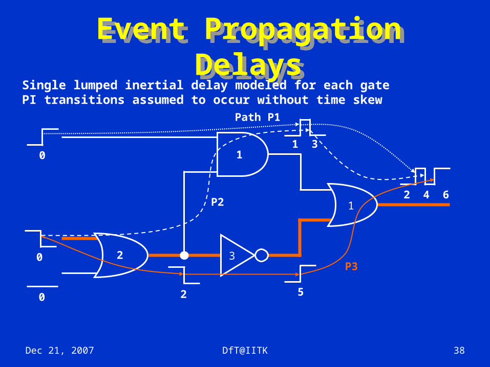
Event Propagation Delays
Event Propagation Delays
2 4 61
1 3
5
3
10
0
0
2
2
Path P1
P2
P3
Single lumped inertial delay modeled for each gatePI transitions assumed to occur without time skew
Dec 21, 2007 DfT@IITK 39
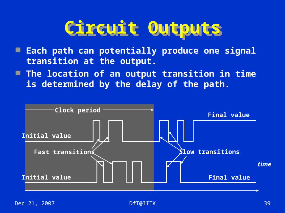
Circuit OutputsCircuit Outputs Each path can potentially produce one signal
transition at the output. The location of an output transition in time is
determined by the delay of the path.
Initial value
Initial value
Final value
Final value
Clock period
Fast transitions Slow transitions
time
Dec 21, 2007 DfT@IITK 40
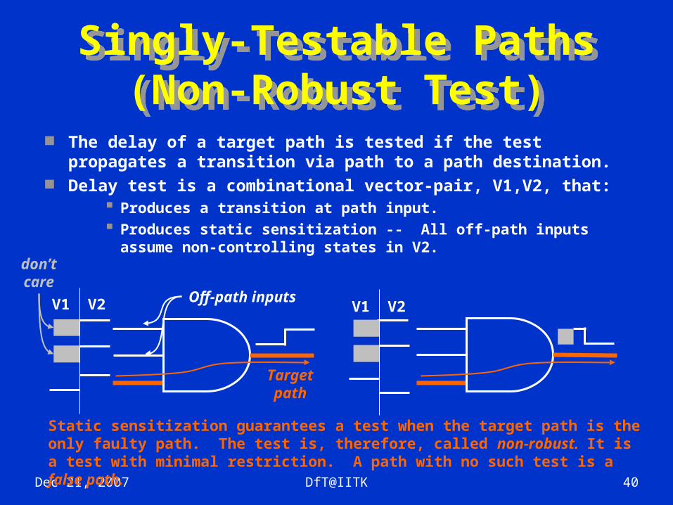
Singly-Testable Paths(Non-Robust Test)
Singly-Testable Paths(Non-Robust Test)
The delay of a target path is tested if the test propagates a transition via path to a path destination.
Delay test is a combinational vector-pair, V1,V2, that: Produces a transition at path input. Produces static sensitization -- All off-path inputs assume
non-controlling states in V2.
V1 V2 V1 V2
Static sensitization guarantees a test when the target path is the only faulty path. The test is, therefore, called non-robust. It is a test with minimal restriction. A path with no such test is a false path.
Targetpath
Off-path inputs
don’tcare
Dec 21, 2007 DfT@IITK 41
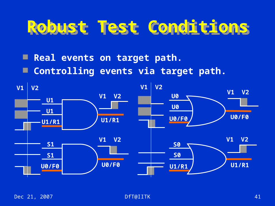
Robust Test ConditionsRobust Test Conditions
Real events on target path. Controlling events via target path.
V1 V2 V1 V2
V1 V2
V1 V2
V1 V2
V1 V2
U1
U1
U1/R1
S1
U0/F0
S1
U0
U0
U0/F0
U1/R1
U1/R1
U1/R1U0/F0
U0/F0
S0
S0
Dec 21, 2007 DfT@IITK 42
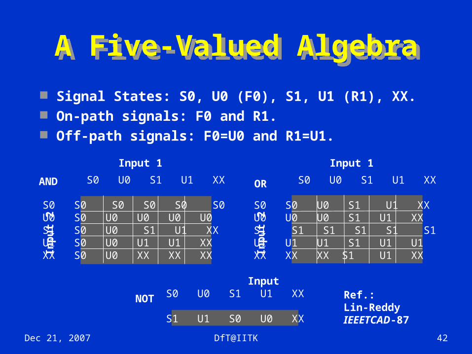
A Five-Valued AlgebraA Five-Valued Algebra
Signal States: S0, U0 (F0), S1, U1 (R1), XX. On-path signals: F0 and R1. Off-path signals: F0=U0 and R1=U1.
S0 U0 S1 U1 XX
S0 S0 S0 S0 S0 S0U0 S0 U0 U0 U0 U0S1 S0 U0 S1 U1 XXU1 S0 U0 U1 U1 XXXX S0 U0 XX XX XX
Input 1
Inp
ut
2
S0 U0 S1 U1 XX
S0 S0 U0 S1 U1 XXU0 U0 U0 S1 U1 XXS1 S1 S1 S1 S1 S1U1 U1 U1 S1 U1 U1XX XX XX S1 U1 XX
Input 1
Inp
ut
2
InputS0 U0 S1 U1 XX
S1 U1 S0 U0 XX
AND OR
NOT Ref.:Lin-ReddyIEEETCAD-87
Dec 21, 2007 DfT@IITK 43
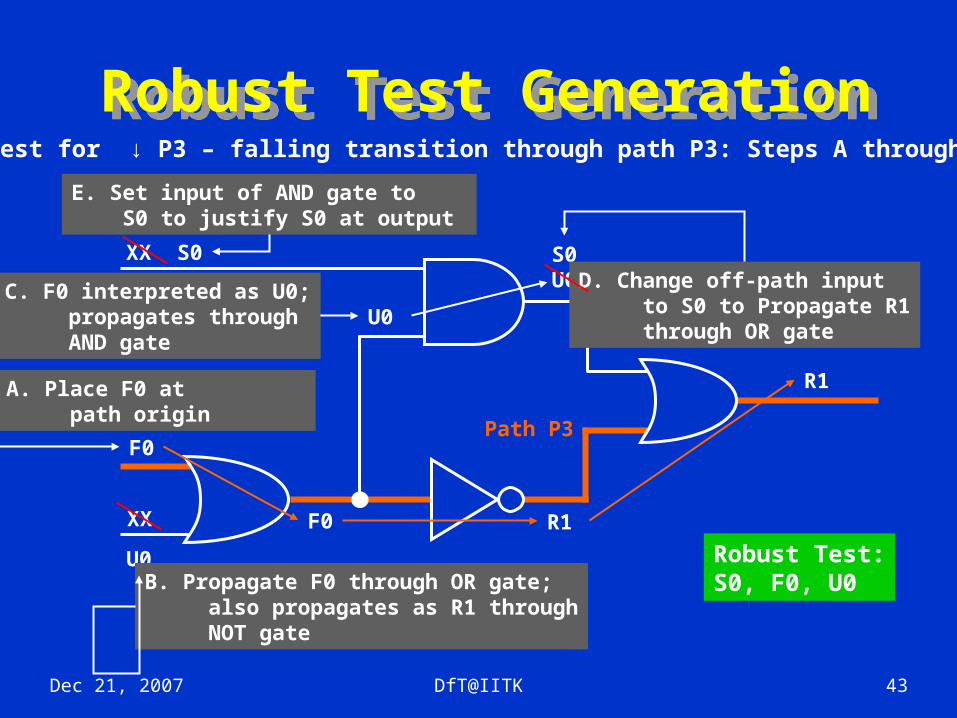
Robust Test GenerationRobust Test Generation
R1
S0U0
R1
XX S0
U0
F0
U0
Path P3
Test for ↓ P3 – falling transition through path P3: Steps A through E
F0
XX
A. Place F0 at path origin
B. Propagate F0 through OR gate; also propagates as R1 through NOT gate
C. F0 interpreted as U0; propagates through AND gate
D. Change off-path input to S0 to Propagate R1 through OR gate
E. Set input of AND gate to S0 to justify S0 at output
Robust Test:S0, F0, U0