Embed Size (px)
Citation preview

DECchip 21064Evaluation BoardUser’s GuideOrder Number: EC–N0351–72
Revision/Update Information: This is a revised document.
Digital Equipment CorporationMaynard, Massachusetts

First edition, May 1993Second edition, June 1993Third edition, September 1993
While Digital believes the information included in this publication is correct as of the date ofpublication, it is subject to change without notice.
Digital Equipment Corporation makes no representations that the use of its products in themanner described in this publication will not infringe on existing or future patent rights, nor dothe descriptions contained in this publication imply the granting of licenses to make, use, or sellequipment or software in accordance with the description.
© Digital Equipment Corporation 1993.Printed in U.S.A.
Alpha AXP, AXP, DEC, DECchip, Digital, ThinWire, the AXP logo, and the DIGITAL logo aretrademarks of Digital Equipment Corporation.
ABEL is a trademark of Data I/O Corporation.Viewlogic EDA is a trademark of Viewlogic Systems, Inc.SC486 is a trademark of VLSI Technology, Inc.AMD Am79C960 PCnet-ISA is a trademark of Advanced Micro Devices.

Contents
Preface . . . . . . . . . . . . . . . . . . . . . . . . . . . . . . . . . . . . . . . . . . . . . . . . . . . . . vii
Document Conventions . . . . . . . . . . . . . . . . . . . . . . . . . . . . . . . . . . . . . . ix
1 Introduction to the EB64
1.1 Components . . . . . . . . . . . . . . . . . . . . . . . . . . . . . . . . . . . . . . . . . 1–11.2 Uses . . . . . . . . . . . . . . . . . . . . . . . . . . . . . . . . . . . . . . . . . . . . . . . 1–31.3 Features . . . . . . . . . . . . . . . . . . . . . . . . . . . . . . . . . . . . . . . . . . . . 1–41.3.1 Memory Subsystem . . . . . . . . . . . . . . . . . . . . . . . . . . . . . . . . 1–41.3.2 Bcache Subsystem . . . . . . . . . . . . . . . . . . . . . . . . . . . . . . . . . 1–41.3.3 ISA Interface . . . . . . . . . . . . . . . . . . . . . . . . . . . . . . . . . . . . . 1–41.3.4 Slow-Speed Peripheral Device Interface . . . . . . . . . . . . . . . . . 1–51.3.5 Ethernet Port . . . . . . . . . . . . . . . . . . . . . . . . . . . . . . . . . . . . . 1–51.3.6 Debug ROM . . . . . . . . . . . . . . . . . . . . . . . . . . . . . . . . . . . . . . 1–51.3.7 Serial ROM . . . . . . . . . . . . . . . . . . . . . . . . . . . . . . . . . . . . . . 1–51.3.8 Expansion Interface . . . . . . . . . . . . . . . . . . . . . . . . . . . . . . . . 1–5
2 System Configuration and Connections
3 Functional Description
3.1 Address Space . . . . . . . . . . . . . . . . . . . . . . . . . . . . . . . . . . . . . . . 3–13.1.1 Address Bit Description . . . . . . . . . . . . . . . . . . . . . . . . . . . . . 3–13.1.2 Main Memory Address Space . . . . . . . . . . . . . . . . . . . . . . . . . 3–23.1.2.1 Main Memory, Bcacheable . . . . . . . . . . . . . . . . . . . . . . . . 3–23.1.2.2 Main Memory, Not Bcacheable . . . . . . . . . . . . . . . . . . . . . 3–33.1.2.3 Main Memory, Not Bcacheable or Data cacheable . . . . . . 3–4
iii

3.1.3 I/O Address Space . . . . . . . . . . . . . . . . . . . . . . . . . . . . . . . . . 3–53.1.3.1 I/O Address Space Mapping . . . . . . . . . . . . . . . . . . . . . . . 3–53.1.3.2 I/O Byte Enable and Transfer Length . . . . . . . . . . . . . . . 3–63.1.3.3 I/O Space, Debug ROM, and System Register . . . . . . . . . 3–63.1.3.4 I/O Space, SC486 and Interrupt Acknowledge . . . . . . . . . 3–73.1.3.5 I/O Space, Expansion Connector . . . . . . . . . . . . . . . . . . . 3–73.2 Memory Subsystem . . . . . . . . . . . . . . . . . . . . . . . . . . . . . . . . . . . 3–83.2.1 Main Memory Subsystem . . . . . . . . . . . . . . . . . . . . . . . . . . . . 3–83.2.1.1 Row and Column Addressing . . . . . . . . . . . . . . . . . . . . . . 3–113.2.1.2 Column 0 . . . . . . . . . . . . . . . . . . . . . . . . . . . . . . . . . . . . . 3–113.2.1.3 Address Bits 18 and 17 . . . . . . . . . . . . . . . . . . . . . . . . . . 3–123.2.1.4 DRAM Address Multiplexing . . . . . . . . . . . . . . . . . . . . . . 3–123.2.2 Bcache Subsystem . . . . . . . . . . . . . . . . . . . . . . . . . . . . . . . . . 3–143.2.2.1 Tag Address Bits <33:32> . . . . . . . . . . . . . . . . . . . . . . . . 3–163.2.3 Memory/Bcache Cycles . . . . . . . . . . . . . . . . . . . . . . . . . . . . . . 3–173.2.3.1 Hexaword DRAM Read (READ_BLOCK External
Access) . . . . . . . . . . . . . . . . . . . . . . . . . . . . . . . . . . . . . . . 3–173.2.3.2 Hexaword DRAM Write (WRITE_BLOCK External
Access) . . . . . . . . . . . . . . . . . . . . . . . . . . . . . . . . . . . . . . . 3–183.2.3.3 Victim Write . . . . . . . . . . . . . . . . . . . . . . . . . . . . . . . . . . . 3–183.2.3.4 Load Locked (LDxL External Access) . . . . . . . . . . . . . . . . 3–183.2.3.5 Store Conditional (STxC External Access) . . . . . . . . . . . . 3–193.2.3.6 Direct Memory Access . . . . . . . . . . . . . . . . . . . . . . . . . . . 3–193.2.3.7 Refresh . . . . . . . . . . . . . . . . . . . . . . . . . . . . . . . . . . . . . . . 3–203.3 I/O Subsystem . . . . . . . . . . . . . . . . . . . . . . . . . . . . . . . . . . . . . . . 3–203.3.1 I/O Devices . . . . . . . . . . . . . . . . . . . . . . . . . . . . . . . . . . . . . . . 3–203.3.1.1 System Register . . . . . . . . . . . . . . . . . . . . . . . . . . . . . . . . 3–203.3.1.2 Debug ROM . . . . . . . . . . . . . . . . . . . . . . . . . . . . . . . . . . . 3–253.3.1.3 ISA Interface and Associated Peripheral Devices . . . . . . . 3–263.3.1.4 Slow Speed Peripheral Devices . . . . . . . . . . . . . . . . . . . . 3–263.3.1.5 Ethernet Link . . . . . . . . . . . . . . . . . . . . . . . . . . . . . . . . . 3–273.3.1.6 Interrupts . . . . . . . . . . . . . . . . . . . . . . . . . . . . . . . . . . . . 3–273.4 Power, Reset, and Initialization . . . . . . . . . . . . . . . . . . . . . . . . . . 3–283.4.1 Reset . . . . . . . . . . . . . . . . . . . . . . . . . . . . . . . . . . . . . . . . . . . 3–283.4.2 Initialization and SROM . . . . . . . . . . . . . . . . . . . . . . . . . . . . 3–283.5 System Clocks . . . . . . . . . . . . . . . . . . . . . . . . . . . . . . . . . . . . . . . 3–30
iv
4 Expansion Interface
4.1 Expansion Connector Signal Description . . . . . . . . . . . . . . . . . . . 4–14.2 21064 Expansion Interface . . . . . . . . . . . . . . . . . . . . . . . . . . . . . . 4–154.2.1 Data Path Width . . . . . . . . . . . . . . . . . . . . . . . . . . . . . . . . . . 4–164.2.2 Cache Coherency . . . . . . . . . . . . . . . . . . . . . . . . . . . . . . . . . . 4–164.2.3 Expansion Connector Clocks . . . . . . . . . . . . . . . . . . . . . . . . . 4–184.2.4 Programmed I/O Through the Expansion Connector . . . . . . . 4–194.2.5 DMA Through Expansion Connector . . . . . . . . . . . . . . . . . . . 4–244.2.6 DRAM Address 0 . . . . . . . . . . . . . . . . . . . . . . . . . . . . . . . . . . 4–254.3 System Bus Acquisition and Release Sequence . . . . . . . . . . . . . . 4–274.4 Expansion Connector Pin Lists . . . . . . . . . . . . . . . . . . . . . . . . . . 4–28
5 Power Requirements
A Technical Support, Ordering, and Associated Literature
A.1 Information and Technical Support . . . . . . . . . . . . . . . . . . . . . . . A–2A.2 Ordering DECchip Products . . . . . . . . . . . . . . . . . . . . . . . . . . . . . A–2A.3 Associated DECchip Literature . . . . . . . . . . . . . . . . . . . . . . . . . . A–2A.4 Associated Digital Literature . . . . . . . . . . . . . . . . . . . . . . . . . . . . A–4A.5 Associated Third-Party Literature . . . . . . . . . . . . . . . . . . . . . . . . A–5
Index
Examples
3–1 BIU_CTL Initialization Code Segment . . . . . . . . . . . . . . . . . . 3–16
Figures
1–1 Block Diagram . . . . . . . . . . . . . . . . . . . . . . . . . . . . . . . . . . . . 1–22–1 EB64 Board Jumpers and Connectors . . . . . . . . . . . . . . . . . . 2–23–1 Address Bit Definitions . . . . . . . . . . . . . . . . . . . . . . . . . . . . . 3–13–2 Address Path . . . . . . . . . . . . . . . . . . . . . . . . . . . . . . . . . . . . . 3–93–3 Data Path . . . . . . . . . . . . . . . . . . . . . . . . . . . . . . . . . . . . . . . 3–103–4 DRAM Address Multiplexer Definitions . . . . . . . . . . . . . . . . . 3–133–5 Bcache Tag and Index . . . . . . . . . . . . . . . . . . . . . . . . . . . . . . 3–143–6 System Register . . . . . . . . . . . . . . . . . . . . . . . . . . . . . . . . . . . 3–213–7 I/O Address Formation . . . . . . . . . . . . . . . . . . . . . . . . . . . . . . 3–22
v

3–8 SROM Serial Port Diagram . . . . . . . . . . . . . . . . . . . . . . . . . . 3–303–9 System Clock Timing . . . . . . . . . . . . . . . . . . . . . . . . . . . . . . . 3–313–10 Clock Distribution . . . . . . . . . . . . . . . . . . . . . . . . . . . . . . . . . 3–324–1 Signal Name Changes . . . . . . . . . . . . . . . . . . . . . . . . . . . . . . 4–144–2 Expansion Interface Signals . . . . . . . . . . . . . . . . . . . . . . . . . . 4–164–3 Expansion Connector Control Setup . . . . . . . . . . . . . . . . . . . . 4–184–4 Programmed I/O Through the Expansion Connector . . . . . . . 4–204–5 System Bus Acquisition and Release . . . . . . . . . . . . . . . . . . . 4–27
Tables
2–1 EB64 Board Jumpers and Connectors . . . . . . . . . . . . . . . . . . 2–33–1 Address Space Partitioning . . . . . . . . . . . . . . . . . . . . . . . . . . 3–23–2 Cached and Noncached Memory Quadrants . . . . . . . . . . . . . . 3–23–3 Transfer Length and Byte Enable Decode . . . . . . . . . . . . . . . 3–63–4 SC486 Zone Decode . . . . . . . . . . . . . . . . . . . . . . . . . . . . . . . . 3–73–5 Memory Size Selection . . . . . . . . . . . . . . . . . . . . . . . . . . . . . . 3–83–6 DRAM SIMM Row/Column Definition . . . . . . . . . . . . . . . . . . 3–113–7 Victim Write Demultiplexed Address Bits 18 and 17
Sources . . . . . . . . . . . . . . . . . . . . . . . . . . . . . . . . . . . . . . . . . . 3–123–8 RAS Decode for 2- and 8-MB DRAM SIMMs . . . . . . . . . . . . . 3–133–9 Bcache Size Selection . . . . . . . . . . . . . . . . . . . . . . . . . . . . . . . 3–153–10 EB64 System Register Bit Description . . . . . . . . . . . . . . . . . . 3–213–11 ISA IRQ Input Definitions . . . . . . . . . . . . . . . . . . . . . . . . . . . 3–274–1 Expansion Connector Signals . . . . . . . . . . . . . . . . . . . . . . . . . 4–24–2 Expansion Connector Pin List . . . . . . . . . . . . . . . . . . . . . . . . 4–284–3 Expansion Connector Pin List — buf_data<127:0> . . . . . . . . 4–334–4 Expansion Connector Pin List — io_addr<31:2> . . . . . . . . . . 4–344–5 Expansion Connector Pin List — Vdd and gnd . . . . . . . . . . . 4–345–1 Voltage/Amp . . . . . . . . . . . . . . . . . . . . . . . . . . . . . . . . . . . . . . 5–1
vi
Preface
This guide describes the DECchip 21064 Evaluation Board (also called theEB64), an evaluation and development module for computing systems based onthe DECchip 21064 microprocessor.
AudienceThis guide is written for system designers and others who use the EB64to design or evaluate computer systems based on the DECchip 21064microprocessor.
ScopeThis guide describes the features, configuration, functional operation, andexpansion interface of the EB64. Designing hardware to interface to theexpansion connector requires most of the same knowledge as a 21064 designand is not included in this guide. Additional information is available inthe EB64 schematics and programmable-logic source files, and also in theliterature listed in Appendix A. Additional technical support is available fromthe DECchip Information Line, also included in Appendix A.
ContentThis guide contains the following chapters and appendices:
• Chapter 1 is an overview of the EB64.
• Chapter 2 provides EB64 configuration information.
• Chapter 3 is a functional description of the EB64.
• Chapter 4 describes the EB64 expansion interface.
• Chapter 5 describes the EB64 power requirements.
• Appendix A lists technical support services and associated documentation.
vii


Document Conventions
Bit and Field Abbreviations
RO — Read Only
Bits and fields specified as RO can be read but not written.
RW — Read/Write
Bits and fields specified as RW can be read and written.
WO — Write Only
Bits and fields specified as WO can be written but not read.
Bit NotationMultiple bit fields are shown as extents (see Ranges and Extents, below).
CautionCautions indicate potential damage to equipment or data.
Data UnitsThe following data unit terminology, common within Digital, is used throughoutthis guide.
ix
Term Words Bytes Bits Other
Word 1 2 16
Longword 2 4 32
Quadword 4 8 64
Octaword 8 16 128 Single read fill; that is, the cache space thatcan be filled in a single read access. It takestwo read accesses to fill a backup cache line(see Hexaword).
Hexaword 16 32 256 Cache block, cache line. The space allocated toa single backup cache block.
NoteNotes indicate general information.
NumberingAll numbers are decimal or hexadecimal unless otherwise indicated. In casesof ambiguity, a subscript indicates the radix of nondecimal numbers. Forexample, 19 is decimal, but 1916 and 19A are hexadecimal.
Ranges and ExtentsRanges are specified by a pair of numbers separated by two periods ( .. ) andare inclusive. For example, a range of integers 0..4 includes the integers 0, 1,2, 3, and 4.
Extents are specified by a pair of numbers in angle brackets ( <> ) separatedby a colon ( : ) and are inclusive. For example, bits <7:3> specifies an extentincluding bits 7, 6, 5, 4, and 3.
Schematic ReferencesLogic schematics are included in the EB64 design package. In this guide,references to schematic pages are printed in italics. For example:
‘‘ . . . multiplexers (schematic page addr_mux.1).’’
x

Signal NamesSignal names in text are printed in boldface lowercase. Mixed-case anduppercase conventions sometimes used for signal names are not used in thisdocument. For example:
Used in this Guide Not Used in this Guide
cwmask7 cWMask7 CWMASK7
xi


1Introduction to the EB64
The DECchip 21064 Evaluation Board (also called EB64) is an evaluationand development module for computing systems based on the DECchip 21064microprocessor (also called 21064). It gives the user a single-board platformfor the design, integration, and analysis of supporting logic, subsystems,and software. The EB64 is the first reference design offered for a Digitalmicroprocessor that implements the Alpha AXP architecture. This chapteris an overview of the EB64, its uses, and its features. Figure 1–1 is a blockdiagram of the system.
Note: Design Concepts
System design concepts are discussed in the application note Designinga System with the DECchip 21064 Microprocessor. Memory and backupcache design concepts are discussed in the application note Designinga Memory/Cache Subsystem for the DECchip 21064 Microprocessor. Ifyou are not familiar with the 21064, you are encouraged to read bothapplication notes. Appendix A gives ordering information and listsother associated documentation.
1.1 ComponentsThe DECchip 21064 Evaluation Board includes:
• DECchip 21064 running at 150 MHz
• Dynamic RAM (DRAM) main memory subsystem of 4 to 64 Mbytes
• External backup cache (Bcache) subsystem comprising 512 Kbytes of 12 nsstatic RAMs (SRAMs). The Bcache is read- and write-allocate, write-back,with 32-byte blocks.
Introduction to the EB64 1–1

Figure 1–1 Block Diagram
WMO_EB64_001
ISA
SC486
FDC37C651
DMA Control
Serial PortsAm79C960
Ethernet Control
INT TimerRTC
CONTROL
MDlatch
Debug
DRAM
ROM
System
DECchip
ControlLogic
SYSREG
SystemControlSignals
adr
data
buf_data
buf_addr mem_addr
io_dataadr
buf_data
buf_data
Bcachetag
tagadr
ParityGenerator
ISA ControlKeyboardMouse
Floppy Control
ndx
io_addr
EXPANSIONCONNECTOR
21064
• Serial boot ROM (SROM)
• Two programmable ROMs (PROMs) for debug. One, called the ‘‘debugROM,’’ is preprogrammed by Digital’s applications support group; the otheris user-programmable.
• ISA (IEEE P996) interface and two ISA connectors
• Embedded serial ports, timers, and Ethernet interface
• Latches, buffers, glue logic, power regulators, oscillators, decouplingcapacitors, and so on, as needed to form a complete system
• 21064 cooling-fan sensor in reset/dcok circuitry
• Connector and logic to supply the 21064 signals for user hardware designand debug
• Database and user documentation
1–2 Introduction to the EB64

The full database, including schematics and source files, are supplied with theEB64. User documentation is also included. The database allows designerswith no previous Alpha AXP experience to successfully create a working AlphaAXP system with minimal help.
1.2 UsesThe EB64 has a wide range of uses. The following are a few examples.
System DevelopmentIn its released configuration, the EB64 can be used as the basis of a fullcomputing system for which the user must design and integrate the necessarysupporting logic. The EB64 works under worst-case voltage, temperature, andprocess conditions, and can serve as the core of a high-volume product withoutsignificant changes.
Software DevelopmentThe EB64 has remote debug capability and a software debug monitor forloading code into the system and performing other software debug functionssuch as memory read, memory write, and instruction breakpoint. Whencombined with a hardware interface, the debug monitor can be used to writeand debug software (for example, device drivers) for workstation and PC-typeproducts, as well as for embedded control products such as laser printers,communication engines (such as bridges and routers), and video products.
Memory and Bcache Subsystem EvaluationThe EB64 is a high-speed design and includes a full 128-bit data path forthe DRAM main memory and the Bcache. The 21064 runs at full speed (150MHz), with power regulation and cooling handled on the board. The EB64high-performance Bcache SRAM subsystem takes into account signal integrityissues.
The user can select Bcache size and DRAM access time. Such flexibilityallows users to change these characteristics and run performance benchmarksto determine the effect on actual programs. The available hardwareconfigurations can also be combined and tested with different coding techniquesto determine optimum system performance.
I/O Device DevelopmentThe EB64 is a hardware and software platform for developing I/O devices tointerface with the 21064. An expansion connector is provided to allow accessto a buffered version of the 21064 external interface.1 The buffered interface
1 The expansion connector comprises two 80-pin connectors (J10 and J11) and two100-pin connectors (J26 and J27).
Introduction to the EB64 1–3

provides sufficient similarity to allow interfaces designed for the EB64 to beeasily adapted for direct connection to the 21064.
The expansion interface has a 39.6 ns cycle time, the same speed (25 MHz)as the on-board memory and I/O subsystems. Designers can easily implementappropriate expansion interfaces using commodity programmable devices asneeded.
1.3 FeaturesSections 1.3.1 through 1.3.8 give a brief overview of the major features of theEB64 system.
1.3.1 Memory SubsystemThe main memory subsystem accommodates 4 to 64 megabytes of DRAM,using four commodity single in-line memory module (SIMM) cards. EachSIMM card is 36 bits wide: 32 data bits, one parity bit, and three unused bits.The possible memory sizes are:
4 MB8 MB
16 MB32 MB64 MB
The default memory subsystem is a high-speed, 128-bit (plus parity)configuration. It can also be configured to emulate a slower (or narrower,64-bit) memory subsystem. For more information, see Section 3.2.1.
1.3.2 Bcache SubsystemThe 512-Kbyte Bcache uses a combination of commodity 32K�8, 32K�9,and 16K�4 12-ns SRAMs for data, parity, tag address, and tag control. Thelargest Bcache size is 512 kilobytes, but extra tag address bits are includedto configure other Bcache sizes of 256 or 128 kilobytes. The 21064 can beprogrammed to test SRAMs having lower speeds. Section 3.2.2 gives a detaileddescription of the Bcache.
1.3.3 ISA InterfaceThe VLSI Technology SC486 chip (VL82C486 chip with its companionVL82C113A combination I/O chip) provides the following functions:
• ISA bus controller, including bus master
• Direct memory access (DMA) controller
• Interrupt controller
1–4 Introduction to the EB64

• Programmable and refresh timers
• Real-time clock
• Mouse
• Keyboard
The SC486 also drives the two ISA slots on the EB64 board.
1.3.4 Slow-Speed Peripheral Device InterfaceThe combo I/O chip is a Standard Microsystems Corporation FDC37C651 SuperI/O Floppy Disk Controller. It connects directly to the ISA bus on the EB64board. It supplies two serial ports and a floppy-disk controller.
1.3.5 Ethernet PortThe AMD Am79C960 PCnet-ISA chip provides an Ethernet link. The chip andits associated glue logic (transformers, level shifters, capacitors, and so on)are connected to the ISA bus on the EB64 board. Both 10BaseT and 10Base2interfaces are provided. See Section 3.3.1.5 for more information.
1.3.6 Debug ROMThe debug ROM is an industry-standard, 512-kilobyte or 1-megabyte jumperselectable) PROM that contains the debug monitor code. The debug monitorallows the design engineer to develop code on a host system and load thesoftware into the EB64 through the Ethernet port or SROM serial line.
A second PROM socket (jumper selectable) is provided on the board for auser-programmable device. For more information see Section 3.3.1.2.
1.3.7 Serial ROMThe 21064 uses an SROM for its initialization code. When reset is deasserted,the contents of the SROM are read into the 21064’s instruction cache. Thecode is then executed from the instruction cache. See Section 3.4.2 for moreinformation.
1.3.8 Expansion InterfaceThe EB64 board includes a high-speed, 21064 pin-bus expansion interface.This interface gives access to a buffered version of the microprocessor pinbus. It includes the handshake signals needed to perform reads and writesto memory and I/O. This on-board interface ignores the memory zone definedto give system control to an external interface plugged into the connectors.Chapter 4 provides a complete description of the expansion interface.
Introduction to the EB64 1–5


2System Configuration and Connections
The EB64 must be configured for the user’s environment. The configurationjumpers and connectors (or headers) for user-supplied power and peripheraldevices are shown in Figure 2–1 and described in Table 2–1.
After the evaluation board is configured, power can be applied, and the debugmonitor can be run. The debug monitor and its commands are describedin the DECchip 21064 Evaluation Board Debug Monitor User’s Guide. Forinformation about other software design tools, see the literature listed inAppendix A.
System Configuration and Connections 2–1

Figure 2–1 EB64 Board Jumpers and Connectors
WM
O_E
B64
_020
J13
LED
s
1
J5
J6
J22
1
J30
J8
J10
1
J26
J11
1
J27
J41
1
1
J2J3
J28
J17
1 J29
J7
1
1
J12
J23
J1
SID
E 1
2106
4
J16
1
1J1
4
J15
1
J18
J19
J20
J21
J25 1
1
J24
J9
1
1
PR
OM
0
PR
OM
1
2–2 System Configuration and Connections
Table 2–1 EB64 Board Jumpers and Connectors
Connector Pins Description
J1J9
84
Ethernet connector, twisted-pair (10BASE-T)Ethernet connector, ThinWire (10BASE-2)
Note: Ethernet LEDs
The four LEDs in Figure 2–1 are driven by the PCnet-ISA chip(Am79C960) and indicate the following:
LED0: LINK OKLED1: RCVLED2: RX POL OKLED3: XMIT
J2J3
66
Board power connector (gndpin1, gnd, –5 V, Vdd, Vdd, Vdd)Board power connector (p_dcokpin1, Vdd, +12 V, –12 V, gnd, gnd)
Note: Power Supply
Power for the EB64 is provided by a user-supplied, standard, PCpower supply. Digital does not provide this power supply. SeeSection 3.4 for more information.
J4 4 Speaker connector. The speaker should be connected to pins 1and 4.
J5 3 PROM0 or PROM1 jumper. See Section 3.3.1.2 for moreinformation.
To Select Set Jumper Pins
PROM0 1 to 2PROM1 2 to 3
J6 4 Combo chip (FDC37C651) precompensation and drive-typejumpers
Signal Jumper In Out
Precompensation 1 to 2 low highDrive type 3 to 4 low high
(continued on next page)
System Configuration and Connections 2–3

Table 2–1 (Cont.) EB64 Board Jumpers and Connectors
Connector Pins Description
J7J13
9898
ISA Slot 1 connectorISA Slot 0 connector
J8 6 SROM serial port connectorSee Section 1.3.7 for more information.
J9 See J1
J10J11J26J27
8080
100100
Expansion interface connector. See Chapter 4 for moreinformation.
J12J14
1010
Combo chip (FDC37C651) serial port 1Combo chip (FDC37C651) serial port 2
J13 See J7
J14 See J12
J15 4 Battery backup connector for time-of-year (TOY) clock
J16�
J23�22
System reset switch connectordcok reset switch connectorSee Section 3.4.1 for more information.
J17 3 21064 fan power and sensor connector.
Caution: Fan Sensor Required
The 21064 cooling fan must have a built-in sensor that drivesa signal if the air flow stops. The sensor is connected to J17.The fan supplied with the EB64 includes an air-flow sensor. SeeSection 3.4 for more information.
J18J19J20J21
70707070
DRAM0 SIMM connectorDRAM1 SIMM connectorDRAM2 SIMM connectorDRAM3 SIMM connector
All four SIMM connectors must be populated. See Section 3.2.1for more information.
�The reset switch is connected to J16 or J23.
(continued on next page)
2–4 System Configuration and Connections

Table 2–1 (Cont.) EB64 Board Jumpers and Connectors
Connector Pins Description
J22 3 PROM size jumper. See Section 3.3.1.2 for more information.
To Select Set Jumper Pins
512-KB PROM 1 to 21-MB PROM 2 to 3
J23 See J16
J24 12 Keyboard (bottom)/mouse (top) connector
J25 8 System configuration jumpersSee Section 3.3.1.1 for more information.
Signal Jumper: In Out Description
sys_config0 1 to 5 low high Boot SROM Mini-Debugger
sys_config1 2 to 6 low high 1-MB or 16-MB DRAMSIMMs
sys_config2 3 to 7 low high Boot an alternate imagesys_config3 4 to 8 low high Reserved
J26J27
See J10See J10
J28 34 Combo chip (FDC37C651) floppy-disk drive 0 and 1 connector
J29 2 Reserved for Digital use
(continued on next page)
System Configuration and Connections 2–5

Table 2–1 (Cont.) EB64 Board Jumpers and Connectors
Connector Pins Description
J30 8 Logic analyzer headerSee Section 3.3.1.1 for more information.
Signal Pin Signal Pin
sys_output0 1 gnd 5sys_output1 2 gnd 6sys_output2 3 gnd 7sys_output3 4 gnd 8
2–6 System Configuration and Connections

3Functional Description
This chapter describes the functional operation of the EB64, except for theexpansion interface, which is described in Chapter 4.
3.1 Address SpaceSections 3.1.1 through 3.1.3.2 describe EB64 address space partitioning.
3.1.1 Address Bit DescriptionThe 34-bit EB64 address space is partitioned into memory space and I/O space.As shown in Figure 3–1 and Table 3–1, address bit adr33 determines whichspace is being addressed. When adr33 = 0, memory space is addressed, andwhen adr33 = 1, I/O space is addressed. Address bits adr<32:30> furtherdivide memory and I/O space as shown in Table 3–1.
Figure 3–1 Address Bit Definitions
WMO_EB64_002
Byte Enable
Transfer Length
Zone Selection
1 = IO0 = Memory
9 8 7 6 5 4 0293033 32
0 0 0 0 0
Functional Description 3–1

Table 3–1 Address Space Partitioning
Address Bit33 32 31 30 Description
0 0 0 0 Main DRAM memory, Bcacheable0 1 0 0 Main DRAM memory, not Bcacheable, parity not checked�
0 1 1 0 Main DRAM memory, not Bcacheable or data cacheable, parity notchecked�
1 0 0 0 I/O space, debug ROM/system register1 0 0 1 I/O space, interrupt ACK1 0 1 0 I/O space, SC486 memory1 0 1 1 I/O space, SC486 I/O1 1 – – I/O Space, expansion connector
�Shadows Bcacheable space.
The address areas are described in Sections 3.1.2 and 3.1.3.5.
3.1.2 Main Memory Address SpaceAll addresses with adr33 = 0 address main memory (DRAM) space. Addressbits adr<32:30> further divide main memory space into the zones described inSections 3.1.2.1 through 3.1.2.3.
3.1.2.1 Main Memory, BcacheableThis is the normal local memory area (adr<33:30> = 0000), and this addressrange should be used for most programs. CPU adr<32:30> determine whethermain memory read or write accesses should go to the Bcache (see Table 3–2).The 21064 probes the Bcache for valid data and starts an external cycle only ifthere is a cache miss.
Table 3–2 Cached and Noncached Memory Quadrants
Quadrant adr<33:32> Cached/Noncached
1 00 Always cached2 01 Always noncached3 10 Always noncached4 11 Cached or noncached
3–2 Functional Description

Note: Cached Quadrants Set In BIU_CTL
The BC_PA_DIS field (<35:32>) in the 21064 bus interface unit control(BIU_CTL) internal processor register (IPR) is usually programmedsuch that only the first memory quadrant (adr<33:32> = 00) isBcached.
ReadsOn reads:
1. System logic places return data in the Bcache.
2. Data Bus Read Acknowledge (drack_h<2:0>) signals the 21064 to:
• Store the data in its data cache or instruction cache, according to thetype of read.
• Check the cache fill data for good 32-bit parity.
If the Bcache fill block is valid and dirty, a victim write cycle is performedbefore the new data is returned. (The victim write cycle is described inSection 3.2.3.3.)
WritesOn writes, data is written into the Bcache under control of the system logic. Ifthe current Bcache block is valid and dirty:
1. It is written back to memory.
2. The DRAM memory is read to fill the background data over which the newdata is to be written.
3. After the fill is complete, the new data is written into the Bcache.
4. The Bcache line is updated to be valid and dirty.
3.1.2.2 Main Memory, Not BcacheableThis memory space (adr<33:30> = 0100) shadows the Bcacheable memoryspace (Section 3.1.2.1) and differs as follows:
• The data cannot be in the Bcache.
• Read data parity is not checked.
In this space, the 21064 does not probe the Bcache on reads and writes (theSROM-resident reset code must set the proper quadrant for this to happen),but goes directly to the expansion interface. Victim writes are never done.Data bus read acknowledge (drack_h<2:0>) signals the 21064 to store thedata in its data cache or instruction cache, according to the type of read, and
Functional Description 3–3

fill data is returned to the 21064 without touching the Bcache. Writes bypassthe Bcache and go directly to DRAM.
Caution: Do Not Write and Read to Different Memory Space
Do not write data to an address in Bcacheable memory space and readthat same local DRAM location from space that is not Bcacheable. TheBcached write places the data into the write-back Bcache, where itstays until flushed out for some reason. When you try to read thatsame location from memory space that is not Bcacheable (adr32 = 1),the processor bypasses the Bcache and fetches data that may be stale.Because the read appears to be normal, the external control logic doesnot probe the Bcache for the information.
Caution: Do Not Read and Write to Different Memory Space
Do not read data from Bcacheable memory space and write that data tomemory space that is not Bcacheable. The read and write will work thefirst time, but the Bcache will contain stale data. A subsequent readof that data from Bcacheable memory space will hit in the Bcache, andthe wrong data will be returned to the CPU.
3.1.2.3 Main Memory, Not Bcacheable or Data cacheableThis address space (adr<33:30> = 0110) shadows the Bcacheable address space(Section 3.1.2.1). The 21064 and the system logic bypass the Bcache. Readsand writes are the same as they are for memory space that is not Bcacheable(Section 3.1.2.2), except that on reads, drack_h<2:0> signals the 21064 not toload the data into its internal data cache. The system logic can return a singleread fill in this address space. A single read fill (128 bytes) usually occurswhen the requested data is a byte or longword.
Caution: Not for Instruction Fetch
Instruction stream (Istream) reads to this address range do not work,because the 21064 does not load the data into its instruction cache.The processor will malfunction if this address range is used to fetchinstructions.
3–4 Functional Description

3.1.3 I/O Address SpaceAll addresses with adr33 = 1 address I/O space. Address bits adr<32:30>further divide I/O space into the zones described in Sections 3.1.3.3 through3.1.3.5.
3.1.3.1 I/O Address Space MappingAddress mapping between the 21064 address bus (adr<33:5>) and the I/Oaddress (io_addr<31:2>2) changes, depending on whether the 21064 or a DMAdevice is bus master. DMA devices on the EB64 are the SC486 and, potentially,circuitry connected to the expansion connector.
Bus Master is 21064When the 21064 is bus master, the address lines are mapped as follows:
sys_ioadr<31:23>adr<29:9>
) io_addr<31:23>) io_addr<22:2>
In addition to this mapping, byte enables io_be<3:0> are decoded fromadr<8:5> as described in Section 3.1.3.2 to facilitate byte addressing on the I/Obus. The technique of using address lines to decode byte information is knownas ‘‘sparse address mapping.’’
A consequence of sparse address mapping is that memory attached to theexpansion connector cannot be addressed as a contiguous block (because 21064adr<8:5> signals are not available). To compensate for this, byte enable ext_be<1:0> and transfer length ext_tl<1:0> signals are available on the expansionconnector. They correspond to buf_adr<8:7> and buf_adr<6:5> as follows:
buf_adr8buf_adr7buf_adr6buf_adr5
) ext_be1) ext_be0) ext_tl1) ext_tl0
Bus Master is DMA DeviceWhen a DMA device takes control of the io_addr bus and drives an addressinto the Bcache and DRAM array, the address is not shifted, and the addresslines are mapped as follows:
io_addr<25:5> ) adr<25:5>
2 From the system register. See Section 3.3.1.1
Functional Description 3–5

Lower address resolution than this is provided by sel_col2 and sel_col_a0,which allow individual 16-byte octawords to be addressed (behaving as adr4).Longword resolution is provided on writes by the appropriate Bcache writeenable (we) and DRAM CAS signals.
3.1.3.2 I/O Byte Enable and Transfer LengthTable 3–3 shows how address bits adr<8:5> are encoded. The transfer lengthfor commands directed at I/O space is selected according to adr<6:5>. The byteenables asserted for such transfers are determined according to adr<8:7>.
Table 3–3 Transfer Length and Byte Enable Decode
ByteEnableadr<8:7>
TransferLengthadr<6:5> Transfer Length BE# �
AddressAdder†
00 00 Byte access 1110 00016
01 00 Byte access 1101 08016
10 00 Byte access 1011 10016
11 00 Byte access 0111 18016
00 01 Word access 1100 02016
01 01 Word access 1001 0A010 01 Word access 0011 12016
11 01 Reserved – –
00 10 Tribyte access 1000 04016
01 10 Tribyte access 0001 0C01x 10 Reserved – –
10 11 Longword access 0000 06016
01 11 Reserved – –1x 11 Reserved – –
�Byte enable is asserted low (0).†Adding this hexadecimal value to the base address asserts the corresponding BE# code.
3.1.3.3 I/O Space, Debug ROM, and System RegisterThe debug ROM and system register share this address zone (adr<33:30> =1000).
3–6 Functional Description

ReadsOn read accesses, data bits <7:0> return the contents of the debug ROMlocation addressed by io_addr<21:2>. This address is translated fromadr<28:9>. The upper data bits come from the system register. The systemregister returns the same data for any ROM address that is accessed.
WritesOn write accesses to this address zone, the system register is written withthe data contained in the upper data bits defined for the system register (seeSection 3.3.1.1). The read and write locations of control bits <25:8> remain thesame; therefore, a routine can read the current value, change the required bits,and write it back without shifting the data around.
3.1.3.4 I/O Space, SC486 and Interrupt AcknowledgeAddress zones adr<33:30> = 1001, 1010, and 1011 all access the SC486 device,using the standard host handshake and control signals: ads#, rdy#, m/io#,d/c#, and w/r#. The interrupt acknowledge cycle is a read cycle. The SC486memory and I/O cycles can be read or write cycles. Table 3–4 shows the resultsof each zone access on the SC486 host bus interface.
Table 3–4 SC486 Zone Decode
adr<33:30>CommandType m/io# d/c# w/r# SC486 Transfer Type
1001 Read 0 0 0 interrupt acknowledge1010 Read 1 1 0 SC486 memory read1010 Write 1 1 1 SC486 memory write1011 Read 0 1 0 SC486 I/O read1011 Read 0 1 1 SC486 I/O read
3.1.3.5 I/O Space, Expansion ConnectorThis address zone (adr<33:30> = 11xx) is dedicated to the expansion interfaceconnector. The on-board decode logic does not recognize or act on addressesin this zone except for barrier instructions, which it will terminate with acycle acknowledge (cack<2:0>). User-supplied logic is expected to return theappropriate handshake signals. The expansion connector signals are describedin Chapter 4.
Caution: No External Logic
The system will hang if there is no external logic and an address inthis zone is accessed. There is no timeout.
Functional Description 3–7

3.2 Memory SubsystemSections 3.2.1 through 3.2.3.7 describe the DRAM main memory subsystem,Bcache subsystem, and memory cycles. Figure 3–2 shows the memory/Bcacheinterface address path and Figure 3–3 shows the data path.
3.2.1 Main Memory SubsystemThe main memory subsystem is a high-speed, 128-bit (plus parity)configuration with optional read-data wrapping (see the system register WrapRead bit in Section 3.3.1.1). The memory subsystem can also be configuredto emulate a slower (or narrower, 64-bit) memory subsystem by programmingread slip cycles in system register bits <20:19>.
The EB64 supports DRAM main memory sizes from 4 through 64 megabytes.Buffered CPU address bits adr<25:5> are delivered directly to the memorysubsystem. The data bus width is 128 bits. Each DRAM SIMM is 36 bitswide (32 data bits, one parity bit, and three unused bits), and provides parityprotection on each longword (four bytes). The memory is longword writable, sothat read/modify/write cycles are not required for hexaword (32-byte) transfersthat are not fully masked.
The EB64 accommodates several DRAM SIMM sizes in four industry-standardDRAM SIMM sockets (J18, J19, J20, and J21, Figure 2–1 and Table 2–1).To fill the 128-bit (plus parity) DRAM data path width, all four sockets mustbe populated. Memory size is specified in the system register as shown inTable 3–5.
Table 3–5 Memory Size Selection
SystemRegister<24:22>
DRAMSize
SIMMType Main Memory
000 1-MB 256K�36 4 MB
001 2-MB 512K�36 8 MB
010 4-MB 1MB�36 16 MB
011 8-MB 2MB�36 32 MB
100 16-MB 4MB�36 64 MB
3–8 Functional Description
Figure 3–2 Address Path
WM
O_E
B64
_003
tag<
>
D0
D1
A0
WE
D0
D1
A0
WE
dwse
lta
gctl
mat
ch
ras
cas
we
taga
dr_h
taga
dr
tagc
tl
tagc
tl_h
cpu_
tagc
tl_w
e
cpu_
tag_
oe
sys_
tag_
oe
wrt
_tag
ctl_
oe
2106
4
HO
LDA
CK
adr<
>
A = Bsy
s_da
ta_a
4
sel_
col
row
add
r
col a
ddr
mem
_add
r<>m
ux_a
dr
taga
dr h
itA = B
wrt
_tag
adr_
oe
<25:
19>
<29:
26>
hold
a
hold
io_a
ddr
mem
_ioa
dr_o
eho
ld_a
ck
buf_
adr
inde
x<>
hold
_ack
inde
x<>
<18:
5>
mem
_ioa
dr_o
eho
ld_a
ck
sel_
taga
drho
ld_a
ckdi
s(
)
to C
PU
to C
PU
creq
sysc
lkou
t
dwse
l
sys_
tagc
tl_w
e
sys_
data
_a4
sys_
taga
dr_w
e
creq
sysc
lkou
t
Exp
ansi
onC
onne
ctor
Sys
tem
Con
trol
Logi
c
Bca
che
Tag
Con
trol
DR
AM
SC
486
RO
M
Par
ityG
en
Sys
tem
Reg
iste
r
expe
cted
tagc
tl
Functional Description 3–9

Figure 3–3 Data Path
WM
O_E
B64
_004
128
128
MD
latc
h
mem
_wr_
par_
oe
mem
_wr_
clke
nm
em_w
r_oe
<3:0
>
mem
_rd_
clke
nm
em_r
d_oe
44
MD
latc
h
io_p
ar_o
e
128
4
ras
cas
we
sys_
data
_we<
3:0>
sys_
data
_oe
sys_
data
_a4
doe_
l
data
+ p
arity
sysc
lkou
t
creq
2106
4
DR
AM
Exp
ansi
onC
onne
ctor
Par
ityG
ener
ator
Sys
tem
Con
trol
Logi
c
sysc
lkou
t
creq
doe_
l
cpu_
data
_we<
3:0>
cpu_
data
_oe<
3:0>
cpu_
data
_a4
drac
k
buf_
par
buf_
data
4 128
8 32io
_dat
a <3
1:0>
io_d
ata
<7:0
>
SC
486
RO
M
0 D
reg_
wrt
_clk
rom
_oe
Sys
tem
Reg
iste
r
rom
_oe
D0
D1
A0
WE
Bca
che
Dat
a
3–10 Functional Description

3.2.1.1 Row and Column AddressingThe system logic multiplexes the DRAM SIMM addresses to present the rowand column addresses at the proper time. The address multiplex definitionsdo not change with SIMM size; SIMMs that do not have a particular inputaddress bit ignore the upper address lines. Table 3–6 shows the row andcolumn definitions.
Table 3–6 DRAM SIMM Row/Column Definition
DRAMAddress
DemultiplexedSystemAddress Used For DRAM SIMM Size
col<8:1>� adr<12:5> All
row<8:0> adr<21:13>† All
col9 adr22 4-, 8-, and 16-MB
row9 adr23 4-, 8-, and 16-MB
col10 adr24 16-MB only
row10 adr25 16-MB only
�See Section 3.2.1.2, below.†See Section 3.2.1.3, below.
3.2.1.2 Column 0Because the read and write data width between the 21064 and main memoryis 128 bits, two complete access cycles are required to transfer a full hexaword(32 bytes) of data. This transfer is performed using DRAM page-mode access,changing the least significant column address bit between the first and second128-bit transfer. The column 0 address is formed differently on reads andwrites.
• On writes, the column 0 address is always low (0) for the lower octaword(128-bit) transfer, and is then incremented to 1 to write the upper octaword.
• On reads, the column 0 address depends upon the system data wrappingmode. If read data wrapping is:
Functional Description 3–11

– Disabled, the column 0 address behaves as it does for a write (low, thenhigh).
– Enabled (system register bit 21 = 1), the column 0 address is set tothe value in cwmask1 for the first octaword (cwmask1 represents theinternal value of adr4). The column 0 address is then complementedfor the second octaword.
Caution: Setting Data Wrapping Mode
The same wrapping behavior must be set in the 21064 BIU_CTL IPR(SYS_WRAP bit) and in the EB64 system register (Wrap Read bit,Section 3.3.1.1).
3.2.1.3 Address Bits 18 and 17During victim write cycles, the source of demultiplexed address bits 18 and 17,which become dram_addr<5:4>, depends on Bcache size. As Table 3–7 shows,the source is either the 21064 (adr_h<18:17>) or the Bcache tag addressSRAMs (tagadr<18:17>).
Table 3–7 Victim Write Demultiplexed Address Bits 18 and 17 Sources
Bcache Size Demultiplexed 18 Demultiplexed 17
128 KB tagadr18 tagadr17
256 KB tagadr18 adr_h17
512 KB adr_h18 adr_h17
3.2.1.4 DRAM Address MultiplexingThe EB64 address-decode logic generates two row-address strobe (RAS) signals.With the 1-, 4-, or 16-MB SIMMs, a single RAS signal controls the entireSIMM. With 2-MB or 8-MB SIMMs, a second RAS signal is used to furtherdecode the accessed DRAMs. Figure 3–4 shows DRAM address multiplexingand Table 3–8 shows the decode definitions for each RAS.
3–12 Functional Description

Figure 3–4 DRAM Address Multiplexer Definitions
WMO_EB64_022
025 5 424 23 22 21 13 12
Row Address <8:0> Column Address <8:1>
Column Address 9Row Address 9
Column Address 10Row Address 10
18 17
RAS select for 8−Mbyte DRAM SIMM
RAS select for 2−Mbyte DRAM SIMM
Used for 16−Mbyte DRAM SIMMs
Used for 16−, 8−, 4−Mbyte DRAM SIMMs
source depends on Bcache size* Victim write demultiplexed address 18:17
Used for all DRAM SIMM sizes
*
Table 3–8 RAS Decode for 2- and 8-MB DRAM SIMMs
RAS Memory Type adr24 adr22
0 2-MB x 08-MB 0 x
1 2-MB x 18-MB 1 x
Functional Description 3–13
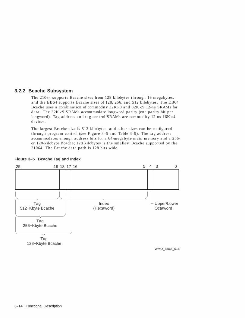
3.2.2 Bcache SubsystemThe 21064 supports Bcache sizes from 128 kilobytes through 16 megabytes,and the EB64 supports Bcache sizes of 128, 256, and 512 kilobytes. The EB64Bcache uses a combination of commodity 32K�8 and 32K�9 12-ns SRAMs fordata. The 32K�9 SRAMs accommodate longword parity (one parity bit perlongword). Tag address and tag control SRAMs are commodity 12-ns 16K�4devices.
The largest Bcache size is 512 kilobytes, and other sizes can be configuredthrough program control (see Figure 3–5 and Table 3–9). The tag addressaccommodates enough address bits for a 64-megabyte main memory and a 256-or 128-kilobyte Bcache; 128 kilobytes is the smallest Bcache supported by the21064. The Bcache data path is 128 bits wide.
Figure 3–5 Bcache Tag and Index
WMO_EB64_016
025 1819 1617 5 4 3
Tag512−Kbyte Bcache
Tag256−Kbyte Bcache
Tag128−Kbyte Bcache
Upper/LowerIndex(Hexaword) Octaword
3–14 Functional Description
Table 3–9 Bcache Size Selection
SystemRegister<18:17> Bcache Size Tag Address Bits
00 128 KB <25:17>01 256 KB <25:18>10 512 KB <25:19>11 Undefined
The physical EB64 Bcache is always 512 kilobytes. No physical changesare required to test a smaller Bcache. When a 128-kilobyte or 256-kilobyteBcache size is specified, part of the 512-kilobyte Bcache is ignored. On read-filloperations, the entire tag field is written (as if the 128-kilobyte Bcache size isspecified), but the tag address parity includes only the address bits appropriatefor the Bcache size selected. For example, when the 512-kilobyte Bcache isselected, tag address bits <18:17> are ignored.
Note: Setting Bcache Size
To configure the EB64 for a smaller Bcache size, the EB64 systemregister and the 21064 must be programmed for the smaller value. TheDECchip 21064 Microprocessor Hardware Reference Manual explainshow to program the CPU for Bcache size. The EB64 system register(Section 3.3.1.1) specifies a smaller Bcache size in the EB64 as shownin Table 3–9.
The EB64 uses 12 ns data and tag SRAMs, allowing the 21064 BIU_CTL IPR(BC_RD_SPD and BC_WR_SPD fields) to be programmed for 5/5 read/writecycle times. That is, each 128-bit access, including the tag probe, can beprogrammed for five CPU internal cycles (6.6 ns). It takes ten cycles to readan entire Bcache line — two 16-byte reads with the tag probe hidden underthe first octaword (16 bytes) read. A write to the Bcache consists of a five-cycletag probe and one or two Bcache write accesses, depending on which longwordsneed to be modified. The write pulse should be centered in each five-cycle writeaccess. The 21064 can be programmed to test SRAMs having slower speeds forperformance comparisons.
Example 3–1 is a code segment that can be used as a starting point whenprogramming the 21064 BIU_CTL IPR.
Functional Description 3–15

Example 3–1 BIU_CTL Initialization Code Segment
# biuCtl = 0x0E20006335# what bits value# ------- ------ -----# bc_en 0 1 Enable Bcache# ecc 1 0 Disable ECC# oe 2 1 output_enable, enabled# bc_fhit 3 0 disable Bcache force hits# bcRdSpd 7..4 4 5 cycle read# bcWrSpd 11..8 4 5 cycle write# unused 12 0# bcWeCtl 27..13 7 3 cycle write pulse; 2nd, 3rd, and 4th# cycles (000000000000111)# bc_size 30..28 010 Bcache size 512KB# bad_tp 31 0 Disable, force write bad tag cntl parity# bcPaDis 35..32 1110 Cache only 1st quad of physical address# bad_dp 36 0 Disable, force write bad ECC/parity# unused 63..37 0
lda r20, 0xE(r31) # biu_ctl[47:32] = 0xEsll r20, 32, r20 # Shift into positionldah r20, 0x2000+1(r20) # biu_ctl[31:16]=0x2001lda r20, 0xE445(r20) # biu_ctl[15:0]=0xE445mtpr r20, biuCtl # Write to biuCtl
Caution: Set BIU_CTL OE to Avoid Component Damage
The 21064 BIU_CTL IPR output enable bit (OE, bit 2) must be set onthe EB64 platform. If this bit is inadvertently cleared, the tag and dataSRAMs will be enabled during writes, resulting in damage.
3.2.2.1 Tag Address Bits <33:32>Tag address bit 33 is stored in the Bcache tag address SRAMs and is driven tothe 21064 tagadr_h<33:32> inputs for the tag compare. This allows a customdevice plugged into the expansion connector to have some of its data in theBcache (see Chapter 4) . This can be useful for a device such as a video framebuffer, which manipulates data at high speed before writing it out to framememory on the expansion connector.
Tag address bits 33 and 32 are either both zero or both one, and require onlya single bit (tagadr33) in the tag address SRAMs. For normal memory traffic,tagadr33 is zero, and memory operation is not affected. To address a deviceconnected to the expansion connector, adr<33:32> = 11, and that value isdriven into the Bcache tag address SRAMs when the Bcache is loaded. (The
3–16 Functional Description

shared [S] bit must be set.) Because parity is the same for tagadr<33:32> =00 or 11, parity generation does not change to support this feature.
The shared bit allows software for devices on the expansion connector to readand manipulate data at high speed, but prevents the data from being writtento (and deferred). If the shared bit is not set, the write-back Bcache saves thedata (until it is flushed out for some reason), which is not useful for a videoframe buffer. Tag address bit 33 also goes to the system-level tag comparelogic, so that expansion connector data is not aliased with normal memorydata.
Note: Set Cacheable Quadrants In BIU_CTL
When the system is used in this mode, the BC_PA_DIS field in the21064 BIU_CTL IPR should be programmed to set the lowest andhighest memory quadrants (adr<33:32> = 00 and 11) as cacheable.
3.2.3 Memory/Bcache CyclesThe EB64 memory control interface contains the state machine and glue logicneeded for turning 21064 bus signals into DRAM/Bcache cycles. The supportedcycles are described in Sections 3.2.3.1 through 3.2.3.6.
3.2.3.1 Hexaword DRAM Read (READ_BLOCK External Access)Cached and noncached hexaword DRAM reads are supported. The systemlogic returns the data to the 21064, and, if the data is in the cached area,simultaneously loads it into the Bcache.
The memory interface supports wrapped reads, where the requested octaword(16 bytes) is returned first. Nonwrapped reads always return the low octawordfirst, regardless of the address.
Caution: Setting Data Wrapping Mode
The same wrapping behavior must be set in the 21064 BIU_CTL IPR(SYS_WRAP bit) and in the EB64 system register (Wrap Read bit,Section 3.3.1.1).
Functional Description 3–17

3.2.3.2 Hexaword DRAM Write (WRITE_BLOCK External Access)Cached and noncached hexaword DRAM writes are supported. The 21064write data is accepted and loaded into memory on writes to a noncached areaor loaded into the Bcache on writes to the cached area. When the Bcache isthe final destination, a victim write is performed, if necessary, and the memoryblock is loaded into the Bcache, overwriting the modified longwords. (Thevictim write cycle is described in Section 3.2.3.3.)
3.2.3.3 Victim WriteA victim write cycle is generated by the system logic before a read or writecommand overwrites a Bcache block that is valid and dirty. The contents ofthe Bcache block are written to memory before the new data is loaded frommemory.
A victim write begins with a probe of the tag control bits, checking the valid(V) and dirty (D) bits on the Bcache block. If both are true, the Bcache block iswritten back to memory. If either is false, a victim write cycle does not beginand the read or write access proceeds normally.
3.2.3.4 Load Locked (LDxL External Access)The load locked cycle is similar to a READ_BLOCK access (Section 3.2.3.1).System logic first probes the Bcache for the requested data, because the 21064does not probe the Bcache on a LDxL command.
• If the data is in the Bcache, it is returned from there; otherwise, the datais returned from memory.
• If the data is returned from cacheable memory space, it is also loaded intothe Bcache.
In either case, the lock flag is unconditionally set. If a victim write isnecessary, it is performed before the read access.
Because the EB64 is expected to be used as a single-processor evaluationand development vehicle, lock contention is unlikely and the lock flag has noassociated address information. The lock is set on the load_locked instruction(LDxL command), and cleared by a store_conditional instruction (STxCcommand) or a DMA write (unconditional clear, not based on hit).
3–18 Functional Description

3.2.3.5 Store Conditional (STxC External Access)An STxC command on the 21064 external command bus generates this cycle.First, the lock flag is checked. If it is clear, the store_conditional instructionfails and a write is not performed. Command acknowledge (cack_h<2:0>)identifies the failed transaction.
If the lock flag is set, then a write command is performed. The Bcache ischecked to see if it contains the data, and one of the following occurs:
• If the data is in the Bcache, then the new data overwrites the data in theBcache and the block is marked dirty.
• If the data is not in the Bcache and the new data is noncacheable, then thenew data is written to a noncached memory area.
• If the data is not in the Bcache and the new data is cacheable, then theBcache is loaded from memory and is then overwritten with the new data.If required, a victim write (Section 3.2.3.3) is performed first.
The lock flag is cleared whether the transaction succeeds or fails.
3.2.3.6 Direct Memory AccessDirect memory access (DMA) cycles transfer data between an external bus andlocal DRAM or Bcache memory. The EB64 provides the ISA bus as the externalbus. Both DMA and master mode ISA transfers are possible. Because the ISAbus is only 16 data bits wide, each data transfer is limited to no more than twobytes (one word) per access. EB64 control logic provides the necessary Bcacheprobe and write data merge functions.
A DMA access is initiated when the SC486 senses an enabled request from anISA bus device. When it is idle, the EB64 control logic recognizes the DMArequest (hold) and responds with an acknowledge (hold_a). The acknowledgeis returned to the ISA device, and it then takes control of the bus and startsthe transfer. When the EB64 senses the transfer start, it probes the Bcache. Ifthe requested data word is currently valid in the Bcache and the transaction isa:
• Write, the EB64 modifies the data in the Bcache and sets the block dirty.It also invalidates the internal data cache.
• Read, the EB64 reads the data from the Bcache.
If the data is not valid in the Bcache, the transfer accesses main memory.
On write cycles, the current Bcache or DRAM data is read and saved, thenmerged with the new data from the SC486 according to the byte enable signals.The lock flag is cleared for DMA writes to either the Bcache or main memory.
Functional Description 3–19

The EB64 can read, write, and merge data from any longword (four bytes) inthe address space. It correctly updates the new longword parity on the mergedwrite data in the Bcache and main memory.
3.2.3.7 RefreshThe memory state machine performs memory refresh cycles according to atimer. A CAS-before-RAS refresh is performed on the entire DRAM array.
3.3 I/O SubsystemThe I/O subsystem includes the I/O state machine, glue logic, and thecomponents described in Section 3.3.1.
3.3.1 I/O DevicesThere are several input/output devices embedded in the EB64. The SC486,debug ROM, and system register share the same state machine. When thedebug ROM or system register are accessed, signal lba is asserted low toinhibit the SC486 from responding.3 This decision is based upon the addresszone, as defined in Section 3.1.
3.3.1.1 System RegisterThe EB64 has one system register. Its bits are defined in Figure 3–6 anddescribed in Table 3–10. The register is addressed as described in Table 3–1.The system register is a combination of a control register and the debug ROM.
WriteWhen the system register is written, register bits <25:8> are written withdata<25:8> (data mapping is 1:1), and the register low byte, <7:0>, is ignored.Register bits <29:26> are written to system output registers, where they canbe accessed with a logic analyzer connected to J30 (Figure 2–1 and Table 2–1).Bits <29:26> are not readable.
ReadWhen the system register is read, the bits return the following:
• <7:0> — The low byte returns the data from the debug ROM locationselected by the lower address bits, adr<28:9> (Figure 3–1). These addressbits translate to I/O address bits io_addr<21:2>.
• <25:8> — These bits return the control fields, irrespective of lower addressbits adr<28:9>. The control fields are written into the same data bitpositions from which they are read.
3 For more information about signal lba, see SC486 documentation.
3–20 Functional Description
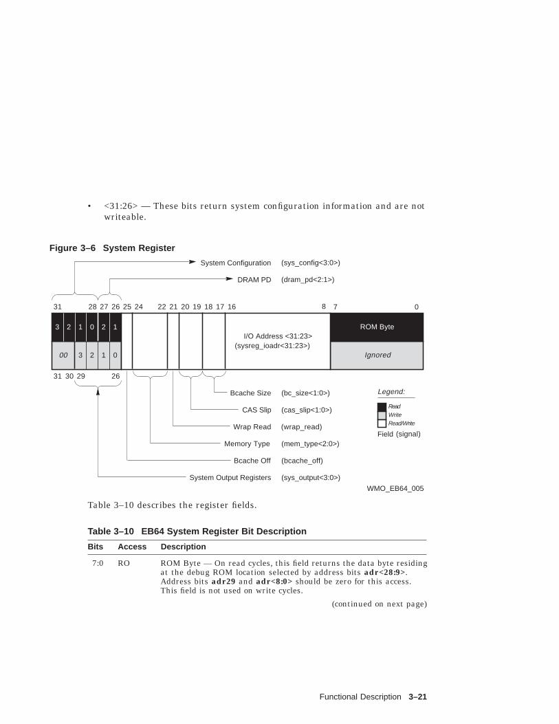
• <31:26> — These bits return system configuration information and are notwriteable.
Figure 3–6 System Register
WMO_EB64_005
8 7 019 18 17 1622 21 202425
ROM Byte
System Configuration
DRAM PD
26272831
Ignored
CAS Slip
Memory Type
Wrap Read
Bcache Size
Bcache Off
System Output Registers
2631 2930
3 2 1 0 2 1
3 2 1 000
ReadWrite
Legend:
Read/Write
(sysreg_ioadr<31:23>)
(sys_config<3:0>)
I/O Address <31:23>
(cas_slip<1:0>)
(mem_type<2:0>)
(wrap_read)
(bc_size<1:0>)
(bcache_off)
(sys_output<3:0>)
(dram_pd<2:1>)
Field (signal)
Table 3–10 describes the register fields.
Table 3–10 EB64 System Register Bit Description
Bits Access Description
7:0 RO ROM Byte — On read cycles, this field returns the data byte residingat the debug ROM location selected by address bits adr<28:9>.Address bits adr29 and adr<8:0> should be zero for this access.This field is not used on write cycles.
(continued on next page)
Functional Description 3–21

Table 3–10 (Cont.) EB64 System Register Bit Description
Bits Access Description
16:8 RW I/O Address <31:23> — This field defines address bits <31:23> in I/Ospace. It is concatenated with io_addr<22:2> to form the entire I/Oaddress. I/O address bits io_addr<22:2> are controlled by addressbits adr<29:9> from the processor. See Figure 3–7.
Figure 3–7 I/O Address Formation
WMO_EB64_025
8
8
7 0
0
17 16
ROM Byte
21
31
0 2 Byte Decode
29 9 4
00000
5
adr<8:5>
2231 23 2
ioadr<31:2>
adr<29:9>
sysreg_ioadr<31:23>
(continued on next page)
3–22 Functional Description

Table 3–10 (Cont.) EB64 System Register Bit Description
Bits Access Description
18:17 RW Bcache Size — This field determines the EB64 Bcache size selection,as follows:
18 17 Bcache Size
0 0 128 KB0 1 256 KB1 0 512 KB1 1 Undefined
Note: Setting Bcache Size
The Bcache size selected by this field must match the Bcache sizeselected in the BC_SIZE field in 21064 BIU_CTL IPR.
See Section 3.2.2 for more information on the Bcache subsystem.
20:19 RW CAS Slip — The memory subsystem is designed to run as fast aspossible using 70 ns commodity DRAM SIMMs and a 39.6 ns statemachine granularity. To emulate slower devices or narrower datapaths (translating to longer latency), slip cycles can be programmedinto the read cycles. There are two CAS accesses per read fill, andeach CAS is governed by the number of extra cycles in this field.This field programs the number of 39.6 ns slip cycles for each CASread access, as follows:
20 19 CAS Slip Cycles
0 0 00 1 11 0 21 1 3
(continued on next page)
Functional Description 3–23

Table 3–10 (Cont.) EB64 System Register Bit Description
Bits Access Description
21 RW Wrap Read — On read fill operations, the EB64 does two 16-byteDRAM reads to return a 32-byte hexaword. When this bit is clear,read data wrapping is disabled; that is, the low 16 bytes are alwaysreturned first, regardless of the request address. When this bit isset, read data wrapping is enabled and the requested 16 bytes arereturned first, according to address bit adr4 (translated to cwmask1during read). Write operations are not affected.
Caution: Setting Data Wrapping Mode
The 21064 BIU_CTL IPR (SYS_WRAP bit) must also be programmedfor this mode to work correctly.
24:22 RW Memory Type — The EB64 accommodates several DRAM SIMMsizes, allowing main memory size to be between 4 and 64 megabytes.This field selects the memory size as follows:
24 23 22 DRAM Size SIMM Type Main Memory
0 0 0 1-MB 256K�36 4 MB0 0 1 2-MB 512K�36 8 MB0 1 0 4-MB 1MB�36 16 MB0 1 1 8-MB 2MB�36 32 MB1 0 0 16-MB 4MB�36 64 MB
See Section 3.2.1 for more information on memory size selection andcontrol.
25 RW Bcache Off — When this bit is set, the system logic ignores theBcache. External system logic does not probe the Bcache, and allDMA transactions assume data is in DRAM memory.
Caution: Setting Bcache Off/On
The setting of this bit should correspond to the setting of the Bcacheenable bit (BC_EN, bit 0) in the 21064 BIU_CTL IPR.
27:26 RO DRAM PD<2:1> — During system register read accesses, thesebits reflect the DRAM SIMM configuration information PD<2:1>,which provides information about the size of the DRAMs. Becausethe 1-megabyte SIMM information aliases with the 16-megabyteinformation, a system configuration bit should be used with this field(sys_config1 — see bit 28, below).
(continued on next page)
3–24 Functional Description

Table 3–10 (Cont.) EB64 System Register Bit Description
Bits Access Description
31:28 RO System Configuration Jumpers <3:0> — During system registerread accesses, these bits reflect the state of the four EB64 boardconfiguration jumpers sys_config<3:0> (J25, Figure 2–1 andTable 2–1). The default configuration bit state is high: Eachconfiguration bit is pulled up on the EB64 board, and inserting ajumper pulls them down. The bits are defined as follows:
Signal J25 pins Description
sys_config0 1 to 5 Reserved.sys_config1 2 to 6 DRAM SIMM Size — This bit
completes the DRAM SIMM sizeinformation. Because the 1-MB and16-MB SIMMs are aliases, this bitindicates which of the two is installed.If the bit reads high (default), itindicates that 1-, 2-, 4-, or 8-MBDRAM SIMMs are installed. ThePD bits (<27:26>, above) identify thespecific size. If the jumper is installed(bit reads low), it indicates that 16-MBDRAM SIMMs are installed.
sys_config2 3 to 7 Reserved.sys_config3 4 to 8 Reserved.
29:26 WO System Output Registers — During system register writes, thesesignals (sys_output<3:0>) are latched into registers that drive a setof headers (J30, Figure 2–1 and Table 2–1). The headers are directlyusable by a logic analyzer probe (one row of active signals, one rowof grounds). They can be written to during testing in order to trackprogress. They are not readable.
3.3.1.2 Debug ROMEach of the two debug ROM sockets, PROM0 and PROM1, accommodatesa standard 512-kilobyte or 1-megabyte PROM. Jumper J22 (Figure 2–1 andTable 2–1) selects the size, as follows:
• 512-KB — The jumper pulls up the most significant address bit.
• 1-MB — The jumper drives the most significant address bit withio_addr21.
Functional Description 3–25

Both sockets are addressed as described in Section 3.3.1.1. I/O address bitsio_addr<21:2> (translated from adr<28:9>) go to both sockets, and bothsockets drive back the same data byte on io_data<7:0>. To avoid output drivecontention, only one PROM should be enabled. Jumper header J5 (Figure 2–1and Table 2–1) selects the active socket. PROM0 is the default.
The debug ROM code is copied into memory and executed as part of the SROMfunctions described in Section 3.4.2.
The debug monitor supported functions include:
• File load
• Read and write memory and registers
• Memory image dump
• Transfer control to program
• Breakpoints
(For information about software design tools, see the literature listed inAppendix A.)
3.3.1.3 ISA Interface and Associated Peripheral DevicesThe VLSI Technology VL82C486 chip (also called SC486) and its companionVL82C113A combination I/O chip are used for the following functions:
• ISA bus controller, including bus master
• Direct memory access (DMA) controller
• Interrupt controller
• Timer
3.3.1.4 Slow Speed Peripheral DevicesThe Standard Microsystems Corporation FDC37C651 Super I/O Floppy DiskController is used as the combo I/O chip. It connects directly to the ISA bus onthe EB64 board. It supplies:
• Two serial ports
• Floppy-disk controller
3–26 Functional Description

3.3.1.5 Ethernet LinkThe AMD Am79C960 PCnet-ISA chip provides an Ethernet link. This linkprovides the capability to load program data into main memory at high speed.The chip and its associated glue logic (transformers, level shifters, capacitors,and so on) are connected to the ISA bus on the EB64 board. Both 10BaseT(twisted-pair) and 10Base2 (ThinWire) interfaces are provided (see J1 and J9,Figure 2–1 and Table 2–1). The base address for this Ethernet Controller isselectable and has been set to 36016.
3.3.1.6 InterruptsThe following interrupt sources are accommodated:
• IRQ0 — ISA INTR interrupt from SC486.
This interrupt supports all devices on the ISA, including:
– Ethernet chip
– Serial ports
– Floppy-disk controller
– Any device in either of the ISA extension slots.
Within the ISA interrupt chain, the devices are connected to the ISA IRQlines as shown in Table 3–11.
Table 3–11 ISA IRQ Input Definitions
ISAIRQ Source
ISAIRQ Source
0 Interval timer 9 Ethernet3 Serial port 2 10 Keyboard4 Serial port 1 11 Mouse6 Floppy Disk – –
• IRQ1 — ISA NMI interrupt from SC486.
• IRQ2 — Real-time clock interrupt from VL82C113A.
• IRQ<5:3> — These interrupts are available for use by the expansionconnector. The interrupt sources are asserted low and are pulled up by on-board resistors. Signals ext_irq<2:0>_l are the source of these interrupts.(see Table 4–1).
Functional Description 3–27

3.4 Power, Reset, and InitializationThe EB64 derives its main system power from a user-supplied, industry-standard, PC power supply. Power is delivered to most of the board’s logic ondedicated power planes.
The 21064 requires 3.3 V, and it is provided by a pair of linear regulatorsdriven by the 5 V supply. A power monitor senses the 3.3 V level to ensurethat it is stable before the 21064 inputs are driven. Any device that drives theCPU has a tristate output, controlled by power monitor output.
Caution: Fan Sensor Required
The 21064 cooling fan must have a built-in sensor that drives a signalif the air flow stops. The sensor is connected to the EB64 board (J17Figure 2–1 and Table 2–1). When the signal is generated, it places thesystem into dcok mode. This action protects the CPU under fan-failureconditions, because the 21064 dissipates less heat in dcok mode. Thefan supplied with the EB64 includes an air-flow sensor.
3.4.1 ResetThe system has header pins (J16 and J23, Figure 2–1 and Table 2–1) thatallow an external switch to control the reset or dcok signals. Both areindividually selectable by attaching the switch to the appropriate header. Thereset header (J16) initializes the 21064 and the system control logic, but doesnot send an initialization pulse to the ISA devices. The dcok header (J23)provides a full system initialization, equivalent to a power off/on cycle.
3.4.2 Initialization and SROMThe 21064 uses an SROM for its initialization code. When reset is deasserted,the contents of the SROM are read into the 21064’s instruction cache. The codeis then executed from the instruction cache.
The SROM provides the following functions:
• Initializes the EB64 system register.
• Initializes the 21064 internal processor registers (IPRs).
• Sets up memory refresh and starts the refresh timer.
• Configures the 21064’s BIU_CTL IPR for external Bcache accesses.
• Initializes the Bcache.
• Writes good parity by copying the contents of memory to itself.
3–28 Functional Description

• Copies the contents of the debug ROM to memory, starting at memoryaddress zero.
• Flushes the instruction cache and jumps to address zero to begin execution.
After the SROM code has been read into the instruction cache, the 21064’sSROM port can be used as a software-controlled serial port. This serial portcan be used for such things as diagnosing system problems when the onlyworking devices are the 21064 and SROM and the circuits needed for theirdirect support. Connector J8 (Figure 2–1 and Table 2–1) supports an RS232terminal connection to this port (additional external logic is not required).
Figure 3–8 is a simplified diagram of the SROM serial port logic. The IRQPALprovides a multiplex function for the SROM (real_srom_d) and serial port(test_srom_d) data inputs to the 21064. Signal srom_oe provides themultiplexer input select function.
Functional Description 3–29
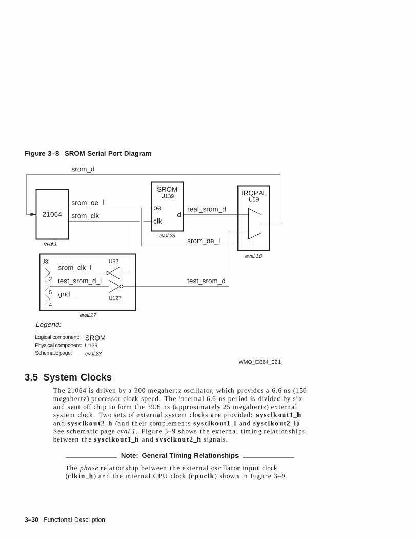
Figure 3–8 SROM Serial Port Diagram
WMO_EB64_021
srom_oe_l
J8
gnd
real_srom_d
Legend:
5
test_srom_d_l
eval.1
21064
srom_oe_l
2
srom_clk_l
srom_d
eval.27
srom_clk
4
U59
eval.18
IRQPAL
test_srom_d
U127
Physical component:Schematic page:
Logical component:
U52
U139
eval.23
SROM
U139
eval.23
SROM
oe
clkd
3.5 System ClocksThe 21064 is driven by a 300 megahertz oscillator, which provides a 6.6 ns (150megahertz) processor clock speed. The internal 6.6 ns period is divided by sixand sent off chip to form the 39.6 ns (approximately 25 megahertz) externalsystem clock. Two sets of external system clocks are provided: sysclkout1_hand sysclkout2_h (and their complements sysclkout1_l and sysclkout2_l)See schematic page eval.1. Figure 3–9 shows the external timing relationshipsbetween the sysclkout1_h and sysclkout2_h signals.
Note: General Timing Relationships
The phase relationship between the external oscillator input clock(clkin_h) and the internal CPU clock (cpuclk) shown in Figure 3–9
3–30 Functional Description

may not hold true. The figure should only be used to understand thegeneral timing relationships between the various clock signals.
Figure 3–9 System Clock Timing
WMO_EB64_012
6.6 ns
19.8 ns
39.6 ns
19.8 ns
13.2 ns
clkin 6¸
Delayed 1 cpuclk
cpuclk
Input
clkin_hOscillator
sysclkout2_h
sysclkout1_h
Internal
Figure 3–10 shows the clock distribution network for the EB64. The majorEB64 module clock is sysclkout1. It is initially sent to a phased locked loop(PLL) clock driver. The PLL creates four nearly identical copies of the signalwith low latency and skew from the original clock. The copies are distributedas follows:
• Two are sent to buffered clock drivers. Each clock driver generates ninecopies of the master system clock, which are sent throughout the EB64 todrive most of the control logic.
• One is sent to the memory control logic to drive one of the Bcache controlprogrammable logic devices (PLDs).
• One is sent to the expansion connector for customer use. See Section 4.2.3for more information about expansion connector clocks.
• A 2x (twice as fast) version of the system clock is sent to the SC486 tocontrol the ISA bus.
Functional Description 3–31

Figure 3–10 Clock Distribution
WMO_EB64_006
clock_in
SC486 ISA Controller
Memory Control Logic
Expansion Connector
MC88915
PLL
sysclk_pll_2x
sysclk_pll_4
sysclk_pll_3
Legend:
sysclkout1
Physical component:
Schematic page:
Logical component:
U146
eval.1
PLL
eval.1
21064eval.26
U146
sysclk_pll_2
sysclk_pll_1
eval.25
eval.25
buf_clk1_b<8:0>
buf_clk1_a<8:0>
clock_in
clock_in
10H645
10H645
BUFFER
BUFFER
U132
U134
buf_clk1_b2Expansion Connector
Note: Design Concepts
System design concepts are discussed in the application note Designinga System with the DECchip 21064 Microprocessor. Memory and backupcache design concepts are discussed in the application note Designinga Memory/Cache Subsystem for the DECchip 21064 Microprocessor. Ifyou are not familiar with the 21064, you are encouraged to read bothapplication notes. Appendix A gives ordering information and listsother associated documentation.
3–32 Functional Description

4Expansion Interface
This chapter describes the EB64 implementation of the 21064 externalinterface. It includes a description of the expansion connector signals anddesign considerations.
4.1 Expansion Connector Signal DescriptionTable 4–1 describes the signals available at the expansion connector. TheDECchip 21064 Microprocessor Hardware Reference Manual containsadditional information about expansion connector signals that are bufferedversions of the 21064 pinbus signals.
Table 4–1 Conventions
• Signal Name column — The ext_ prefix is ignored, and signals are listedalphabetically.
• I/O column — Signal direction, as follows:
I = input from expansion connector to EB64 logic (including 21064).O = output to expansion connector from EB64 logic (including 21064).B = bidirectional.
Expansion Interface 4–1

Table 4–1 Expansion Connector Signals
Signal Name Pin I/O Description
ext_adr33_in J26-B50 I External address bit 33. This signal is bufferedadr33 from the 21064. It is permanentlyenabled. Unlike the other signals on thisconnector, this is active high and has anassociated pull-down resistor. This signalis needed during DMA from the expansionconnector when the DMA engine wants toallocate a Bcache block for data, and theblock resides in the upper quadrant of thephysical address space. This bit allows theappropriate Bcache tag signal to be asserted. SeeSection 4.2.5.
ext_be1ext_be0
J27-B1J27-A1
O External unencoded transfer length. Thesesignals are used as adr<8:7> for logic attachedto the expansion connector that requires acontiguous linear address space. See ext_tl<1:0>and Section 3.1.3.1.
buf_clk1_b2 J26-B6 O Buffered system clock (see schematic pageseval.25 and eval.26). This clock is used when theexternal device uses four or less clock inputs (seeSection 4.2.3).
Clock sysclkout1 is a 25 MHz (39.6 ns) systemclock that synchronizes all clocked outputs.
buf_clk1_l J26-B7 O Buffered system clock. This signal is sysclk-out1_l buffered in the expansion connectorbuffers.
Clock sysclkout1 is a 25 MHz (39.6 ns) systemclock that synchronizes all clocked outputs.
buf_clk2 J26-B9 O Buffered delayed system clock. This signal issysclkout2 buffered in the expansion connectorbuffers.
buf_clk2_l J26-B10 O Buffered delayed system clock. This signal issysclkout2_l buffered in the expansion connectorbuffers.
buf_data<127:0> – B Buffered data. These signals are buffereddata<127:0> (see schematic page eval.3). SeeTable 4–3 for connector pin numbers.
(continued on next page)
4–2 Expansion Interface

Table 4–1 (Cont.) Expansion Connector Signals
Signal Name Pin I/O Description
buf_par3buf_par2buf_par1buf_par0
J11-A8J11-A10J11-B6J11-B8
B Buffered data parity. These signals are combinedand buffered to form check21, check14, check7,check0 to/from DRAM<3:0> and the 21064. SeeFigure 4–1
Note: The signal names change.
See Figure 4–1. At the input to U83 io.6, lw0_par<3:0> becomes gen_par<3:0>. The par<3:0>output of U133 mdlatch.5 becomes check21,check14, check7, and check0.
buf_tagctl_dbuf_tagctl_sbuf_tagctl_vbuf_tagctl_p
J26-A47J26-A45J26-A44J26-A48
O Buffered tag dirty, shared, and valid bits andtheir parity bit. These signals are tagctl_<d,s,v,p> buffered in the expansion connectorbuffers. These signals are always enabled. Theyallow logic on the expansion connector to performa Bcache probe (see also ext_hit and ext_tagctl_<d,s,v,p>_l>).
ext_cack2_lext_cack1_lext_cack0_l
J26-A39J26-A41J26-A42
I External cycle acknowledge. These signals areORed with io_cack<2:0> and memory statemachine signals in the memory state machineto generate cack<2:0> to the CPU. Cycleacknowledge is used to terminate all transactiontypes.
ext_cas3_lext_cas2_lext_cas1_lext_cas0_l
J11-B20J11-A25J11-B21J11-A26
I External column address strobe. These signalsare combined with io_cas<3:0> in the memorystate machine to generate early_cas<3:0>. Inturn, early_cas<3:0> is buffered and clockedwith sysclkout1 as buf1_dram_cas<8:0> toprovide the DRAMs with multiple versions of thesignals without excess skew.
When asserted, buf1_dram_cas<8:0> assertsCAS to the appropriate longword banks of thesystem DRAM array.�
�For more information, see the Designing a Memory/Cache Subsystem for the DECchip 21064 Microprocessorapplication note listed in Appendix A.
(continued on next page)
Expansion Interface 4–3

Table 4–1 (Cont.) Expansion Connector Signals
Signal Name Pin I/O Description
ext_clr_flag_l J11-A22 I External clear lock flag. This signal is ORedwith I/O signals in the I/O state machine togenerate io_clr_flag. One clock later, io_clr_flagis combined with memory state machine signalsin the RAS PAL to clear lock_flag. Signallock_flag clears two clocks after ext_clr_flag isasserted. See also Sections 3.2.3.4 and 3.2.3.5.
ext_col_a0_l J11-B23 I External column address 0. This signal controlsthe value of the least-significant address line tothe system DRAM. The interactions of this signalare described in Section 4.2.6.
ext_cwmask7ext_cwmask6ext_cwmask5ext_cwmask4ext_cwmask3ext_cwmask2ext_cwmask1ext_cwmask0
J26-B33J26-B34J26-B36J26-B37J26-B39J26-B40J26-B42J26-B43
O External cycle write mask. These signalsare cwmask<7:0> buffered in the expansionconnector buffers.
During CPU writes, write masks indicate whichof the eight 32-bit blocks are to be written.During CPU reads, the CPU provides informationon the miss that is being fulfilled. See theDECchip 21064 Microprocessor HardwareReference Manual for more information.
ext_data_a4_l J11-A15 I External data address 4. This signal is combinedwith other signals in the I/O state machine togenerate io_data_a4. Signal io_data_a4 is thencombined and registered in the memory statemachine to generate sys_data_a4.
This signal is asserted during accesses to theBcache. Signal sys_data_a4 is ORed with cpu_data_a4 from the 21064. As the least significantaddress line to the Bcache SRAMs, it selectsthe octaword of the cache block that is currentlyaddressed. It is used for victim writes andBcache block fills.
(continued on next page)
4–4 Expansion Interface

Table 4–1 (Cont.) Expansion Connector Signals
Signal Name Pin I/O Description
ext_data_oe_l J11-A39 I External data output enable. This signal iscombined with io_data_oe in the memory statemachine to generate sys_data_oe. Signal sys_data_oe is ORed with cpu_data_oe<3:0> fromthe 21064.
This signal is asserted to drive data and parityfrom the Bcache SRAMs onto the system dataand check lines. The data can be passed directlyto the CPU or can be clocked through the memorydata transceivers to the expansion connector orthe DRAM data bus.
ext_data_we3_lext_data_we2_lext_data_we1_lext_data_we0_l
J11-A40J11-B36J11-B37J11-B38
O External data write enable. These are longwordwrite strobes to the Bcache data SRAMs.�
These signals are combined with io_data_we<3:0> and registered in the memory statemachine to generate early_data_we<3:0>.Signals early_data_we<3:0> become sys_data_we<3:0> through delayed latches clocked bysysclkout1_l. Signals sys_data_we<3:0> areORed with cpu_data_we<3:0> from the 21064.
dcok J26-B12 O This signal is buffered p_dcok from powerconnector J3.
ext_del_creq2ext_del_creq1ext_del_creq0
J26-A30J26-A32J26-A33
O External delayed cycle request. These signals arebuffered del_creq<3:0> generated by creq<3:0>from the 21064 via clocked latches. Cycle requestis delayed by one CPU clock so that it can besampled using sysclkout1.
ext_dinvreq_l J11-A17 I External data cache invalidate request. Thissignal is ORed with io_dinvreq and memorystate machine signals in the memory statemachine to generate dinvreq to the 21064.
This signal is used to invalidate a data cacheentry when a Bcache block is evicted due to avictim write.
�For more information, see the Designing a Memory/Cache Subsystem for the DECchip 21064 Microprocessorapplication note listed in Appendix A.
(continued on next page)
Expansion Interface 4–5

Table 4–1 (Cont.) Expansion Connector Signals
Signal Name Pin I/O Description
ext_dmapwe J11-B15 O External data cache backmap write enable. Thissignal is dmapwe from the 21064 buffered in theexpansion connector buffers.
It controls the write enable to an optional,external, backmap RAM during external cachereads controlled by the 21064.
ext_doe_l J26-B30 I External data output enable. This signal iscombined with other signals in the memory statemachine to generate sm_doe_dis, which in turngenerates doe_dis.
This signal is asserted by external logic to allowthe 21064 to drive the data bus during externalwrite transactions. It is deasserted to allow avictim write sequence to proceed during a CPUwrite (the Bcache data SRAMs can then drivedata on the CPU data bus through the memorydata transceivers to the DRAM data bus). Seealso ext_data_oe_l.
Note: The signal names change.
See Figure 4–1. The doe_dis output of thememory state machine becomes the doe_l inputto the 21064.
ext_drack2_lext_drack1_lext_drack0_l
J26-A35J26-A36J26-A38
I External data bus read data acknowledge. Thesesignals are combined with io_drack<2:0> andmemory state machine signals in the memorystate machine to generate drack<2:0> to the21064.
These signals inform the 21064 whether data onthe data bus:
� Is valid.� Is cacheable.� Includes good parity.
(continued on next page)
4–6 Expansion Interface

Table 4–1 (Cont.) Expansion Connector Signals
Signal Name Pin I/O Description
ext_dwsel1_l J26-B31 I External data bus write select. This signal iscombined and registered in the memory statemachine to generate dwsel to the 21064.
During CPU write transactions, external logicuses this signal to tell the 21064 which part ofthe 32-byte write-data block to drive on the databus; it switches the CPU data bus from firstcache line data to second cache line data.
Note: The signal names change.
See Figure 4–1. Output dwsel of U117 mem.10becomes dwsel1.
gnd – – Ground. See Table 4–5 for pin list.
ext_hit J26-B45 O External cache hit. This signal is buffered hitfrom the memory state machine.
This signal is asserted on successful Bcachetag probe; that is, adr<33,25:19> from 21064matches tagadr<33,25:19>.
ext_hold_ack J26-B48 O External hold acknowledge. This signal isbuffered hold_ack from the 21064.
This signal is the handshake response to ext_hold_req. See Section 4.3 and Figure 4–5 forbus acquisition and release sequence.
ext_hold_l J26-B46 I External hold. This signal is used to get controlof the system bus from the memory statemachine.
Signal ext_hold and hold from the SC486 arecombined in the I/O state machine to generateio_hold which becomes hold in the memorystate machine. When the memory state machinenext reaches its idle state, it relinquishes buscontrol and asserts ext_start or dma_start.(Expansion bus always has priority over DMA,which represents the SC486). See Section 4.3and Figure 4–5 for bus acquisition and releasesequence.
Note: The signal names change.
See Figure 4–1. Signal io_hold changes to holdin the memory state machine.
(continued on next page)
Expansion Interface 4–7

Table 4–1 (Cont.) Expansion Connector Signals
Signal Name Pin I/O Description
ext_hold_req_l J26-A50 I External hold request. This signal is used inthe I/O state machine to generate hold_req tothe 21064. After ext_hold has been assertedto generate ext_start, hold_req is asserted toget control of the Bcache/external bus from the21064. See Section 4.3 and Figure 4–5 for busacquisition and release sequence.
ext_inhibit_tag_oe_l J11-A13 I External inhibit tag output enable.
In the memory state machine, this signal iscombined and registered to generate inhibit_tag_oe which is combined with io_inhibit_tag_oe to generate sys_tag_oe.
When deasserted, inhibit_tag_oe enables thetag and tag control values. This allows a hit/missto be determined, along with the current stateof the addressed Bcache block (S, V, D, P bits).Signal inhibit_tag_oe must be asserted duringa Bcache fill sequence, when new values arewritten into the tag and tag control SRAMs.
ext_ioadr_dis_l J26-B2 I External I/O address disable. This signal iscombined in the I/O state machine to generatemem_ioadr_dis which enables/disables the I/Oaddress bus through the CPU/IO address buffers.
When asserted, this signal disables the addressbuffers that drive I/O addresses (io_addr<31:2>)from the EB64 to the expansion connector. Thissignal is asserted during the bus acquisitionsequence by an external DMA device. It must beasserted before hold_ack can assert, because theassertion of hold_ack enables the buffers thatdrive in the opposite direction. See Section 4.3for the bus acquisition and release sequence.
(continued on next page)
4–8 Expansion Interface
Table 4–1 (Cont.) Expansion Connector Signals
Signal Name Pin I/O Description
io_addr<31:2> – B I/O address bus. These signals provide theaddress bus for DMA devices on the expansionconnector and for I/O accesses to devices on theexpansion connector. Note that the mappingbetween I/O address and CPU address signalsis different for a bus master (DMA device)and a bus slave (I/O device), as described inSection 3.1.3.1.
See Table 4–4 for connector pin numbers.
io_be3io_be2io_be1io_be0
J11-B9J11-B11J11-B12J11-B14
O I/O byte enables. These signals are combinationaldecodes of 21064 adr<8:5>, as described inSection 3.1.3.2. They can be used by externallogic to control byte masks for I/O write cycles.
ext_io_over_l J11-B18 I This signal is asserted by a DMA device on theexpansion connector to indicate that external useof the bus has completed.
It is combined in the I/O state machine togenerate io_over to the memory state machine.When io_over is detected, the memory statemachine resumes control of the system bus. SeeSection 4.3 and Figure 4–5 for bus acquisitionand release sequence.
ext_irq2_lext_irq1_lext_irq0_l
J11-A19J11-B17J11-A20
I External interrupt request lines. These signalsdrive cpu_irq<5:3> respectively to 21064through IRQ PAL delay.
Interrupt priority is a function of PALcode. Allinterrupts to the 21064 may be asynchronous andare level-sensitive.
ext_md_rd_clken_l J11-B26 I External memory data read clock enable. Thissignal is ORed with io_md_rd_clken andmemory state machine signals in the memorystate machine to generate md_rd_clken, whichenables the read data to be latched.�
�For more information, see the Designing a Memory/Cache Subsystem for the DECchip 21064 Microprocessorapplication note listed in Appendix A.
(continued on next page)
Expansion Interface 4–9

Table 4–1 (Cont.) Expansion Connector Signals
Signal Name Pin I/O Description
ext_md_rd_oe_l J11-A34 I External memory data read output enable.This signal is ORed with io_md_rd_oe andmemory state machine signals in the memorystate machine to generate md_rd_oe, whichenables the MDlatch to drive the Bcache/CPUdata bus.�
ext_md_wr_clken_l J11-A29 I External memory data write clock enable. Thissignal is ORed with io_md_wr_clken andmemory state machine signals in the memorystate machine to generate md_wr_clken, whichlatches data in the write direction.�
ext_md_wr_oe3_lext_md_wr_oe2_lext_md_wr_oe1_lext_md_wr_oe0_l
J11-A31J11-B27J11-A32J11-B29
I External memory data write output enable.These signals are ORed with io_md_wr_oe<3:0>and memory state machine signals in the memorystate machine to generate md_wr_oe<3:0>,which drives the buf_data<127:0> bus.�
ext_md_wr_par_oe_l J11-B30 I External memory data write parity outputenable. This signal is registered in the memorystate machine to generate md_wr_par_oe, whichdrives the buf_par<3:0> latch with parity.�
ext_ras_l J11-A23 I External row address strobe. This signal isORed with I/O, memory, and refresh signals inRAS PAL to generate dram_ras<1:0>. RASis asserted as a function of mux_adr<24,22>and the selected DRAM type, and is buffered tovarious chunks of the DRAM as buf<4:1>_dram_ras<1:0>.
remote_reset_l J26-B1 I When asserted, this signal resets the EB64 in thesame way as pressing a reset switch on the dcokheader (see Section 3.4.1). This allows circuitryattached to the expansion connector to reset thesystem (and itself) as a result of, for example,some form of fatal error or time out.
ext_reset_l J36-B13 O Buffered rst_l from reset/dcok circuit. (rst isthe EB64 master reset.) This signal is assertedas a result of any EB64 reset and should beused to reset circuitry attached to the expansionconnector.
�For more information, see the Designing a Memory/Cache Subsystem for the DECchip 21064 Microprocessorapplication note listed in Appendix A.
(continued on next page)
4–10 Expansion Interface

Table 4–1 (Cont.) Expansion Connector Signals
Signal Name Pin I/O Description
ext_sel_col_l J11-A28 I External select column. This signal is ORed withio_sel_col and memory state machine signals inthe memory state machine to generate sel_colwhich controls the DRAM address multiplexersfor all DRAM address lines.
When this signal is asserted, the system DRAMaddress multiplexers drive the column address,rather than the row address, into the DRAMarray.
ext_sel_col2_l J11-A16 I External select column 2. This signal is combinedwith I/O and memory state machine signalsin the memory state machine to generatedram_addr0. To avoid an additional externalmultiplexer delay, the memory state machinelogic implements all required dram_addr0multiplexing.
This signal is asserted during the transfer ofthe second cache line of a block into the systemDRAM. It is used to toggle the least significantCAS address bit during the page-mode secondCAS pulse of the DRAM cycle. The interactionsof this signal are described in Section 4.2.6.
ext_sel_tagadr_l J11-A14 I External select tag address. This signal iscombined and registered in the memory statemachine to generate sel_tagadr, used in theDRAM address multiplexers. When asserted,sel_tagadr causes data from the tag SRAMs(that is, the tag address) to be driven into thesystem DRAM row/column address multiplexer,rather than allowing the system address busto drive this multiplexer. This is necessary sothat a victim write sequence performed by logicattached to the expansion connector can generatethe correct address to retire a cache block fromthe Bcache to the system DRAM.
ext_start J26-A1 O This signal is the handshake response to ext_hold. Generated by the memory state machine,ext_start is a combinational signal and assertsin the same clock tick as io_hold. See Section 4.3and Figure 4–5 for bus acquisition and releasesequence.
(continued on next page)
Expansion Interface 4–11

Table 4–1 (Cont.) Expansion Connector Signals
Signal Name Pin I/O Description
sysclk_pll_3 J26-B4 O This signal is generated by sysclkout1 in thePLL (schematic page eval.26) for use with user-provided devices.
ext_tagadr_we_l J11-A11 I External tag address write enable. This signalis combined and registered in the memory statemachine to generate sys_tagadr_we. This signalis used to control the write strobe of the tagSRAMs during a Bcache block load. See alsoext_wrt_tagadr_oe_l.
ext_tagctl_d_lext_tagctl_s_lext_tagctl_v_lext_tagctl_p_l
J11-B33J11-A38J11-A37J11-B35
I External tag dirty, shared, and valid bits andtheir parity bit. These signals are combinedand registered with io_tagctl_<d,s,v,p> in thememory state machine to generate mem_tagctl_<d,s,v,p>.
These are Bcache tag control bits driven by logicattached to the expansion connector when thatlogic is writing data into the Bcache; for example,a read-fill or write-allocate sequence. Comparewith buf_tagctl_<d,s,v,p>.
ext_tagctl_we_l J11-B32 I External tag control write enable. This signalis combined and registered with io_tagctl_wein the memory state machine to generate sys_tagctl_we. Signal sys_tagctl_we is ORed withcpu_tagctl_we to control the write strobe of thetag control SRAMs during a Bcache block load.
Circuitry attached to the expansion connectorasserts this signal to update the tag control-bitvalues for the currently-addressed Bcache blockto the values driven on ext_tagctl_<d,s,v,p>_lwhen ext_wrt_tagctl_oe_l is asserted.
ext_tl1ext_tl0
J27-B50J27-A50
O External unencoded transfer length. Thesesignals are used as adr<6:5> for logic attachedto the expansion connector that requires acontiguous linear address space. See ext_be<1:0> and Section 3.1.3.1.
Vdd – – See Table 4–5 for pin list.
(continued on next page)
4–12 Expansion Interface
Table 4–1 (Cont.) Expansion Connector Signals
Signal Name Pin I/O Description
ext_we_l J11-B24 I External write enable. This signal is ORed withio_we and memory state machine signals in thememory state machine to generate dram_we.Signal dram_we is buffered as buf<4:1>_dram_we to write enable all banks of the DRAM.
wrap_read J27-B2 System register bit 21 (see Table 3–10). Thissignal is asserted to enable data wrapping on the21064. When wrapping is enabled, 21064 dataread accesses must use the cwmask1 signal todetermine which of the data portions to accessfirst (cwmask1 acts as adr4).
ext_wrt_tagadr_oe_l J11-B39 I External write tag address output enable. Thissignal is combined and registered in the memorystate machine to generate wrt_tagadr_oe. Itenables the system address onto the data busof the tag SRAMs. It is used to update the taginformation during a Bcache block fill. See alsoext_tagadr_we_l.
ext_wrt_tagctl_oe_l J11-A35 I External write tag control output enable. Thissignal is combined and registered with io_wrt_tagctl_oe in the memory state machineto generate wrt_tagctl_oe.
When asserted, this signal enables the values ofext_tagctl_<d,s,v,p> onto the data bus of thetag control SRAMs. It is used to update the tagcontrol information during a Bcache block fill.See also ext_tagctl_we_l.
ext_zone J26-B15 O External zone. This signal is asserted duringCPU accesses to the upper quadrant of physicalmemory (adr<33:32> = 11). For such cycles,the EB64 memory state machine waits, forever,if necessary, for signal io_over or the cycleacknowledge (cack<2:0>) signals to indicate theend of the cycle.
The I/O state machine generates ext_zone whenadr33 and adr32 are both asserted. Whenasserted, ext_zone indicates that this cycle is aslave cycle to a device in the expansion connectoraddress space.
Expansion Interface 4–13

Figure 4–1 Signal Name Changes
WMO_EB64_019
PARGEN
BUF
U130,U129
U23U91,U90
U157,U156
U159,U158
U34
lw3_par<3:0>
lw2_par<3:0>
lw1_par<3:0>
lw0_par<3:0>
DRAM<3:0>
io_par3
io_par2
io_par1
IO
io_par0
buf_par<3:0>
par_gen.1:4 par_gen.1 eval.3
eval.5,6
mdlatch.5
U133
eval.3
buf_par3
buf_par2
buf_par1
buf_par0
MDLATCH
par3
par2
par1
par0
check21
check14
check7
check0
gen_par3
U83
io.6
gen_par2
gen_par1
gen_par0
eval.18
MEM
U117
mem.10
ext_dwsel1_l
U126
mem.9
dwsel
doe_dis
dwsel1
doe_l
MEMDEC
MEM9
ext_dwsel1
io_hold
mem.1:6
holdU38,U56,U61,U68,U69,U82,
U135,U143,U144
U85
io.1
IO8
eval.19
hold
ext_hold_l ext_holdU128
eval.11
SC486
J26−B46
eval.9
Physical component:
Schematic page:
Functional block:
Logical component:
Legend:
U117
mem.10
MEM9
MEM
4–14 Expansion Interface

4.2 21064 Expansion InterfaceThe EB64 supplies a 21064-like protocol to a set of connectors on the board. Asshown in Figure 1–1, the signals are buffered versions of the system signals.Because these buffered signals are mostly isolated from the CPU signals, theyshould not affect operation in normal circumstances. The expansion connectorallows users to design their logic following a protocol similar to the 21064pinbus protocol and test it on real hardware.
The expansion interface includes signals that allow external logic to interactwith the CPU, the Bcache, and the DRAM. This allows options to be designedas either simple I/O devices (memory-mapped bus slaves that respond to buscycles from the 21064) or DMA devices (capable of acquiring control of the busfrom the 21064 and performing reads and writes directly to the Bcache andthe DRAM). The expansion interface control signals (Figure 4–2) are specialversions of existing memory control signals with an ext_ prefix.
Note: Expansion Control Signals Are Active Low
All control inputs from the expansion interface are asserted low andpulled up by on-board resistors. They are deasserted unless an externalmodule is plugged in and drives them. They also carry an _l suffix; forexample, ext_cack2_l.
Designing hardware to connect to the expansion connector requires most ofthe same knowledge as a 21064 design and is beyond the scope of this guide.Additional information is available in the EB64 schematics and programmable-logic source files, and also in the literature listed in Appendix A. Additionaltechnical support is available from the DECchip Information Line, alsodescribed in Appendix A.
The primary system considerations for external logic concern data path widthand cache coherency.
Expansion Interface 4–15

Figure 4–2 Expansion Interface Signals
WMO_EB64_007
Q
DQ
InternalFeedback
LocalInputs
ext_xxx_l
buf_sysclkout1 PLD
xxx
4.2.1 Data Path WidthThe EB64 uses the full, 128-bit width of the 21064 data path. Designinginterfaces to peripherals with narrower data path widths is not a problem, butthe system implications must be considered: It takes as many clock cycles totransfer 128-bits of data as it does to transfer any smaller number of bits. Inaddition, for DMA engines, an overhead is associated with bus acquisition andrelinquishment; every wasted clock cycle can equate to as many as 12 CPUinstructions (six clock cycles, two instructions/cycle).
4.2.2 Cache CoherencyExternal hardware must maintain cache coherency with the 21064 internalcaches (data cache and instruction cache) and the Bcache. The following aresome of a variety of hardware and software techniques that can be used tomaintain cache coherency.
4–16 Expansion Interface

1. I/O Devices
The simplest, and usually most desirable approach is to make I/O devicesnonBacheable by returning the appropriate values on ext_cack<2:0>_l.
2. Additional Memory
The expansion connector can be used to extend EB64 memory. Theadditional memory can be conventional DRAM or special-purpose memorysuch as dual-ported video RAM (VRAM). In these circumstances, a moreadvanced Bcache scheme may be desirable.
Because the EB64 DRAM main memory uses the Bcache, the way inwhich external slave devices can use the Bcache is limited. If circuitryon the expansion interface allocates Bcache blocks for addresses whereadr<33:32> = 11, it must never set the D (dirty) bit for these blocks(Section 3.2.2.1) because the EB64 memory controller would then need toreallocate the Bcache block. If the external circuitry had the capabilityto mark the block dirty, then the EB64 memory controller would have tobe able to perform victim write sequences to the memory on the externalboard, which it cannot do.
3. DMA Devices
For DMA devices there are more options. The simplest is to constrainthe DMA engine to perform transfers directly to the DRAM and to ignorethe Bcache. The 21064 must then access this data solely through thenonBcached aliases of the DRAM in the address space. This guaranteesthat cache coherency is maintained.
A more advanced design would need to perform a Bcache probe on DMAreads, and take data from the Bcache if there was a hit. Strictly, therequirement to maintain Bcache coherency is to take data if there was ahit and the Bcache is dirty. Otherwise, the data would be retrieved fromthe DRAM.
For DMA writes the design would have to:
• Probe the Bcache and, if there was a hit, merge the new data back intothe Bcache block. (The dirty bit should always be observed clear duringsuch a probe.)
• Clear the interlock flag.
• Invalidate the data cache.
Otherwise, the data would be stored to the DRAM. (A DMA engine doesnot usually write-allocate.)
Expansion Interface 4–17

4.2.3 Expansion Connector ClocksThe control signals coming from the expansion connector logic, that is, thecontrol signals generated by user hardware, are clocked by the master systemclock. This same clock drives the memory control logic on the EB64 board andis provided to the expansion connector to drive user hardware.
The EB64 system clock setup holds true for signals, such as ext_cack<2:0>_l,that eventually control other signals that are driven back to the 21064 withthe appropriate setup to the microprocessor system clock. The signals arerelatched by the board memory logic, making the setup time easy to achieve.
Figure 4–3 shows this relationship. The clocked device is a PLD, and theAND/OR plane feeds the flip-flop D input. Devices used on the EB64 boardrequire 10 ns setup before the clock. This allows several levels of logic to beplaced between the user expansion interface clock and the clock that is usedto resynchronize the external signals. This figure also shows the asserted lownature of the ext_xxx_l expansion connector control signals.
Figure 4–3 Expansion Connector Control Setup
WMO_EB64_023
Q
DQ
InternalFeedback
PLD
xxx
Q
buf_sysclkout1
DQ PLD
PLDext_xxx_l
Buffered versions of all four 21064 system clocks are delivered to the expansionconnector (buf_clk1_h/l, buf_clk2_h/l). When using these signals, carefulattention must be given to their skew with respect to other clock signals.Delayed and nondelayed versions of the master system clock (a version ofsysclkout1_h) are also sent to the expansion connector. These two signalsallow circuitry attached to the expansion connector to be clocked in a way that
4–18 Expansion Interface

is closely matched to the clocks on the EB64. To achieve this, signal loadingand board layout and characteristics requirements must be followed:
• The clock signals must have a characteristic impedance of 70 Ohms. Thiscan be achieved by using a controlled-impedance printed-circuit board andspecifying etch width and board layup (positioning of the internal powerand ground planes).
• Four or fewer nodes
The buf_clk1_b2 clock, if used, can be loaded by up to four nodes. If fewerthan four nodes load the net, dummy loads must be added in the form of 5pF capacitance for each missing load. The net must be routed so that thefour destination nodes are closely grouped and that the etch length fromthe expansion connector gold finger to each node is exactly 49 mm (2 in).
• More than four nodes
The sysclk_pll_3 clock, if used, must be routed through a clock bufferusing equivalent circuitry to that shown on schematic page eval.25. Theetch length from the expansion connector gold finger to the clock bufferinput pin must be exactly 49 mm (2 in). The series damping resistorson the clocks generated by the buffer must be situated so that the etchconnecting them to the buffer is short. Each net must then have the sameloading and layout characteristics as described for buf_clk1_b2 above. Theetch length from the series damping resistor to the destination node mustbe exactly 216.56 mm (8.526 in).
If these layout rules are adhered to, the total skew between any two buf_clk1_xx clocks in the system (EB64 and expansion connector) should not exceed 2.0ns (the specification of the H645 clock buffer devices). Furthermore, the totalclock fanout for the external board will be a maximum of 40 nodes.
4.2.4 Programmed I/O Through the Expansion ConnectorThis section gives an overview of the steps involved in performing reads andwrites to a device on the expansion connector. See Figure 4–4.
The external device for this example is a bank of video memory that isBcached on reads such that the S (shared) bit is always set by external logicon read fills. Therefore, Bcache blocks that get allocated to the video memoryalways behave as write-through. This means that they never become dirty.Consequently, a Bcache block currently allocated to the video memory canbe reallocated to the DRAM simply by overwriting the block (a victim writesequence is never needed). Conversely, when the external hardware allocates a
Expansion Interface 4–19
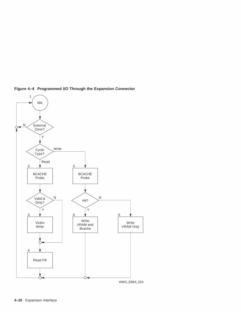
Figure 4–4 Programmed I/O Through the Expansion Connector
WMO_EB64_024
BCACHEProbe
Read
N
VictimWrite
Write WriteVRAM and VRAM OnlyBcache
Read Fill
Hit?Valid &Dirty?
ExternalZone?
Idle
Y
Write
N
BCACHEProbe
N
CycleType?
YY
1.
2.
3.
4.
5.
5. 5.
4–20 Expansion Interface

Bcache block to the video memory, it must potentially perform a victim write toretire that data to the system DRAM.
1. Idle Loop
Wait for a cycle addressed to video memory. The ext_zone signal willbe asserted for accesses to the upper quadrant of physical memory. Ifnecessary, some number of I/O address (io_addr) signals can also bedecoded. In addition to decoding ext_zone, decode del_creq<2:0> todetermine the cycle type. For read cycles, branch to step 2; for write cyclesbranch to step 5. For other cycles, some type of fatal error should probablybe generated.
If branching to step 5 (write cycle), prepare to latch data from the 21064 byasserting
ext_md_wr_oe_lext_md_wr_clken_lext_md_wr_par_oe_l
Prepare to write to the VRAM as appropriate. Assert ext_doe_l so thatthe 21064 will continue to drive write data.
The EB64 memory controller remains in a wait loop during the whole ofthe cycle. It automatically regains control of the system when it detectsext_cack<2:0>_l as no longer idle.
2. Read Cycle
Perform a Bcache probe. The Bcache tag control and tag address (tagctland tagadr) lines will be enabled, so this probe simply requires checkingthe appropriate tag control signals (buf_tagctl_v, buf_tagctl_d). Ifthe Bcache block is valid and dirty, a victim write sequence (step 3) isnecessary. Otherwise, proceed with the read fill (step 4).
If branching to step 3, assert ext_sel_tagadr_l so that the address intothe system DRAM is generated in part by the tag address lines; that is,the system DRAM is being addressed at the correct location for the victimwrite of the Bcache block.
3. Victim Write Sequence
Retire the valid, dirty Bcache block to the system DRAM so that thisBcache block can be filled with data from VRAM. The following signalsneed to be manipulated:
• ext_ras_lext_cas<3:0>_lext_we_l
to actually write to the system DRAM.
Expansion Interface 4–21

• ext_data_oe_l so that the Bcache data SRAMs will drive their datainto the DRAMs.
• ext_md_wr_oe<3:0>_lext_md_wr_par_oe_lmd_wr_clken_l
to transfer the data from the CPU data bus (where it is being drivenby the Bcache data SRAMs) through the memory data transceivers(MDlatch) to the DRAM data bus.
• ext_data_a4_l to select the second location in Bcache to access thesecond 128-bit octaword of data.
• ext_sel_col_l to select the DRAM column address.
• ext_sel_col2_l to select the second column address for the adjacentlocation in DRAM, which is the destination of the second 128-bitoctaword of data (this data is written as a page-mode access to theDRAM).
When the victim write sequence is complete, continue with step 4, the readfill sequence.
4. Read Fill Sequence
Either fall through to this step after a victim write sequence (step 3) orjump to this step as the result of a read where the associated Bcache blockis not valid or not dirty (step 2).
This sequence requires the manipulation of the appropriate user signalsto retrieve data from the VRAM on the external board. It requiresmanipulating the following signals:
• ext_inhibit_tag_oe_lext_md_rd_oe_lext_md_rd_clken_l
so that the VRAMs on the external board can drive new data throughthe memory data transceivers (MDlatch) and into the Bcache dataSRAMs.
• ext_wrt_tagctl_oe_lext_wrt_tagadr_oe_lext_tagctl_v_lext_tagctl_s_l
to assert the appropriate tag control bits and drive them into theBcache tag control SRAMs.
4–22 Expansion Interface

• ext_data_we<3:0>_lext_tagctl_we_lext_tagadr_we_l
to write new data into the Bcache data, tag address, and tag controlSRAMs. The tag address itself is still being driven by the 21064 onits address bus. Signal ext_drack<2:0>_l needs to be manipulated tosimultaneously pass the data to the 21064.
• ext_data_a4_l to select the second location in the Bcache data SRAM.
• ext_dinvreq_l may have to be manipulated to invalidate a 21064internal data cache block.
• ext_cack<2:0>_l to terminate the 21064 read cycle.
5. Write Block
Perform a Bcache probe. As for the read cycle, this simply requireschecking the appropriate signals. If a Bcache hit is detected (ext_hitasserted) the data is written to VRAM (on the external connector logic) andto the appropriate Bcache block. The Bcache behaves as write-through forVRAM data because video memory is always required to be up-to-date. Ifa Bcache miss is detected, data is written only to VRAM. A write-allocateis never done, and there is no victim sequence for writes. In practice, thesame sequence can be used for the Bcache miss and the Bcache hit byconditionally asserting ext_data_we<3:0>_l (the write strobes to Bcache).The write sequence involves manipulating the following signals:
• ext_doe_lext_md_wr_oe<3:0>_lext_md_wr_clken_lext_md_wr_par_oe_lext_dwsel1_l
to transfer the two 128-bit octawords of data from the 21064 to theBcache and expansion connector data busses.
• Appropriate user signals on the external connector logic in order towrite the data to the VRAM.
• ext_data_a4_l to address the second location in the Bcache.
• ext_cack<2:0>_l to terminate the 21064 write cycle.
The EB64 memory controller remains in a wait loop during the whole ofthe cycle. It automatically regains control of the system when it detectsext_cack<2:0>_l as no longer idle.
Expansion Interface 4–23

4.2.5 DMA Through Expansion ConnectorThis section provides an overview of steps involved in performing read andwrite DMA transfers from a device on the expansion connector.
The external device is assumed to be transferring data to and from the EB64main memory in response to an input stimuli. The transfers go directly tothe DRAM main memory. The procedure for a system that requires Bcacheprobes can be derived from the programmed I/O example in Section 4.2.4. Inaddition to the Bcache control signals, the memory data transceiver (MDlatch)controls must be manipulated in order to transfer data between the Bcachedata bus and the DRAM data bus, which is directly connected to the expansionconnector data bus.
The bus acquisition and release sequences are described in Section 4.3.
1. Bus Acquisition
a. Assert ext_hold_l and wait for the memory controller to complete itscurrent bus cycle, indicated by a pulse of one clock period duration onext_start.
b. After ext_start has pulsed, gain control of the 21064 bus by assertingext_hold_req and waiting for ext_hold_ack.
c. While waiting for ext_hold_ack to assert, ext_ioadr_dis must beasserted in order to tristate the I/O address bus (io_addr) on theexpansion connector.
Note: Avoiding Bus Contention
This timing is important. The asserted level of ext_hold_ack willdrive io_addr in the opposite direction; therefore, ext_ioadr_dis musthave been asserted earlier in order to avoid bus contention.
2. Data Transfers
a. Data Read Transfer
During this sequence a number of data units are read from the DRAMmain memory and transferred to some data sink on the externalconnector logic. When a number of 128-bit data chunks are to betransferred, the transfer can be performed in DRAM page-mode.(This imposes some constraints in that a page boundary must not becrossed.) The sequence requires manipulating the ext_ras_l, ext_cas<3:0>_l, and ext_sel_col_l signals, with the I/O address bus (io_addr) supplying the row and then all subsequent column addresses.
4–24 Expansion Interface

The least significant column address line is controlled by either ext_col_a0 or ext_sel_col2_l. The DRAM data lines are wired directly tothe expansion connector.
Note: DRAM Refresh Requirements
The DMA engine cannot retain control of the bus for extended periods;doing so would compromise the CAS-before-RAS DRAM refresh cyclesthat must be performed under control of the memory controller.
b. Data Write Transfer
During this sequence a number of data units are read from some datasource on the external connector logic and written into the DRAM mainmemory. The procedure is the same as for data read transfers (step2.a), with the addition that ext_data_we<3:0>_l must be appropriatelymanipulated. Note that, on DMA writes to the DRAM main memory, aparity bit must be generated for each longword (four bytes) written.
Because some external device has had control of the bus, it may benecessary to clear the system lock flag. The lock flag is cleared bypulsing ext_clr_flag_l for one clock period.
3. Bus Release
Deassert io_addr_dis. Deassert ext_hold_req and assert ext_io_over forone clock cycle. This action signals the memory controller that it shouldregain control of the bus.
4.2.6 DRAM Address 0Sections 3.2.1.1 through 3.2.1.4 give a functional description of DRAMaddressing. This section gives an overview of the steps involved in generatingDRAM address 0 from the 21064 and from a DMA device attached to theexpansion connector.
Most of the DRAM address lines are switched between row and columnaddresses using a bank of multiplexers (schematic page addr_mux.1). ForDRAM address 0, the column address must be switched from one value toanother in order to page-mode access each 128-bits of the hexaword. Thisswitching, along with the row and column multiplexing, is performed in thememory controller according to the following equation:
Expansion Interface 4–25

DRAM_ADDR0 = (!IO_WAIT & ADR13 & !SEL_COL & !SEL_COL2) #(!IO_WAIT & FIRST_COL_A0 & SEL_COL & !SEL_COL2) #(!IO_WAIT & !FIRST_COL_A0 & SEL_COL2) #( IO_WAIT & ADR13 & !SEL_COL) #( IO_WAIT & IO_COL_A0 & SEL_COL) #( IO_WAIT & EXT_COL_A0 & SEL_COL & !EXT_SEL_COL2) #( IO_WAIT & !EXT_COL_A0 & SEL_COL & EXT_SEL_COL2);
The individual lines (product terms) of this equation behave as follows:
• 21064 Access to DRAM (not io_wait)
1. Select the row address, adr13.
2. Do one of the following:
– If a wrapped cycle is being performed (first_col_a0 asserted),select the column address. The first column address strobed intothe DRAM will be 1 (odd address); the second, when sel_col2 isasserted, will be 0 (even address).
– If a nonwrapped cycle is being performed (first_col_a0 deasserted),select the column address. The first column address strobed intothe DRAM will be 0 (even address); the second, when sel_col2 isasserted, will be 1 (odd address). Assertion of sel_col2 impliesassertion of sel_col; therefore, sel_col is not required.
• DMA Device Access to the DRAM (io_wait)
The following steps are used during DMA accesses to the DRAM or duringaccesses to the upper quadrant of physical memory; that is, the expansionconnector address space.
1. Select the row address, adr13.
2. Do one of the following:
– Select the column address. Controlled by the EB64 I/O controllerduring DMA transfers by the SC486.
– Select the column address. Controlled by signals from theexpansion connector interface. When sel_col is asserted (as aresult of ext_sel_col), ext_col_a0 directly controls the value of theleast significant DRAM column address. Signal ext_sel_col2 isassumed to be deasserted.
– Select the column address. Controlled by signals from theexpansion connector interface. When sel_col is asserted (as aresult of ext_sel_col), ext_col_a0 is set to select the first DRAMcolumn address (either 0 or 1); then ext_sel_col2 toggles to select
4–26 Expansion Interface
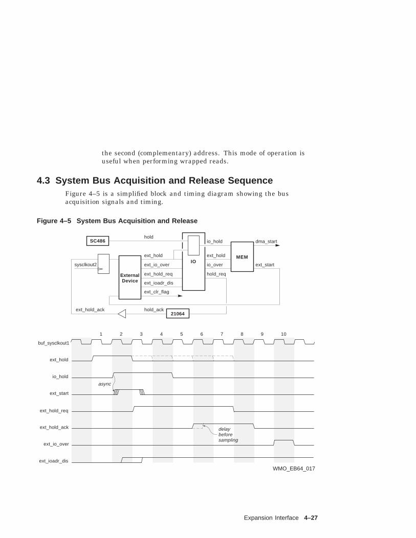
the second (complementary) address. This mode of operation isuseful when performing wrapped reads.
4.3 System Bus Acquisition and Release SequenceFigure 4–5 is a simplified block and timing diagram showing the busacquisition signals and timing.
Figure 4–5 System Bus Acquisition and Release
WMO_EB64_017
buf_sysclkout1
1 2 3 4 5 6 7 8 9 10
delaybeforesampling
ext_ioadr_dis
ext_io_over
ext_hold_ack
ext_hold_req
ext_start
ext_hold
io_hold
ext_hold
ext_ioadr_dis
ext_hold_req
21064
ext_clr_flag
hold
ext_io_over
ext_hold
hold_req
io_over
io_hold dma_start
ext_startsysclkout2
ext_hold_ack hold_ack
SC486
IOMEM
ExternalDevice
async
Expansion Interface 4–27

The acquisition sequence is:
1. Assert ext_hold.
2. Wait for ext_start.
3. Assert ext_hold_req.
4. Wait for ext_hold_ack.
5. Perform bus operations.
Note that ext_start is asserted for only one clock tick, and that ext_holdshould be deasserted as soon as ext_start is detected.
The release sequence is:
1. Deassert ext_hold_req (ext_hold_ack deasserts).
2. Assert ext_io_over for one clock tick.
4.4 Expansion Connector Pin Lists
Table 4–2 Expansion Connector Pin List
Pin Signal Pin Signal
J10-A1 not connected J10-B1 buf_dat62J10-A2 buf_dat63 J10-B2 buf_dat60J10-A3 Vdd J10-B3 buf_dat58J10-A4 buf_dat61 J10-B4 gndJ10-A5 buf_dat59 J10-B5 buf_dat56J10-A6 gnd J10-B6 buf_dat54J10-A7 buf_dat57 J10-B7 VddJ10-A8 buf_dat55 J10-B8 buf_dat52J10-A9 Vdd J10-B9 buf_dat50J10-A10 buf_dat53 J10-B10 gndJ10-A11 buf_dat51 J10-B11 buf_dat48J10-A12 gnd J10-B12 buf_dat46J10-A13 buf_dat49 J10-B13 VddJ10-A14 buf_dat47 J10-B14 buf_dat44J10-A15 buf_dat45 J10-B15 buf_dat42J10-A16 buf_dat43 J10-B16 gndJ10-A17 buf_dat41 J10-B17 buf_dat40J10-A18 gnd J10-B18 buf_dat38
(continued on next page)
4–28 Expansion Interface

Table 4–2 (Cont.) Expansion Connector Pin List
Pin Signal Pin Signal
J10-A19 buf_dat39 J10-B19 not connectedJ10-A20 buf_dat37 J10-B20 buf_dat36J10-A21 Vdd J10-B21 buf_dat34J10-A22 buf_dat35 J10-B22 gndJ10-A23 buf_dat33 J10-B23 buf_dat32J10-A24 gnd J10-B24 buf_dat30J10-A25 buf_dat31 J10-B25 VddJ10-A26 buf_dat29 J10-B26 buf_dat28J10-A27 Vdd J10-B27 buf_dat26J10-A28 buf_dat27 J10-B28 gndJ10-A29 buf_dat25 J10-B29 buf_dat24J10-A30 gnd J10-B30 buf_dat22J10-A31 buf_dat23 J10-B31 VddJ10-A32 buf_dat21 J10-B32 buf_dat20J10-A33 Vdd J10-B33 buf_dat18J10-A34 buf_dat19 J10-B34 gndJ10-A35 buf_dat17 J10-B35 buf_dat16J10-A36 gnd J10-B36 buf_dat14J10-A37 buf_dat15 J10-B37 buf_dat12J10-A38 buf_dat13 J10-B38 buf_dat10J10-A39 buf_dat11 J10-B39 buf_dat 8J10-A40 buf_dat 9 J10-B40 not connected
J11-A1 not connected J11-B1 buf_dat 6J11-A2 buf_dat 7 J11-B2 buf_dat 4J11-A3 Vdd J11-B3 buf_dat 2J11-A4 buf_dat 5 J11-B4 gndJ11-A5 buf_dat 3 J11-B5 buf_dat 0J11-A6 gnd J11-B6 buf_par1J11-A7 buf_dat 1 J11-B7 VddJ11-A8 buf_par3 J11-B8 buf_par0J11-A9 Vdd J11-B9 io_be3J11-A10 buf_par2 J11-B10 gndJ11-A11 ext_tagadr_we_l J11-B11 io_be2J11-A12 gnd J11-B12 io_be1J11-A13 ext_inhibit_tag_oe_l J11-B13 VddJ11-A14 ext_sel_tagadr_l J11-B14 io_be0J11-A15 ext_data_a4_l J11-B15 ext_dmapweJ11-A16 ext_sel_col2_l J11-B16 gnd
(continued on next page)
Expansion Interface 4–29

Table 4–2 (Cont.) Expansion Connector Pin List
Pin Signal Pin Signal
J11-A17 ext_dinvreq_l J11-B17 ext_irq1_lJ11-A18 gnd J11-B18 ext_io_over_lJ11-A19 ext_irq2_l J11-B19 not connectedJ11-A20 ext_irq0_l J11-B20 ext_cas3_lJ11-A21 Vdd J11-B21 ext_cas1_lJ11-A22 ext_clr_flag_l J11-B22 gndJ11-A23 ext_ras_l J11-B23 ext_col_a0_lJ11-A24 gnd J11-B24 ext_we_lJ11-A25 ext_cas2_l J11-B25 VddJ11-A26 ext_cas0_l J11-B26 ext_md_rd_clken_lJ11-A27 Vdd J11-B27 ext_md_wr_oe2_lJ11-A28 ext_sel_col_l J11-B28 gndJ11-A29 ext_md_wr_clken_l J11-B29 ext_md_wr_oe0_lJ11-A30 gnd J11-B30 ext_md_wr_par_oe_lJ11-A31 ext_md_wr_oe3_l J11-B31 VddJ11-A32 ext_md_wr_oe1_l J11-B32 ext_tagctl_we_lJ11-A33 Vdd J11-B33 ext_tagctl_d_lJ11-A34 ext_md_rd_oe_l J11-B34 gndJ11-A35 ext_wrt_tagctl_oe_l J11-B35 ext_tagctl_p_lJ11-A36 gnd J11-B36 ext_data_we2_lJ11-A37 ext_tagctl_v_l J11-B37 ext_data_we1_lJ11-A38 ext_tagctl_s_l J11-B38 ext_data_we0_lJ11-A39 ext_data_oe_l J11-B39 ext_wrt_tagadr_oe_lJ11-A40 ext_data_we3_l J11-B40 not connected
J26-A1 ext_start J26-B1 remote_reset_lJ26-A2 io_addr25 J26-B2 ext_ioadr_dis_lJ26-A3 io_addr24 J26-B3 io_addr2J26-A4 Vdd J26-B4 sysclk_pll_3J26-A5 io_addr23 J26-B5 gndJ26-A6 io_addr22 J26-B6 buf_clk1_b2J26-A7 gnd J26-B7 buf_clk1_lJ26-A8 io_addr21 J26-B8 VddJ26-A9 io_addr20 J26-B9 buf_clk2J26-A10 Vdd J26-B10 buf_clk2_lJ26-A11 io_addr19 J26-B11 gndJ26-A12 io_addr18 J26-B12 dcokJ26-A13 gnd J36-B13 ext_reset_lJ26-A14 io_addr17 J26-B14 Vdd
(continued on next page)
4–30 Expansion Interface

Table 4–2 (Cont.) Expansion Connector Pin List
Pin Signal Pin Signal
J26-A15 io_addr16 J26-B15 ext_zoneJ26-A16 Vdd J26-B16 io_addr3J26-A17 io_addr15 J26-B17 gndJ26-A18 io_addr14 J26-B18 io_addr31J26-A19 gnd J26-B19 io_addr30J26-A20 io_addr13 J26-B20 VddJ26-A21 io_addr12 J26-B21 io_addr29J26-A22 Vdd J26-B22 io_addr28J26-A23 io_addr11 J26-B23 gndJ26-A24 io_addr10 J26-B24 io_addr27J26-A25 gnd J26-B25 io_addr26J26-A26 io_addr 9 J26-B26 VddJ26-A27 io_addr 8 J26-B27 io_addr7J26-A28 Vdd J26-B28 io_addr6J26-A29 io_addr5 J26-B29 gndJ26-A30 ext_del_creq2 J26-B30 ext_doe_lJ26-A31 gnd J26-B31 ext_dwsel1_lJ26-A32 ext_del_creq1 J26-B32 VddJ26-A33 ext_del_creq0 J26-B33 ext_cwmask7J26-A34 Vdd J26-B34 ext_cwmask6J26-A35 ext_drack2_l J26-B35 gndJ26-A36 ext_drack1_l J26-B36 ext_cwmask5J26-A37 gnd J26-B37 ext_cwmask4J26-A38 ext_drack0_l J26-B38 VddJ26-A39 ext_cack2_l J26-B39 ext_cwmask3J26-A40 Vdd J26-B40 ext_cwmask2J26-A41 ext_cack1_l J26-B41 gndJ26-A42 ext_cack0_l J26-B42 ext_cwmask1J26-A43 gnd J26-B43 ext_cwmask0J26-A44 buf_tagctl_v J26-B44 VddJ26-A45 buf_tagctl_s J26-B45 ext_hitJ26-A46 Vdd J26-B47 gndJ26-A47 buf_tagctl_d J26-B46 ext_hold_lJ26-A48 buf_tagctl_p J26-B48 ext_hold_ackJ26-A49 gnd J26-B49 io_addr4J26-A50 ext_hold_req_l J26-B50 ext_adr33_in
J27-A1 ext_be0 J27-B1 ext_be1J27-A2 buf_dat127 J27-B2 wrap_read
(continued on next page)
Expansion Interface 4–31
Table 4–2 (Cont.) Expansion Connector Pin List
Pin Signal Pin Signal
J27-A3 buf_dat125 J27-B3 buf_dat126J27-A4 Vdd J27-B4 buf_dat124J27-A5 buf_dat123 J27-B5 gndJ27-A6 buf_dat121 J27-B6 buf_dat122J27-A7 gnd J27-B7 buf_dat120J27-A8 buf_dat119 J27-B8 VddJ27-A9 buf_dat117 J27-B9 buf_dat118J27-A10 Vdd J27-B10 buf_dat116J27-A11 buf_dat115 J27-B11 gndJ27-A12 buf_dat113 J27-B12 buf_dat114J27-A13 gnd J27-B13 buf_dat112J27-A14 buf_dat111 J27-B14 VddJ27-A15 buf_dat109 J27-B15 buf_dat110J27-A16 Vdd J27-B16 buf_dat108J27-A17 buf_dat107 J27-B17 gndJ27-A18 buf_dat105 J27-B18 buf_dat106J27-A19 gnd J27-B19 buf_dat104J27-A20 buf_dat103 J27-B20 VddJ27-A21 buf_dat101 J27-B21 buf_dat102J27-A22 Vdd J27-B22 buf_dat100J27-A23 buf_dat 99 J27-B23 gndJ27-A24 buf_dat 97 J27-B24 buf_dat 98J27-A25 gnd J27-B25 buf_dat 96J27-A26 buf_dat95 J27-B26 VddJ27-A27 buf_dat93 J27-B27 buf_dat94J27-A28 Vdd J27-B28 buf_dat92J27-A29 buf_dat91 J27-B29 gndJ27-A30 buf_dat89 J27-B30 buf_dat90J27-A31 gnd J27-B31 buf_dat88J27-A32 buf_dat87 J27-B32 VddJ27-A33 buf_dat85 J27-B33 buf_dat86J27-A34 Vdd J27-B34 buf_dat84J27-A35 buf_dat83 J27-B35 gndJ27-A36 buf_dat81 J27-B36 buf_dat82J27-A37 gnd J27-B37 buf_dat80J27-A38 buf_dat79 J27-B38 VddJ27-A39 buf_dat77 J27-B39 buf_dat78J27-A40 Vdd J27-B40 buf_dat76J27-A41 buf_dat75 J27-B41 gnd
(continued on next page)
4–32 Expansion Interface

Table 4–2 (Cont.) Expansion Connector Pin List
Pin Signal Pin Signal
J27-A42 buf_dat73 J27-B42 buf_dat74J27-A43 gnd J27-B43 buf_dat72J27-A44 buf_dat71 J27-B44 VddJ27-A45 buf_dat69 J27-B45 buf_dat70J27-A46 Vdd J27-B46 buf_dat68J27-A47 buf_dat67 J27-B47 gndJ27-A48 buf_dat65 J27-B48 buf_dat66J27-A49 gnd J27-B49 buf_dat64J27-A50 ext_tl0 J27-B50 ext_tl1
Table 4–3 Expansion Connector Pin List — buf_data<127:0>
Bit Pin Bit Pin Bit Pin Bit Pin
127 J27-A2 95 J27-A26 63 J10-A2 31 J10-A25126 J27-B3 94 J27-B27 62 J10-B1 30 J10-B24125 J27-A3 93 J27-A27 61 J10-A4 29 J10-A26124 J27-B4 92 J27-B28 60 J10-B2 28 J10-B26123 J27-A5 91 J27-A29 59 J10-A5 27 J10-A28122 J27-B6 90 J27-B30 58 J10-B3 26 J10-B27121 J27-A6 89 J27-A30 57 J10-A7 25 J10-A29120 J27-B7 88 J27-B31 56 J10-B5 24 J10-B29119 J27-A8 87 J27-A32 55 J10-A8 23 J10-A31118 J27-B9 86 J27-B33 54 J10-B6 22 J10-B30117 J27-A9 85 J27-A33 53 J10-A10 21 J10-A32116 J27-B10 84 J27-B34 52 J10-B8 20 J10-B32115 J27-A11 83 J27-A35 51 J10-A11 19 J10-A34114 J27-B12 82 J27-B36 50 J10-B9 18 J10-B33113 J27-A12 81 J27-A36 49 J10-A13 17 J10-A35112 J27-B13 80 J27-B37 48 J10-B11 16 J10-B35111 J27-A14 79 J27-A38 47 J10-A14 15 J10-A37110 J27-B15 78 J27-B39 46 J10-B12 14 J10-B36109 J27-A15 77 J27-A39 45 J10-A15 13 J10-A38108 J27-B16 76 J27-B40 44 J10-B14 12 J10-B37107 J27-A17 75 J27-A41 43 J10-A16 11 J10-A39106 J27-B18 74 J27-B42 42 J10-B15 10 J10-B38105 J27-A18 73 J27-A42 41 J10-A17 9 J10-A40104 J27-B19 72 J27-B43 40 J10-B17 8 J10-B39103 J27-A20 71 J27-A44 39 J10-A19 7 J11-A2
(continued on next page)
Expansion Interface 4–33

Table 4–3 (Cont.) Expansion Connector Pin List — buf_data<127:0>
Bit Pin Bit Pin Bit Pin Bit Pin
102 J27-B21 70 J27-B45 38 J10-B18 6 J11-B1101 J27-A21 69 J27-A45 37 J10-A20 5 J11-A4100 J27-B22 68 J27-B46 36 J10-B20 4 J11-B299 J27-A23 67 J27-A47 35 J10-A22 3 J11-A598 J27-B24 66 J27-B48 34 J10-B21 2 J11-B397 J27-A24 65 J27-A48 33 J10-A23 1 J11-A796 J27-B25 64 J27-B49 32 J10-B23 0 J11-B5
Table 4–4 Expansion Connector Pin List — io_addr<31:2>
Bit Pin Bit Pin Bit Pin Bit Pin
31 J26-B18 23 J26-A5 15 J26-A17 7 J26-B2730 J26-B19 22 J26-A6 14 J26-A18 6 J26-B2829 J26-B21 21 J26-A8 13 J26-A20 5 J26-A2928 J26-B22 20 J26-A9 12 J26-A21 4 J26-B4927 J26-B24 19 J26-A11 11 J26-A23 3 J26-B1626 J26-B25 18 J26-A12 10 J26-A24 2 J26-B325 J26-A2 17 J26-A14 9 J26-A2624 J26-A3 16 J26-A15 8 J26-A27
Table 4–5 Expansion Connector Pin List — Vdd and gnd
Connector gnd Pins Vdd Pins
J26/J27 A7 B5 A4 B8J26/J27 A13 B11 A10 B14J26/J27 A19 B17 A16 B20J26/J27 A25 B23 A22 B26J26/J27 A31 B29 A28 B32J26/J27 A37 B35 A34 B38J26/J27 A43 B41 A40 B44J26/J27 A49 B47 A46
J10/J11 A6 B4 A3 B7J10/J11 A12 B10 A9 B13J10/J11 A18 B16 A21 B25J10/J11 A24 B22 A27 B31
(continued on next page)
4–34 Expansion Interface

Table 4–5 (Cont.) Expansion Connector Pin List — Vdd and gnd
Connector gnd Pins Vdd Pins
J10/J11 A30 B28 A33J10/J11 A36 B34
Expansion Interface 4–35


5Power Requirements
The EB64 derives its main system power from a user-supplied, industry-standard, PC power supply. It consumes 18 A of power. To calculate powersupply needs for your system, add the current requirements (in amps) for eachvoltage required by each device installed in the system to the value of the rawEB64 board (18 A). Table 5–1 shows amps for each voltage.
Table 5–1 Voltage/Amp
Volts Amps
5 V 18 A
-5 V 0 A
-12 V .3 A
+12 V 1 A
See Section 3.4 and schematic pages eval.16, eval.24, and eval.29 for moreinformation.
Caution: Fan Sensor Required
The 21064 cooling fan must have a built-in sensor that will drive asignal if the air flow stops. The sensor is connected to the EB64 board(J17 Figure 2–1 and Table 2–1). When the signal is generated, itplaces the system into dcok mode. This action protects the CPU underfan-failure conditions, because the 21064 dissipates less heat in dcokmode. The fan supplied with the EB64 includes an air-flow sensor.
Power Requirements 5–1

ATechnical Support, Ordering, and
Associated Literature
This appendix explains how to:
• Call for DECchip information and technical support.
• Order DECchip parts.
• Order associated literature for the DECchip 21064 evaluation board andthe DECchip 21064 microprocessor.
Technical Support, Ordering, and Associated Literature A–1

A.1 Information and Technical SupportCall the following phone numbers for information and technical support:
United States and CanadaTTY (United States only)Outside North America
1–800–332–2717 (1–800–DEC–2717)1–800–332–2515 (1–800–DEC–2515)+1–508–568–6868
A.2 Ordering DECchip ProductsTo order the DECchip 21064 and related products, contact your local Digitalsales office. Working with your sales representative, you may be able to takeadvantage of discounts and volume pricing.
You can order the following DECchip products from Digital.
Product Speed Order Number
DECchip 21064 Microprocessor 150 MHz 21064–AA
DECchip 21064 Microprocessor 200 MHz 21064–BA
DECchip 21064 Sample Kit 150 MHz 21064–SA
DECchip 21064 Sample Kit 200 MHz 21064–SB
Heat Sink Assembly – 2106H–AA
A.3 Associated DECchip LiteratureThe following table lists DECchip literature in the these categories:
• DECchip 21064 Literature
• DECchip 21064 Evaluation Board Literature
• DECchip Marketing Literature
A–2 Technical Support, Ordering, and Associated Literature
Title Order Number
DECchip 21064 Literature
DECchip 21064 Microprocessor Data Sheet EB–N0136–72
DECchip 21064 Microprocessor Hardware ReferenceManual
EC–N0079–72
DECchip 21064 PALcode System Design Guide EC–N0543–72
Designing a Memory/Cache Subsystem for theDECchip 21064 Microprocessor: An Application Note
EC–N0301–72
Designing a System with the DECchip 21064Microprocessor: An Application Note
EC–N0107–72
DECchip 21064 Evaluation Board Literature
Calculating a System I/O Address for the DECchip 21064Evaluation Board: An Application Note
EC–N0567–72
DECchip 21064 Bus Transactor User’s Guide EC–N0448–72
DECchip 21064 Evaluation Board Debug MonitorUser’s Guide
EC–N0392–72
DECchip 21064 Evaluation Board Design PackageRead Me First
EC–N0352–72
DECchip 21064 Evaluation Board Product Brief EC–N0353–72
DECchip 21064 SROM Mini-Debugger User’s Guide EC–N0357–72
DECchip 21064 Evaluation Board User’s Guide EC–N0351–72
DECchip 21064 Software Design Tools User’s Guide EC–N0441–72
DECchip Marketing Literature
AMP PGA Burn-In and Product Sockets for DECchip21064 with Alpha AXP Architecture AXP
EC–X3013–72
DECchip Information Line Brochure EB–N0109–72
DECchip Preprocessor for Hewlett-Packard LogicAnalyzer
EC–X2454–72
DECchip Sample Kit Brochure EB–N0108–72
Technical Support, Ordering, and Associated Literature A–3

Ordering Associated DECchip LiteratureTo order any of the previously listed DECchip literature, use FAX or mail.
FAX (available 24 hours)
1–508–351–4467
Digital Equipment CorporationOrder Administration NRO2–2/J6444 Whitney StreetNorthboro, MA 01532 USA
Send the following information by FAX or mail:
NameCompany nameStreet addressCity, state or county, and countryDocument order numberQuantity
A.4 Associated Digital LiteratureYou can order and purchase the following literature from Digital.
Title Order Number
Alpha Architecture Reference Manual EY–L520E–DP–YCH
The following table explains how to order the previously listed Digitalliterature.
If you are from . . . Then use this method to order . . .
The United States or Canada Call 1–800–DIGITAL.
Outside the United States Contact your local Digital office, ortechnical or reference bookstore whereDigital Press books are distributed byPrentice Hall.
A–4 Technical Support, Ordering, and Associated Literature

A.5 Associated Third-Party LiteratureYou can order the following third-party literature directly from the vendor.
Title Vendor Order Number
Single-Chip Ethernet Controllerfor ISA Data Sheet
Advanced Micro DevicesP.O Box 3453Sunnyvale, CA 94088 USA1–800–222–93231–408–749–5703
Am79C960
Super I/O Floppy DiskControllers Data Sheet
Standard MicrosystemsCorporation80 Arkay DriveHauppauge, NY 11788 USA1–516–435–6000
FDC37C651
486 PC/AT-Compatible SystemController Data Sheet
VLSI Technology, Inc.8375 South River ParkwayTempe, AZ 85284 USA1–602–752–8574
VL82C486
SCAMP Combination I/OData Sheet
VLSI Technology, Inc.8375 South River ParkwayTempe, AZ 85284 USA1–602–752–8574
VL82C113
Technical Support, Ordering, and Associated Literature A–5


Index
AAbbreviations, bit and field, ixAddress
bitdefinitions, 3–1description, 3–133, external, 4–2
bits 18 and 17, 3–12I/O, 4–9multiplexing, DRAM, 3–12row and column, 3–11space, 3–1
I/O, 3–5I/O, debug ROM and system register,
3–6I/O, expansion connector, 3–7I/O, SC486 and interrupt
acknowledge, 3–7main memory, 3–2main memory, Bcacheable, 3–2main memory, not Bcacheable, 3–3main memory, not Bcacheable or data
cacheable, 3–4main memory, not for instruction
fetch, 3–4mapping, I/O, 3–5mapping, sparse, 3–5partitioning, 3–2reads and writes to different memory
space, 3–4ads#, 3–7
Alpha AXPdocumentation, A–2
Associated literature, A–2
B10Base2 Ethernet connector, 2–310BaseT Ethernet connector, 2–3Battery backup connector for TOY clock,
2–4Bcache
cycles — see Memory/Bcache cyclesindex, 3–14size
field, 3–23selection, 3–14, 3–23
subsystem, 1–4, 3–14tag, 3–14
Bcacheable memory space, 3–2Bit abbreviations, ixBlock diagram, EB64, 1–1Board
connectors and headers, 2–1power connector, 2–3
Buffereddata, 4–2
parity, 4–3delayed system clock, 4–2system clock, 4–2tag control bits, 4–3
buf_clk1_b2 (system clock), 4–2buf_clk1_l (system clock), 4–2buf_clk2 (delayed system clock), 4–2
Index–1

buf_clk2_l (delayed system clock), 4–2buf_data<127:0>, 4–2
expansion connector pin list, 4–33buf_par<3:0> (data parity), 4–3buf_tagctl_<d,s,v,p> (tag control bits), 4–3Bus
acquisition, external DMA device, 4–24interface unit control (BIU_CTL) IPR,
3–3BC_EN bit, 3–24BC_PA_DIS field, 3–3, 3–17BC_RD_SPD field, 3–15BC_SIZE field, 3–23BC_WR_SPD field, 3–15OE bit, 3–16SYS_WRAP bit, 3–12, 3–17, 3–24
master21064, 3–5DMA device, 3–5
release, external DMA device, 4–25Byte enable, 3–6
external, 4–2I/O, 4–9
CCache
see also Bcacheblock, xcoherency design considerations, 4–16
additional memory, 4–17DMA devices, 4–17I/O devices, 4–17
line, xcack_h<2:0> (command acknowledge), 3–19CAS slip field, 3–23Caution
convention, ixdo not read and write to different memory
space, 3–4do not write and read to different memory
space, 3–4fan sensor required, 2–4, 3–28, 5–1not for instruction fetch, 3–4set BIU_CTL OE, 3–16
Caution (cont’d)setting Bcache off/on, 3–24setting data wrapping mode, 3–12, 3–17,
3–24to avoid component damage, 3–16
check<21,14,7,0> generation, 4–13Clear lock flag, external, 4–4Clocks
expansion connector, 4–18real-time, 1–5system, 3–30
buffered, 4–2delayed, buffered, 4–2distribution, 3–31timing, 3–31
Column0, 3–11address, 3–11
0, external, 4–4strobe (CAS), external, 4–3
Command acknowledge, 3–19Components, EB64, 1–1Connectors and headers, 2–1Controller
DMA, 1–4, 3–26floppy-disk, 1–5, 3–26interrupt, 1–4, 3–26ISA bus, 1–4, 3–26
Conventions, ixbit abbreviations, ixbit notation, ixcaution, ixextents, xfield abbreviations, ixnote, xnumbering, xranges, xread only (RO), ixread/write (RW), ixschematic references, xsignal names, xiwrite only (WO), ix
Cooling fanpower and sensor connector, 2–4sensor, 2–4, 3–28, 5–1
Index–2

cwmask1 (cycle write mask1), 3–12Cycle
acknowledge, external, 4–3request, delayed, external, 4–5write mask, 3–12
external, 4–4
DData
wrapping—see Wrap, wrap_reada4, external, 4–4buffered, 4–2bus read acknowledge, 3–3output enable, external
ext_data_oe_l, 4–5ext_doe_l, 4–6
parity, buffered, 4–3path width, design considerations, 4–16read acknowledge, external, 4–6transfers
external DMA device, 4–24external DMA device, read, 4–24external DMA device, write, 4–25
units, ixwrite
enable, external, 4–5select, external, 4–7
Data cachebackmap write enable, external, 4–6invalidate request, external, 4–5
d/c#, 3–7dcok, 4–5
reset, 3–28switch connector, 2–4
Debugmonitor, 1–5ROM, 1–2, 1–5, 3–25
address zone, 3–6byte field, 3–21selection, 3–25
DECchipdocumentation, A–2
DECchip information, A–2Design considerations
cache coherency, 4–16additional memory, 4–17DMA devices, 4–17I/O devices, 4–17
data path width, 4–16expansion connector hardware, 4–15
Direct memory access (DMA)controller, 1–4, 3–26cycle, 3–19device is bus master, 3–5devices, cache coherency, 4–17through expansion connector, 4–24
bus acquisition, 4–24bus release, 4–25data transfers, 4–24lock flag, 4–25
Documentation, A–2doe_1 (data output enable) generation, 4–13doe_dis signal name change, 4–13drack_h<2:0> (data bus read acknowledge),
3–3Drive-type jumper, 2–3dwsel (data bus write select) signal name
change, 4–13dwsel1 (data bus write select 1) generation,
4–13Dynamic RAM (DRAM), 1–1
address multiplexing, 3–12SIMM connectors, 2–4
EEB64
block diagram, 1–1components, 1–1features, 1–4uses, 1–3
Ethernetconnector
10Base2, 2–310BaseT, 2–3
interrupt, 3–27LEDs, 2–3
Index–3

Ethernet (cont’d)port, 1–5, 3–27
Expansionconnector
DMA through — see Direct memoryaccess
programmed I/O, see Programmed I/Oaddress zone, 3–7clocks, 4–18control setup, 4–18design considerations for hardware,
4–15pin lists, 4–28
buf_data<127:0>, 4–33gnd, 4–34io_addrVdd, 4–34
signal description, 4–1signals, 4–1, 4–15
interface, 1–5, 4–121064, 4–15connector, 2–4
21064 expansion interface, 4–15Extents convention, xExternal
address bit 33, 4–2byte enable, 4–2clear lock flag, 4–4column address
0, 4–4strobe (CAS), 4–3
cycleacknowledge, 4–3request, delayed, 4–5write mask, 4–4
dataa4, 4–4output enable, 4–5, 4–6read acknowledge, 4–6write enable, 4–5write select, 4–7
data cachebackmap write enable, 4–6invalidate request, 4–5
hit, 4–7
External (cont’d)hold, 4–7
acknowledge, 4–7request, 4–8
I/Oaddress disable, 4–8over, 4–9
inhibit tag output enable, 4–8interrupt request, 4–9memory data
read clock enable, 4–9read output enable, 4–10write clock enable, 4–10write output enable, 4–10write parity output enable, 4–10
reset, 4–10row address strobe (RAS), 4–10select
column, 4–11column 2, 4–11tag address, 4–11
start, 4–11tag
address write enable, 4–12control bits, 4–12control write enable, 4–12
transfer length, 4–12write
enable, 4–13tag address output enable, 4–13tag control output enable, 4–13
zone, 4–13ext_adr33_in (address bit 33), 4–2ext_be<1:0> (external byte enable), 4–2ext_cack<2:0>_l (cycle acknowledge), 4–3ext_cas<3:0>_l (column address strobe), 4–3ext_clr_flag_l (clear lock flag), 4–4ext_col_a0_l (column address 0), 4–4ext_cwmask<7:0> (cycle write mask), 4–4ext_data_a4_l (data SRAM address 4), 4–4ext_data_oe_l (data output enable), 4–5ext_data_we<3:0>_l (data write enable), 4–5
Index–4

ext_del_creq<2:0> (delayed cycle request),4–5
ext_dinvreq_l (data cache invalidate request),4–5
ext_dmapwe (data cache backmap writeenable), 4–6
ext_doe_l (data output enable), 4–6ext_drack<2:0>_l (data read acknowledge),
4–6ext_dwsel1_l (data write select), 4–7ext_hit, 4–7ext_hold_ack (hold acknowledge), 4–7ext_hold_l, 4–7ext_hold_req_l (hold request), 4–8ext_inhibit_tag_oe_l (inhibit tag output
enable), 4–8ext_ioadr_dis_l (I/O address disable), 4–8ext_io_over_l, 4–9ext_irq<2:0>_l (interrupt request), 4–9ext_md_rd_clken_l (memory read clock
enable), 4–9ext_md_rd_oe_l (memory read output
enable), 4–10ext_md_wr_clken_l (memory write clock
enable), 4–10ext_md_wr_oe<3:0>_l (memory write output
enable), 4–10ext_md_wr_par_oe_l (memory write parity
output enable), 4–10ext_ras_l (row address strobe), 4–10ext_reset_l, 4–10ext_sel_col2_l (select column 2), 4–11ext_sel_col_l (select column 1), 4–11ext_sel_tagadr_l (select tag address), 4–11ext_start, 4–11ext_tagadr_we_l (tag address write enable),
4–12ext_tagctl_<d,s,v,p>_l (tag control bits), 4–12ext_tagctl_we_l (tag control write enable),
4–12ext_tl<1:0> (external transfer length), 4–12ext_we_l (write enable), 4–13
ext_wrt_tagadr_oe_l (write tag addressoutput enable), 4–13
ext_wrt_tagctl_oe_l (write tag control outputenable), 4–13
ext_zone, 4–13
FFan
power and sensor connector, 2–4sensor, 2–4, 3–28, 5–1
Features, EB64, 1–4Field abbreviations, ixFloppy-disk
connector, 2–5controller, 1–5, 3–26interrupt, 3–27
Ggen_par<3:0> generation, 4–13gnd, 4–7
expansion connector pin list, 4–34
HHeaders and connectors, 2–1Hexaword DRAM
read cycle, 3–17write cycle, 3–18
Hit, external, 4–7Hold
acknowledge, external, 4–7external, 4–7generation, 4–13request, external, 4–8
II/O
programmed through the expansionconnector, see Programmed I/O
address, 4–9disable, external, 4–8space mapping, 3–5
byte enable, 3–6, 4–9
Index–5

I/O (cont’d)devices, 3–20
cache coherency considerations, 4–17system register, 3–20
over, external, 4–9space
debug ROM and system register, 3–6expansion connector, 3–7SC486 and interrupt acknowledge,
3–7transfer length, 3–6
Idle loop, programmed I/O, 4–21Initialization, 3–28Instruction fetch, not Bcacheable or data
cacheable memory space, 3–4Interface
expansion — see Expansion interfaceISA, 1–4, 3–26
Internal processor register (IPR), 3–3Interrupts, 3–27
acknowledge address zone, 3–7controller, 1–4, 3–26Ethernet, 3–27interrupt request, external, 4–9IRQ0, 3–27IRQ1, 3–27IRQ2, 3–27IRQ<5:3>, 3–27ISA
INTR, 3–27NMI, 3–27
real-time clock, 3–27SC486, 3–27
io_addr<31:2>, 4–9
expansion connector pin list, 4–34field, 3–22
io_be<3:0> (I/O byte enable), 4–9io_hold signal name change, 4–13ISA
bus controller, 1–4, 3–26interface, 1–4, 3–26INTR interrupt, 3–27NMI interrupt, 3–27slot, 1–5
ISA (cont’d)slot <1:0> connector, 2–4
KKeyboard, 1–5
and mouse connector, 2–5
LLight-emitting diode (LED), Ethernet, 2–3Literature, A–2Load locked cycle, 3–18Lock flag, 3–18
external DMA device, clear, 4–25Logic analyzer header, 2–6lw0_par<3:0> signal name change, 4–13
MMaster Mode, 3–19Memory
cache coherency design considerations foradditional memory, 4–17
dataread clock enable, external, 4–9read output enable, external, 4–10wrapping, 3–24write clock enable, external, 4–10write output enable, external, 4–10write parity output enable, external,
4–10main memory subsystem, 3–8read slip cycles, 3–8size, 1–4
selection, 3–8, 3–24space
Bcacheable, 3–2not Bcacheable, 3–3not Bcacheable or data cacheable,
3–4not for instruction fetch, 3–4reads and writes to different memory
space, 3–4subsystem, 1–4, 3–8type field, 3–24
Index–6

Memory/Bcachecycles, 3–17
DMA cycle, 3–19hexaword DRAM read, 3–17hexaword DRAM write, 3–18load locked cycle, 3–18refresh cycle, 3–20store conditional cycle, 3–19victim write cycle, 3–18
m/io#, 3–7Mouse, 1–5
and keyboard connector, 2–5
NNote convention, xNumbering convention, x
OOrdering information, A–2Order numbers, A–2
Ppar<3:0> signal name change, 4–13Part numbers, A–2Peripheral devices, 1–5, 3–26Ports
Ethernet, 1–5, 3–27serial, 1–5, 3–26
Power, 3–28monitor, 3–28requirements, 5–1
Precompensation jumper, 2–3Programmable timer, 1–5Programmed I/O through the expansion
connector, 4–19idle loop, 4–21read cycle, 4–21read fill sequence, 4–22victim write sequence, 4–21write block, 4–23
PROMsee also Debug ROMjumper
0 or 1, 2–3size, 2–5
RRAM, see
Dynamic RAM (DRAM), MemorySerial RAM (SRAM), BcacheVideo RAM (VRAM)
Ranges convention, xrdy#, 3–7Read
data wrapping—see Wrap, wrap_readcycle, programmed I/O, 4–21fill
sequence, programmed I/O, 4–22single, x, 3–4
only (RO) convention, ixslip cycles, 3–8write (RW) convention, ix
Reads and writes to different memory space,3–4
Real-time clock, 1–5interrupts, 3–27
Refreshcycle, 3–20timer, 1–5
Related documentation, A–2remote_reset_l, 4–10Reset, 3–28
dcok, 3–28switch connector, 2–4
external, 4–10remote, 4–10(rst), 4–10system, 3–28
switch connector, 2–4ROM
see Debug ROM, PROM, Serial ROM
Index–7

Row address, 3–11strobe (RAS), external, 4–10
rst (reset), 4–10
SSC486
address zone, 3–7definition, 3–26
Schematic referencesconvention, x
Selectcolumn, external, 4–11column 2, external, 4–11tag address, external, 4–11
Serialports
1 and 2 connectors, 2–4I/O, 1–5, 3–26interrupt, 3–27SROM, 3–29
RAM (SRAM) damage caution, 3–16ROM (SROM), 1–5, 3–28
serial port connector, 2–4serial port diagram, 3–29
Signal namechanges, 4–13
doe_dis, 4–6, 4–13dwsel, 4–7, 4–13io_hold, 4–7, 4–13lw0_par<3:0>, 4–3, 4–13par<3:0>, 4–3, 4–13
convention, xiSingle
in-line memory module (SIMM)connectors, 2–4
read fill, x, 3–4Slow-speed peripheral devices, 1–5, 3–26Sparse address mapping, 3–5Speaker connector, 2–3Start, external, 4–11Store conditional cycle, 3–19sysclk_pll_3, 4–12
Systemblock diagram, 1–1bus acquisition and release sequence,
4–27clocks, 3–30
buffered, 4–2delayed, buffered, 4–2distribution, 3–31PLL 3, 4–12timing, 3–31
components, 1–1configuration jumpers, 2–5features, 1–4power, 3–28register, 3–20
address zone, 3–6Bcache size field, 3–23bit description, 3–21CAS slip field, 3–23io_addr field, 3–22memory type field, 3–24ROM byte field, 3–21wrap read bit, 3–24
reset, 3–28switch connector, 2–4
uses, 1–3
TTag
addressbits tagadr<33:32>, 3–16select, external, 4–11write enable, external, 4–12write output enable, external, 4–13
controlwrite enable, external, 4–12write output enable, external, 4–13
control bitsbuffered, 4–3external, 4–12
inhibit output enable, external, 4–8tagctl_<d,s,v,p>
buffered, 4–3external, 4–12
Index–8

Technical support, A–2Time-of-year (TOY) clock battery backup
connector, 2–4Timer
programmable, 1–5refresh, 1–5
Transfer length, 3–6external, 4–12
UUses, EB64, 1–3
VVdd, 4–12
expansion connector pin list, 4–34Victim write
cycle, 3–18sequence, programmed I/O, 4–21
Video RAM (VRAM), 4–17, 4–21
Ww/r#, 3–7Wrap
data wrapping mode, 3–12, 3–17, 3–24read, 3–17
bit, 3–24data wrapping, 3–24
wrap_read, 4–13Write
block, programmed I/O, 4–23enable, external, 4–13only (WO) convention, ixtag address output enable, external, 4–13tag control output enable, external, 4–13
ZZone, external, 4–13
Index–9