Embed Size (px)
Citation preview

TPS51461
VIN
VIN
SW
SW
VIN
PGND
PGND
PGND
SW
SW
SW
BST
EN
MO
DE
VO
UT
CO
MP
SLE
W
VR
EF
GN
D
VID
0
VID
1
PG
OO
D
V5D
RV
V5F
ILT
19
20
21
22
23
24
1 2 3 4 5 6
12
11
10
9
8
7
18 17 16 15 14 13
VCCSA
VCCSASNS
UDG-10183
ENABLE
VIN
VID0VID1
+5V
PGOOD
TPS51461
www.ti.com SLUSAD9B –DECEMBER 2010–REVISED SEPTEMBER 2011
3.3-V/5-V Input, 6-A, D-CAP+™ Mode Synchronous Step-Down Integrated FETs ConverterWith 2-Bit VID
Check for Samples: TPS51461
1FEATURES DESCRIPTIONThe TPS51461 is a fully integrated synchronous buck
2• Integrated FETs Converter w/TI Proprietaryregulator employing D-CAP+™. It is used for up toD-CAP+™ Mode Architecture5-V step-down where system size is at its premium,
• 6-A Maximum Output Current performance and optimized BOM are must-haves.• Minimum External Parts Count
This device fully supports Intel system agent• Support all MLCC Output Capacitor and applications with integrated 2-bit VID function.
SP/POSCAPThe TPS51461 also features two switching frequency• Auto Skip Mode settings (700 kHz and 1 MHz), skip mode, pre-bias
• Selectable 700-kHz and 1-MHz Frequency startup, programmable external capacitor soft-starttime/voltage transition time, output discharge, internal• Small 4 × 4, 24-Pin, QFN PackageVBST Switch, 2-V reference (±1%), power good andenable.APPLICATIONSThe TPS51461 is available in a 4 mm × 4 mm,• Low-Voltage Applications Stepping Down from24-pin, QFN package (Green RoHs compliant and Pb5-V or 3.3-V Railfree) and is specified from -40°C to 85°C.
• Notebook/Desktop Computers
1
Please be aware that an important notice concerning availability, standard warranty, and use in critical applications of TexasInstruments semiconductor products and disclaimers thereto appears at the end of this data sheet.
2D-CAP+ is a trademark of Texas Instruments.
PRODUCTION DATA information is current as of publication date. Copyright © 2010–2011, Texas Instruments IncorporatedProducts conform to specifications per the terms of the TexasInstruments standard warranty. Production processing does notnecessarily include testing of all parameters.

TPS51461
SLUSAD9B –DECEMBER 2010–REVISED SEPTEMBER 2011 www.ti.com
These devices have limited built-in ESD protection. The leads should be shorted together or the device placed in conductive foamduring storage or handling to prevent electrostatic damage to the MOS gates.
ORDERING INFORMATION (1)
MINIMUMTA PACKAGE (2) ORDERING NUMBER PINS OUTPUT SUPPLY ECO PLANQUANTITY
TPS51461RGER 24 Tape and reel 3000 Green (RoHS andPlastic QFN-40°C to 85°C no Pb/Br)(RGE) TPS51461RGET 24 Mini reel 250
(1) For the most current package and ordering information, see the Package Option Addendum at the end of this document, or visit the TIwebsite at www.ti.com.
(2) Package drawings, standard packing quantities, thermal data, symbolization, and PCB design guidelines are available atwww.ti.com/sc/package.
THERMAL INFORMATIONTPS51461
THERMAL METRIC (1) UNITSRGE (24) PIN
θJA Junction-to-ambient thermal resistance 33.6
θJCtop Junction-to-case (top) thermal resistance 45.0
θJB Junction-to-board thermal resistance 10.8°C/W
ψJT Junction-to-top characterization parameter 0.2
ψJB Junction-to-board characterization parameter 10.4
θJCbot Junction-to-case (bottom) thermal resistance 3.8
(1) For more information about traditional and new thermal metrics, see the IC Package Thermal Metrics application report, SPRA953.
ABSOLUTE MAXIMUM RATINGS (1)
over operating free-air temperature range (unless otherwise noted)
VALUE UNIT
MIN MAX
VIN, EN, MODE –0.3 7.0
V5DRV, V5FILT, VBST (with respect to SW) –0.3 7.0
Input voltage range VBST –0.3 12.5 V
VID0, VID1 –0.3 3.6
VOUT –1.0 3.6
SW –2.0 7.0
SW (transient 20 ns and E=5 µJ) –3.0
Output voltage range COMP, SLEW, VREF –0.3 3.6 V
PGND –0.3 0.3
PGOOD –0.3 7.0
Human Body Model (HBM) 2000Electrostatic Discharge V
Charged Device Model (CDM) 500
Storage temperature Tstg –55 150 ˚CJunction temperature TJ –40 150 ˚CLead temperature 1,6 mm (1/16 inch) from case for 10 seconds 300 ˚C
(1) Stresses beyond those listed under “absolute maximum ratings” may cause permanent damage to the device. These are stress ratingsonly and functional operation of the device at these or any other conditions beyond those indicated under “recommended operatingconditions” is not implied. Exposure to absolute-maximum-rated conditions for extended periods may affect device reliability.
2 Submit Documentation Feedback Copyright © 2010–2011, Texas Instruments Incorporated
Product Folder Link(s): TPS51461

TPS51461
www.ti.com SLUSAD9B –DECEMBER 2010–REVISED SEPTEMBER 2011
RECOMMENDED OPERATING CONDITIONSVALUE
UNITMIN TYP MAX
VIN, EN, MODE –0.1 6.5
V5DRV, V5FILT, VBST(with respect to SW) –0.1 5.5
Input voltage range VBST –0.1 11.75 V
VID0, VID1 –0.1 3.5
VOUT –0.8 2.0
SW –1.8 6.5
COMP, SLEW, VREF –0.1 3.5Output voltage range V
PGOOD –0.1 6.5
PGND –0.1 0.1
Ambient temperature range, TA -40 85 °C
Copyright © 2010–2011, Texas Instruments Incorporated Submit Documentation Feedback 3
Product Folder Link(s): TPS51461

TPS51461
SLUSAD9B –DECEMBER 2010–REVISED SEPTEMBER 2011 www.ti.com
ELECTRICAL CHARACTERISTICSover recommended free-air temperature range, VVIN = 5.0 V, VV5DRV = VV5FILT = 5 V, MODE = OPEN, PGND = GND (unlessotherwise noted)
PARAMETER CONDITIONS MIN TYP MAX UNIT
SUPPLY: VOLTAGE, CURRENTS AND 5 V UVLO
IVINSD VIN shutdown current EN = 'LO' 0.02 5 µA
V5VIN 5VIN supply voltage V5DRV and V5FILT voltage range 4.5 5.0 5.5 V
I5VIN 5VIN supply current EN =’HI’, V5DRV + V5FILT supply current 1.1 2 mA
I5VINSD 5VIN shutdown current EN = ‘LO’, V5DRV + V5FILT shutdown current 10 50 µA
VV5UVLO V5FILT UVLO Ramp up; EN = 'HI' 4.2 4.3 4.5 V
VV5UVHYS V5FILT UVLO hysteresis Falling hysteresis 440 mV
VVREFUVLO REF UVLO (1) Rising edge of VREF, EN = 'HI' 1.8 V
VVREFUVHYS REF UVLO hysteresis (1) 100 mV
VPOR5VFILT Reset OVP latch is reset by V5FILT falling below the reset threshold 1.5 2.3 3.1 V
VOLTAGE FEEDBACK LOOP: VREF, VOUT, AND VOLTAGE GM AMPLIFIER
VOUTTOL VOUT accuracy VVOUT = 0.8V, No droop –1.5% 0% 1.5%
VVREF VREF IVREF = 0 µA, TA = 25°C 2.01 V
IVREFSNK VREF sink current VREF within tolerance, VVREF = 2.05 V 2.5 mA
GM Transconductance 1 mS
VDM Differential mode input voltage 0 80 mV
ICOMPSRC COMP pin maximum sourcing current VCOMP = 2 V –80 µA
VOFFSET Input offset voltage TA = 25°C –5 0 5 mV
RDSCH Output voltage discharge resistance 42 Ω
f–3dbVL –3dB Frequency (1) 6 MHz
CURRENT SENSE: CURRENT SENSE AMPLIFIER, OVER CURRENT AND ZERO CROSSING
Gain from the current of the low-side FET to PWM comparatorACSINT Internal current sense gain 43 53 57 mV/Awhen PWM = "OFF"
IOCL Positive overcurrent limit (valley) 6 7.5 A
IOCL(neg) Negative overcurrent limit (valley) –6.5 –5.0 A
VZXOFF Zero crossing comp internal offset 0 mV
DRIVERS: BOOT STRAP SWITCH
RDSONBST Internal BST switch on-resistance IVBST = 10 mA, TA = 25°C 5 10 Ω
IBSTLK Internal BST switch leakage current VVBST = 14 V, VSW = 7 V, TA = 25°C 1 µA
(1) Ensured by design, not production tested.
4 Submit Documentation Feedback Copyright © 2010–2011, Texas Instruments Incorporated
Product Folder Link(s): TPS51461

TPS51461
www.ti.com SLUSAD9B –DECEMBER 2010–REVISED SEPTEMBER 2011
ELECTRICAL CHARACTERISTICS (continued)over recommended free-air temperature range, VVIN = 5.0 V, VV5DRV = VV5FILT = 5 V, MODE = OPEN, PGND = GND (unlessotherwise noted)
PARAMETER CONDITIONS MIN TYP MAX UNIT
PROTECTION: OVP, UVP, PGOOD, and THERMAL SHUTDOWN
PGOOD deassert to lowerVPGDLL Measured at the VOUT pin w/r/t VSLEW 82% 84% 86%(PGOOD → Low)
VPGHYSHL PGOOD high hysteresis 8%
PGOOD de-assert to higherVPGDLH Measured at the VOUT pin w/r/t VSLEW 114% 116% 118%(PGOOD → Low)
VPGHYSHH PGOOD high hysteresis -8%
Minimum VIN voltage for valid Measured at the VIN pin with a 2-mA sink current on PGOODVINMINPG 0.9 1.3 1.5 VPGOOD pin
VOVP OVP threshold Measured at the VOUT pin w/r/t VSLEW 118% 120% 122%
Measured at the VOUT pin w/r/t VSLEW, device latches OFF,VUVP UVP threshold 66% 68% 70%begins soft-stop
THSD Thermal shutdown (2) Latch off controller, attempt soft-stop. 130 °C
THSD(hys) Thermal Shutdown hysteresis (2) Controller re-starts after temperature has dropped 10 °C
TIMERS: ON-TIME, MINIMUM OFF TIME, SS, AND I/O TIMINGS
VVIN = 5 V, VVOUT = 0.8 V, fSW = 667 kHz, fixed VID mode 240 nstONESHOTC PWM one-shot (2)
VVIN = 5 V, VVOUT = 0.8 V, fSW = 1 MHz, fixed VID mode 160 ns
VVIN = 5 V, VVOUT = 0.8 V, fSW = 1 MHz, DRVL on,tMIN(off) Minimum OFF time 357 nsSW = PGND, VVOUT < VSLEW
PGOOD startup delay time (excl. Delay starts from VOUT = VID code 00 and excludes SLEWtPGDDLY 3 msSLEW ramp up time) ramp up time
tPGDPDLYH PGOOD high propagation delay time 50 mV over drive, rising edge 0.8 1 1.2 ms
tPGDPDLYL PGOOD low propagation delay time 50 mV over drive, falling edge 10 µs
tOVPDLY OVP delay time Time from the VOUT pin out of +20% of VSLEW to OVP fault 0.2 µs
Undervoltage fault enable delay (excl. Time from (VOUT = VID code 00) going high to undervoltagetUVDLYEN 3 msSLEW ramp up time) fault is ready
tUVPDLY UVP delay time Time from the VOUT pin out of –30% of VSLEW to UVP fault 8.5 µs
ISLEW Soft-start and voltage transition CSS = 10 nF assuming voltage slew rate of 1 mV/µs 9 10 11 µA
LOGIC PINS: I/O VOLTAGE AND CURRENT
VPGDPD PGOOD pull down voltage PGOOD low impedance, ISINK = 4 mA, VVIN = VV5FILT = 4.5 V 0.3 V
IPGDLKG PGOOD leakage current PGOOD high impedance, forced to 5.5 V –1 0 1 µA
VENH EN logic high EN, VCCP logic 0.8 V
VENL EN logic low EN, VCCP logic 0.3 V
IEN EN input current 1 µA
VVIDH VID logic high VID0, VID1 0.8 V
VVIDL VID logic low VID0, VID1 0.3 V
MODE 1 0.08 0.13 0.18
MODE 3 0.37 0.42 0.47
VMODETH MODE threshold voltage (3) MODE 4 0.55 0.60 0.65 V
MODE 5 0.83 0.88 0.93
MODE 7 1.75 1.80 1.85
IMODE MODE current 15 µA
RPD VID pull-down resistance 10 kΩ
(2) Ensured by design, not production tested.(3) See Table 3 for descriptions of MODE parameters.
Copyright © 2010–2011, Texas Instruments Incorporated Submit Documentation Feedback 5
Product Folder Link(s): TPS51461

TPS51461RGE
VIN
VIN
SW
SW
VIN
PG
ND
PG
ND
PG
ND
SW
SW
SW
BS
T
ENMODE
VOUT
COMP
SLEW
VREF
GND
VID0
VID1
PGOOD
V5DRV
V5FILT2
3
4
5
6
7 8 9 10 11
1
12
13
14
15
16
17
18
24 23 22 21 20 19
Thermal Pad
TPS51461
SLUSAD9B –DECEMBER 2010–REVISED SEPTEMBER 2011 www.ti.com
RGE PACKAGE
PIN FUNCTIONSPIN
I/O DESCRIPTIONNO. NAME
19
20 PGND I Power ground. Source terminal of the rectifying low-side power FET. Positive input for current sensing.
21
22
23 VIN I Power supply input pin. Drain terminal of the switching high-side power FET.
24
1 GND – Signal ground.
2 VREF O 2.0-V reference output. Connect a 0.22-µF ceramic capacitor to GND.
3 COMP O Connect series R/C or R between this pin and VREF for loop compensation.
4 SLEW I/O Program the startup and voltage transition time using an external capacitor via 10-µA current source.
5 VOUT I Output voltage monitor input pin.
6 MODE I Allows selection of switching frequencies and output voltage. (See Table 3)
7
8
9 SW I/O Switching node output. Connect to the external inductor. Also serve as current-sensing negative input.
10
11
12 Power supply for internal high-side gate driver. Connect a 0.1-µF bootstrap capacitor between this pin andBST I the SW pin.
13 EN I Enable of the SMPS.
14 VID0I 2-bit VID input.
15 VID1
16 PGOOD O Power good output. Connect pull-up resistor.
17 V5FILT I 5-V power supply for analog circuits.
18 V5DRV I 5-V power supply for the gate driver.
6 Submit Documentation Feedback Copyright © 2010–2011, Texas Instruments Incorporated
Product Folder Link(s): TPS51461

19
7
PGND
SW
TPS51461
OC
ZC
XCON
12 BST
18 V5DRV
PWM
5
EN
16 PGOOD
Control Logic
UDG-10184
+
+
VREFIN
+20%
+
+
13
VOUT
+VIN
tON
One-
Shot
UV
OV
VREFIN
–32%
4SLEW
+
8 R
3COMP
R
1GND
2VREF
On-Time
and LL
Selection
15 mA
6 MODE
VREFIN
+8/16 %
VREFIN
–8/16 %
+
+
Discharge
UVP
OVP
17 V5FILT
Bandgap
Sense
+
00 01 10 11
+
VS
CS
14 VID0
15 VID1
10 mA
SW
PGND
22
23
24
VIN
VIN
8 SW
9 SW
10 SW
11 SW
20 PGND
21 PGND
VCS
TPS51461
www.ti.com SLUSAD9B –DECEMBER 2010–REVISED SEPTEMBER 2011
BLOCK DIAGRAM
Table 1. Intel SA VID
VID 0 VID 1 VCCSA
0 0 0.9 V
0 1 0.80V (1) MODE = Open
0 1 0.85V (1) MODE = 33 kΩ1 0 0.725 V
1 1 0.675 V
(1) 0.80V for 2011 SV processor and 0.85V for 2011 LV/ULV processor
Copyright © 2010–2011, Texas Instruments Incorporated Submit Documentation Feedback 7
Product Folder Link(s): TPS51461

TP
S5
14
61
VIN
VIN
SW
SW
VIN
PG
ND
PG
ND
PG
ND
SW
SW
SW
BS
T
EN MODE
VOUT
COMP
SLEW
VREF
GND
VID0
VID1
PGOOD
V5DRV
V5FILT
19
20
21
22
23
24
12
34
56
12
11
10 9 8 7
18
17
16
15
14
13
0.1
mF
DN
P
L
0.4
2m
H
22
mF
DN
P
DN
P
VC
CS
A
VC
CS
AS
NS
UD
G-1
01
85
0.2
2m
F
10
kW
10
nF
EN
AB
LE
VID
0V
ID1
+5
V
0W
1m
F
2k
W
PG
OO
D
0.1
mF
10
mF
10
mF
VIN
22
mF
22
mF
22
mF
22
mF
22
mF
2.2
mF
2k
W
10
0k
W
2k
W
TPS51461
SLUSAD9B –DECEMBER 2010–REVISED SEPTEMBER 2011 www.ti.com
APPLICATION SCHEMATIC WITH TPS51461
Figure 1. Application Schematic Using Droop Configuration,and Recommended Reference Design for Intel SA Application
8 Submit Documentation Feedback Copyright © 2010–2011, Texas Instruments Incorporated
Product Folder Link(s): TPS51461

TP
S51461
VIN
VIN
SW
SW
VIN
PG
ND
PG
ND
PG
ND
SW
SW
SW
BS
T
EN MODE
VOUT
COMP
SLEW
VREF
GND
VID0
VID1
PGOOD
V5DRV
V5FILT
19
20
21
22
23
24
12
34
56
12
11
10 9 8 7
18
17
16
15
14
13
0.1
mF
DN
P
L
0.4
2m
H
22
mF
100
WD
NP
DN
P
VC
CS
A
VC
CS
AS
NS
UD
G-1
0186
0.2
2m
F5
kW
10
nF
EN
AB
LE
VID
0V
ID1
+5
V
0W
1m
F
2k
W
100
kW
PG
OO
D
0.1
mF
10
mF
10
mF
VIN
22
mF
22
mF
22
mF
2.2
mF
3.3
nF
2k
W
TPS51461
www.ti.com SLUSAD9B –DECEMBER 2010–REVISED SEPTEMBER 2011
Figure 2. Application Schematic Using Non-Droop Configuration
Copyright © 2010–2011, Texas Instruments Incorporated Submit Documentation Feedback 9
Product Folder Link(s): TPS51461
TPS51461
SLUSAD9B –DECEMBER 2010–REVISED SEPTEMBER 2011 www.ti.com
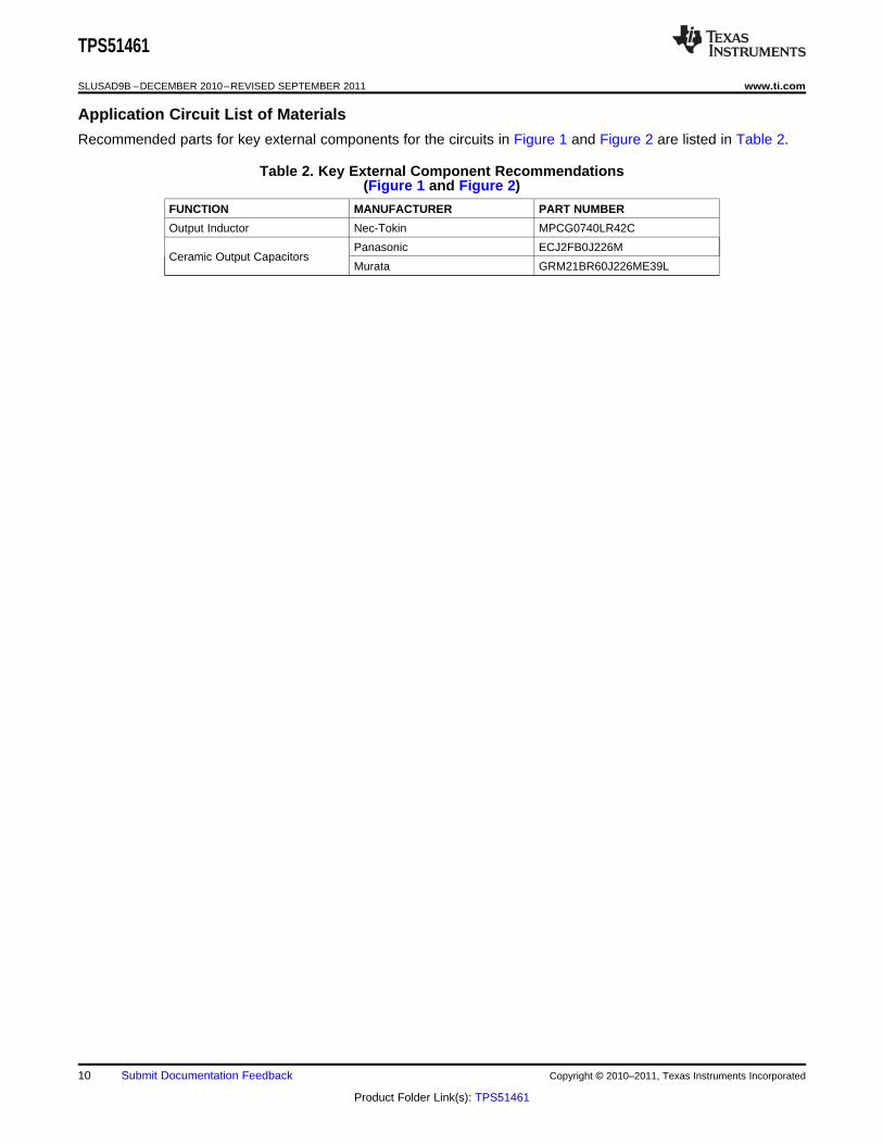
Application Circuit List of Materials
Recommended parts for key external components for the circuits in Figure 1 and Figure 2 are listed in Table 2.
Table 2. Key External Component Recommendations(Figure 1 and Figure 2)
FUNCTION MANUFACTURER PART NUMBER
Output Inductor Nec-Tokin MPCG0740LR42C
Panasonic ECJ2FB0J226MCeramic Output Capacitors
Murata GRM21BR60J226ME39L
10 Submit Documentation Feedback Copyright © 2010–2011, Texas Instruments Incorporated
Product Folder Link(s): TPS51461

Time (ms)
Vo
ltag
e(V
)
Current
Feedback
tON
t
VCS
VCOMP
UDG-10187
VREF
TPS51461
www.ti.com SLUSAD9B –DECEMBER 2010–REVISED SEPTEMBER 2011
APPLICATION INFORMATION
Functional Overview
The TPS51461 is a D-CAP+™ mode adaptive on-time converter. The output voltage is set using a 2-bit DAC thatoutputs a reference voltage in accordance with the code defined in Table 1. VID-on-the-fly transitions aresupported with the slew rate controlled by a single capacitor on the SLEW pin. Integrated high-side and low-sideFET supports output current to a maximum of 6-ADC. The converter automatically runs in discontinuousconduction mode (DCM) to optimize light-load efficiency. Two switching frequency selections are provided, (700kHz and 1 MHz) to enable optimization of the power chain for the cost, size and efficiency requirements of thedesign.
In adaptive on-time converters, the controller varies the on-time as a function of input and output voltage tomaintain a nearly constant frequency during steady-state conditions. In conventional constant on-time converters,each cycle begins when the output voltage crosses to a fixed reference level. However, in the TPS51461, thecycle begins when the current feedback reaches an error voltage level which is the amplified difference betweenthe reference voltage and the feedback voltage.
PWM Operation
Referring to Figure 3, in steady state, continuous conduction mode, the converter operates in the following way.
Starting with the condition that the top FET is off and the bottom FET is on, the current feedback (VCS) is higherthan the error amplifier output (VCOMP). VCS falls until it hits VCOMP, which contains a component of the outputripple voltage. VCS is not directly accessible by measuring signals on pins of TPS51461. The PWM comparatorsenses where the two waveforms cross and triggers the on-time generator.
Figure 3. D-CAP+™ Mode Basic Waveforms
The current feedback is an amplified and filtered version of the voltage between PGND and SW during low-sideFET on-time. The TPS51461 also provides a single-ended differential voltage (VOUT) feedback to increase thesystem accuracy and reduce the dependence of circuit performance on layout.
Copyright © 2010–2011, Texas Instruments Incorporated Submit Documentation Feedback 11
Product Folder Link(s): TPS51461

= ´OUT
ON
IN SW
V 1t
V f
+V
SLEW
+
–
RC
+ PWM
Comparator
RDS(on)
GMV
= 1 mS
Driver
LOUT
ESR
COUT
ROUT
UDG-10190
RLOAD
8 kW
+
–
+G
MC= 1 mS
CC
VREF
TPS51461
SLUSAD9B –DECEMBER 2010–REVISED SEPTEMBER 2011 www.ti.com
PWM Frequency and Adaptive on Time Control
In general, the on-time (at the SW node) can be estimated byEquation 1.
where• fSW is the frequency selected by the connection of the MODE pin (1)
The on-time pulse is sent to the top FET. The inductor current and the current feedback rises to peak value.Each ON pulse is latched to prevent double pulsing. Switching frequency settings are shown in Table 3.
Non-Droop Configuration
The TPS51461 can be configured as a non-droop solution. The benefit of a non-droop approach is that loadregulation is flat, therefore, in a system where tight DC tolerance is desired, the non-droop approach isrecommended. For the Intel system agent application, non-droop is recommended as the standard configuration.
The non-droop approach can be implemented by connecting a resistor and a capacitor between the COMP andthe VREF pins. The purpose of the type II compensation is to obtain high DC feedback gain while minimizing thephase delay at unity gain cross over frequency of the converter.
The value of the resistor (RC) can be calculated using the desired unity gain bandwidth of the converter, and thevalue of the capacitor (CC) can be calculated by knowing where the zero location is desired. An application toolthat calculates these values is available from your local TI Field Application Engineer.
Figure 4 shows the basic implementation of the non-droop mode using the TPS51461.
Figure 4. Non-Droop Mode Basic Implementation
Figure 5 shows the load regulation of the system agent rail using non-droop configuration.
Figure 6 shows the transient response of TPS51461 using non-droop configuration where COUT = 4 × 22 µF. Theapplied step load is from 0 A to 2 A.
12 Submit Documentation Feedback Copyright © 2010–2011, Texas Instruments Incorporated
Product Folder Link(s): TPS51461

0.73
0.75
0.77
0.79
0.81
0.83
0.85
0.87
0 1 2 3 4 5 6Output Current (A)
Out
put V
olta
ge (
V)
Mode 3Mode 4Mode 7Mode 8 VIN = 5 V
´=
´
CSINTDROOP
DROOP M
A I(L)V
R G
= = \ =´ ´
DROOP CSINT CSINTLOAD _LINE DROOP
DROOP M LOAD _LINE M
V A AR R
I(L) R G R G
TPS51461
www.ti.com SLUSAD9B –DECEMBER 2010–REVISED SEPTEMBER 2011
Figure 5. 0.8-V Load Regulation (VIN = 5 V) Figure 6. Non-Droop Configuration TransientNon-Droop Configuration Response
Droop Configuration
The terminology for droop is the same as load line or voltage positioning as defined in the Intel CPU VCOREspecification. Based on the actual tolerance requirement of the application, load-line set points can be defined tomaximize either cost savings (by reducing output capacitors) or power reduction benefits.
Accurate droop voltage response is provided by the finite gain of the droop amplifier. The equation for droopvoltage is shown in Equation 2.
where• low-side on-resistence is used as the current sensing element• ACSINT is a constant, which nominally is 53 mV/A.• I(L) is the DC current of the inductor, or the load current• RDROOP is the value of resistor from the COMP pin to the VREF pin• GM is the transconductance of the droop amplifier with nominal value of 1 mS (2)
(3)
Therefore, if a 5-mΩ load line to the system agent rail is desired, the calculated RDROOP is approximately 10 kΩ.Equation 2 can be used to easily derive RDROOP for any load line slope/droop design target.
Copyright © 2010–2011, Texas Instruments Incorporated Submit Documentation Feedback 13
Product Folder Link(s): TPS51461

+V
SLEW
+
–
RDROOP
+ PWM
Comparator
RDS(on)
GMV
= 1 mS
Driver
LOUT
ESR
COUT
ROUT
UDG-10188
RLOAD
8 kW
+
–
+G
MC= 1 mS
VREF
UDG-10189
Droop
ILOAD
VOUT
setpoint at 0 A
Maximum undershoot voltage =(5%–1%) x 1 = 4% x VOUT
Lead insertion
Lead release
Non-
Droop
Maximum transient voltage
= (5%–1%) x 2 = 8% x VOUT
VOUT
setpoint at 6 A
VOUT
setpoint at 0 A
Maximum overshoot voltage =(5%–1%) x 1 = 4% x VOUT
TPS51461
SLUSAD9B –DECEMBER 2010–REVISED SEPTEMBER 2011 www.ti.com
Figure 7 shows the basic implementation of the droop mode using the TPS51461.
Figure 7. DROOP Mode Basic Implementation
The droop (voltage positioning) method was originally recommended to reduce the number of external outputcapacitors required. The effective transient voltage range is increased because of the active voltage positioning(see Figure 8).
Figure 8. DROOP vs Non-DROOP in Transient Voltage Window
14 Submit Documentation Feedback Copyright © 2010–2011, Texas Instruments Incorporated
Product Folder Link(s): TPS51461

0.75
0.76
0.77
0.78
0.79
0.80
0.81
0.82
0.83
0.84
0 1 2 3 4 5 6Output Current (A)
Out
put V
olta
ge (
V)
VIN = 3.3 V
TPS51461
www.ti.com SLUSAD9B –DECEMBER 2010–REVISED SEPTEMBER 2011
Consider an example of 0.8 V ±5%. If no droop is permitted, the allowable transient overshoot can be at amaximum of +4%; the allowed transient undershoot can only be at minimum of –4% (given a dc tolerance of±1%). Therefore, the overshoot and undershoot window is only ±32 mV. If the droop method is applied, thisovershoot and undershoot window could be potentially doubled from ±32 mV to ±64 mV, given the same loadstep and release.
In applications where the DC and the AC tolerances are not separated, which means there is not a strict DCtolerance requirement, the droop method can be used.
Table 3. Mode Parameter Table
COMPENSATIONSWITCHING VID1 = 1TECHNOLOGYMODEMODE VREF (V) FREQUENCY VID0 = 0CONNECTION NON- (fSW) (V)DROOP DROOP
1 GND X 2.06 1 MHz 0.80
3 22 kΩ X X 2.01 700 kHz 0.80
4 33 kΩ X X 2.01 1 MHz 0.85
5 47 kΩ X 2.06 1 MHz 0.85
7 100 kΩ X X 2.01 700 kHz 0.85
8 Open X X 2.01 1 MHz 0.80
Figure 9 shows the load regulation of the 0.8-V rail using an RDROOP value of 10 kΩ.
Figure 10 shows the transient response of the TPS51461 using droop configuration and COUT = 4 × 22 µF. Theapplied step load is from 0 A to 2 A.
Figure 9. 0.8-V Load Regulation (VIN = 3.3 V) Figure 10. Droop Configuration TransientResponse
Copyright © 2010–2011, Texas Instruments Incorporated Submit Documentation Feedback 15
Product Folder Link(s): TPS51461

=SLEW
SLEW
IC
SR
´= SLEW
SS
SLEW
C 0.9 Vt
I
TPS51461
SLUSAD9B –DECEMBER 2010–REVISED SEPTEMBER 2011 www.ti.com
Light Load Power Saving Features
The TPS51461 has an automatic pulse-skipping mode to provide excellent efficiency over a wide load range.The converter senses inductor current and prevents negative flow by shutting off the low-side gate driver. Thissaves power by eliminating re-circulation of the inductor current. Further, when the bottom FET shuts off, theconverter enters discontinuous mode, and the switching frequency decreases, thus reducing switching losses aswell.
Voltage Slewing
The TPS51461 ramps the SLEW voltage up and down to perform the output voltage transitioning. The timing isindependent of switching frequency, as well as output resistive and capacitive loading. It is set by a capacitorfrom SLEW pin to GND, called CSLEW, together with an internal current source of 10 µA. The slew rate is used toset the startup and voltage transition rate.
(4)
where• ISLEW = 10 µA (nom)• SR is the target output voltage slew rate, per Intel specification between 0.5 mV/µs and 10 mV/µs (5)
For the current reference design, an SR of 1 mV/µs is targeted. The CSLEW is calculated to be 10 nF. The slowerslew rate is desired to minimize large inductor current perturbation during startup and voltage transitioning thusreducing the possibility of acoustic noise.
After the power up, when VID1 is transitioning from 0 to 1, TPS51461 follows the SLEW voltage entering theforced PWM mode to actively discharge the output voltage from 0.9 V to 0.8 V. The actual output voltage slewrate is approximately the same as the set slew rate while the bandwidth of the converter supports it and there isno overcurrent triggered by additional charging current flowing into the output capacitors. After SLEW transition iscompleted, PWM mode is maintained for 64 µs (16 clock cycles when the frequency is 1 MHz) to ensure voltageregulation.
Protection Features
The TPS51461 offers many features to protect the converter power chain as well as the system electronics.
5-V Undervoltage Protection (UVLO)
The TPS51461 continuously monitors the voltage on the V5FILT pin to ensure that the voltage level is highenough to bias the device properly and to provide sufficient gate drive potential to maintain high efficiency. Theconverter starts with approximately 4.3 V and has a nominal of 440 mV of hysteresis. If the 5-V UVLO limit isreached, the converter transitions the phase node into a 3-state function. And the converter remains in the offstate until the device is reset by cycling 5 V until the 5-V POR is reached (2.3-V nominal). The power input doesnot have an UVLO function
Power Good Signals
The TPS51461 has one open-drain power good (PGOOD) pin. During startup, there is a 3 ms power good delaystarting from the output voltage reaching the regulation point (excluding soft-start ramp-up time). And there isalso a 1 ms power good high propagation delay. The PGOOD pin de-asserts as soon as the EN pin is pulled lowor an undervoltage condition on V5FILT is detected. The PGOOD signal is blanked during VID voltage transitionsto prevent false triggering during voltage slewing.
16 Submit Documentation Feedback Copyright © 2010–2011, Texas Instruments Incorporated
Product Folder Link(s): TPS51461

( ) ( ) -= + ´ P POCL dc OCL valley
1I I I
2
TPS51461
www.ti.com SLUSAD9B –DECEMBER 2010–REVISED SEPTEMBER 2011
Output Overvoltage Protection (OVP)
In addition to the power good function described above, the TPS51461 has additional OVP and UVP thresholdsand protection circuits.
An OVP condition is detected when the output voltage is approximately 120% × VSLEW. In this case, theconverter de-asserts the PGOOD signals and performs the overvoltage protection function. The converterremains in this state until the device is reset by cycling 5 V until the 5-V POR threshold (2.3 V nominal) isreached.
Output Undervoltage Protection (UVP)
Output undervoltage protection works in conjunction with the current protection described in the OvercurrentProtection and Overcurrent Limit sections. If the output voltage drops below 70% of VSLEW, after an 8-µs delay,the device latches OFF. Undervoltage protection can be reset only by EN or a 5-V POR.
Overcurrent Protection
Both positive and negative overcurrent protection are provided in the TPS51461:• Overcurrent Limit (OCL)• Negative OCL (level same as positive OCL)
Overcurrent Limit
If the sensed current value is above the OCL setting, the converter delays the next ON pulse until the currentdrops below the OCL limit. Current limiting occurs on a pulse-by-pulse basis. The TPS51461 uses a valleycurrent limiting scheme where the DC OCL trip point is the OCL limit plus half of the inductor ripple current. Theminimum valley OCL is 6 A over process and temperature.
During the overcurrent protection event, the output voltage likely droops until the UVP limit is reached. Then, theconverter de-asserts the PGOOD pin, and then latches OFF after an 8-µs delay. The converter remains in thisstate until the device is reset by EN or a 5VFILT POR.
(6)
Negative OCL
The negative OCL circuit acts when the converter is sinking current from the output capacitor(s). The convertercontinues to act in a valley mode, the absolute value of the negative OCL set point is typically -6.5 A.
Thermal Protection
Thermal Shutdown
The TPS51461 has an internal temperature sensor. When the temperature reaches a nominal 130°C, the deviceshuts down until the temperature cools by approximately 10°C. Then the converter restarts.
Copyright © 2010–2011, Texas Instruments Incorporated Submit Documentation Feedback 17
Product Folder Link(s): TPS51461
VCCP0.95 V
1.05-V Rail
260 ms
EN
Internal Enable
VID1 (3)
VID0 (3)
SLEW (1 mV/ms)
VOUT
VCCSA_PGOOD
UNCORE_PWRGD (1)
900 ms 4 ms 2.5 ms
Reset Time (2)
UDG-10191
TPS51461
SLUSAD9B –DECEMBER 2010–REVISED SEPTEMBER 2011 www.ti.com
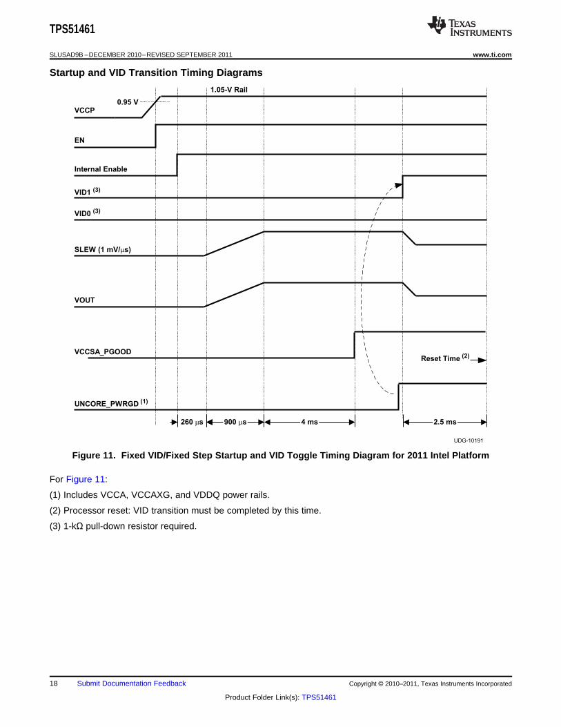
Startup and VID Transition Timing Diagrams
Figure 11. Fixed VID/Fixed Step Startup and VID Toggle Timing Diagram for 2011 Intel Platform
For Figure 11:
(1) Includes VCCA, VCCAXG, and VDDQ power rails.
(2) Processor reset: VID transition must be completed by this time.
(3) 1-kΩ pull-down resistor required.
18 Submit Documentation Feedback Copyright © 2010–2011, Texas Instruments Incorporated
Product Folder Link(s): TPS51461

VCCP0.95 V
1.05-V Rail
260 ms
EN
Internal Enable
VID1 (3)
VID0 (3)
SLEW (1 mV/ms)
VOUT
VCCSA_PGOOD
UNCORE_PWRGD (1)
900 ms 4 ms 2.5 ms
Reset Time (2)
UDG-10192
100ms
TPS51461
www.ti.com SLUSAD9B –DECEMBER 2010–REVISED SEPTEMBER 2011
Figure 12. Fixed VID/Fixed Step Startup and VID Toggle Timing Diagram for 2012 Intel Platform
For Figure 12:
(1) Includes VCCA, VCCAXG, and VDDQ power rails.
(2) Processor reset: VID transition must be completed by this time.
(3) 1-kΩ pull-down resistor required.
Copyright © 2010–2011, Texas Instruments Incorporated Submit Documentation Feedback 19
Product Folder Link(s): TPS51461

40
45
50
55
60
65
70
75
80
85
90
0.01 0.1 1 10Output Current (A)
Effi
cien
cy (
%)
Mode 1Mode 3Mode 4Mode 7Mode 8
TA = 25°CVIN = 3.3 V
40
45
50
55
60
65
70
75
80
85
90
0.01 0.1 1 10Output Current (A)
Effi
cien
cy (
%)
Mode 1Mode 3Mode 4Mode 7Mode 8
TA = 25°CVIN = 5 V
0.00
0.25
0.50
0.75
1.00
1.25
0.1 1 10Output Current (A)
Pow
er L
oss
(W)
Mode 1Mode 3Mode 4Mode 7Mode 8
TA = 25°CVIN = 3.3 V
0.00
0.25
0.50
0.75
1.00
1.25
0.1 1 10Output Current (A)
Pow
er L
oss
(W)
Mode 1Mode 3Mode 4Mode 7Mode 8
TA = 25°CVIN = 5 V
100
150
200
250
300
350
400
50
0
-30
-20
-10
30
40
50
-40
-50
0
10
20
Frequency (Hz)
Gain
Phase
1000 10 k 100 k 1 M 10 M
Gain
(dB
)
Phase
(°)
25°C
-10°C
85°C
60
110
160
210
260
310
360
10
-40
-30
-20
-10
30
40
50
-40
-50
0
10
20
Frequency (Hz)
Gain
Phase
25°C
-10°C
85°C
1000 10 k 100 k 1 M 10 M
Gain
(dB
)
Phase
(°)
60
TPS51461
SLUSAD9B –DECEMBER 2010–REVISED SEPTEMBER 2011 www.ti.com
TYPICAL CHARACTERISTICS
Figure 13. Efficiency vs Output Current Figure 14. Efficiency vs Output Current
Figure 15. Power Loss Figure 16. Power Loss
Figure 17. Bode Plot (Non-Droop Mode) VIN = 5 V, Figure 18. Bode Plot (Droop Mode), VIN = 5 V,VOUT = 0.8 V, ILOAD = 5 A VOUT = 0.8 V, ILOAD = 5 A
20 Submit Documentation Feedback Copyright © 2010–2011, Texas Instruments Incorporated
Product Folder Link(s): TPS51461

TPS51461
www.ti.com SLUSAD9B –DECEMBER 2010–REVISED SEPTEMBER 2011
TYPICAL CHARACTERISTICS (continued)
Figure 19. Mode 8 Non-Droop, 0 A Figure 20. Mode 8 Non-Droop, 3 A
Figure 21. Mode 8 Droop, 0 A Figure 22. Mode 8 Droop, 3 A
Figure 23. Mode 4 Non-Droop 0 A Figure 24. Mode 4 Non-Droop 3 A
Copyright © 2010–2011, Texas Instruments Incorporated Submit Documentation Feedback 21
Product Folder Link(s): TPS51461

TPS51461
SLUSAD9B –DECEMBER 2010–REVISED SEPTEMBER 2011 www.ti.com
TYPICAL CHARACTERISTICS (continued)
Figure 25. Mode 4 Droop 0 A Figure 26. Mode 4 Droop 3 A
22 Submit Documentation Feedback Copyright © 2010–2011, Texas Instruments Incorporated
Product Folder Link(s): TPS51461

- = ´ =P PI 6 A 0.25 1.5 A
( )( )
( )( )
- -
æ ö æ ö- ´ - ´ç ÷ ç ÷
ç ÷ ç ÷´ ´´ è ø è ø= = = = m
10IN 10
SW IN
P P P P
V 0.8V V 5 0.8
f V 1 5V dTL 0.45 H
I I 1.5 A
m= = =
m
SLEWSLEW
DAC
I 10 AC 10nF
1mVSRs
TPS51461
www.ti.com SLUSAD9B –DECEMBER 2010–REVISED SEPTEMBER 2011
DESIGN PROCEDURE
The simplified design procedure is done for a non-droop application using the TPS51461 converter.
Step One
Determine the specifications.
The System Agent Rail requirements provide the following key parameters:1. V00 = 0.90 V2. V10 = 0.80 V3. ICC(max) = 6 A4. IDYN(max) = 2 A5. ICC(tdc) = 3 A
Step Two
Determine system parameters.
The input voltage range and operating frequency are of primary interest. For example:1. VIN = 5 V2. fSW = 1 MHz
Step Three
Determine inductor value and choose inductor.
Smaller values of inductor have better transient performance but higher ripple and lower efficiency. Higher valueshave the opposite characteristics. It is common practice to limit the ripple current to 25% to 50% of the maximumcurrent. In this case, use 25%:
(7)
At fSW = 1 MHz, with a 5-V input and a 0.80-V output:
(8)
For this application, a 0.42-µH, 1.55-mΩ inductor from NEC-TOKIN with part number MPCG0740LR42C ischosen.
Step Four
Set the output voltage.
The output voltage is determined by the VID settings. The actual voltage set point for each VID setting is listed inTable 1. No external resistor dividers are needed for this design.
Step Five
Calculate CSLEW.
VID pin transition and soft-start time is determined by CSLEW and 10 µA of internal current source.
(9)
The slower slew rate is desired to minimize large inductor current perturbation during startup and voltagetransition, thus reducing the possibility of acoustic noise.
Copyright © 2010–2011, Texas Instruments Incorporated Submit Documentation Feedback 23
Product Folder Link(s): TPS51461

´ ´= = = m
m
SLEWSS
SLEW
C 0.9 V 10nF 0.9 Vt 900 s
I 10 A
( ) ( ) -= + ´ = + ´ =P POCL dc OCL valley
1 1I I I 6 A 1.5 A 6.75 A
2 2
( )
( )( )
( )
( )
( )
( )( )
æ ö´
ç ÷´ D ´ +ç ÷è ø
=æ öæ ö-ç ÷ç ÷´ D ´ ´ - ´ç ÷ç ÷è øè ø
2 VOUT SWLOAD max MIN off
IN min
OUT min_under
VOUTIN min
SW VOUTLOAD insert MIN off
IN min
V tL I t
V
C
V V
2 V t t VV
( )( )( )
( )
´ D
=´ D ´
2
OUT LOAD max
OUT min_ overVOUTLOAD release
L I
C2 V V
TPS51461
SLUSAD9B –DECEMBER 2010–REVISED SEPTEMBER 2011 www.ti.com
Given the CSLEW, use Equation 10 to calculate the soft start time.
(10)
Step Six
Calculate OCL.
The DC OCL level of TPS51461 design is determined by Equation 11,
(11)
The minimum valley OCL is 6 A over process and temperature, and IP-P = 1.5 A, the minimum DC OCL iscalculated to be 6.75A.
Step Seven
Determine the output capacitance.
To determine COUT based on transient and stability requirement, first calculate the the minimum outputcapacitance for a given transient.
Equation 13 and Equation 12 can be used to estimate the amount of capacitance needed for a given dynamicload step/release. Please note that there are other factors that may impact the amount of output capacitance fora specific design, such as ripple and stability. Equation 13 and Equation 12 are used only to estimate thetransient requirement, the result should be used in conjunction with other factors of the design to determine thenecessary output capacitance for the application.
(12)
(13)
Equation 12 and Equation 13 calculate the minimum COUT for meeting the transient requirement, which is72.9 µF assuming the following:• ±3% voltage allowance for load step and release• MLCC capacitance derating of 60% due to DC and AC bias effect
In this reference design, 4, 22-µF capacitors are used in order to provide this amount of capacitance.
24 Submit Documentation Feedback Copyright © 2010–2011, Texas Instruments Incorporated
Product Folder Link(s): TPS51461

= ´ ´ =p
CM0
OUT S
RG1f 150kHz
2 C R
´ ´ p ´ ´ W ´ p ´ m= = » W
0 S OUTC
M
f R 2 C 150kHz 53m 2 88 FR 5k
G 1mS
=p ´ ´
=0
Z
C C
f1f
2 R C 10
TPS51461
www.ti.com SLUSAD9B –DECEMBER 2010–REVISED SEPTEMBER 2011
Step Eight
Determine the stability based on the output capacitance COUT.
In order to achieve stable operation. The 0-dB frequency, f0 should be kept less than 1/5 of the switchingfrequency (1 MHz). (See Figure 4)
where• RS = RDS(on) × GMC × RLOAD (14)
.
(15)
Using 4, 22-µF capacitors, the compensation resistance, RC can be calculated to be approximately 5 kΩ.
The purpose of the comparator capacitor (CC) is to reduce the DC component to obtain high DC feedback gain.However, as it causes phase delay, another zero to cancel this effect at f0 is needed. This zero can bedetermined by values of CC and the compensation resistor, RC.
(16)
And since RC has previously been derived, the value of CC is calculated to be 2.2 nF. In order to further boostphase margin, a value of 3.3-nF is chosen for this reference design.
Step Nine
Select decoupling and peripheral components.
For TPS51461 peripheral capacitors use the following minimum values of ceramic capacitance. X5R or bettertemperature coefficient is recommended. Tighter tolerances and higher voltage ratings are always appropriate.• V5DRV decoupling ≥ 2.2 µF, ≥ 10 V• V5FILT decoupling ≥ 1 µF, ≥10 V• VREF decoupling 0.22 µF to 1 µF, ≥ 4 V• Bootstrap capacitors ≥ 0.1 µF, ≥ 10 V• Pull-up resistors on PGOOD, 100 kΩ
Layout Considerations
Good layout is essential for stable power supply operation. Follow these guidelines for an efficient PCB layout.• Connect PGND pins (or at least one of the pins) to the thermal PAD underneath the device. Also connect
GND pin to the thermal PAD underneath the device. Use four vias to connect the thermal pad to internalground planes.
• Place VIN, V5DRV, V5FILT and 2VREF decoupling capacitors as close to the device as possible.• Use wide traces for the VIN, VOUT, PGND and SW pins. These nodes carry high current and also serve as
heat sinks.• Place feedback and compensation components as close to the device as possible.• Keep analog signals (SLEW, COMP) away from noisy signals (SW, VBST).
Copyright © 2010–2011, Texas Instruments Incorporated Submit Documentation Feedback 25
Product Folder Link(s): TPS51461

TPS51461
SLUSAD9B –DECEMBER 2010–REVISED SEPTEMBER 2011 www.ti.com
Changes from Revision A (DECEMBER 2010) to Revision B Page
• Changed title in Figure 1 to "Droop Configuration". .............................................................................................................. 8
• Changed title in Figure 2 to "Non-Droop Configuration". ...................................................................................................... 9
26 Submit Documentation Feedback Copyright © 2010–2011, Texas Instruments Incorporated
Product Folder Link(s): TPS51461

PACKAGE OPTION ADDENDUM
www.ti.com 11-Apr-2013
Addendum-Page 1
PACKAGING INFORMATION
Orderable Device Status(1)
Package Type PackageDrawing
Pins PackageQty
Eco Plan(2)
Lead/Ball Finish MSL Peak Temp(3)
Op Temp (°C) Top-Side Markings(4)
Samples
TPS51461RGER ACTIVE VQFN RGE 24 3000 Green (RoHS& no Sb/Br)
CU NIPDAU Level-2-260C-1 YEAR -40 to 85 TPS51461
TPS51461RGET ACTIVE VQFN RGE 24 250 Green (RoHS& no Sb/Br)
CU NIPDAU Level-2-260C-1 YEAR -40 to 85 TPS51461
(1) The marketing status values are defined as follows:ACTIVE: Product device recommended for new designs.LIFEBUY: TI has announced that the device will be discontinued, and a lifetime-buy period is in effect.NRND: Not recommended for new designs. Device is in production to support existing customers, but TI does not recommend using this part in a new design.PREVIEW: Device has been announced but is not in production. Samples may or may not be available.OBSOLETE: TI has discontinued the production of the device.
(2) Eco Plan - The planned eco-friendly classification: Pb-Free (RoHS), Pb-Free (RoHS Exempt), or Green (RoHS & no Sb/Br) - please check http://www.ti.com/productcontent for the latest availabilityinformation and additional product content details.TBD: The Pb-Free/Green conversion plan has not been defined.Pb-Free (RoHS): TI's terms "Lead-Free" or "Pb-Free" mean semiconductor products that are compatible with the current RoHS requirements for all 6 substances, including the requirement thatlead not exceed 0.1% by weight in homogeneous materials. Where designed to be soldered at high temperatures, TI Pb-Free products are suitable for use in specified lead-free processes.Pb-Free (RoHS Exempt): This component has a RoHS exemption for either 1) lead-based flip-chip solder bumps used between the die and package, or 2) lead-based die adhesive used betweenthe die and leadframe. The component is otherwise considered Pb-Free (RoHS compatible) as defined above.Green (RoHS & no Sb/Br): TI defines "Green" to mean Pb-Free (RoHS compatible), and free of Bromine (Br) and Antimony (Sb) based flame retardants (Br or Sb do not exceed 0.1% by weightin homogeneous material)
(3) MSL, Peak Temp. -- The Moisture Sensitivity Level rating according to the JEDEC industry standard classifications, and peak solder temperature.
(4) Multiple Top-Side Markings will be inside parentheses. Only one Top-Side Marking contained in parentheses and separated by a "~" will appear on a device. If a line is indented then it is acontinuation of the previous line and the two combined represent the entire Top-Side Marking for that device.
Important Information and Disclaimer:The information provided on this page represents TI's knowledge and belief as of the date that it is provided. TI bases its knowledge and belief on informationprovided by third parties, and makes no representation or warranty as to the accuracy of such information. Efforts are underway to better integrate information from third parties. TI has taken andcontinues to take reasonable steps to provide representative and accurate information but may not have conducted destructive testing or chemical analysis on incoming materials and chemicals.TI and TI suppliers consider certain information to be proprietary, and thus CAS numbers and other limited information may not be available for release.
In no event shall TI's liability arising out of such information exceed the total purchase price of the TI part(s) at issue in this document sold by TI to Customer on an annual basis.

TAPE AND REEL INFORMATION
*All dimensions are nominal
Device PackageType
PackageDrawing
Pins SPQ ReelDiameter
(mm)
ReelWidth
W1 (mm)
A0(mm)
B0(mm)
K0(mm)
P1(mm)
W(mm)
Pin1Quadrant
TPS51461RGER VQFN RGE 24 3000 330.0 12.4 4.35 4.35 1.1 8.0 12.0 Q2
TPS51461RGER VQFN RGE 24 3000 330.0 12.4 4.25 4.25 1.15 8.0 12.0 Q2
TPS51461RGET VQFN RGE 24 250 180.0 12.4 4.25 4.25 1.15 8.0 12.0 Q2
TPS51461RGET VQFN RGE 24 250 180.0 12.5 4.35 4.35 1.1 8.0 12.0 Q2
PACKAGE MATERIALS INFORMATION
www.ti.com 23-Sep-2014
Pack Materials-Page 1

*All dimensions are nominal
Device Package Type Package Drawing Pins SPQ Length (mm) Width (mm) Height (mm)
TPS51461RGER VQFN RGE 24 3000 338.0 355.0 50.0
TPS51461RGER VQFN RGE 24 3000 367.0 367.0 35.0
TPS51461RGET VQFN RGE 24 250 210.0 185.0 35.0
TPS51461RGET VQFN RGE 24 250 338.0 355.0 50.0
PACKAGE MATERIALS INFORMATION
www.ti.com 23-Sep-2014
Pack Materials-Page 2

GENERIC PACKAGE VIEW
Images above are just a representation of the package family, actual package may vary.Refer to the product data sheet for package details.
RGE 24 VQFN - 1 mm max heightPLASTIC QUAD FLATPACK - NO LEAD
4204104/H


IMPORTANT NOTICE
Texas Instruments Incorporated (TI) reserves the right to make corrections, enhancements, improvements and other changes to itssemiconductor products and services per JESD46, latest issue, and to discontinue any product or service per JESD48, latest issue. Buyersshould obtain the latest relevant information before placing orders and should verify that such information is current and complete.TI’s published terms of sale for semiconductor products (http://www.ti.com/sc/docs/stdterms.htm) apply to the sale of packaged integratedcircuit products that TI has qualified and released to market. Additional terms may apply to the use or sale of other types of TI products andservices.Reproduction of significant portions of TI information in TI data sheets is permissible only if reproduction is without alteration and isaccompanied by all associated warranties, conditions, limitations, and notices. TI is not responsible or liable for such reproduceddocumentation. Information of third parties may be subject to additional restrictions. Resale of TI products or services with statementsdifferent from or beyond the parameters stated by TI for that product or service voids all express and any implied warranties for theassociated TI product or service and is an unfair and deceptive business practice. TI is not responsible or liable for any such statements.Buyers and others who are developing systems that incorporate TI products (collectively, “Designers”) understand and agree that Designersremain responsible for using their independent analysis, evaluation and judgment in designing their applications and that Designers havefull and exclusive responsibility to assure the safety of Designers' applications and compliance of their applications (and of all TI productsused in or for Designers’ applications) with all applicable regulations, laws and other applicable requirements. Designer represents that, withrespect to their applications, Designer has all the necessary expertise to create and implement safeguards that (1) anticipate dangerousconsequences of failures, (2) monitor failures and their consequences, and (3) lessen the likelihood of failures that might cause harm andtake appropriate actions. Designer agrees that prior to using or distributing any applications that include TI products, Designer willthoroughly test such applications and the functionality of such TI products as used in such applications.TI’s provision of technical, application or other design advice, quality characterization, reliability data or other services or information,including, but not limited to, reference designs and materials relating to evaluation modules, (collectively, “TI Resources”) are intended toassist designers who are developing applications that incorporate TI products; by downloading, accessing or using TI Resources in anyway, Designer (individually or, if Designer is acting on behalf of a company, Designer’s company) agrees to use any particular TI Resourcesolely for this purpose and subject to the terms of this Notice.TI’s provision of TI Resources does not expand or otherwise alter TI’s applicable published warranties or warranty disclaimers for TIproducts, and no additional obligations or liabilities arise from TI providing such TI Resources. TI reserves the right to make corrections,enhancements, improvements and other changes to its TI Resources. TI has not conducted any testing other than that specificallydescribed in the published documentation for a particular TI Resource.Designer is authorized to use, copy and modify any individual TI Resource only in connection with the development of applications thatinclude the TI product(s) identified in such TI Resource. NO OTHER LICENSE, EXPRESS OR IMPLIED, BY ESTOPPEL OR OTHERWISETO ANY OTHER TI INTELLECTUAL PROPERTY RIGHT, AND NO LICENSE TO ANY TECHNOLOGY OR INTELLECTUAL PROPERTYRIGHT OF TI OR ANY THIRD PARTY IS GRANTED HEREIN, including but not limited to any patent right, copyright, mask work right, orother intellectual property right relating to any combination, machine, or process in which TI products or services are used. Informationregarding or referencing third-party products or services does not constitute a license to use such products or services, or a warranty orendorsement thereof. Use of TI Resources may require a license from a third party under the patents or other intellectual property of thethird party, or a license from TI under the patents or other intellectual property of TI.TI RESOURCES ARE PROVIDED “AS IS” AND WITH ALL FAULTS. TI DISCLAIMS ALL OTHER WARRANTIES ORREPRESENTATIONS, EXPRESS OR IMPLIED, REGARDING RESOURCES OR USE THEREOF, INCLUDING BUT NOT LIMITED TOACCURACY OR COMPLETENESS, TITLE, ANY EPIDEMIC FAILURE WARRANTY AND ANY IMPLIED WARRANTIES OFMERCHANTABILITY, FITNESS FOR A PARTICULAR PURPOSE, AND NON-INFRINGEMENT OF ANY THIRD PARTY INTELLECTUALPROPERTY RIGHTS. TI SHALL NOT BE LIABLE FOR AND SHALL NOT DEFEND OR INDEMNIFY DESIGNER AGAINST ANY CLAIM,INCLUDING BUT NOT LIMITED TO ANY INFRINGEMENT CLAIM THAT RELATES TO OR IS BASED ON ANY COMBINATION OFPRODUCTS EVEN IF DESCRIBED IN TI RESOURCES OR OTHERWISE. IN NO EVENT SHALL TI BE LIABLE FOR ANY ACTUAL,DIRECT, SPECIAL, COLLATERAL, INDIRECT, PUNITIVE, INCIDENTAL, CONSEQUENTIAL OR EXEMPLARY DAMAGES INCONNECTION WITH OR ARISING OUT OF TI RESOURCES OR USE THEREOF, AND REGARDLESS OF WHETHER TI HAS BEENADVISED OF THE POSSIBILITY OF SUCH DAMAGES.Unless TI has explicitly designated an individual product as meeting the requirements of a particular industry standard (e.g., ISO/TS 16949and ISO 26262), TI is not responsible for any failure to meet such industry standard requirements.Where TI specifically promotes products as facilitating functional safety or as compliant with industry functional safety standards, suchproducts are intended to help enable customers to design and create their own applications that meet applicable functional safety standardsand requirements. Using products in an application does not by itself establish any safety features in the application. Designers mustensure compliance with safety-related requirements and standards applicable to their applications. Designer may not use any TI products inlife-critical medical equipment unless authorized officers of the parties have executed a special contract specifically governing such use.Life-critical medical equipment is medical equipment where failure of such equipment would cause serious bodily injury or death (e.g., lifesupport, pacemakers, defibrillators, heart pumps, neurostimulators, and implantables). Such equipment includes, without limitation, allmedical devices identified by the U.S. Food and Drug Administration as Class III devices and equivalent classifications outside the U.S.TI may expressly designate certain products as completing a particular qualification (e.g., Q100, Military Grade, or Enhanced Product).Designers agree that it has the necessary expertise to select the product with the appropriate qualification designation for their applicationsand that proper product selection is at Designers’ own risk. Designers are solely responsible for compliance with all legal and regulatoryrequirements in connection with such selection.Designer will fully indemnify TI and its representatives against any damages, costs, losses, and/or liabilities arising out of Designer’s non-compliance with the terms and provisions of this Notice.
Mailing Address: Texas Instruments, Post Office Box 655303, Dallas, Texas 75265Copyright © 2018, Texas Instruments Incorporated