Embed Size (px)
Citation preview
1
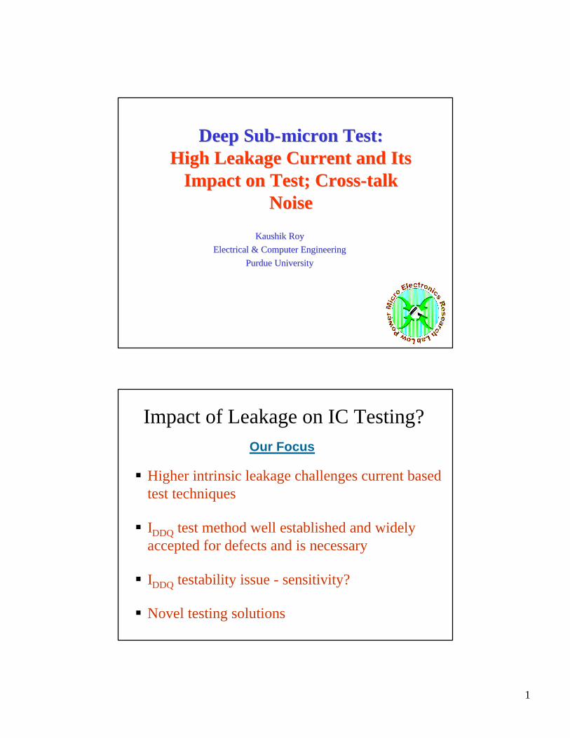
Deep SubDeep Sub--micron Test:micron Test:High Leakage Current and Its High Leakage Current and Its
Impact on Test; CrossImpact on Test; Cross--talk talk NoiseNoise
Kaushik RoyKaushik Roy
Electrical & Computer EngineeringElectrical & Computer Engineering
Purdue UniversityPurdue University
Impact of Leakage on IC Testing?
§ Higher intrinsic leakage challenges current based test techniques
§ IDDQ test method well established and widely accepted for defects and is necessary
§ IDDQ testability issue - sensitivity?
§ Novel testing solutions
Our Focus

2
Problem Statement
§ Can IDDQ and current based test methods be effective and survive the prohibitive increase in intrinsic leakage posed by technology scaling?
§ How do we discriminate high speed leaky ICs from defective ones?
n+ n+
Source
Gate
Drain
p-Well
I2 I3 I6
I7 I8
I4
I5 I1
Short Channel Transistor
Transistor Leakage Mechanisms

3
Components of IOFF
Leakage (IOFF) Current in Amps
1E-13
1E-9
1E-8
1E-7
1E-10
1E-11
1E-12pn junction
weak inversion + pn junction(80 mV/dec & VD = 0.1 V)
weak inversion + pn junction + DIBL@ VD = 2.7 V (VDD)
weak inversion + pn junction + DIBL + GIDL@ VD = 3.9 V (BI)
1. No punchthrough2. No width effect3. No gate leakage
For a 0.35 micron CMOS Technology
ð Subthreshold Leakage & SCE dominate
Weak inversion = subthreshold
IDDQ Testingü Measures current in power supply (VDD) during circuit
quiescent state (when all logic states have settled)
time
Vin
i DD
VDD
Vout
IDDQ StrobeDefect
No Defect (control) IDDQ
Vout
Vin
i DD
VSS
Defect
ð Choice of input vector matters in complex circuits

4
Gate Oxide Defect & IDDQ
ü IDDQ most effective in detecting defectsüExample: NMOS gate oxide defect creating a VDD to
VSS leakage path VDD
VSS
VDD
VSS
Gate oxide defect
0 1
ð Circuits become more susceptible to defects with scaling
Single Threshold IDDQ Test Limit
0
20
40
60
80
100
120
4.00
E-0
7
7.00
E-0
7
8.50
E-0
7
1.00
E-0
6
1.15
E-0
6
1.40
E-0
6
2.50
E-0
6
6.00
E-0
6
1.50
E-0
5
1.00
E-0
4
1.00
E-0
3
1.00
E-0
2
IDDQ (A)
Nu
mb
er o
f IC
s Limit
Limit Selection:1. Quality and Reliability2. Yield Loss and Cost
Failure Analysis to verify defectsand study outliers

5
µP IDDQ Distributions
ISB (mA)
99.9
99.599
95
90
80
7060504030
20
10
5
210.5
0.1
0 10 20 30 40 50 60 70 80
Cu
m D
ist (b)
(a)
Short Leff
Very Short Leff
(a)
(b)Normal Distribution
Limit ?
Limit concept on cumulative probability plots
Distribution Tail
Main Population
IDDQ
• Transient Current Testing [1,2]
• Current Signatures and Ratios [3,4]
• Delta IDDQ [5]
• Divide and conquer techniques [6,7]
• Forcing stacked transistors by input vector selection [8]
State-of-the-art in Current Testing
§ Not sufficient to address the problem§ Our solution not in conflict with above
6
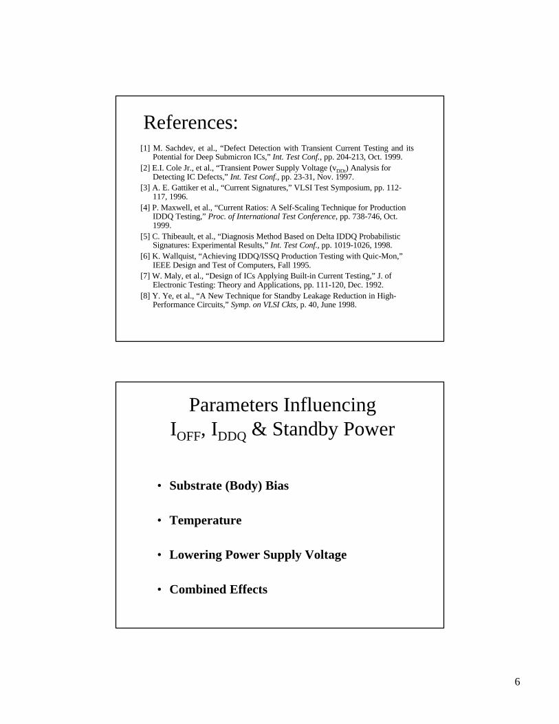
References: [1] M. Sachdev, et al., “Defect Detection with Transient Current Testing and its
Potential for Deep Submicron ICs,” Int. Test Conf., pp. 204-213, Oct. 1999.[2] E.I. Cole Jr., et al., “Transient Power Supply Voltage (vDDt) Analysis for
Detecting IC Defects,” Int. Test Conf., pp. 23-31, Nov. 1997.[3] A. E. Gattiker et al., “Current Signatures,” VLSI Test Symposium, pp. 112-
117, 1996.[4] P. Maxwell, et al., “Current Ratios: A Self-Scaling Technique for Production
IDDQ Testing,” Proc. of International Test Conference, pp. 738-746, Oct. 1999.
[5] C. Thibeault, et al., “Diagnosis Method Based on Delta IDDQ Probabilistic Signatures: Experimental Results,” Int. Test Conf., pp. 1019-1026, 1998.
[6] K. Wallquist, “Achieving IDDQ/ISSQ Production Testing with Quic-Mon,” IEEE Design and Test of Computers, Fall 1995.
[7] W. Maly, et al., “Design of ICs Applying Built-in Current Testing,” J. of Electronic Testing: Theory and Applications, pp. 111-120, Dec. 1992.
[8] Y. Ye, et al., “A New Technique for Standby Leakage Reduction in High-Performance Circuits,” Symp. on VLSI Ckts, p. 40, June 1998.
Parameters InfluencingIOFF, IDDQ & Standby Power
• Substrate (Body) Bias
• Temperature
• Lowering Power Supply Voltage
• Combined Effects

7
IOFF / Leakage Reductions
• Temperature– Factor of ~ 350 from room to -50°°C
• Substrate backbiasing (RBB) - VBS– Factor of ~ 3000 at ~ | 2 | V
• Lowered VDD– Factor of ~ 10 from 2.7 V to 1.5 V
• Multiple VT
For a 0.35 micron CMOS Technology
Two parameter Test Solution
• Scaling
• Functional and Delay Fault Testing
• IDDQ
• Components of transistor leakage
• Leakage reduction techniques
• Two-parameter test solution
• Sensitivity enhancement by RBB
• Sensitivity enhancement by Temperature

8
IDDQ tail? Fast or Defective ICs?
99.9
99.599
95
90
80
7060504030
20
10
5
210.5
0.1
0 10 20 30 40 50 60 70 80
ISB (mA)
Cu
m D
ist
(b)
(a)
Short Leff
Very Short Leff
(a)
(b)
Discriminate high speed ICs from defective ones
ð Intentionally skewed Leff shorter for higher performance
5% of the ICs are in the IDDQ distribution tail?
95%
IDDQ
IDDQ and FMAX as a function of Le
Normal Distribution
IDDQ =f(Lemin)
FMAX = f(Lemean)
LemeanLeminLe
# of
IC
s
Dominates leakage
Dictates performanceLe
ð Shorter channel transistors exponentially contribute more to IDDQ
1E-10
1E-09
1E-08
1E-07
1E-06
1E-05
1E-04
0.17 0.18 0.19 0.2 0.21 0.22 0.23 0.24
Leff (um) - Normalized
IOFF
(A)
IOFF
IOFF is an exponential function of Le.

9
IOFF Current and Le Distribution
Normal Distribution
IDDQ = f (Lemin)
FMAX = f (Lemean)
LemeanLemin Le
# of
IC
s
IOFF
Transistor Leakage Circuit Leakage
1
10
100
1000
10000
100000
0.1 1 10 100
Transistor Leakage - IOFF (nA)
IC L
eaka
ge
- ID
DQ
(u
A)
IOFF vs IDDQ
∑=
<n
iOFFDDQ i
II1

10
Two-Parameter Test Concept: Leakage vs Speed
FMAX
IDDQ
Defects
Upper Limit
FMAX vs IDDQ
Two-Parameter Test: Decision Table & Adjustable Limit
Table 6.1. IC decision matrix for IDDQ
and FMAX testing.
IDDQ FMAX Decision on IC
H H Good - Fast
H L Defect
L H Unlikely
L L Good - Slow

11
µP Circuit IDDQ vs FMAX
Normalized Maximum Frequency (FMAX)
No
rma
lize
d S
tati
c I SB I D
DQ IDDQ = f ( IOFF, VT, Le )
FMAX = f ( ID(SAT), VT, Le )
ð Empirical relationship derived from existing test methodsð Data include die-to-die parameter variation
Normalized Maximum Frequency (FMAX)
No
rmalize
d S
tati
c I
SB
IC leakier than expected for its speedDefective ?
Adjustable Limit Line
Trend Line
I D DQ
Adjustable Limit for IDDQ vs FMAX
ð Limit may be established by currently available statistical methods

12
Two-Parameter Test Practical Limitations
FMAX
IDDQ
Defects
Upper Limit
FMAX vs IDDQ
Thermal Runaway or Reliability Limit
Assumed leakage to frequency dependency
Adjustable Limit
Single Threshold Limit
Addressing issues raised by the problem statement
§ High intrinsic leakage§ Our solution places IDDQ in context of FMAX
§ High IDDQ leakage not an issue in itself§ High leakage at high speed is OK
§ IDDQ effectiveness and sensitivity§ Two-parameter test extends IDDQ effectiveness
§ More on improving sensitivity by RBB
§ Discriminates high speed leaky ICs from defective ones

13
§ No extra cost, no new hardware or instrumentation, uses established tests
§ It complements the existing methods such as lowering VDD, lowering temperature, and increasing VT by RBB or multiple VT
How does our solution compare to state-of-the-art in IDDQ testing?
Two-Parameter Test Leakage in context of Speed
FMAX
IDDQ
Defects
Upper Limit
FMAX vs IDDQ
Assumed leakage to frequency dependency
Adjustable Limit
Can we detect these defective ICs?
Detectable with Two-Parameter testing

14
Leakage Current & Power Measurements on an IC with 20,000 transistors
MU
XM
UX
FEM 95ChainChain
Delay Delay
ToggleFlipFlop
ToggleFlipFlop
Direct measurement of circuit leakage & delay:Delay tracks microprocessor clock frequency changein response to transistor performance change
Delay Chain and RO Circuits
IC Chip MeasurementsIC Chip Measurements
Improving the SensitivityTwo-Parameter Test + RBB and/or T
FMAX
IDDQ
Test & its limit after RBB or T
Original test & its limit
Detectable by RBB or T
Detectable with two-parameter testing
Defect threshold current
Don’t care defect
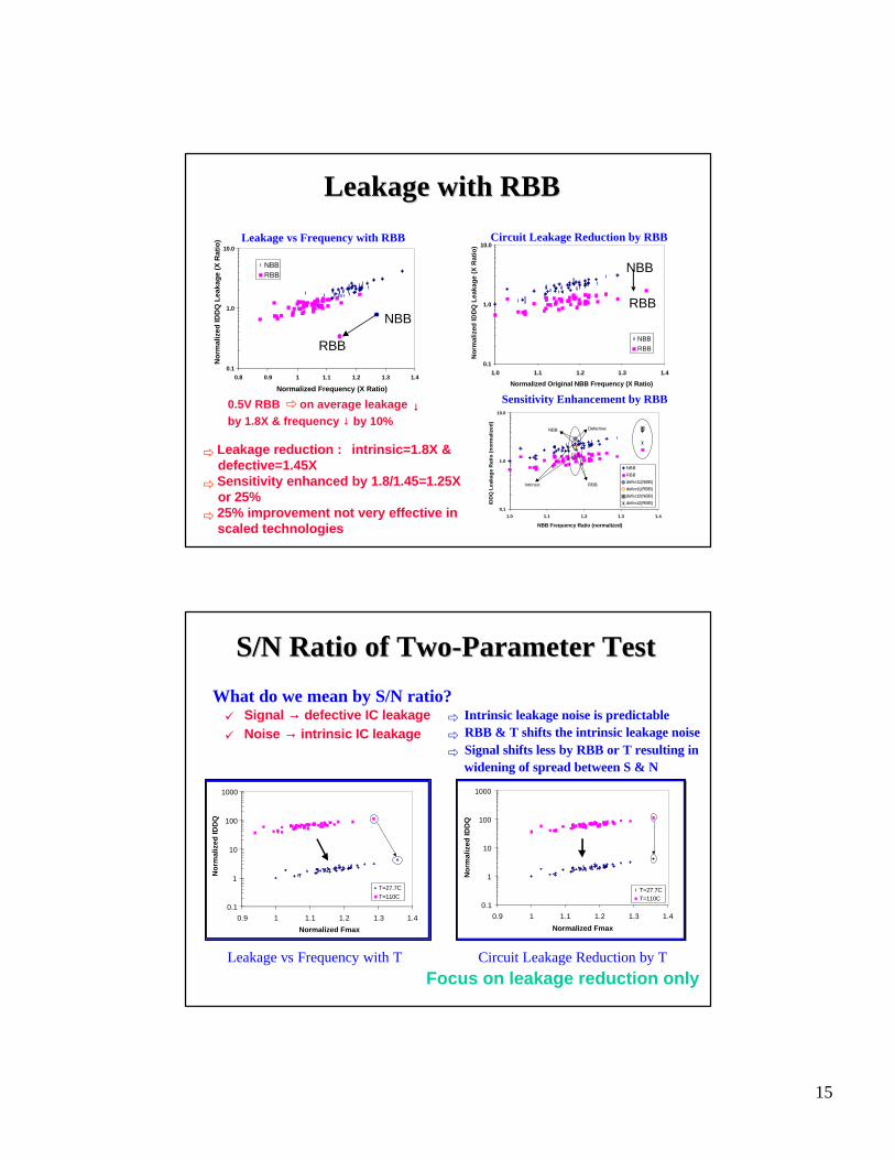
15
0.5V RBB ð on average leakage ↓↓by 1.8X & frequency ↓↓ by 10%
0.1
1.0
10.0
0.8 0.9 1 1.1 1.2 1.3 1.4
Normalized Frequency (X Ratio)
No
rmal
ized
IDD
Q L
eaka
ge
(X R
atio
)
NBBRBB
RBB
NBBFreq
lkg
NBB
RBB0.1
1.0
10.0
1.0 1.1 1.2 1.3 1.4
Normalized Original NBB Frequency (X Ratio)
No
rmal
ized
IDD
Q L
eaka
ge
(X R
atio
)
NBB
RBB
lkgNBB
RBB
NBB
RBB
Circuit Leakage Reduction by RBB
0.1
1.0
10.0
1.0 1.1 1.2 1.3 1.4
NBB Frequency Ratio (normalized)
IDD
Q L
eaka
ge
Rat
io (
no
rmal
ized
)
NBB
RBB
defect1(NBB)
defect1(RBB)
defect2(NBB)
defect2(RBB)
NBB
Intrinsic RBB
Defective
Sensitivity Enhancement by RBB
ð Leakage reduction : intrinsic=1.8X &defective=1.45X
ðSensitivity enhanced by 1.8/1.45=1.25Xor 25%
ð 25% improvement not very effective inscaled technologies
Leakage with RBBLeakage with RBB
Leakage vs Frequency with RBB
ü Signal →→ defective IC leakage
ü Noise →→ intrinsic IC leakage
What do we mean by S/N ratio?ð Intrinsic leakage noise is predictable
ð RBB & T shifts the intrinsic leakage noise
ð Signal shifts less by RBB or T resulting in widening of spread between S & N
Leakage vs Frequency with T
0.1
1
10
100
1000
0.9 1 1.1 1.2 1.3 1.4
Normalized Fmax
No
rmal
ized
IDD
Q
T=27.7C
T=110C
0.1
1
10
100
1000
0.9 1 1.1 1.2 1.3 1.4
Normalized Fmax
No
rmal
ized
IDD
Q
T=27.7CT=110C
Circuit Leakage Reduction by T
Focus on leakage reduction only
S/N Ratio of TwoS/N Ratio of Two--Parameter TestParameter Test

16
Improving Sensitivity by T
Leakage reduction: intrinsic=36X & defective=2.6XSensitivity and S/N ratio enhanced by 36/2.6=13.8X
10.0
100.0
1000.0
10000.0
0.75 1.00 1.25 1.50 1.75
Normalized Fmax Frequency (X Ratio)
No
rmal
ized
IDD
Q L
eaka
ge
(X R
atio
)
T=27.7C intrinsic room
T=110C intrinsic hot
T=27.7C Defect room
T=110C Defect hot
intrinsic
defective
improved S/N ratio
10.0
100.0
1000.0
10000.0
0.75 1.00 1.25 1.50 1.75
Normalized Fmax Frequency (X Ratio)
No
rmal
ized
IDD
Q L
eaka
ge
(X R
atio
)
T=27.7C intrinsic room
T=110C intrinsic hot
T=27.7C Defect room
T=110C Defect hot
intrinsic
defective
improved S/N ratio
0.1
1.0
10.0
100.0
1000.0
10000.0
0.75 1.00 1.25 1.50 1.75
Normalized Frequency (X Ratio)
No
rmal
ized
IDD
Q L
eaka
ge
(X R
atio
)
T=-50C
T=-25C
T=0CT=27.7C
T=50C
T=110C0.1
1.0
10.0
100.0
1000.0
10000.0
0.75 1.00 1.25 1.50 1.75
Normalized Frequency (X Ratio)
No
rmal
ized
IDD
Q L
eaka
ge
(X R
atio
)
T=-50C
T=-25C
T=0CT=27.7C
T=50C
T=110C
Adjusting Sensitivity
ð More leakage reduction is possible at a higher cost (Têê)
Sensitivity AdjustmentSensitivity Adjustment
Issues in DSM Era
• Signal integrity• DSM defects
– capacitive and inductive coupling– voltage drop - charge share– power supply noise– functional/delay faults
• New DSM fault models should support – test generation– self-test capability
• IDDQ testabilty• Diagnosis

17
High Speed Circuit Testing for Cross-Talk Defects
• Crosstalk -- One of the major noise injection mechanisms in DSM circuits
• Determine nodes that are susceptible to these faults in high-speed circuits.– Helps to generate the test pattern. – Provide guidelines to design noise tolerant circuits
Noise Sources in DSM Circuits
• Cross-talk coupling
• Power supply noise
• Charge redistribution

18
Why Noise Modeling?
• To determine the circuit immunity to noise. – Helps in designing noise tolerant circuit.
– Reduces the number of nodes to be tested.
Static Noise Margin
VDD
VOH
VIH
VIL
VOL
0 VOL VIL VIH VOH VDD
NML = |VIL - VOL|
NMH = |VOH - VIH|

19
Requirement of New Technique
New technique for testing of high-speed DSM monotonic logic circuits
Dynamic Noise ModelingStatic NM - not sufficientDynamic NM - new metric to check functional violation
Detection of functional/delay faults in a circuitEstimate propagated noise at a victim nodeComparison with dynamic noise margin
Analysis of noise immunities of high speed circuits
High Speed Circuit Testing for Cross-Talk Defects
• Crosstalk -- One of the major noise injection mechanisms in DSM circuits
• Determine nodes that are susceptible to these faults in high-speed circuits. – Helps to generate the test pattern. – Provide guidelines to design noise tolerant circuits
20
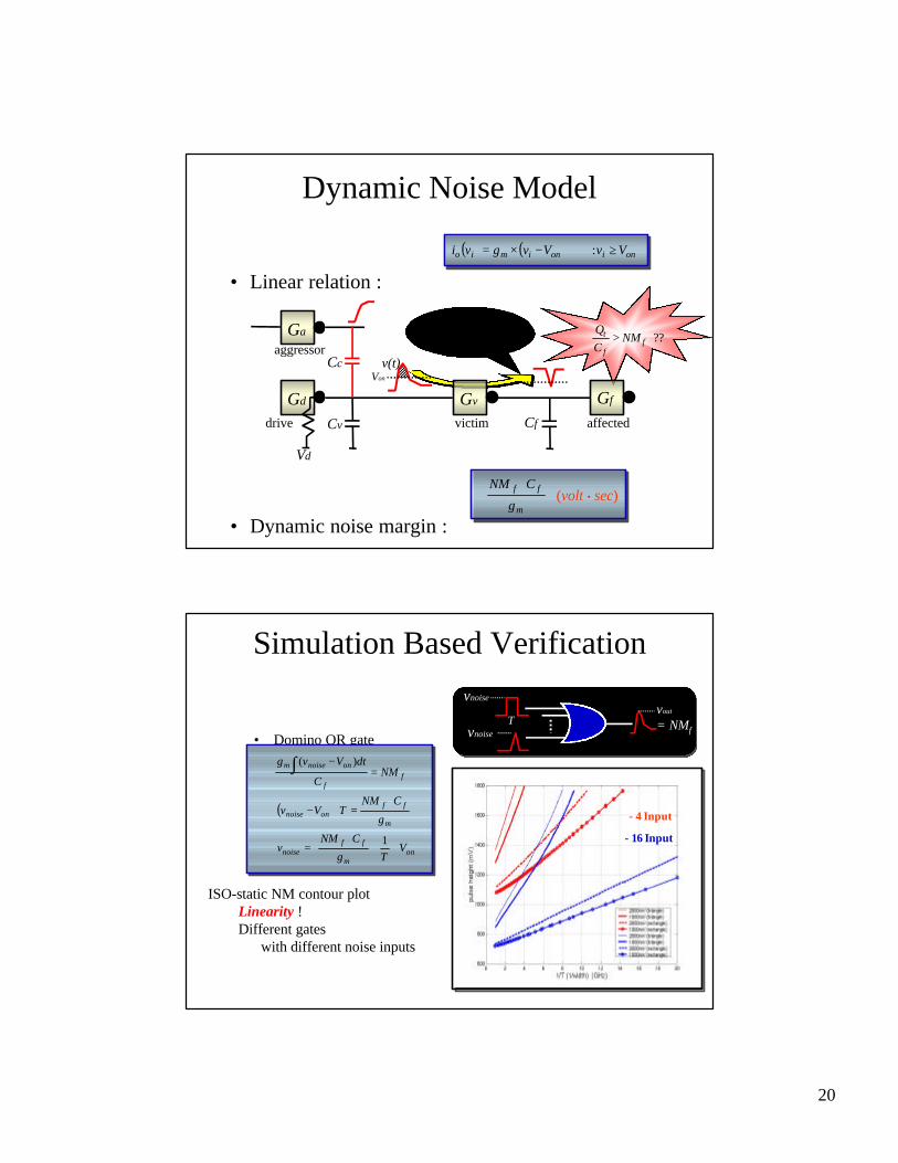
• Linear relation :
• Dynamic noise margin :
Dynamic Noise Model
aggressor
drive victim affected
Cc
Vd
Ga
Gd GfGv
Cv
v(t)Von
??ff
t NMC
Q>
Cf
( )( )∫ −⋅= dtVtvgQ onmt
( ) ( ) onionimio VvVvgvi ≥−×= :
m
ff
g
CNM ⋅(volt • sec)
Simulation Based Verification
• Domino OR gate
• For rectangular noise input
–
- 4 Input
- 16 Input
( )
onm
ffnoise
m
ffonnoise
ff
onnoisem
VTg
CNMv
g
CNMTVv
NMC
dtVvg
+⋅
⋅=⇒
⋅=⋅−⇒
=−∫
1
)(
ISO-static NM contour plotLinearity !Different gates
with different noise inputs
vnoise
vout
= NMfvnoise
vnoise
T

21
LAYOUTGATE Library CIRCUIT
CIRCUIT Levelization / R,L, & C Extraction
Static Timing Analysis
DNM calculation
Coupled noise : Vnoise(t)
Propagated noise
Propagated Noise > DNM ?Propagated Noise > DNM ?
Algorithm:
Testing for Functional FaultsTesting for Functional Faults
• Propagated Noise vs. DNM– 3 possible fault
sites
Noise Peak vs. DC NM12 possible fault sites
DNM Based VerificationCan help in reducing the cost for testing.
A 4 bit full adder circuit is verified
Results are also verified with HSPICE simulation
Testing for Functional FaultsTesting for Functional Faults

22
v(t)
Vin(t)
Coupled Noise Voltage
Victim Gate Input TransitionVd
aggressor
drive victim
Cc
Ga
Gd Gv
Cv
v(t)Von
Vin(t)
Vout(t)
t + del(Gv) + Delta
del(Gv) Gate Delay
Delta Delay induced due to coupling
Cc can be qualitative measure for delay fault
New layout architecture can help in reducing delay fault probability through Cc minimization
Delay FaultsDelay Faults
Conclusions
• Two-Parameter test with speed-adjusted leakage limit has a better S/N ratio
• It discriminates high speed leaky ICs from defective ones
• Reverse Body Bias (RBB) enhances the test sensitivity (S/N ratio) modestly
• Temperature improves the sensitivity by more than an order of magnitude (14X)
23
Conclusions
• Cross-talks faults are becoming increasing important for high-speed DSM circuits
• There is a need for good test and verification methodology for cross-talk defects

![Deep Sub-Micron Interconnects and Expectation to …...2001/01/01 · The superconnect may use around 10 micron level design rules [4]. Sometimes LSI's in the superconnect are connected](https://img.pdfslide.net/doc/110x75/60b8d3c79c65dc4b371880b3/deep-sub-micron-interconnects-and-expectation-to-20010101-the-superconnect.jpg)


![Deep Packet Inspection as a Service · Leakage Prevention Leakage Check Point DLP [11] System activity Network Analytic Protocol IDs Qosmos [13] Traffic Shaper Applications Blue](https://img.pdfslide.net/doc/110x75/606c3dc2d669f9781e40eb07/deep-packet-inspection-as-a-service-leakage-prevention-leakage-check-point-dlp-11.jpg)