Embed Size (px)
Citation preview

Defect Engineering in Semiconductors
Sili T h l bl f l l l i i• Silicon Technology: problems of ultra large-scale integration• Gettering in silicon• Defect engineering in HgCdTe• Near-surface defects in GaAs after diamond saw-cutting of wafers • The EL2-defect in GaAs
1
Defect Engineering in Semiconductors
• Silicon is most important semiconductor• degree of integration doubles after 2 years • Si not best suited for all tasks (e.g. ultra-fast applications)• but „defect engineering“ is best known for this material • MOS structures in 45 nm in current CPUs• Gate oxide: about 5 nm = 10 atoms!
Gate-Metall
n-Si n-Si
2Cross section through 0.2 µm MOSFET
Moore’s Law
source: Wikipedia
3

Example: FET-technologyCrystal growth, wafer cutting, polishing
Oxid-Schicht• photolithography 1: gate deposition
• n-conducting region by ion implantationn conducting region by ion implantation• photolithography 2: drain/source-isolation by
ion implantation• photolithography 3: deposition of Ohmic• photolithography 3: deposition of Ohmic
contacts
• several isolation layers and conducting wires
• isolation of chip‘s
• mounting in „chip carriers“ and contacts
k i• packaging
4SAINT-technology (self-aligned implantation technology)
Increasing integration
• chips have larger area (1-2 cm2); smaller structure (up to 1010 devices on a chip)• critical: metallic impurities (Verunreinigungen), e.g. Fe, Ni and Cu• < 1012 atoms/cm3 already problematic (every 10-10 atoms in Si!!)• < 1012 atoms/cm3 already problematic (every 10 10 atoms in Si!!)• they may form precipitates (Ausscheidungen); are nuclei for larger defects
• may act as electrically active deep defects (Cu in Si is donor, in GaAs acceptor)• very important for “Cu technology”, Cu is used as conductor in Si chips (better
electrical and heat conductivity – see below)• Cu must be completely embedded (e.g. by TiN – important demands: high thermal
stability, small distortions, excellent etch-stop-properties, high resistance)• irradiation defects become more important: α-radiator in packaging material as natural
isotope may shorten lifetime of component drastically
5
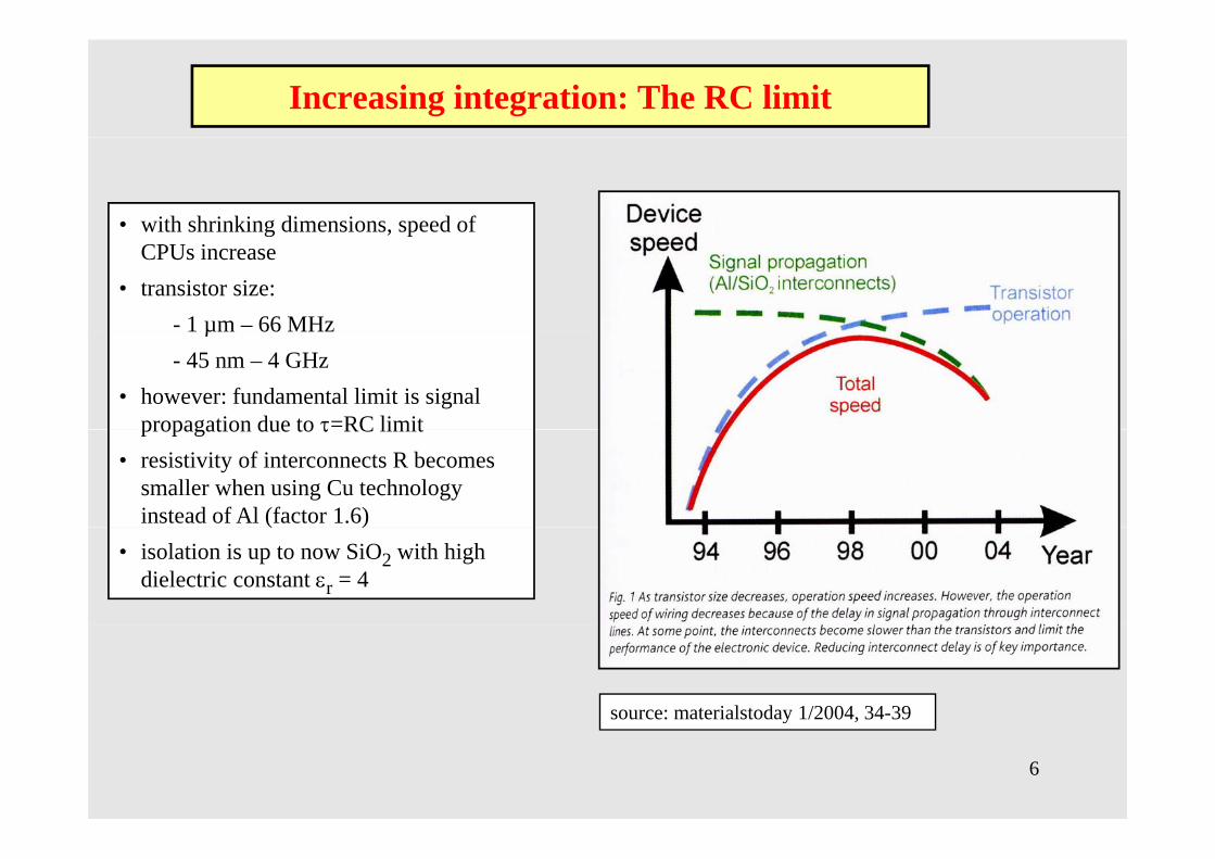
Increasing integration: The RC limit
• with shrinking dimensions, speed of g , pCPUs increase
• transistor size: - 1 µm – 66 MHz µ- 45 nm – 4 GHz
• however: fundamental limit is signal propagation due to τ=RC limitpropagation due to τ RC limit
• resistivity of interconnects R becomes smaller when using Cu technology instead of Al (factor 1.6)( )
• isolation is up to now SiO2 with high dielectric constant εr = 4
source: materialstoday 1/2004, 34-39
6
y ,
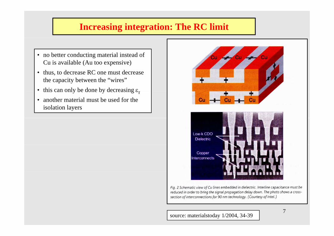
Increasing integration: The RC limit
• no better conducting material instead of Cu is available (Au too expensive)Cu is available (Au too expensive)
• thus, to decrease RC one must decrease the capacity between the “wires”
• this can only be done by decreasing εthis can only be done by decreasing εr• another material must be used for the
isolation layers
7source: materialstoday 1/2004, 34-39
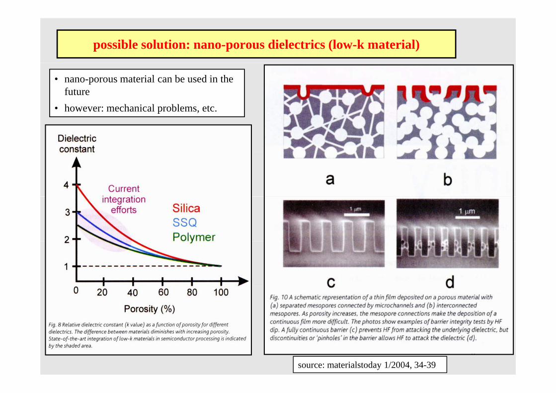
possible solution: nano-porous dielectrics (low-k material)
• nano-porous material can be used in the future
• however: mechanical problems etc• however: mechanical problems, etc.
8source: materialstoday 1/2004, 34-39
Etching / polishing of Si-Wafers
• Si is rather hard and chemically very active; natural 2 nm SiO layer• Si is rather hard and chemically very active; natural 2 nm SiO2-layer • three-stage chemo-mechanical process (patent of 1963):
1. silica-grinding (schleifen) paste in a colloid (50°C, 20 µm at a removal of 1 µ/min)absolute scratch free smooth surface then 2 machine:absolute scratch-free smooth surface, then 2. machine:
2. first step is repeated (pH-neutral, soft grinding paste)removal of only 1-2 µm Si
3 in same machine: without mechanical pressure (only chemical action)3. in same machine: without mechanical pressure (only chemical action)• extremely clean agents required for < 109 impurities/cm3
• physical cleaning of surface in UHV by heating of sample also possible (not for wafer technology but in research)technology, but in research)
• Si still contains too high density of impurities -> gettering (gettern) of diffusing impurities necessary
9
Defect engineering in Si: Gettering of impurities
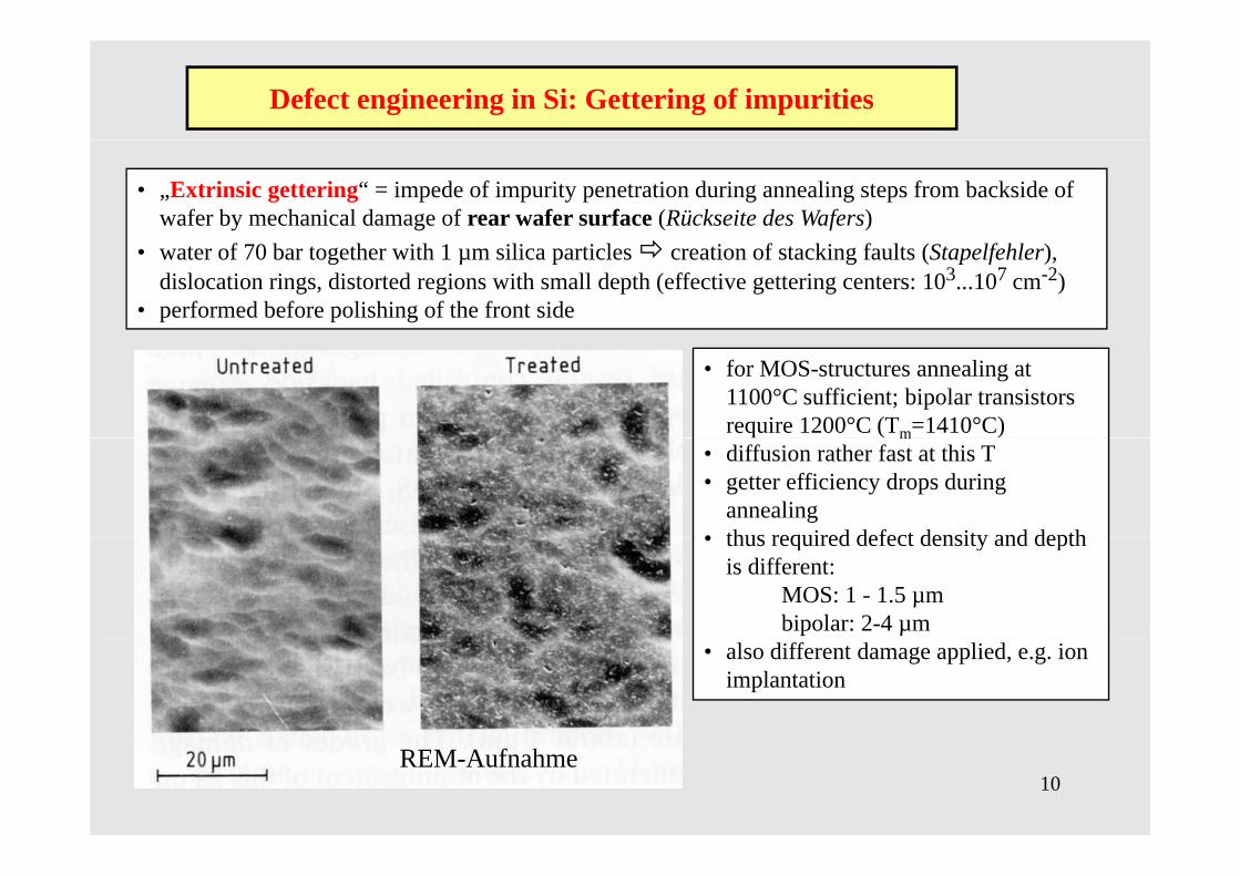
• „Extrinsic gettering“ = impede of impurity penetration during annealing steps from backside of wafer by mechanical damage of rear wafer surface (Rückseite des Wafers)
• water of 70 bar together with 1 µm silica particles creation of stacking faults (Stapelfehler), dislocation rings, distorted regions with small depth (effective gettering centers: 103...107 cm-2)
• performed before polishing of the front side
• for MOS-structures annealing at 1100°C sufficient; bipolar transistors require 1200°C (Tm=1410°C)m
• diffusion rather fast at this T• getter efficiency drops during
annealing• thus required defect density and depth• thus required defect density and depth
is different:MOS: 1 - 1.5 µmbipolar: 2-4 µm
• also different damage applied, e.g. ion implantation
10REM-Aufnahme

Extrinsic Gettering in Si
• defects also by grinding (schleifen): procedure suitable for bipolar and MOS-structures• „enhanced gettering“: additional layer is deposited at the rear surface of wafer (at 600-650°C)
without further mechanical treatmentwithout further mechanical treatment• is rather expensive, but shows best gettering effect
ll hi h d f t d itsmaller higher defect density
11
Intrinsic gettering in Si
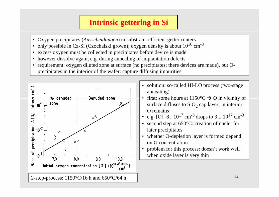
• Oxygen precipitates (Ausscheidungen) in substrate: efficient getter centers• only possible in Cz-Si (Czochalski grown); oxygen density is about 1018 cm-3
• excess oxygen must be collected in precipitates before device is madeexcess oxygen must be collected in precipitates before device is made• however dissolve again, e.g. during annealing of implantation defects• requirement: oxygen diluted zone at surface (no precipitates; there devices are made), but O-
precipitates in the interior of the wafer: capture diffusing impurities
• solution: so-called HI-LO process (two-stage annealing)
• first: some hours at 1150°C O in vicinity of• first: some hours at 1150 C O in vicinity of surface diffuses to SiO2 cap layer; in interior: O remains
• e.g. [O]=8× 1017 cm-3 drops to 3 × 1017 cm-3
• second step at 650°C: creation of nuclei for later precipitates
• whether O-depletion layer is formed depend on O concentrationon O concentration
• problem for this process: doesn’t work well when oxide layer is very thin
122-step-process: 1150°C/16 h and 650°C/64 h
Intrinsic gettering in Si
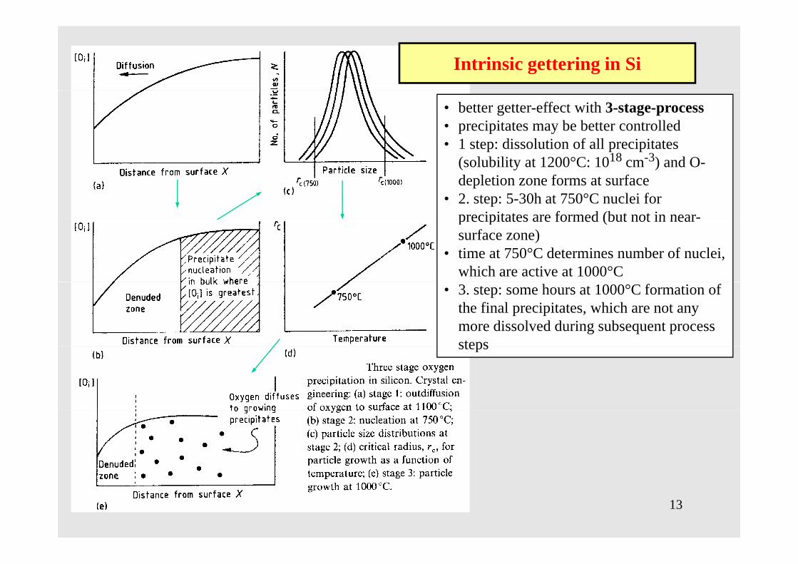
• better getter-effect with 3-stage-process• precipitates may be better controlled• 1 step: dissolution of all precipitates
18 3(solubility at 1200°C: 1018 cm-3) and O-depletion zone forms at surface
• 2. step: 5-30h at 750°C nuclei for precipitates are formed (but not in near-precipitates are formed (but not in near-surface zone)
• time at 750°C determines number of nuclei, which are active at 1000°C
• 3. step: some hours at 1000°C formation of the final precipitates, which are not any more dissolved during subsequent process stepssteps
13
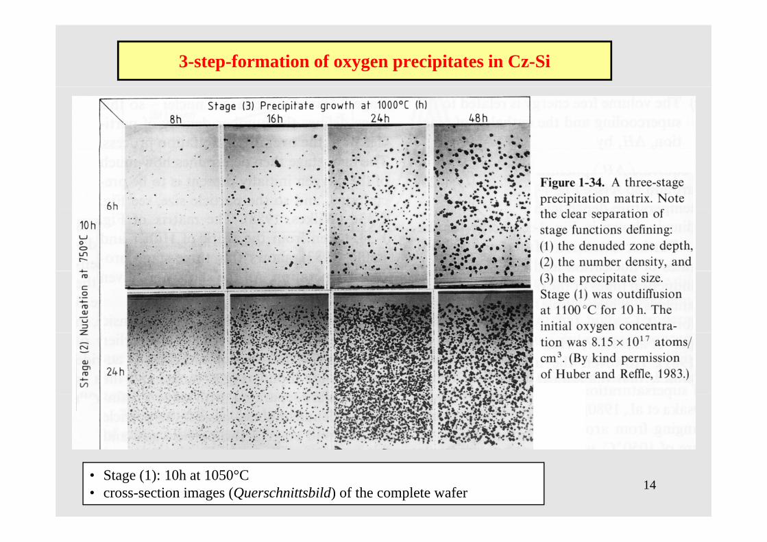
3-step-formation of oxygen precipitates in Cz-Si
14• Stage (1): 10h at 1050°C• cross-section images (Querschnittsbild) of the complete wafer
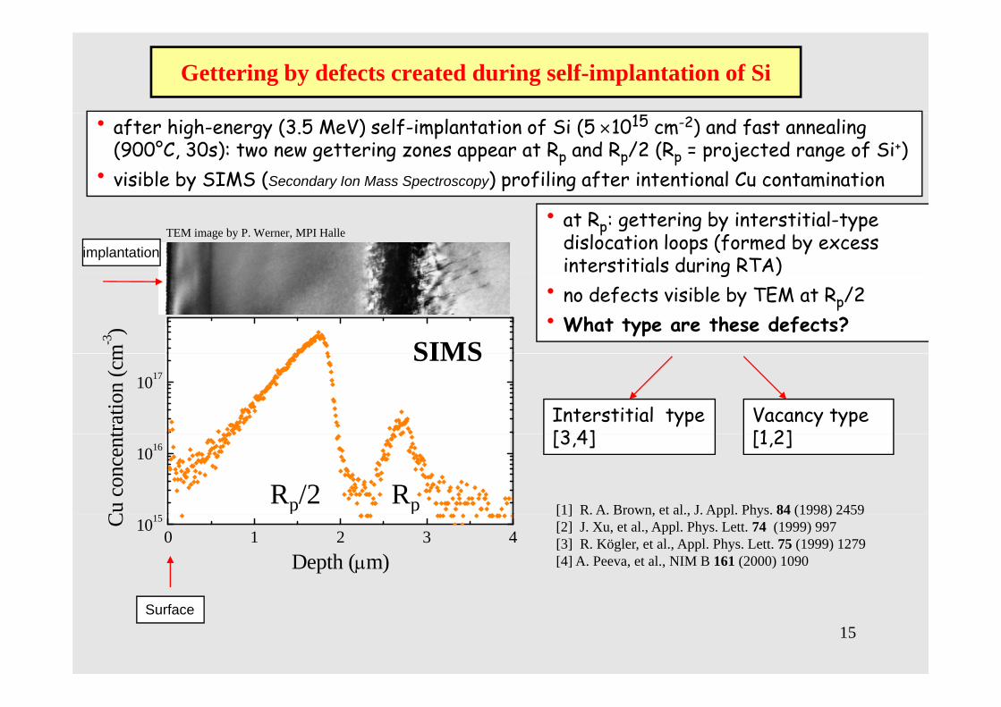
Gettering by defects created during self-implantation of Si
• after high-energy (3.5 MeV) self-implantation of Si (5 ×1015 cm-2) and fast annealing (900°C, 30s): two new gettering zones appear at Rp and Rp/2 (Rp = projected range of Si+)
• visible by SIMS (Secondary Ion Mass Spectroscopy) profiling after intentional Cu contamination
• at Rp: gettering by interstitial-type dislocation loops (formed by excess interstitials during RTA)
TEM image by P. Werner, MPI Halle
implantationg )
• no defects visible by TEM at Rp/2• What type are these defects?
m-3)
SIMS1017
tratio
n (c
m SIMS
Interstitial type [3 4]
Vacancy type [1 2]
1016
Cu c
once
nt
RpRp/2
[3,4] [1,2]
[1] R. A. Brown, et al., J. Appl. Phys. 84 (1998) 2459
0 1 2 3 41015C
Depth (μm)
[1] R. A. Brown, et al., J. Appl. Phys. 84 (1998) 2459[2] J. Xu, et al., Appl. Phys. Lett. 74 (1999) 997[3] R. Kögler, et al., Appl. Phys. Lett. 75 (1999) 1279[4] A. Peeva, et al., NIM B 161 (2000) 1090
15Surface
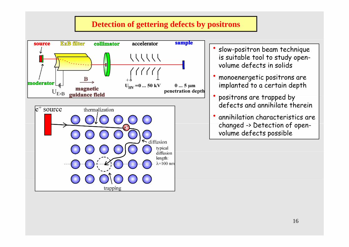
Detection of gettering defects by positrons
• slow-positron beam technique is suitable tool to study open-volume defects in solidsvolume defects in solids
• monoenergetic positrons are implanted to a certain depth
• it t d b • positrons are trapped by defects and annihilate therein
• annihilation characteristics are h d D t ti f changed -> Detection of open-
volume defects possible
16
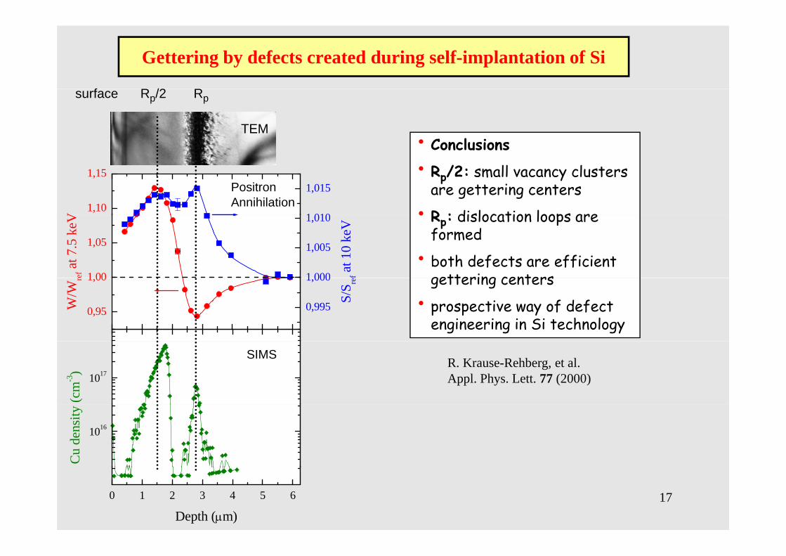
Gettering by defects created during self-implantation of Si
f RR /2
TEM
surface RpRp/2
• Conclusions
1,10
1,15
V 1 010
1,015PositronAnnihilation
• Rp/2: small vacancy clusters are gettering centers
• R : dislocation loops are
1 00
1,05
ref a
t 7.5
keV
1 000
1,005
1,010
f at 1
0 ke
V • Rp: dislocation loops are formed
• both defects are efficient gettering centers
0,95
1,00
W/W
r
0,995
1,000
S/S re gettering centers
• prospective way of defect engineering in Si technology
1017
SIMS
(cm
-3) R. Krause-Rehberg, et al.
Appl. Phys. Lett. 77 (2000)
1016
Cu
dens
ity
170 1 2 3 4 5 6
Depth (μm)
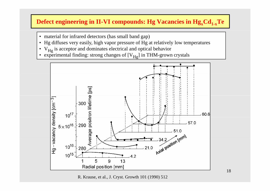
Defect engineering in II-VI compounds: Hg Vacancies in HgxCd1-xTe
• material for infrared detectors (has small band gap)• Hg diffuses very easily, high vapor pressure of Hg at relatively low temperatures• VHg is acceptor and dominates electrical and optical behaviorg• experimental finding: strong changes of [VHg] in THM-grown crystals
18R. Krause, et al., J. Cryst. Growth 101 (1990) 512

Control of VHg concentration
• Concentration of Hg vacancies can be controlled by annealing under defined vapor pressure of Hg
• all technological steps must be performed under Hg vapor pressure
19

Defects in GaAs introduced by wafer cutting
• cutting of wafer with diamond-saw (by wire and blade saws)ft tti f d t d d f t• after cutting: surface destroyed, defects
several µm deep• defect profile reaches far into the interior of
the wafer• study e.g. by positron annihilation• careful etching and polishing necessary• wafer roughness (Rauhigkeit) must be < 1
f l t 6" f50 mμ
µm for a complete 6" wafer
1.03
1.04
after sawing etching step 1 (2.5 m)μ etching step 2 (2.5 m)μ
sample 6
lk
1.01
1.02 etching step 3 (2 m)μ
S /S
bul
1.00
200 1 2 3 4 5 6 7 8 9 10
depth (μm)F. Börner et al.Appl. Surf. Sci. 149 (1999) 151-158.
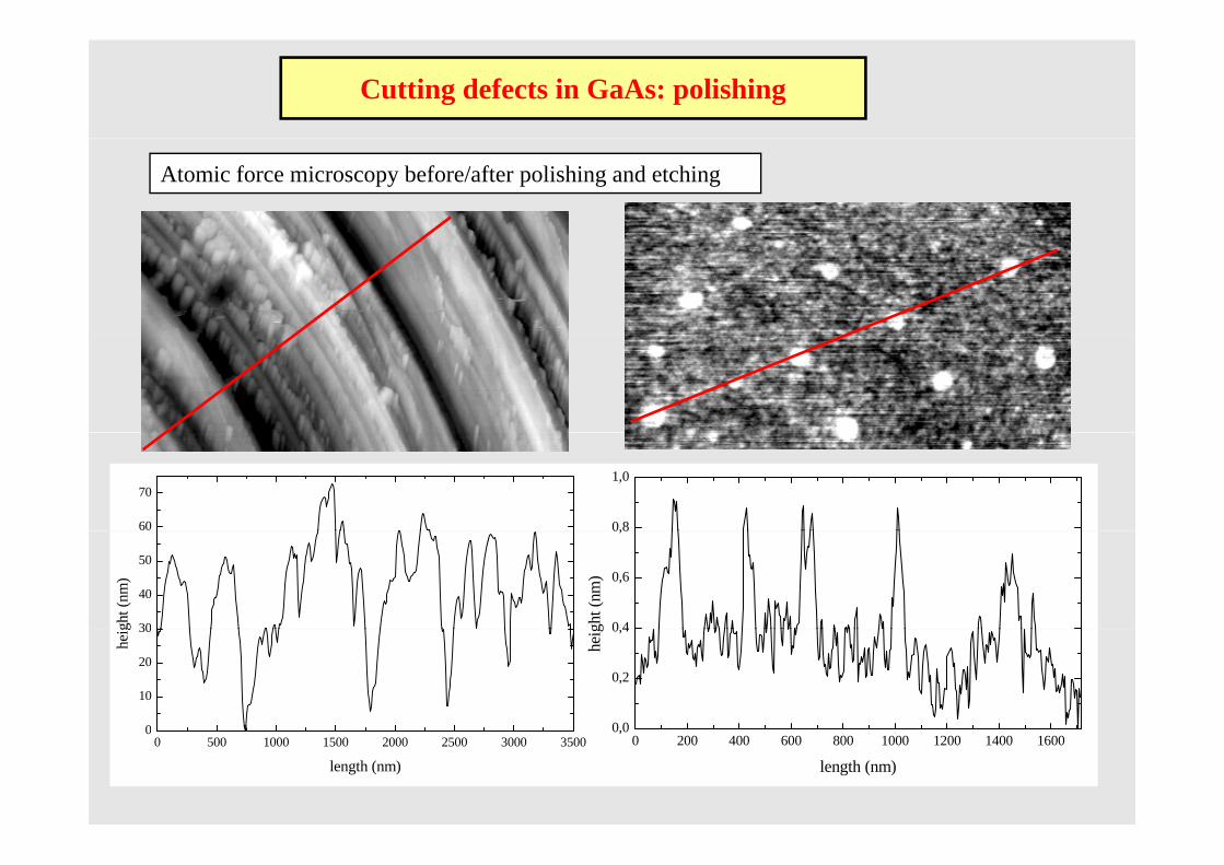
Cutting defects in GaAs: polishing
Atomic force microscopy before/after polishing and etching
0,8
1,0
60
70
0 4
0,6
0,8
ght (
nm)
30
40
50
ght (
nm)
0 0
0,2
0,4
heig
0
10
20
30
heig
21
0 200 400 600 800 1000 1200 1400 16000,0
length (nm)0 500 1000 1500 2000 2500 3000 3500
0
length (nm)
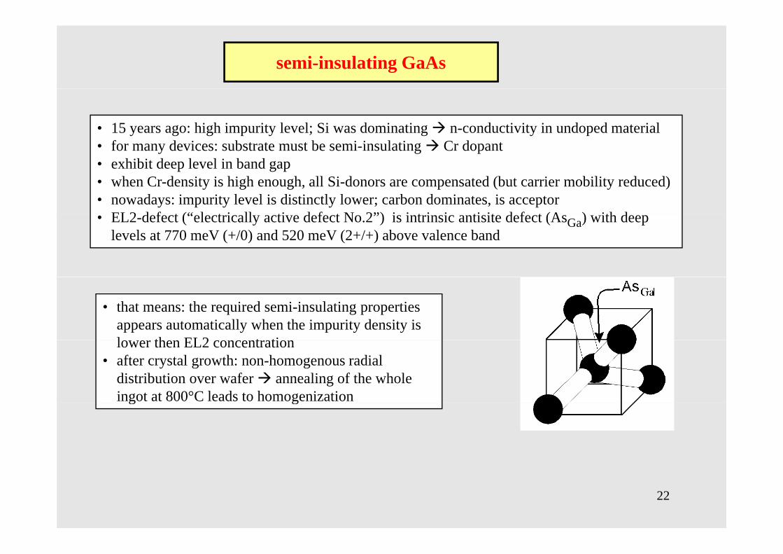
semi-insulating GaAs
• 15 years ago: high impurity level; Si was dominating n-conductivity in undoped material• for many devices: substrate must be semi-insulating Cr dopanty g p• exhibit deep level in band gap• when Cr-density is high enough, all Si-donors are compensated (but carrier mobility reduced)• nowadays: impurity level is distinctly lower; carbon dominates, is acceptor
EL2 d f t (“ l t i ll ti d f t N 2”) i i t i i ti it d f t (A ) ith d• EL2-defect (“electrically active defect No.2”) is intrinsic antisite defect (AsGa) with deep levels at 770 meV (+/0) and 520 meV (2+/+) above valence band
• that means: the required semi-insulating properties appears automatically when the impurity density is l th EL2 t tilower then EL2 concentration
• after crystal growth: non-homogenous radial distribution over wafer annealing of the whole ingot at 800°C leads to homogenization g g
22
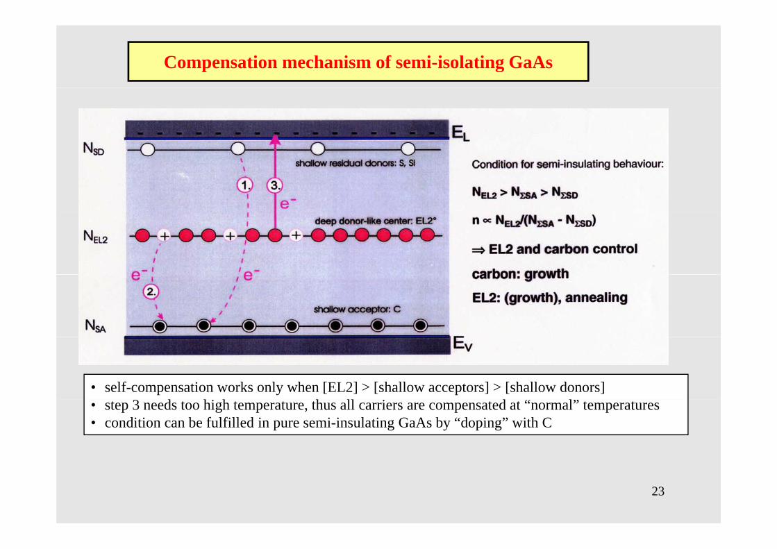
Compensation mechanism of semi-isolating GaAs
• self-compensation works only when [EL2] > [shallow acceptors] > [shallow donors]• step 3 needs too high temperature, thus all carriers are compensated at “normal” temperatures• condition can be fulfilled in pure semi-insulating GaAs by “doping” with C
23
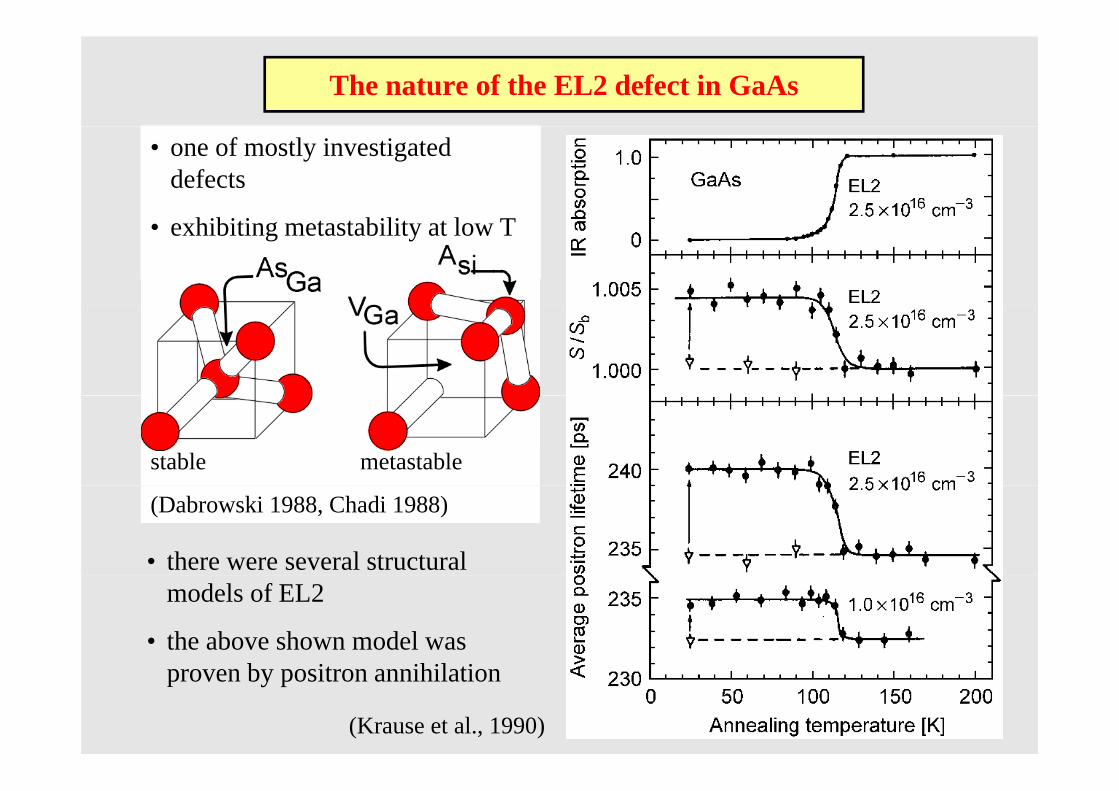
The nature of the EL2 defect in GaAs
• one of mostly investigated defects
• exhibiting metastability at low T under light illumination
stable metastable
(Dabrowski 1988, Chadi 1988)
• there were several structural models of EL2
• the above shown model was b i ihil i
24(Krause et al., 1990)
proven by positron annihilation