Embed Size (px)
Citation preview
Professor N Cheung, U.C. Berkeley
Defects TutorialEE143 F2010
1
Defects and “Damage”
• Point Defects, Point Defects clusters.Line Defects, Extended Defects
• Ion Implantation DefectsAmorphizationSecondary Defects (end-of-range loops)
• Effect of defects on
-Electrical resistivity-PN junction leakage current-Diffusion-Mechanical stress
Professor N Cheung, U.C. Berkeley
Defects TutorialEE143 F2010
2
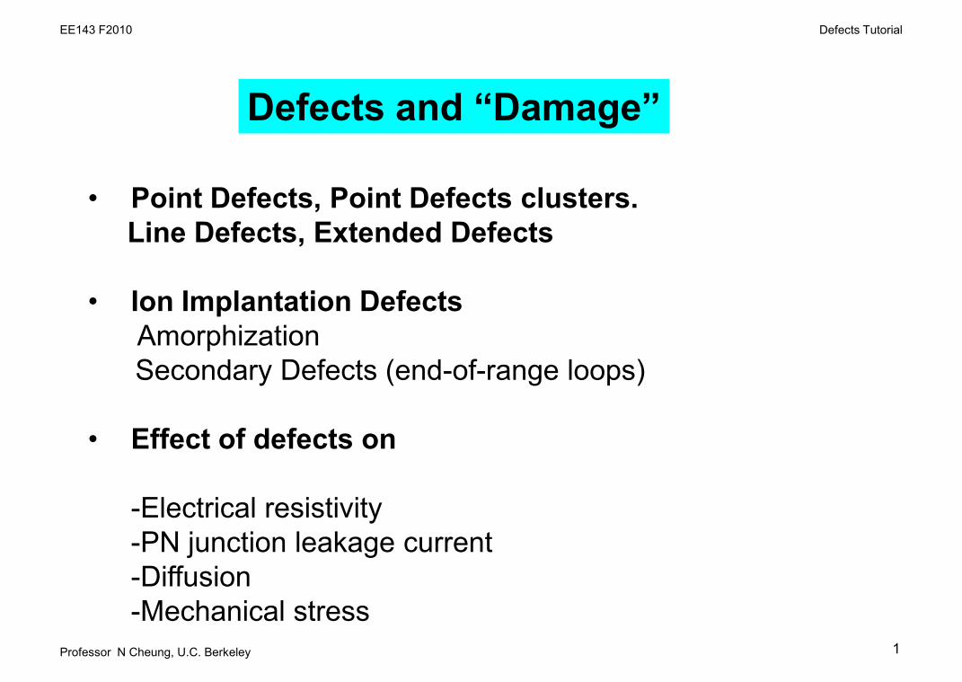
Simple Point Defects (Elemental crystal)
Professor N Cheung, U.C. Berkeley
Defects TutorialEE143 F2010
3
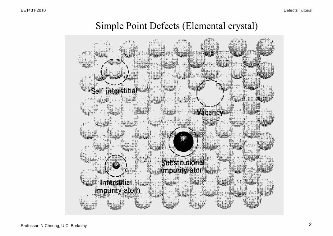
More complicated Point Defects (AB compound)
Professor N Cheung, U.C. Berkeley
Defects TutorialEE143 F2010
4
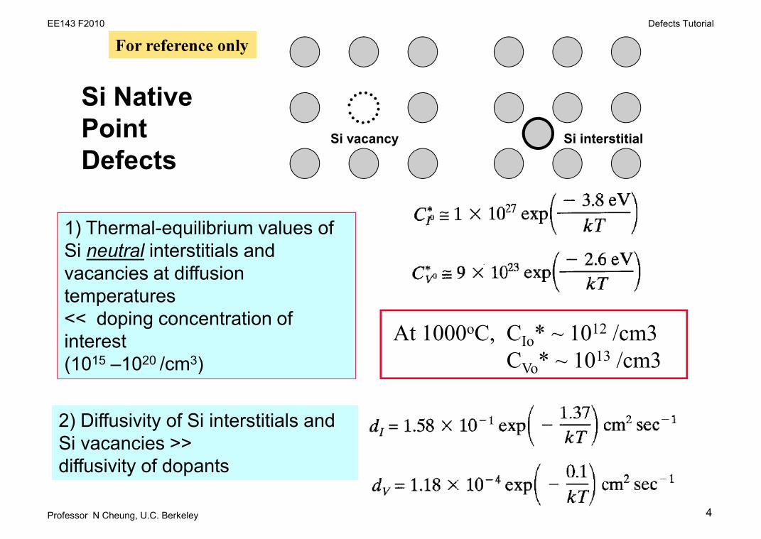
2) Diffusivity of Si interstitials andSi vacancies >>diffusivity of dopants
1) Thermal-equilibrium values ofSi neutral interstitials andvacancies at diffusiontemperatures<< doping concentration ofinterest(1015 –1020 /cm3)
Si NativePointDefects
At 1000oC, CIo* ~ 1012 /cm3CVo* ~ 1013 /cm3
For reference only
Si vacancy Si interstitial
Professor N Cheung, U.C. Berkeley
Defects TutorialEE143 F2010
5
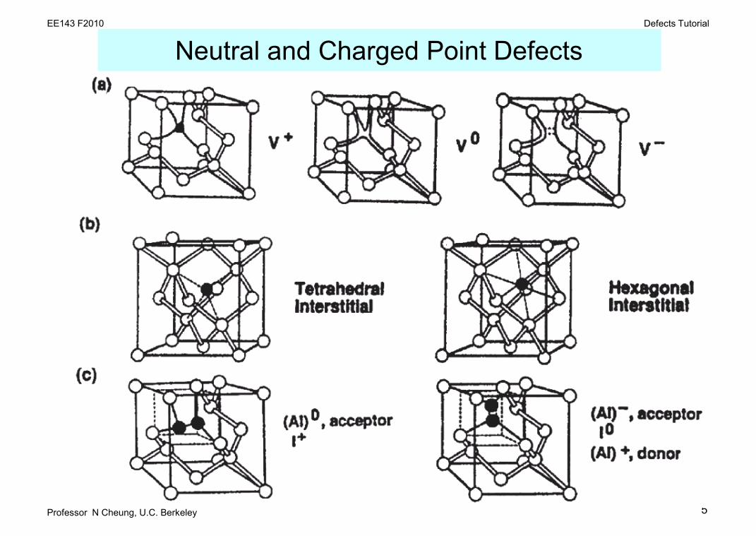
Neutral and Charged Point Defects
Professor N Cheung, U.C. Berkeley
Defects TutorialEE143 F2010
6
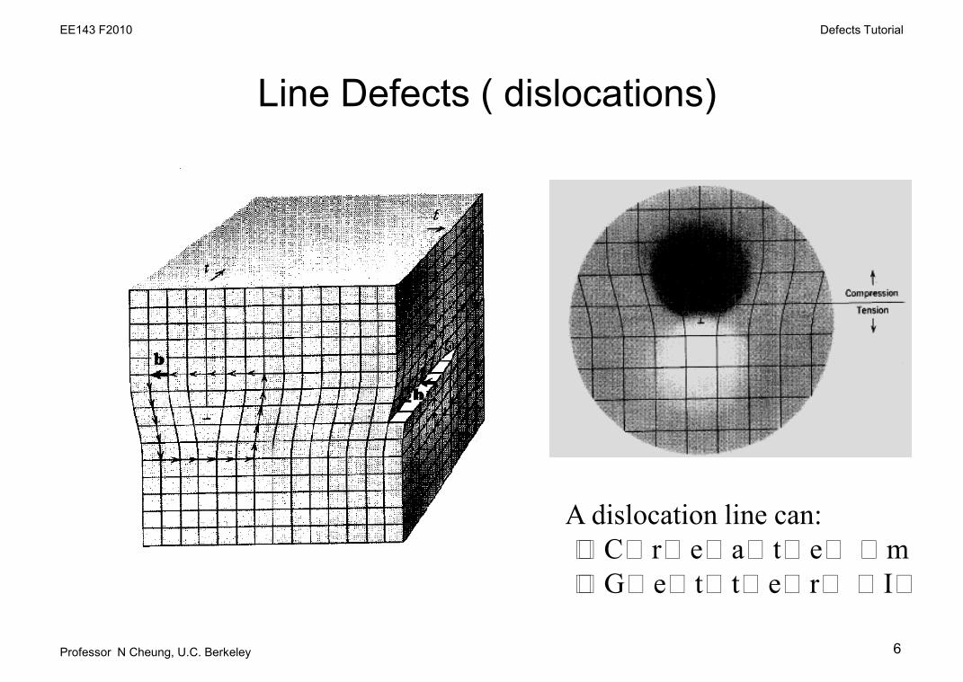
A dislocation line can:•Create mechanical stress•Getter Impurities
Line Defects ( dislocations)
Professor N Cheung, U.C. Berkeley
Defects TutorialEE143 F2010
7
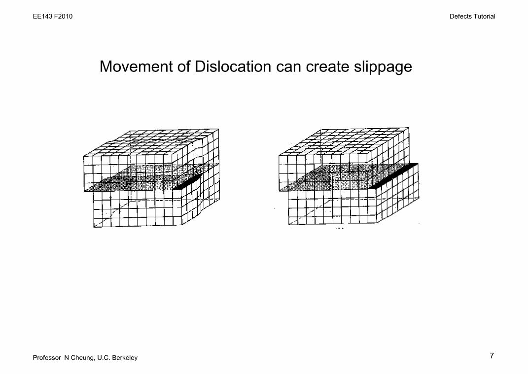
Movement of Dislocation can create slippage
Professor N Cheung, U.C. Berkeley
Defects TutorialEE143 F2010
8
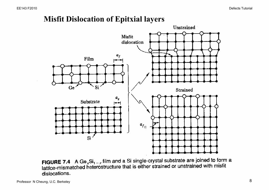
Misfit Dislocation of Epitxial layers
Professor N Cheung, U.C. Berkeley
Defects TutorialEE143 F2010
9
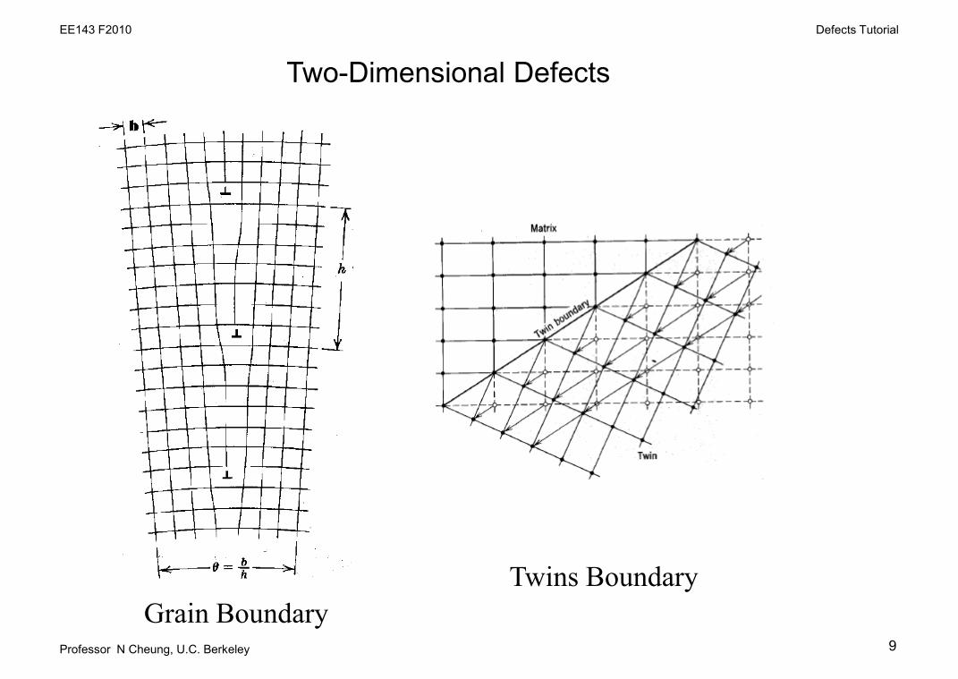
Two-Dimensional Defects
Grain BoundaryTwins Boundary
Professor N Cheung, U.C. Berkeley
Defects TutorialEE143 F2010
10
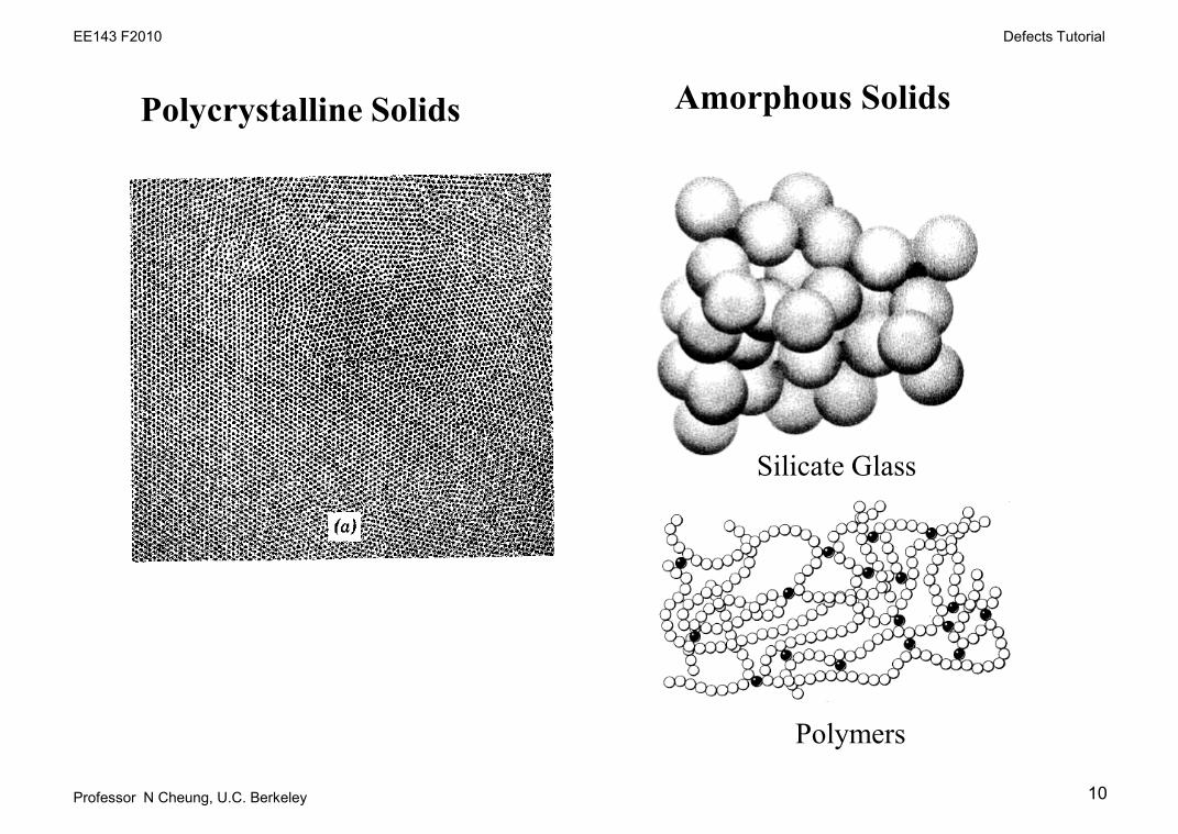
Polycrystalline Solids
Polymers
Silicate Glass
Amorphous Solids
Professor N Cheung, U.C. Berkeley
Defects TutorialEE143 F2010
11
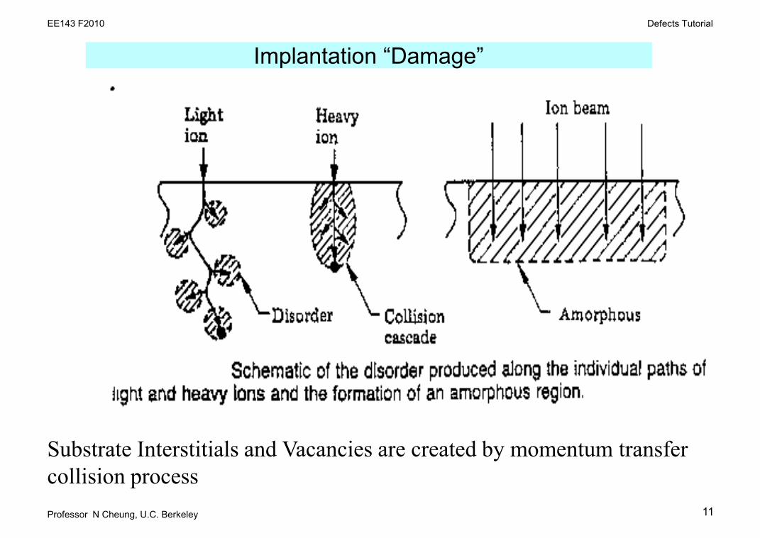
Implantation “Damage”
Substrate Interstitials and Vacancies are created by momentum transfercollision process
Professor N Cheung, U.C. Berkeley
Defects TutorialEE143 F2010
12
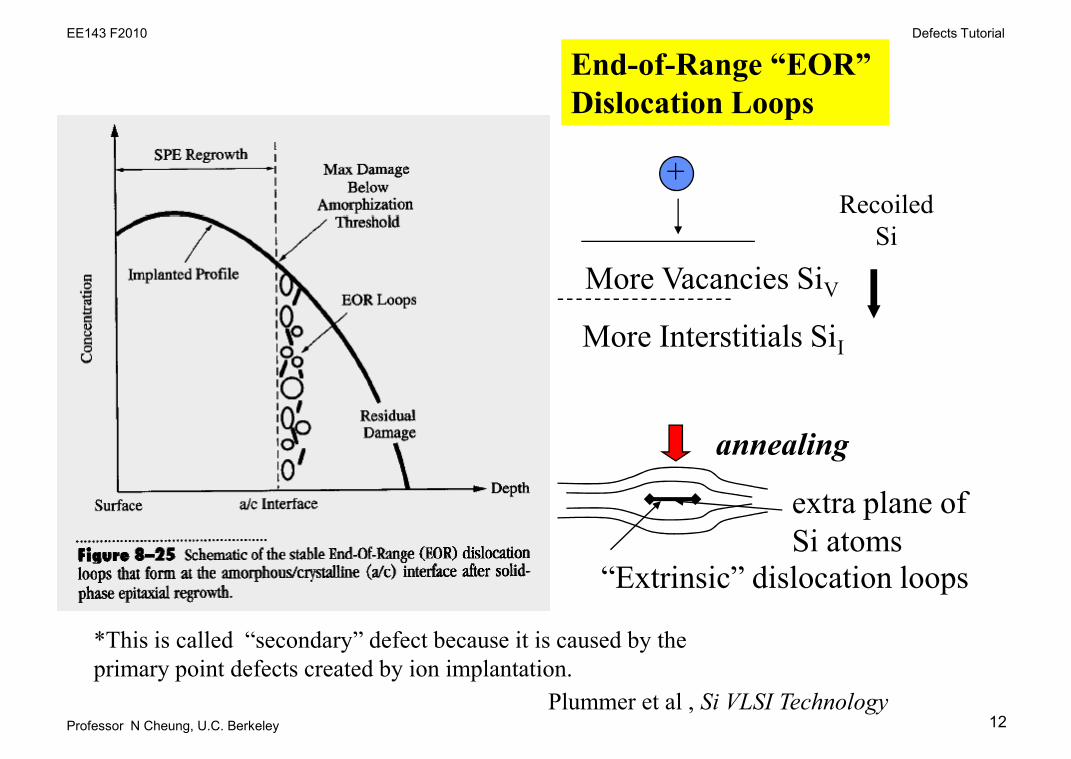
End-of-Range “EOR”Dislocation Loops
More Vacancies SiV
More Interstitials SiI
annealing
“Extrinsic” dislocation loops
extra plane ofSi atoms
Plummer et al , Si VLSI Technology
+Recoiled
Si
*This is called “secondary” defect because it is caused by theprimary point defects created by ion implantation.
Professor N Cheung, U.C. Berkeley
Defects TutorialEE143 F2010
13
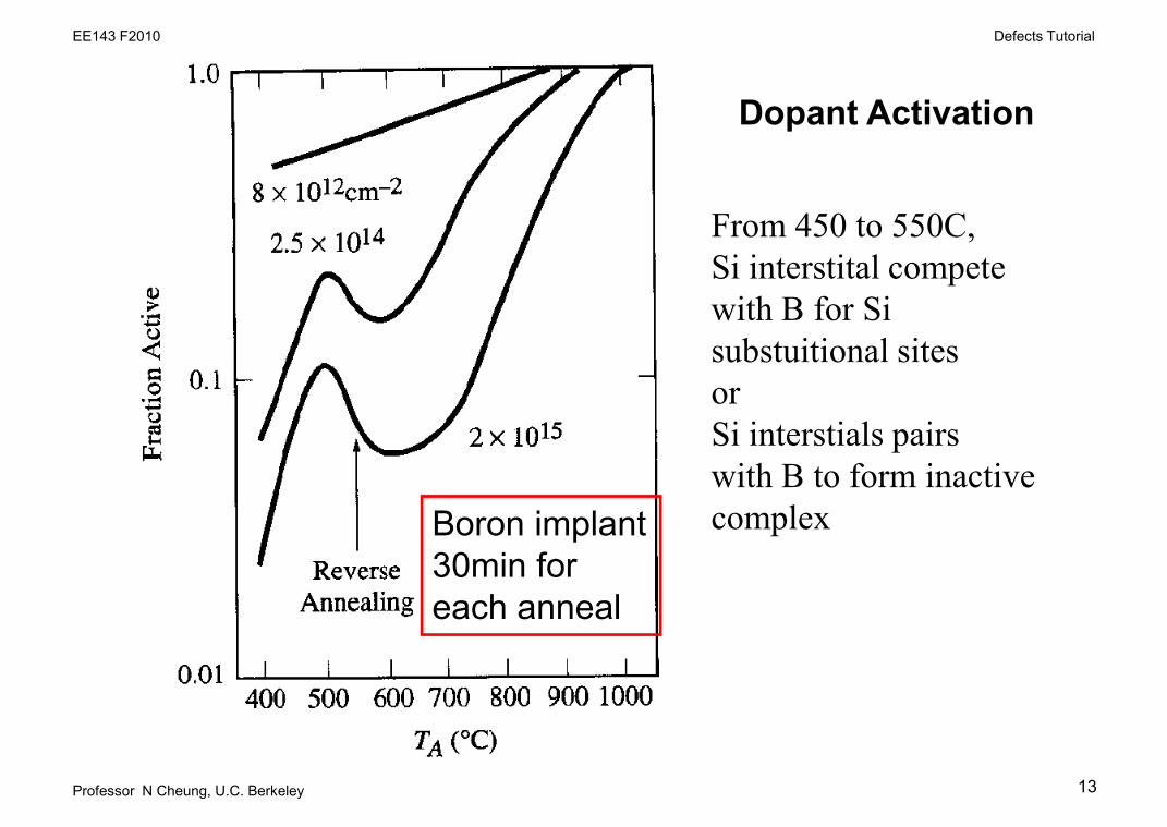
Dopant Activation
Boron implant30min foreach anneal
From 450 to 550C,Si interstital competewith B for Sisubstuitional sitesorSi interstials pairswith B to form inactivecomplex
Professor N Cheung, U.C. Berkeley
Defects TutorialEE143 F2010
14
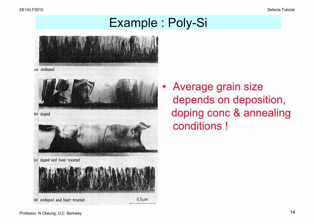
Example : Poly-Si
• Average grain sizedepends on deposition,doping conc & annealingconditions !
Professor N Cheung, U.C. Berkeley
Defects TutorialEE143 F2010
15
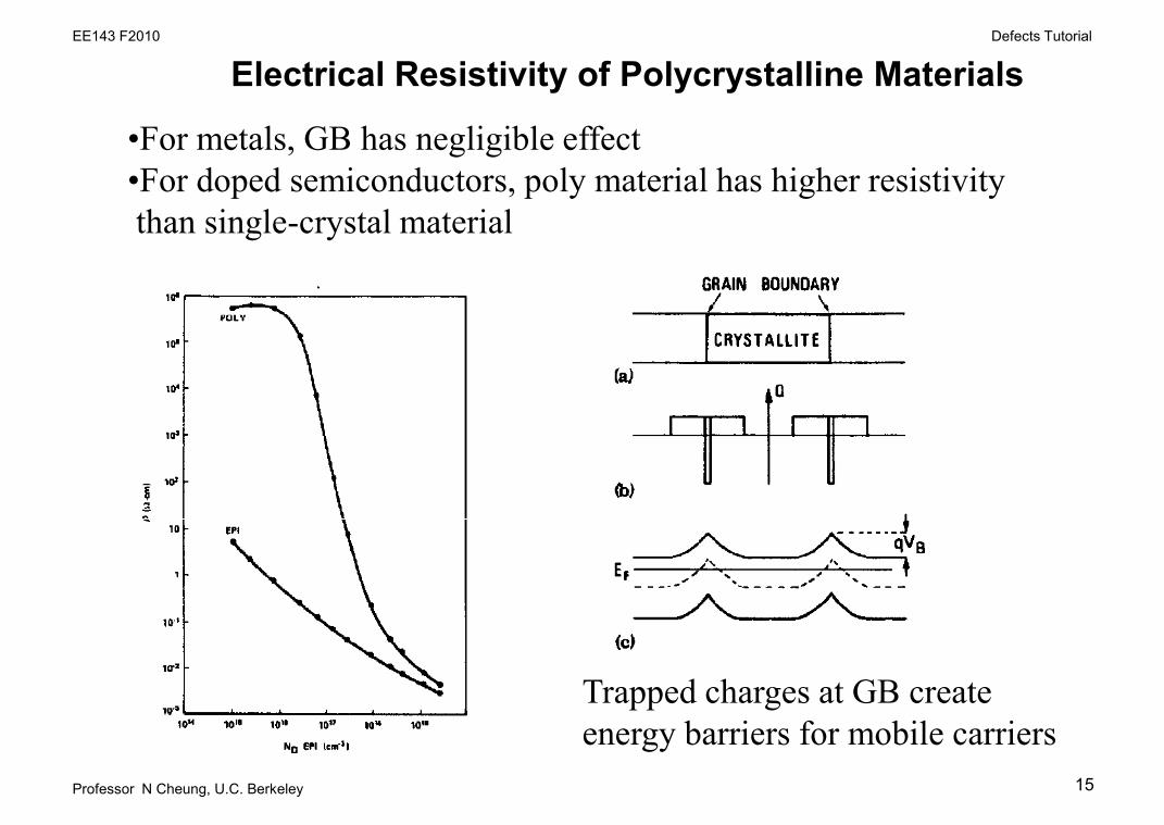
Electrical Resistivity of Polycrystalline Materials
Trapped charges at GB createenergy barriers for mobile carriers
•For metals, GB has negligible effect•For doped semiconductors, poly material has higher resistivitythan single-crystal material
Professor N Cheung, U.C. Berkeley
Defects TutorialEE143 F2010
16
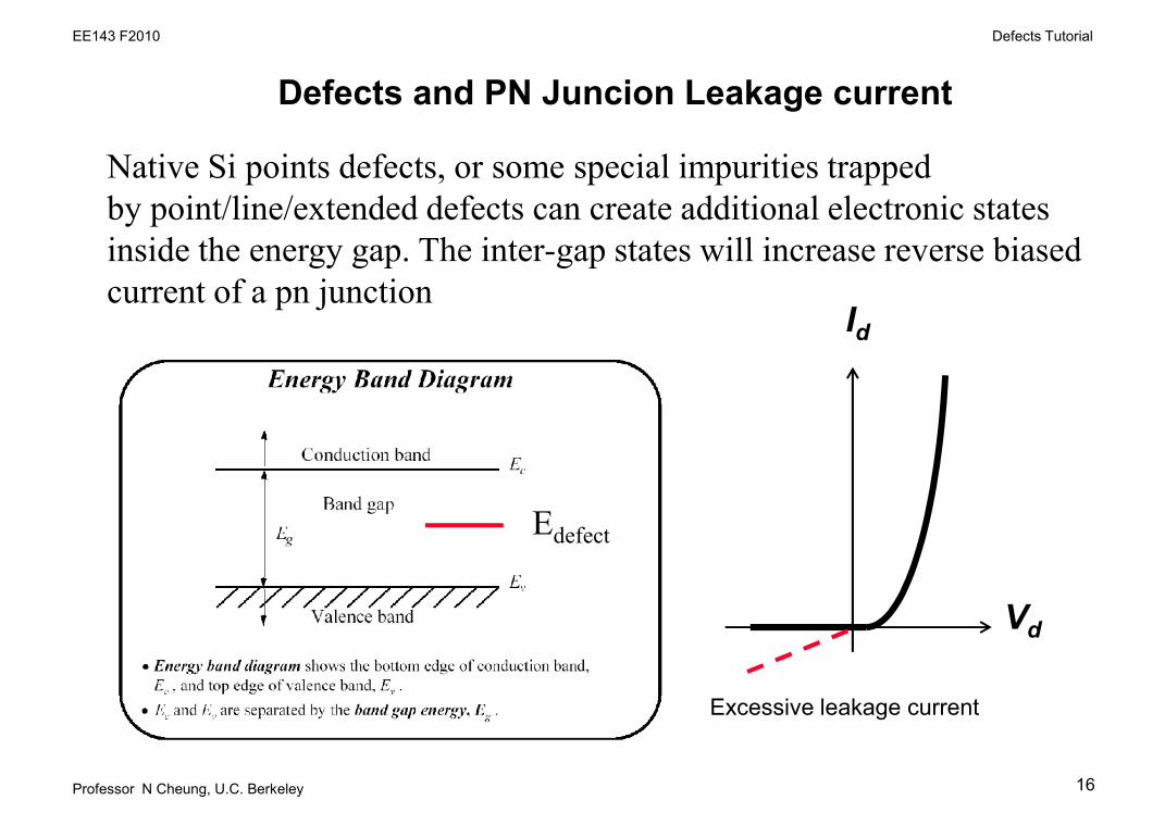
Defects and PN Juncion Leakage current
Native Si points defects, or some special impurities trappedby point/line/extended defects can create additional electronic statesinside the energy gap. The inter-gap states will increase reverse biasedcurrent of a pn junction
Id
Vd
Excessive leakage current
Edefect
Professor N Cheung, U.C. Berkeley
Defects TutorialEE143 F2010
17
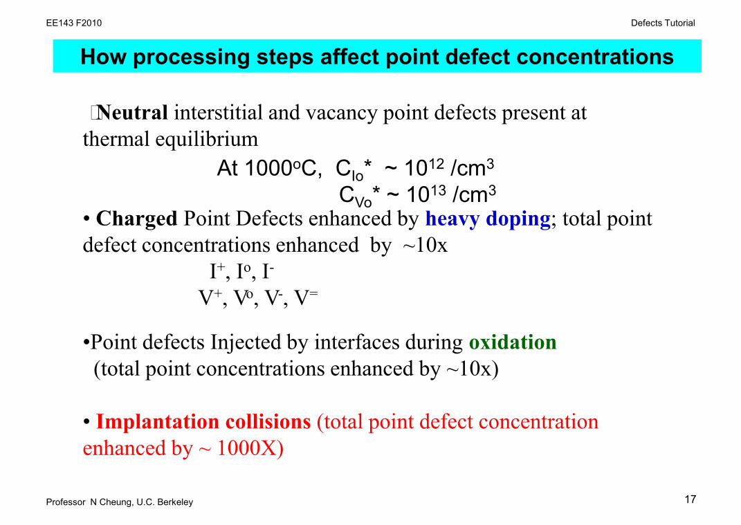
• Neutral interstitial and vacancy point defects present atthermal equilibrium
• Charged Point Defects enhanced by heavy doping; total pointdefect concentrations enhanced by ~10x
I+, Io, I-
V+, Vo, V-, V=
•Point defects Injected by interfaces during oxidation(total point concentrations enhanced by ~10x)
• Implantation collisions (total point defect concentrationenhanced by ~ 1000X)
How processing steps affect point defect concentrations
At 1000oC, CIo* ~ 1012 /cm3
CVo* ~ 1013 /cm3
Professor N Cheung, U.C. Berkeley
Defects TutorialEE143 F2010
18
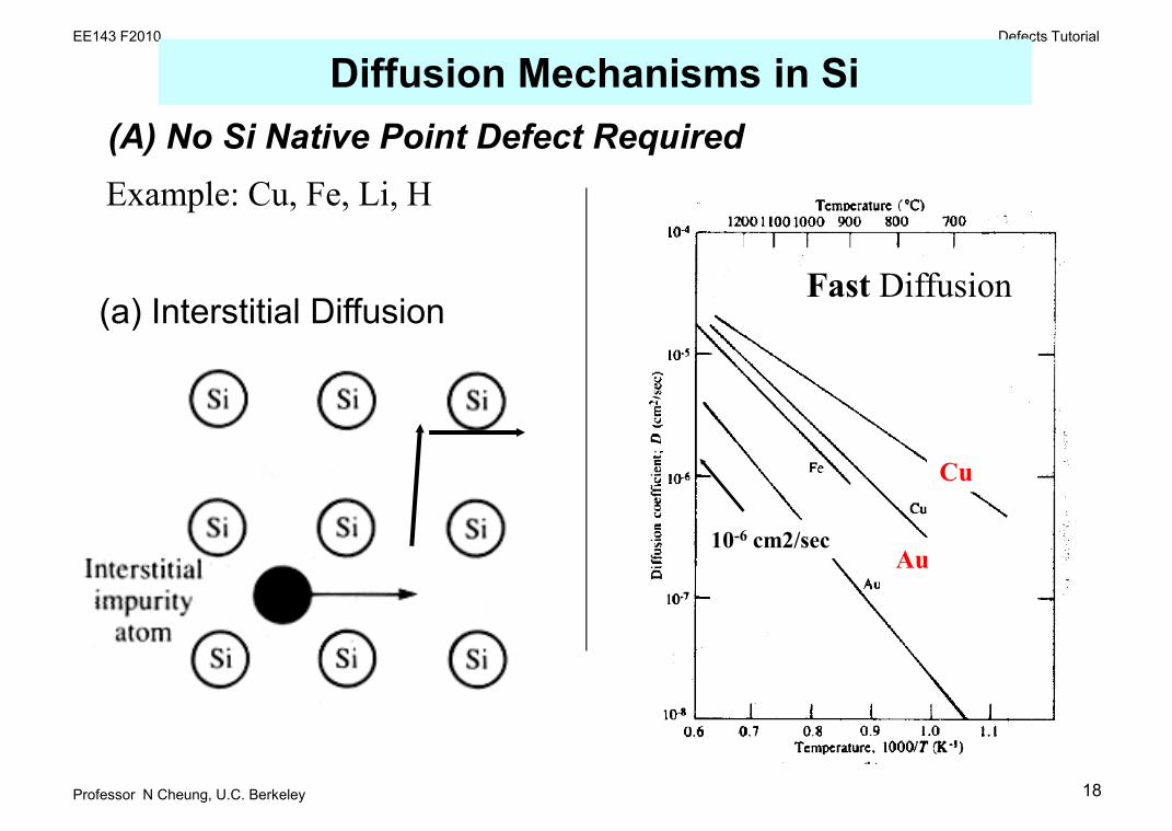
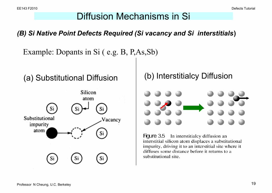
(a) Interstitial Diffusion
Diffusion Mechanisms in Si(A) No Si Native Point Defect Required
10-6 cm2/secAu
Cu
Fast Diffusion
Example: Cu, Fe, Li, H
Professor N Cheung, U.C. Berkeley
Defects TutorialEE143 F2010
19
(a) Substitutional Diffusion
Diffusion Mechanisms in Si
(B) Si Native Point Defects Required (Si vacancy and Si interstitials)
(b) Interstitialcy Diffusion
Example: Dopants in Si ( e.g. B, P,As,Sb)
Professor N Cheung, U.C. Berkeley
Defects TutorialEE143 F2010
20
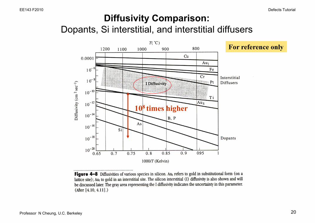
Diffusivity Comparison:Dopants, Si interstitial, and interstitial diffusers
108 times higher
For reference only
Professor N Cheung, U.C. Berkeley
Defects TutorialEE143 F2010
21
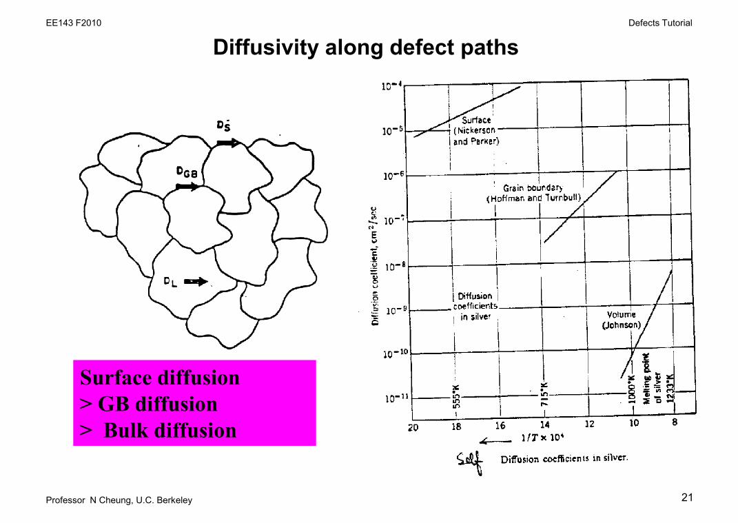
Diffusivity along defect paths
Surface diffusion> GB diffusion> Bulk diffusion
Professor N Cheung, U.C. Berkeley
Defects TutorialEE143 F2010
22
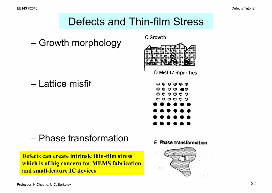
Defects and Thin-film Stress
– Growth morphology
– Lattice misfit
– Phase transformation
Defects can create intrinsic thin-film stresswhich is of big concern for MEMS fabricationand small-feature IC devices
Professor N Cheung, U.C. Berkeley
Defects TutorialEE143 F2010
23
Relevance of Defects to Microfabrication•Deposited thin films are usually polycrystalline or amorphous.One can obtain single-crystal film only with special EpitaxialGrowth conditions ( i.e., monocrystalline substrate, ultras-clean surface,and high deposition temperature)
•Monocrystalline semiconductor is needed for active regions of high-performance devices such as integrated circuits.If Polycrystalline or amorphous semiconductors is used, performance will becompromised (e.g. Poly-Si thin-film transistors, amorphous Si solar cells )
•Heavily doped Poly-Si can be used as a metallic conductor (e.g the gate materialof a MOSFET which is not part of the active device region)
•Point defect concentration and their distribution controls the diffusivity of dopants
•Defects (and the impurities they can trap) will give excess leakage currentin active device regions (e.g. pn junctions)
•Defects alter the mechanical properties ( build-in stress, fracture strength, etc)of thin films