Embed Size (px)
Citation preview

DEFENSE TECHNICAL INFORMATION CENTER
[nformiiioitforthe Deffrtse Couutauuty
Month Day Year
DTI'C® has determined on LL j that this Technical Document has the Distribution Statement checked below. The current distribution for this document can be found in the DTIC® Technical Report Database.
unl DISTRIBUTION STATEMENT A. Approved for public release; distribution is
unlimited.
] © COPYRIGHTED. U.S. Government or Federal Rights License. All other rights and uses except those permitted by copyright law are reserved by the copyright owner.
• DISTRIBUTION STATEMENT B. Distribution authorized to U.S. Government agencies only. Other requests for this document shall be referred to controlling office.
• DISTRIBUTION STATEMENT C. Distribution authorized to U.S. Government Agencies and their contractors. Other requests for this document shall be referred to controlling office.
] DISTRIBUTION STATEMENT D. Distribution authorized to the Department of Defense and U.S. DoD contractors only. Other requests shall be referred to controlling office.
• DISTRIBUTION STATEMENT E. Distribution authorized to DoD Components only. Other requests shall be referred to controlling office.
] DISTRIBUTION STATEMENT F. Further dissemination only as directed by controlling office or higher DoD authority.
Distribution Statement F is also used when a document does not contain a distribution statement and no distribution statement can be determined.
] DISTRIBUTION STATEMENT X. Distribution authorized to U.S. Government Agencies and private individuals or enterprises eligible to obtain export-controlled technical data in accordance with DoDD 5230.25.

Zap 200<Z
S-MMICs: Sub-mm-wave Transistors and Integrated Circuits
Program Final Report, submitted to
Army Research Lab BAA DAAD19-03-R-0017 Research area 2.35: RF devices—Dr. Alfred Hung
Submitted by:
Mark Rodwell, Department of Electrical and Computer Engineering, University of California, Santa Barbara, CA, 93016, rodwellfgece.ucsb.edu, 805-893-3244, -3262 fax
Table of Contents
EXECUTIVE SUMMARY 2
MOTIVATION / APPLICATION 3
TECHNOLOGY STATUS 4
TRANSISTOR SCALING LAWS 5
256 NM GENERATION 6
HBT POWER AMPLIFIER DEVELOPMENT 7
DRY-ETCHED EMITTER TECHNOLOGY: 256 NM GENERATION 9
SCALED EPITAXY 11
CONCLUSIONS 12
20081103013

Executive Summary Transistor and power amplifier IC technology was developed under UCSB for the DARPA SWIFT program. SWIFT seeks to develop sub-mm-wave transistors and ICs to support 340 GHz-band imaging and radar systems. By program end, HBT power-gain cutoff frequencies were increased to 880 GHz, simultaneous with a ~5 V breakdown voltage. HBT layer structure designs and process flows, and initial 340 GHz power amplifier designs developed at UCSB were transferred to Teledyne Scientific. Teledyne Scientific then fabricated both transistors and ICs under the financial support of a separate DARPA program; results at TSC include a 2 mW power amplifier at 340 GHz.
Device technology development at UCSB included a number of significant accomplishments supporting the future development of sub-mm-wave transistors and integrated circuits, including all-dry-etched processes for reliable formation of-128 nm feature size transistor emitters and ultra low resistivity contacts for the emitter and base contacts. These several features are critical in enabling transistor bandwidths to extend to the low THz regime.
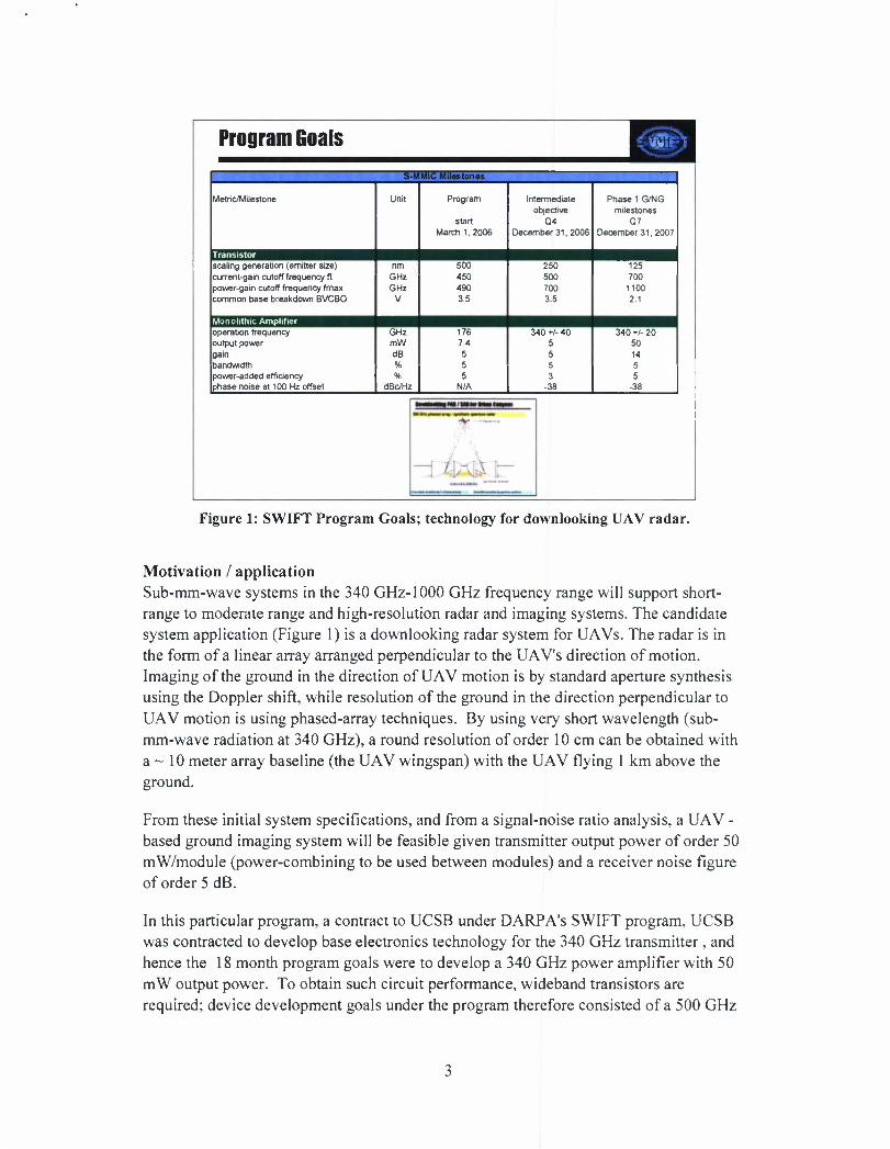
Program Goals S-MMIC Milestones
Metric/Milestone Unit Program
start March 1, 2006
Intermediate objective
Q4 December 31, 2006
Phase 1 G/NG milestones
Q7 December 31. 2007
Transistor scaling generation (emitter size) current-gain cutoff frequency ft power-gain cutoff frequency fmax common base breakdown BVCBO
nm GHz GHz
V
500 450 490 3.5
250 500 700 3.5
125 700 1100 2.1
Monolithic Amplifier operation frequency output power gain bandwidth power-added efficiency phase noise at 100 Hz offset
GHz mW dB % %
dBc/Hz
176 7.4 5 5 5
N/A
340 +/- 40 5 5 5 3
-38
340 +/- 20 50 14 5 5
-38
Figure 1: SWIFT Program Goals; technology for downlooking UAV radar.
Motivation / application Sub-mm-wave systems in the 340 GHz-1000 GHz frequency range will support short- range to moderate range and high-resolution radar and imaging systems. The candidate system application (Figure 1) is a downlooking radar system for UAVs. The radar is in the form of a linear array arranged perpendicular to the UAVs direction of motion. Imaging of the ground in the direction of UAV motion is by standard aperture synthesis using the Doppler shift, while resolution of the ground in the direction perpendicular to UAV motion is using phased-array techniques. By using very short wavelength (sub- mm-wave radiation at 340 GHz), a round resolution of order 10 cm can be obtained with a ~ 10 meter array baseline (the UAV wingspan) with the UAV flying 1 km above the ground.
From these initial system specifications, and from a signal-noise ratio analysis, a UAV - based ground imaging system will be feasible given transmitter output power of order 50 mW/module (power-combining to be used between modules) and a receiver noise figure of order 5 dB.
In this particular program, a contract to UCSB under DARPA's SWIFT program, UCSB was contracted to develop base electronics technology for the 340 GHz transmitter , and hence the 18 month program goals were to develop a 340 GHz power amplifier with 50 mW output power. To obtain such circuit performance, wideband transistors are required; device development goals under the program therefore consisted of a 500 GHz

fT , 700 GHz /max HBT at the 250 nm scaling generation, with a target date of Dec. 31,
2006, and of a 700 GHz ft , 1100 GHz /max HBT at the 125 nm scaling generation, with
a target date of Dec. 31, 2007, the phase 1 program end date.
Technology Status
Present Status of Fast lll-V Transistors
Updated Jan 2006 I I I I | I I I I | I I I I | I I I I | I
100 200 300 400
f (GHz)
1111111111111111
500 600 700 800
popular metrics:
(/, +/-V2
(V/.+V/-.)'1
much better metrics:
power amplifiers:
PAE, associated gain,
mW/^m
low noise amplifiers:
F^,,, associated gain,
digital:
fcM, hence
(C„Af//,),
Figure 2: HBT Performance at Program Start, January 2006
inPDHBTs: September 2008 popular metrics:
ftor /ir»x alone
TeledyneDBHT (/. +f*~)12
UIUC DHBT
NTT DBHT
ETHZ DHBT
UIUCSHBT
UCSB DHBT
NGSTDHBT
HRLDHBT
BM SiGe
Vitesse DHBT
f (GHz)
4fJ^ (V/r+l//-)"*
much better metrics: power amplifiers:
PAE, associated gain,
mW/fm
low noise amplifiers:
F».,> • associated gain,
digital:
fM, hence
icjunt.).

Figure 3: HBT Performance at final program review, September 2008. Note the change in ft, fmax axes.
Figure 2 and Figure 3 compare the performance of HBTs over the period January 2006 to September 2008. In this period, the HBT /max has been increased from 500 to 900 GHz.
Transistor scaling laws
HBT scaling laws Goal: double transistor bandwidth when used in any circuit
-> keep constant all resistances, voltages, currents —> reduce 2:1 all capacitances and all transport delays
rb = Tb2/2D„ + Tblv — thin base -1.414:1
TC = TJ2V — thin collector 2:1
• reduce junction areas 4:1 - reduce emitter contact resistivity 4:1
c* « Acrrc
K=PJA, 1 xA/T2 (current remains constant, as desired) chirk c c ' (emitter length Lh
P ( L, | P neetf to reduce Junction areas 4:1 A T - ~Z 7~ln 77T + IP T~ reduce widths 2:1 & reduce length 2:1 — doubles ATX
Rbb,M,+ P^ + ^
reducing widths 4:1, keep constant length-' small A T increase •/
— reduce base contact resistivity 4:1
reduce widths 2:1 & reduce length 2:1 —> constant Rbb * "* reducing widths 4:1, keep constant length —> reduced Rbt) S•/
Linewidths scale as the inverse square of bandwidth because thermal constraints dominate.
12/.. 61
Figure 4: HBT Scaling Laws
Figure 4 illustrates HBT scaling laws. For each 2:1 increase in device bandwidth the collector layer must be thinned 2:1, the lithographic dimensions reduced 4:1, the current density increased 4:1 and the resistivities of the Ohmic contacts reduced 4:1. In addition to the challenges in developing fabrication processes which permit this rapid reduction in device dimensions, the underlying challenges are in the great difficulties faced in producing very low resistivity contracts, and in the difficulties faced in managing self- heating at such high current densities. Developed from the scaling laws of Figure 4, Figure 5 shows a scaling roadmap for mixed-signal HBTs. For sub-mm-wave HBTs such as needed in the SWIFT program, the scaling roadmap is similar except that collect thicknesses -— 1.5:1 larger are employed, as this somewhat increases HBT /max, albeit at
some sacrifice in digital speed.

Multi-THz InP HBT Scaling Roadmap Es-U
emitter 512
16 256 8
128 4
64 2
32 nm width 1 O-jim2 access p
base 300 20
175 10
120 5
60 2.5
30 nm contact width, 1.25 Q- \xm2 contact p
collector 150
4,5 106 9
75 18
53 36
37.5 nm thick, 72 mA/mn2 current density
4,8 4 3,3 2,75 ~2 V. breakdown
f, 370 'max 490
power amplifiers 245 digital 2:1 divider 150
520 850 430 240
730 1300 660 330
1000 2000 1000 480
1400 GHz A 2800 GHz M 1400 GHz —W— 660 GHz
Figure 5 HBT Scaling Roadmap
256 nm generation
Figure 6: SEM Images of HBTs fabricated under SWIFT; 256 nm scaling generation.

256 nm Scaling Generation DHBTs 150 nm thick collector
40
70 nm thick collector 60 nm thick collector
40-
3C-J
Proportionally scaled device lull potential I, and f„r achieved.
Significant sacrifice in I, and fmu
arising from imbalanced scaling. collector much too thin for 256 nm generation* compromised f,andfm^ Device is for breakdown measurement.
Figure 7: RF and DC parameters of HBTs at the 256 nm generation.
During the first 9 months of effort under SWIFT, HBTs were fabricated using standard mesa processes (Figure 6). Junction dimensions were reduced, epitaxial layers were made thinner, and contact resistivities were decreased. The results (Figure 7) included devices at 150 nm collector thickness with 780 GHz fmax and devices with 60 nm
collector thickness showing 660 GHz fT .
HBT power amplifier development Subsequent to the development of the 780 GHz /max HBT at UCSB, power amplifier
design was initiated. Mask designs included (Figure 8) versions of up to 60 mW saturated output power. These designs were not successfully fabricated at UCSB. Both IC designs and HBT process flows for the 256 nm scaling generation were therefore transferred from UCSB to Teledyne Scientific and Imaging Inc. (TSC), who subsequently fabricated lower-power versions of the design (Figure 9). An output power of 2 mW was obtained in a single-HBT design.

UCSB Amplifier Designs
• 8 to 16 finger two-stage design
• 2 finger single-stage design
• Shown with large pad structures used for S-paramctcr measurements
• Two-stage design yields -60 mW
• Small signal amp gives 7.2 dB
Figure 8: Mask Layouts of 340 GHz power amplifiers designed at UCSB
324 GHz Medium Power Amplifiers in 256 nm HBT
ICs designed by Jon Hacker/ Teledyne
Teledyne 256 nm process flow-
Hacker et al, 2008 IEEE MTT-S
~2mW saturated output power 20 • • • • I ••••I• • i • I • • • • I • • • •I••••! i • • — Output Power (dBm) —• Gain (dB) ^— Drain Current (mA) J - - PAE (%)
40
-15 -10 -5 0 Input Power (dBm)
Figure 9: 2 mW 340 GHz TSC/UCSB power amplifier

Dry-Etched Emitter Technology: 256 nm generation
Process Must Change Greatly for 128 / 64 / 32 nm Nodes
control undercut —> thinner emitter thinner emitter
—> thinner base metal thinner base metal -»excess base metal resistance
Undercutting of emitter ends
{101}A planes: fast
^^ {111}A planes: slow
Figure 10: Difficulties faced in scaling HBT process flows to 128 nm & below.
128 nm Emitter Process: Dry Etched Metal & Semicon Litho pattern
metal sidewall dry etch
Si02
TiW
InGaAs n++
InPn
InGaAs p++ Base
InGaAs n++
InPn
InGaAs p++ Base
InGaAs n++
InPn
InGaAs p++ Base
InPn
InGaAs p++ Base InGaAs p++ Base
f = 560 GHz\ max
f = 560 GHz
109 10'° 10" 1012
Hz
results @ c.a. 200 nm emitter metal width
Figure 11: Dry-etched emitter process.

As shown in Figure 6, standard mesa and liftoff HBT processes can be used to build devices at 256 nm emitter feature size. At smaller sizes (Figure 10), two major difficulties arise. First, in making the emitter more narrow, emitter etch undercut must be reduced. This requires thinning the emitter, which (in a liftoff process) then requires thinning the base metal. High base metal access resistance then results from such thin metal layers, and the HBT fmax drops. A second difficulty arises from wet-etching the
emitter. While the etch facets of InP allow the lateral etch rate to be low, reducing the lateral undercut on the emitter sides, facet effects result in very rapid undercutting of the emitter ends, particularly for very narrow emitters. For these reasons, wet etched and lifted-off processes were abandoned at the 128 nm generation.
First Result @128 nm Generation
target 700 GHz fT, 1300 GHz fTOX when mature here: first working devices
Dry-etched, refractory (TiW) emitter metal Dry-etched emitter-base junction Double-sidewall process for emitter adhesion
Process accidents: poor emitter, collector contacts High f^, good p nevertheless demonstrated better cal structures needed for 1+ THz devices
l^ = 6.10 mA, VM= 1.71 V '.
J = 11.6mA/nm:, V =0.7V
f = 380 GHz'\
14
12
10
|« £ 6
4
2
0
10'° 10" Frequency (GHz)
Figure 12: 128 nm scaling generation HBTs fabricated with dry-etched emitters.
A very large effort and investment was made under the SWIFT program to produce dry- etch emitter processes (Figure 11). It is necessary to dry etch both the emitter—so as to control etch undercut—and the emitter metal—so as to control the metal profile. A critical difficult in dry-etching the semiconductor is the accumulation of Indium Chloride on the etched surfaces. InCl is non-volatile, and interferes with subsequent processing. The developed processes used blanket-sputtered TiW refractory emitter metal, a metal which will remain stable at high current densities. The TiW metal is patterned by dry- etching. The emitter semiconductor is etched in an ICP-RIE system using Chlorine chemistry, with a combination of substrate heating and Argon sputtering used to drive off the InCl. Initial results of this process (Figure 11) produced HBTs with -200 nm emitter feature size and 560 GHz fr and /max. This was the first transistor of any type to have
both cutoff frequencies simultaneously exceed 500 GHz.
10

Very recently, modified versions of the dry-etched emitter process flow have resulted in HBTs with 128 nm junctions and measured 880 GHz fmax (Figure 12).
Scaled Epitaxy
Thinner Grades for Thinner Collectors
UCSB Standard Grade
InGaAs/lnAIAs 18 nm
Sub-monolayer Grade
InGaAs/lnAIAs 10.8 nm
Strained lnxGaUxAs Grade
InGaAs/GaAs 6nm
DHBT 42 Thtekmeu
Inm) Vurrlol Doping lem 1 Description
10 In 1...1 . A- J IO,::Si Setback
18 InGaA, InAlAs : io'; si Supcrlattice grade
3 InP 3 41o":Si Delta Doping
DHBT 41 Thickness
(mm} Moieriol Doping lcmJi Description
5 lli Ul . A- 2 10":Sl Setback
10.8 IllGaAi mAlA* : 10":Si Sub-rnoiiolayer
grade
I InP 6.2 10":Sl Delta doping
DHBT 40 Thickness
(nm/ Mnlerwl Doping tern't Description
1 III A i.l . Av 3 10,::Si Setback
6 InGaAs-»GaA» J10":Sl Strained grade
4 InP 6 2 10":Si Delta doping
Figure 13 Revised collector grade designs for thinner epitaxial layers.
As collector layers are thinned for increased (/r , /max) as per the scaling roadmap
(Figure 5), the collector grade design must be revised (made thinner) so as to maintain the collector breakdown field. Revised collector designs with thinner grade layers were developed (Figure 13); these increased the measured low-current breakdown voltage by approximately 0.5 V (Figure 14). These layer designs were incorporated into the 560 GHz fT , 560 GHz /max result of Figure 11
11

Improved BVrhn by thinned grade / setback :vSfc>
DHBT 41 -f, - 560-600 GHz
A =10x1.4 \m2 Thickness (nm)
Material Doping cm"3 Description 1
_" InGaAs 5-9-101*: C Base
3 InP |6.2-10":Si Pulse dopinq 1
InP 2-10" : Si Collector |
DHBT 42-f,-500 GHz
Thickness (nm)
Material Doping cnr3 Description 1
14 InGaAs 5-9-10" : C Base
3 InP 3.4 -10" : Si Pulse dopinq 1 InP 2-10" : Si Collector J
30% increase in BVcbo by scaling setback and grade
No degradation in f, (-500 GHz+) for thinner setback, i.e. current blocking efficiently suppressed
Note that breakdown is lower than earlier 75 nm UCSB devices - collector doping has been increased by 10x to increase maximum current density
Figure 14: Measured improvement in breakdown voltage with thinned grade layers.
Conclusions In the course of the SWIFT program HBT power gain cutoff frequencies were increased from 500 GHz to 880 GHz. This was accomplished by scaling the HBT from 500 nm feature size through 128 nm feature size, and demanded concurrent improvement in HBT process flows, low resistance emitter and base contacts, and revised epitaxial layer designs with thinner collector layers and thinner collector-base grades. Fundamental changes to the process flow were required in transitioning from the 256 nm to the 128 nm nodes, with the elimination of traditional liftoff and wet-etch processes and their replacement by blanket metal deposition (sputtering) and dry-etch processes, and the use of dielectric sidewalls to separate device electrodes. Development of these central process technologies was a major investment at UCSB made under support of the SWIFT program, and will enable further progress of HBT development to the sub-128-nm generations with associated multi-THz cutoff frequencies.
12


![[UBMac]RBT T4](https://img.pdfslide.net/doc/110x75/55cf9250550346f57b957941/ubmacrbt-t4.jpg)