Embed Size (px)
Citation preview

Fig. 8.1 Definition of gm using transfer characteristic.
Robert L. Boylestad
Electronic Devices and Circuit Theory, 9e
Copyright ©2006 by Pearson Education, Inc.
Upper Saddle River, New Jersey 07458
All rights reserved.

Fig. 8.2 Calculating gm at various bias points.
Robert L. Boylestad
Electronic Devices and Circuit Theory, 9e
Copyright ©2006 by Pearson Education, Inc.
Upper Saddle River, New Jersey 07458
All rights reserved.

Fig. 8.3 Plot of gm versus VGS.
Robert L. Boylestad
Electronic Devices and Circuit Theory, 9e
Copyright ©2006 by Pearson Education, Inc.
Upper Saddle River, New Jersey 07458
All rights reserved.

Fig. 8.4 Plot of gm versus VGS for a JFET with IDSS = 8 mA and VP = -4 V.
Robert L. Boylestad
Electronic Devices and Circuit Theory, 9e
Copyright ©2006 by Pearson Education, Inc.
Upper Saddle River, New Jersey 07458
All rights reserved.

Fig. 8.5 Plot of gm versus ID for a JFET with IDSS = 8 mA and VGS = -4 V.
Robert L. Boylestad
Electronic Devices and Circuit Theory, 9e
Copyright ©2006 by Pearson Education, Inc.
Upper Saddle River, New Jersey 07458
All rights reserved.

Fig. 8.6 Definition of rd using FET drain characteristics.
Robert L. Boylestad
Electronic Devices and Circuit Theory, 9e
Copyright ©2006 by Pearson Education, Inc.
Upper Saddle River, New Jersey 07458
All rights reserved.

Fig. 8.7 Drain characteristics used to calculate rd in Example 8.5.
Robert L. Boylestad
Electronic Devices and Circuit Theory, 9e
Copyright ©2006 by Pearson Education, Inc.
Upper Saddle River, New Jersey 07458
All rights reserved.
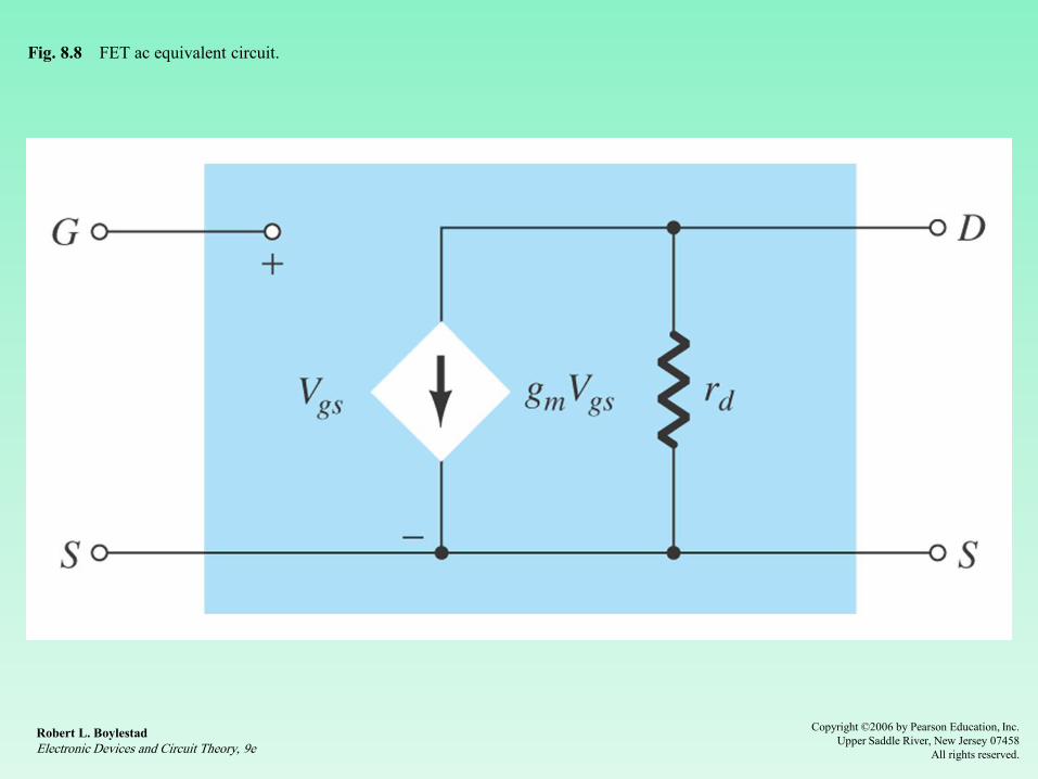
Fig. 8.8 FET ac equivalent circuit.
Robert L. Boylestad
Electronic Devices and Circuit Theory, 9e
Copyright ©2006 by Pearson Education, Inc.
Upper Saddle River, New Jersey 07458
All rights reserved.

Fig. 8.9 FET ac equivalent model for Example 8.6.
Robert L. Boylestad
Electronic Devices and Circuit Theory, 9e
Copyright ©2006 by Pearson Education, Inc.
Upper Saddle River, New Jersey 07458
All rights reserved.

Fig. 8.10 JFET fixed-bias configuration.
Robert L. Boylestad
Electronic Devices and Circuit Theory, 9e
Copyright ©2006 by Pearson Education, Inc.
Upper Saddle River, New Jersey 07458
All rights reserved.

Fig. 8.11 Substituting the JFET ac equivalent circuit unit into the network of Fig. 8.10.
Robert L. Boylestad
Electronic Devices and Circuit Theory, 9e
Copyright ©2006 by Pearson Education, Inc.
Upper Saddle River, New Jersey 07458
All rights reserved.

Fig. 8.12 Redrawn network of Fig. 8.11.
Robert L. Boylestad
Electronic Devices and Circuit Theory, 9e
Copyright ©2006 by Pearson Education, Inc.
Upper Saddle River, New Jersey 07458
All rights reserved.

Fig. 8.13 Determining Zo.
Robert L. Boylestad
Electronic Devices and Circuit Theory, 9e
Copyright ©2006 by Pearson Education, Inc.
Upper Saddle River, New Jersey 07458
All rights reserved.

Fig. 8.14 JFET configuration for Example 8.7.
Robert L. Boylestad
Electronic Devices and Circuit Theory, 9e
Copyright ©2006 by Pearson Education, Inc.
Upper Saddle River, New Jersey 07458
All rights reserved.

Fig. 8.15 Self-bias JFET configuration.
Robert L. Boylestad
Electronic Devices and Circuit Theory, 9e
Copyright ©2006 by Pearson Education, Inc.
Upper Saddle River, New Jersey 07458
All rights reserved.
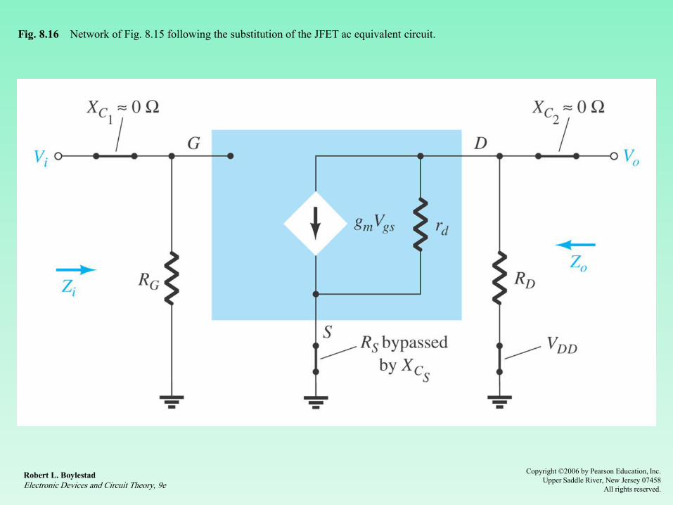
Fig. 8.16 Network of Fig. 8.15 following the substitution of the JFET ac equivalent circuit.
Robert L. Boylestad
Electronic Devices and Circuit Theory, 9e
Copyright ©2006 by Pearson Education, Inc.
Upper Saddle River, New Jersey 07458
All rights reserved.

Fig. 8.17 Redrawn network of Fig. 8.16.
Robert L. Boylestad
Electronic Devices and Circuit Theory, 9e
Copyright ©2006 by Pearson Education, Inc.
Upper Saddle River, New Jersey 07458
All rights reserved.

Fig. 8.18 Self-bias JFET configuration including the effects of RS with rd = ∞ Ω.
Robert L. Boylestad
Electronic Devices and Circuit Theory, 9e
Copyright ©2006 by Pearson Education, Inc.
Upper Saddle River, New Jersey 07458
All rights reserved.

Fig. 8.19 Including the effects of rd in the self-bias JFET configuration.
Robert L. Boylestad
Electronic Devices and Circuit Theory, 9e
Copyright ©2006 by Pearson Education, Inc.
Upper Saddle River, New Jersey 07458
All rights reserved.

Fig. 8.20 Network for Example 8.8.
Robert L. Boylestad
Electronic Devices and Circuit Theory, 9e
Copyright ©2006 by Pearson Education, Inc.
Upper Saddle River, New Jersey 07458
All rights reserved.

Fig. 8.21 Parameters and equations for Example 8.8 using Mathcad.
Robert L. Boylestad
Electronic Devices and Circuit Theory, 9e
Copyright ©2006 by Pearson Education, Inc.
Upper Saddle River, New Jersey 07458
All rights reserved.

Fig. 8.22 JFET voltage-divider configuration.
Robert L. Boylestad
Electronic Devices and Circuit Theory, 9e
Copyright ©2006 by Pearson Education, Inc.
Upper Saddle River, New Jersey 07458
All rights reserved.

Fig. 8.23 Network of Fig. 8.22 under ac conditions.
Robert L. Boylestad
Electronic Devices and Circuit Theory, 9e
Copyright ©2006 by Pearson Education, Inc.
Upper Saddle River, New Jersey 07458
All rights reserved.

Fig. 8.24 Redrawn network of Fig. 8.23.
Robert L. Boylestad
Electronic Devices and Circuit Theory, 9e
Copyright ©2006 by Pearson Education, Inc.
Upper Saddle River, New Jersey 07458
All rights reserved.

Fig. 8.25 JFET source-follower configuration.
Robert L. Boylestad
Electronic Devices and Circuit Theory, 9e
Copyright ©2006 by Pearson Education, Inc.
Upper Saddle River, New Jersey 07458
All rights reserved.

Fig. 8.26 Network of Fig. 8.25 following the substitution of the JFET ac equivalent model.
Robert L. Boylestad
Electronic Devices and Circuit Theory, 9e
Copyright ©2006 by Pearson Education, Inc.
Upper Saddle River, New Jersey 07458
All rights reserved.

Fig. 8.27 Network of Fig. 8.26 redrawn.
Robert L. Boylestad
Electronic Devices and Circuit Theory, 9e
Copyright ©2006 by Pearson Education, Inc.
Upper Saddle River, New Jersey 07458
All rights reserved.

Fig. 8.28 Determining Zo for the network of Fig. 8.25.
Robert L. Boylestad
Electronic Devices and Circuit Theory, 9e
Copyright ©2006 by Pearson Education, Inc.
Upper Saddle River, New Jersey 07458
All rights reserved.

Fig. 8.29 Network to be analyzed in Example 8.9.
Robert L. Boylestad
Electronic Devices and Circuit Theory, 9e
Copyright ©2006 by Pearson Education, Inc.
Upper Saddle River, New Jersey 07458
All rights reserved.

Fig. 8.30 JFET common-gate configuration.
Robert L. Boylestad
Electronic Devices and Circuit Theory, 9e
Copyright ©2006 by Pearson Education, Inc.
Upper Saddle River, New Jersey 07458
All rights reserved.

Fig. 8.31 Network of Fig. 8.30 following substitution of JFET ac equivalent model.
Robert L. Boylestad
Electronic Devices and Circuit Theory, 9e
Copyright ©2006 by Pearson Education, Inc.
Upper Saddle River, New Jersey 07458
All rights reserved.

Fig. 8.32 Determining Z'i for the network of Fig. 8.30.
Robert L. Boylestad
Electronic Devices and Circuit Theory, 9e
Copyright ©2006 by Pearson Education, Inc.
Upper Saddle River, New Jersey 07458
All rights reserved.

Fig. 8.33 Network for Example 8.10.
Robert L. Boylestad
Electronic Devices and Circuit Theory, 9e
Copyright ©2006 by Pearson Education, Inc.
Upper Saddle River, New Jersey 07458
All rights reserved.

Fig. 8.34 D-MOSFET ac equivalent model.
Robert L. Boylestad
Electronic Devices and Circuit Theory, 9e
Copyright ©2006 by Pearson Education, Inc.
Upper Saddle River, New Jersey 07458
All rights reserved.

Fig. 8.35 Network for Example 8.11.
Robert L. Boylestad
Electronic Devices and Circuit Theory, 9e
Copyright ©2006 by Pearson Education, Inc.
Upper Saddle River, New Jersey 07458
All rights reserved.

Fig. 8.36 AC equivalent circuit for Fig. 8.35.
Robert L. Boylestad
Electronic Devices and Circuit Theory, 9e
Copyright ©2006 by Pearson Education, Inc.
Upper Saddle River, New Jersey 07458
All rights reserved.

Fig. 8.37 Enhancement MOSFET ac small-signal model.
Robert L. Boylestad
Electronic Devices and Circuit Theory, 9e
Copyright ©2006 by Pearson Education, Inc.
Upper Saddle River, New Jersey 07458
All rights reserved.

Fig. 8.38 E-MOSFET drain-feedback configuration.
Robert L. Boylestad
Electronic Devices and Circuit Theory, 9e
Copyright ©2006 by Pearson Education, Inc.
Upper Saddle River, New Jersey 07458
All rights reserved.

Fig. 8.39 AC equivalent of the network of Fig. 8.38.
Robert L. Boylestad
Electronic Devices and Circuit Theory, 9e
Copyright ©2006 by Pearson Education, Inc.
Upper Saddle River, New Jersey 07458
All rights reserved.

Fig. 8.40 Determining Zo for the network of Fig. 8.38.
Robert L. Boylestad
Electronic Devices and Circuit Theory, 9e
Copyright ©2006 by Pearson Education, Inc.
Upper Saddle River, New Jersey 07458
All rights reserved.

Fig. 8.41 Drain-feedback amplifier from Example 8.11.
Robert L. Boylestad
Electronic Devices and Circuit Theory, 9e
Copyright ©2006 by Pearson Education, Inc.
Upper Saddle River, New Jersey 07458
All rights reserved.

Fig. 8.42 E-MOSFET voltage-divider configuration.
Robert L. Boylestad
Electronic Devices and Circuit Theory, 9e
Copyright ©2006 by Pearson Education, Inc.
Upper Saddle River, New Jersey 07458
All rights reserved.

Fig. 8.43 AC equivalent network for the configuration of Fig. 8.42.
Robert L. Boylestad
Electronic Devices and Circuit Theory, 9e
Copyright ©2006 by Pearson Education, Inc.
Upper Saddle River, New Jersey 07458
All rights reserved.

Fig. 8.44 Circuit for desired voltage gain in Example 8.13.
Robert L. Boylestad
Electronic Devices and Circuit Theory, 9e
Copyright ©2006 by Pearson Education, Inc.
Upper Saddle River, New Jersey 07458
All rights reserved.

Fig. 8.45 Network for desired voltage gain in Example 8.14.
Robert L. Boylestad
Electronic Devices and Circuit Theory, 9e
Copyright ©2006 by Pearson Education, Inc.
Upper Saddle River, New Jersey 07458
All rights reserved.

Fig. 8.46 JFET amplifier with Rsig and RL.
Robert L. Boylestad
Electronic Devices and Circuit Theory, 9e
Copyright ©2006 by Pearson Education, Inc.
Upper Saddle River, New Jersey 07458
All rights reserved.

Fig. 8.47 Network of Fig. 8.46 following the substitution of the ac equivalent circuit for the JFET.
Robert L. Boylestad
Electronic Devices and Circuit Theory, 9e
Copyright ©2006 by Pearson Education, Inc.
Upper Saddle River, New Jersey 07458
All rights reserved.

Fig. 8.48 Cascaded FET amplifier.
Robert L. Boylestad
Electronic Devices and Circuit Theory, 9e
Copyright ©2006 by Pearson Education, Inc.
Upper Saddle River, New Jersey 07458
All rights reserved.

Fig. 8.49 Cascade amplifier circuit for Example 8.16.
Robert L. Boylestad
Electronic Devices and Circuit Theory, 9e
Copyright ©2006 by Pearson Education, Inc.
Upper Saddle River, New Jersey 07458
All rights reserved.

Fig. 8.50 Cascaded JFET-BJT amplifier for Example 8.17.
Robert L. Boylestad
Electronic Devices and Circuit Theory, 9e
Copyright ©2006 by Pearson Education, Inc.
Upper Saddle River, New Jersey 07458
All rights reserved.

Fig. 8.51 Basic components of a three-channel JFET audio mixer.
Robert L. Boylestad
Electronic Devices and Circuit Theory, 9e
Copyright ©2006 by Pearson Education, Inc.
Upper Saddle River, New Jersey 07458
All rights reserved.

Fig. 8.52 (a) Application of a high- and a low-impedance source to the mixer of Fig. 8.51; (b) reduced equivalent
without the 100-kΩ isolation resistors; (c) reduced equivalent with the 100-kΩ resistors.
Robert L. Boylestad
Electronic Devices and Circuit Theory, 9e
Copyright ©2006 by Pearson Education, Inc.
Upper Saddle River, New Jersey 07458
All rights reserved.

Fig. 8.53 Demonstrating that for parallel signals, the channel with the least internal impedance and most power
controls the situation.
Robert L. Boylestad
Electronic Devices and Circuit Theory, 9e
Copyright ©2006 by Pearson Education, Inc.
Upper Saddle River, New Jersey 07458
All rights reserved.

Fig. 8.54 Battery-powered (9-V), two-station intercom: (a) external appearance; (b) internal construction.
Robert L. Boylestad
Electronic Devices and Circuit Theory, 9e
Copyright ©2006 by Pearson Education, Inc.
Upper Saddle River, New Jersey 07458
All rights reserved.

Fig. 8.55 Noise development due to mechanical switching.
Robert L. Boylestad
Electronic Devices and Circuit Theory, 9e
Copyright ©2006 by Pearson Education, Inc.
Upper Saddle River, New Jersey 07458
All rights reserved.

Fig. 8.56 Silent switching audio network: (a) JFET configuration; (b) with both signals present; (c) with one signal
on.
Robert L. Boylestad
Electronic Devices and Circuit Theory, 9e
Copyright ©2006 by Pearson Education, Inc.
Upper Saddle River, New Jersey 07458
All rights reserved.

Fig. 8.56 (continued) Silent switching audio network: (a) JFET configuration; (b) with both signals present; (c) with
one signal on.
Robert L. Boylestad
Electronic Devices and Circuit Theory, 9e
Copyright ©2006 by Pearson Education, Inc.
Upper Saddle River, New Jersey 07458
All rights reserved.

Fig. 8.56 (continued) Silent switching audio network: (a) JFET configuration; (b) with both signals present; (c) with
one signal on.
Robert L. Boylestad
Electronic Devices and Circuit Theory, 9e
Copyright ©2006 by Pearson Education, Inc.
Upper Saddle River, New Jersey 07458
All rights reserved.

Fig. 8.57 Specification sheet for a low-cost analog JFET current switch. (Copyright of Semiconductor Components
Industries, LLC. Used by permission.)
Robert L. Boylestad
Electronic Devices and Circuit Theory, 9e
Copyright ©2006 by Pearson Education, Inc.
Upper Saddle River, New Jersey 07458
All rights reserved.

Fig. 8.58 Phase-shift networks: (a) advance; (b) retard.
Robert L. Boylestad
Electronic Devices and Circuit Theory, 9e
Copyright ©2006 by Pearson Education, Inc.
Upper Saddle River, New Jersey 07458
All rights reserved.

Fig. 8.59 RC phase-advance network.
Robert L. Boylestad
Electronic Devices and Circuit Theory, 9e
Copyright ©2006 by Pearson Education, Inc.
Upper Saddle River, New Jersey 07458
All rights reserved.

Fig. 8.60 Passive infrared (PIR) motion-detection system.
Robert L. Boylestad
Electronic Devices and Circuit Theory, 9e
Copyright ©2006 by Pearson Education, Inc.
Upper Saddle River, New Jersey 07458
All rights reserved.

Fig. 8.61 Commercially available PIR motion-detection unit: (a) external appearance; (b) internal construction; (c) pet
option coverage.
Robert L. Boylestad
Electronic Devices and Circuit Theory, 9e
Copyright ©2006 by Pearson Education, Inc.
Upper Saddle River, New Jersey 07458
All rights reserved.

Fig. 8.61 (continued) Commercially available PIR motion-detection unit: (a) external appearance; (b) internal
construction; (c) pet option coverage.
Robert L. Boylestad
Electronic Devices and Circuit Theory, 9e
Copyright ©2006 by Pearson Education, Inc.
Upper Saddle River, New Jersey 07458
All rights reserved.

Fig. 8.62 Fixed-bias JFET configuration with an ac source.
Robert L. Boylestad
Electronic Devices and Circuit Theory, 9e
Copyright ©2006 by Pearson Education, Inc.
Upper Saddle River, New Jersey 07458
All rights reserved.

Fig. 8.63 Output file for the network of Fig. 8.62.
Robert L. Boylestad
Electronic Devices and Circuit Theory, 9e
Copyright ©2006 by Pearson Education, Inc.
Upper Saddle River, New Jersey 07458
All rights reserved.

Fig. 8.64 JFET voltage-divider configuration with an ac source.
Robert L. Boylestad
Electronic Devices and Circuit Theory, 9e
Copyright ©2006 by Pearson Education, Inc.
Upper Saddle River, New Jersey 07458
All rights reserved.

Fig. 8.65 The ac drain and gate voltage for the voltage-divider JFET configuration of Fig. 8.64.
Robert L. Boylestad
Electronic Devices and Circuit Theory, 9e
Copyright ©2006 by Pearson Education, Inc.
Upper Saddle River, New Jersey 07458
All rights reserved.

Fig. 8.66 Design Center network for analyzing cascaded JFET amplifiers.
Robert L. Boylestad
Electronic Devices and Circuit Theory, 9e
Copyright ©2006 by Pearson Education, Inc.
Upper Saddle River, New Jersey 07458
All rights reserved.

Fig. 8.67 Display of resulting JFET model definition.
Robert L. Boylestad
Electronic Devices and Circuit Theory, 9e
Copyright ©2006 by Pearson Education, Inc.
Upper Saddle River, New Jersey 07458
All rights reserved.

Fig. 8.68 PSpice output for the network of Fig. 8.66 (edited).
Robert L. Boylestad
Electronic Devices and Circuit Theory, 9e
Copyright ©2006 by Pearson Education, Inc.
Upper Saddle River, New Jersey 07458
All rights reserved.

Fig. 8.69 Display showing dc bias levels.
Robert L. Boylestad
Electronic Devices and Circuit Theory, 9e
Copyright ©2006 by Pearson Education, Inc.
Upper Saddle River, New Jersey 07458
All rights reserved.

Fig. 8.70 JFET self-bias network using Multisim.
Robert L. Boylestad
Electronic Devices and Circuit Theory, 9e
Copyright ©2006 by Pearson Education, Inc.
Upper Saddle River, New Jersey 07458
All rights reserved.

Fig. 8.71 JFET transfer characteristic for Problem 11.
Robert L. Boylestad
Electronic Devices and Circuit Theory, 9e
Copyright ©2006 by Pearson Education, Inc.
Upper Saddle River, New Jersey 07458
All rights reserved.

Fig. 8.72 JFET drain characteristic for Problem 12.
Robert L. Boylestad
Electronic Devices and Circuit Theory, 9e
Copyright ©2006 by Pearson Education, Inc.
Upper Saddle River, New Jersey 07458
All rights reserved.

Fig. 8.73 Fixed-bias amplifier for Problems 17 and 18.
Robert L. Boylestad
Electronic Devices and Circuit Theory, 9e
Copyright ©2006 by Pearson Education, Inc.
Upper Saddle River, New Jersey 07458
All rights reserved.

Fig. 8.74 Problems 19, 21, 22 and 46.
Robert L. Boylestad
Electronic Devices and Circuit Theory, 9e
Copyright ©2006 by Pearson Education, Inc.
Upper Saddle River, New Jersey 07458
All rights reserved.

Fig. 8.75 Self-bias configuration for Problems 20 and 47.
Robert L. Boylestad
Electronic Devices and Circuit Theory, 9e
Copyright ©2006 by Pearson Education, Inc.
Upper Saddle River, New Jersey 07458
All rights reserved.

Fig. 8.76 Problems 23 to 26 and 48.
Robert L. Boylestad
Electronic Devices and Circuit Theory, 9e
Copyright ©2006 by Pearson Education, Inc.
Upper Saddle River, New Jersey 07458
All rights reserved.

Fig. 8.77 Problems 27 and 28.
Robert L. Boylestad
Electronic Devices and Circuit Theory, 9e
Copyright ©2006 by Pearson Education, Inc.
Upper Saddle River, New Jersey 07458
All rights reserved.

Fig. 8.78 Problem 29.
Robert L. Boylestad
Electronic Devices and Circuit Theory, 9e
Copyright ©2006 by Pearson Education, Inc.
Upper Saddle River, New Jersey 07458
All rights reserved.

Fig. 8.79 Problems 30, 31, and 49.
Robert L. Boylestad
Electronic Devices and Circuit Theory, 9e
Copyright ©2006 by Pearson Education, Inc.
Upper Saddle River, New Jersey 07458
All rights reserved.

Fig. 8.80 Problem 32.
Robert L. Boylestad
Electronic Devices and Circuit Theory, 9e
Copyright ©2006 by Pearson Education, Inc.
Upper Saddle River, New Jersey 07458
All rights reserved.

Fig. 8.81 Problem 33.
Robert L. Boylestad
Electronic Devices and Circuit Theory, 9e
Copyright ©2006 by Pearson Education, Inc.
Upper Saddle River, New Jersey 07458
All rights reserved.

Fig. 8.82 Problems 34, 35, and 50.
Robert L. Boylestad
Electronic Devices and Circuit Theory, 9e
Copyright ©2006 by Pearson Education, Inc.
Upper Saddle River, New Jersey 07458
All rights reserved.

Fig. 8.83 Problem 36.
Robert L. Boylestad
Electronic Devices and Circuit Theory, 9e
Copyright ©2006 by Pearson Education, Inc.
Upper Saddle River, New Jersey 07458
All rights reserved.

Fig. 8.84 Problem 37.
Robert L. Boylestad
Electronic Devices and Circuit Theory, 9e
Copyright ©2006 by Pearson Education, Inc.
Upper Saddle River, New Jersey 07458
All rights reserved.

Fig. 8.85 Problems 39, 40, and 51.
Robert L. Boylestad
Electronic Devices and Circuit Theory, 9e
Copyright ©2006 by Pearson Education, Inc.
Upper Saddle River, New Jersey 07458
All rights reserved.

Fig. 8.86 Problems 41 and 42.
Robert L. Boylestad
Electronic Devices and Circuit Theory, 9e
Copyright ©2006 by Pearson Education, Inc.
Upper Saddle River, New Jersey 07458
All rights reserved.

Fig. 8.87 Problem 43.
Robert L. Boylestad
Electronic Devices and Circuit Theory, 9e
Copyright ©2006 by Pearson Education, Inc.
Upper Saddle River, New Jersey 07458
All rights reserved.

Fig. 8.88 Problem 44.
Robert L. Boylestad
Electronic Devices and Circuit Theory, 9e
Copyright ©2006 by Pearson Education, Inc.
Upper Saddle River, New Jersey 07458
All rights reserved.

Fig. 8.89 Problem 45.
Robert L. Boylestad
Electronic Devices and Circuit Theory, 9e
Copyright ©2006 by Pearson Education, Inc.
Upper Saddle River, New Jersey 07458
All rights reserved.

Fig. 8.90 Problem 46.
Robert L. Boylestad
Electronic Devices and Circuit Theory, 9e
Copyright ©2006 by Pearson Education, Inc.
Upper Saddle River, New Jersey 07458
All rights reserved.

Fig. 8.91 Problem 47.
Robert L. Boylestad
Electronic Devices and Circuit Theory, 9e
Copyright ©2006 by Pearson Education, Inc.
Upper Saddle River, New Jersey 07458
All rights reserved.

Fig. 8.92 Problem 48.
Robert L. Boylestad
Electronic Devices and Circuit Theory, 9e
Copyright ©2006 by Pearson Education, Inc.
Upper Saddle River, New Jersey 07458
All rights reserved.

Fig. 8.93 Problems 49 to 53.
Robert L. Boylestad
Electronic Devices and Circuit Theory, 9e
Copyright ©2006 by Pearson Education, Inc.
Upper Saddle River, New Jersey 07458
All rights reserved.

Fig. 8.94 Problems 54 to 56.
Robert L. Boylestad
Electronic Devices and Circuit Theory, 9e
Copyright ©2006 by Pearson Education, Inc.
Upper Saddle River, New Jersey 07458
All rights reserved.