Embed Size (px)
Citation preview
Deformable mirror device spatial light modulators andtheir applicability to optical neural networks
Dean R. Collins, Jeffrey B. Sampsell, Larry J. Hornbeck, James M. Florence, P. Andrew Penz, andMichael T. Gately
All neural networks are characterized by a large number of interconnections between processor nodes. Ingeneral, the value of these interconnections (weights) must be modifiable. However, current semiconductortechnology does not lend itself well to modifiable interconnection technology. A novel type of spatial lightmodulator, the deformable mirror device, is proposed as the breakthrough needed to solve the neural networkinterconnect problem.
1. Neural Network Overview
A neural network (NN) architecture is a fine-grained parallel architecture with simple processorscoupled at long range to the input. Neural networksexecute matrix and signal processing type operations.They recognize and reorganize by correlating inputswith learned states. They have the ability to clusterstored information, be trained rather than pro-grammed, and to recall information when the inquiryis both incomplete and erroneous. Of the severaltypes of neural network, some of the better known areHopfield,1 backpropagation (Rumelhart et al.),2 BSB(Anderson et al.),3 and ART (Grossberg).4
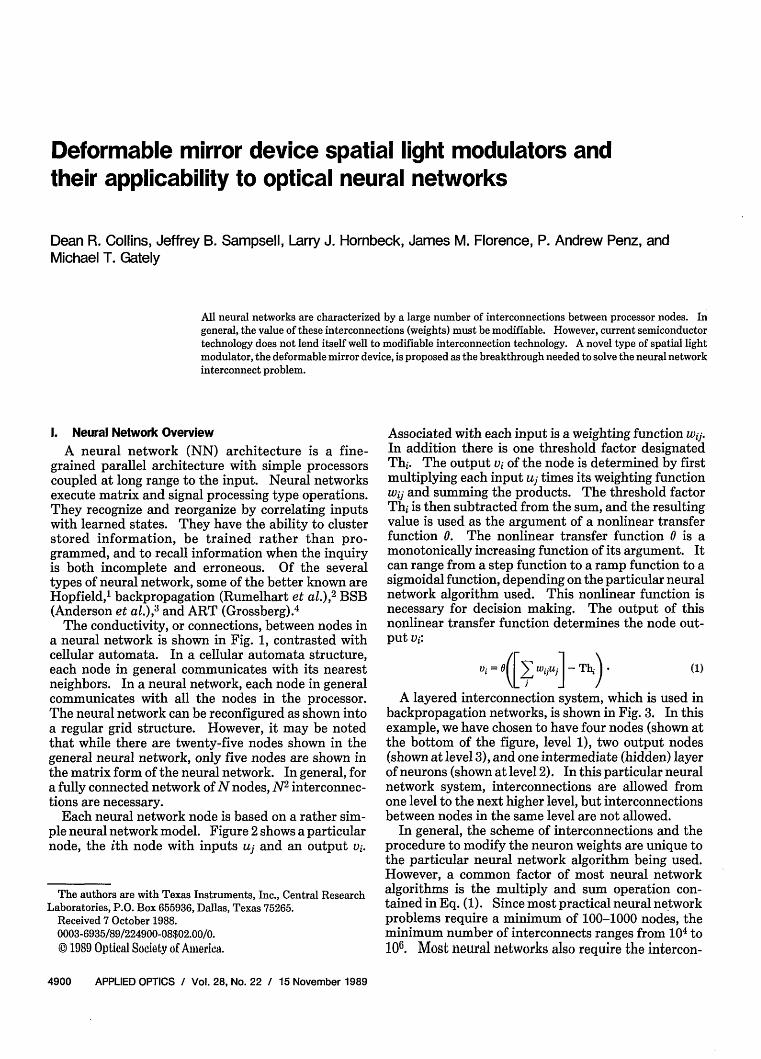
The conductivity, or connections, between nodes ina neural network is shown in Fig. 1, contrasted withcellular automata. In a cellular automata structure,each node in general communicates with its nearestneighbors. In a neural network, each node in generalcommunicates with all the nodes in the processor.The neural network can be reconfigured as shown intoa regular grid structure. However, it may be notedthat while there are twenty-five nodes shown in thegeneral neural network, only five nodes are shown inthe matrix form of the neural network. In general, fora fully connected network of N nodes, N2 interconnec-tions are necessary.
Each neural network node is based on a rather sim-ple neural network model. Figure 2 shows a particularnode, the ith node with inputs uj and an output vi.
The authors are with Texas Instruments, Inc., Central ResearchLaboratories, P.O. Box 655936, Dallas, Texas 75265.
Received 7 October 1988.0003-6935/89/224900-08$02.00/0.
© 1989 Optical Society of America.
Associated with each input is a weighting function wij.In addition there is one threshold factor designatedThi. The output vi of the node is determined by firstmultiplying each input uj times its weighting functionwij and summing the products. The threshold factorThi is then subtracted from the sum, and the resultingvalue is used as the argument of a nonlinear transferfunction 0. The nonlinear transfer function 0 is amonotonically increasing function of its argument. Itcan range from a step function to a ramp function to asigmoidal function, depending on the particular neuralnetwork algorithm used. This nonlinear function isnecessary for decision making. The output of thisnonlinear transfer function determines the node out-put vi:
Vi = ([ Wij~] -Tbe). (1)
A layered interconnection system, which is used inbackpropagation networks, is shown in Fig. 3. In thisexample, we have chosen to have four nodes (shown atthe bottom of the figure, level 1), two output nodes(shown at level 3), and one intermediate (hidden) layerof neurons (shown at level 2). In this particular neuralnetwork system, interconnections are allowed fromone level to the next higher level, but interconnectionsbetween nodes in the same level are not allowed.
In general, the scheme of interconnections and theprocedure to modify the neuron weights are unique tothe particular neural network algorithm being used.However, a common factor of most neural networkalgorithms is the multiply and sum operation con-tained in Eq. (1). Since most practical neural networkproblems require a minimum of 100-1000 nodes, theminimum number of interconnects ranges from 104 to106. Most neural networks also require the intercon-
4900 APPLIED OPTICS / Vol. 28, No. 22 / 15 November 1989
Output
Fig. 1. Conductivity of neural network and cellular automata.
U1 U2 U3 U4Input
Fig. 3. Layered neural network system.
Beam (Aluminum Allov)
Spacer-
Plasma Et(:h Access Holes
" Isotropic Plasma-Etch Profile
-Etch Stop (i 2)
Fig. 2. Neural network model and nonlinear transfer function.
nections (weights) to have analog values. Further-more, for learning to take place, these interconnectsmust be modifiable. The large number, analog values,and variable nature of the interconnects pose an ex-treme challenge for conventional semiconductor tech-nology.
11. Spatial Light Modulators
Since the number of interconnections of a neuralnetwork is perceived to be the limiting factor, it isnatural to advocate optical technology to solve theinterconnect problem. It is very easy to make complexoptical interconnections, since light beams passthrough each other. However, it is very difficult tobuild a light switch. Light switches, or 2-D arrays oflight switches called spatial light modulators (SLMs),exist and have been used by Farhat et al.,5 Psaltis andFarhat, 6 Anderson,7 and others to build optical neuralnetworks. These systems were either very expensive,slow, or tied to TV format. In general, these systemswere quite limited by the performance of the SLM.Several holographic techniques using film have beendemonstrated, but they suffer from the inability tovary the interconnections.
We describe both a novel type of spatial light modu-lator, called the deformable mirror device (DMD),-11and its applicability to neural network computation. 1 2 l 4
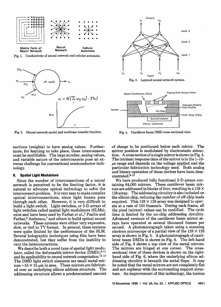
The DMD light switch elements are small metal mir-rors -15 X 15 jim in area. These mirrors are fabricat-ed over an underlying silicon address structure. Theaddressing structure allows a predetermined amount
Fig. 4. Cantilever beam DMD cross-sectional view.
of charge to be positioned below each mirror. Themirror position is modulated by electrostatic attrac-tion. A cross section of a single mirror is shown in Fig. 4.The intrinsic response time of the mirror is in the 1-10-gs range and depends on the voltage applied and theparticular fabrication technology used. Both analogand binary operation of these devices have been dem-onstrated.8 11
We have produced fully functional 2-D arrays con-taining 64,000 mirrors. These cantilever beam mir-rors are addressed in blocks of four, resulting in a 128 X128 array. The addressing circuitry is also included onthe silicon chip, reducing the number of off-chip leadsrequired. This 128 X 128 array was designed to oper-ate at a rate of 150 frames/s. During each frame, allthe pixel (mirror) values can be modified. The cycletime is limited by the on-chip addressing circuitry.Advanced versions of the cantilever beam mirror ar-rays have operated at several thousand frames persecond. A photomicrograph taken using a scanningelectron microscope of a partial view of the 128 X 128array is shown in Fig. 5. A photomicrograph of canti-lever beam DMDs is shown in Fig. 6. The left-handside of Fig. 6 shows a top view of the metal mirrors.The mirrors are hinged at one corner. The cross-sectional view of these devices is shown on the right-hand side of Fig. 6, where the underlying silicon ad-dressing circuitry is beneath the metal flaps. It maybe noted that the metal mirrors are not completely flatand not coplanar with the surrounding support struc-ture. An improvement of this technology, the torsion
15 November 1989 / Vol. 28, No. 22 / APPLIED OPTICS 4901
Matrix Form ofNeural Network
* * 0 0
* 0 * 0 0
CellularAutomata
NeuralNetwork
Thi
Uj
Level 3
Level 2
Level 1
V,
Ul
Ofx)
Vi = 0([Wi uj] -Th)J
x
Hge/iB2X///l 1.'¢/I
\ \Air G a[ Buried Imp
Silicon Substrate
_
NIIII
. 0
---
0-- -
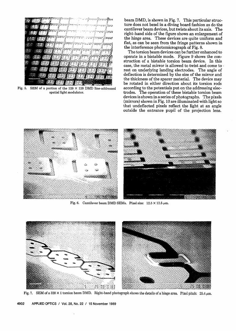
Fig. 5. SEM of a portion of the 128 X 128 DMD line-addressedspatial light modulator.
beam DMD, is shown in Fig. 7. This particular struc-ture does not bend in a diving board fashion as do thecantilever beam devices, but twists about its axis. Theright-hand side of the figure shows an enlargement ofthe hinge area. These devices are quite uniform andflat, as can be seen from the fringe patterns shown inthe interference photomicrograph of Fig. 8.
The torsion beam devices can be further enhanced tooperate in a bistable mode. Figure 9 shows the con-struction of a bistable torsion beam device. In thiscase, the metal mirror is allowed to twist and come torest on underlying landing electrodes. The angle ofdeflection is determined by the size of the mirror andthe thickness of the spacer material. The device maybe rotated in either direction about its torsion rodsaccording to the potentials put on the addressing elec-trodes. The operation of these bistable torsion beamdevices is shown in a series of photographs. The pixels(mirrors) shown in Fig. 10 are illuminated with light sothat undeflected pixels reflect the light at an angleoutside the entrance pupil of the projection lens.
Fig. 6. Cantilever beam DMD SEMs. Pixel size: 12.5 X 12.5 Am.
Fig. 7. SEM of a 320 X 1 torsion beam DMD. Right-hand photograph shows the details of a hinge area. Pixel pitch: 25.4 ,m.
4902 APPLIED OPTICS / Vol. 28, No. 22 / 15 November 1989
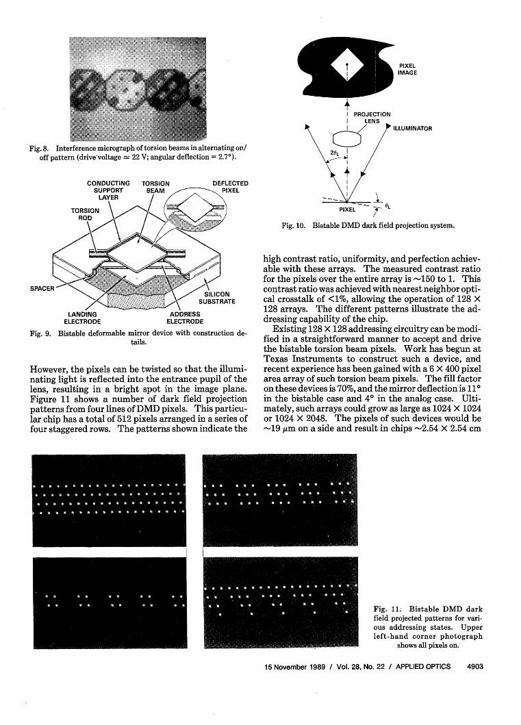
Fig. 8. Interference micrograph of torsion beams in alternating on/off pattern (drive voltage 22 V; angular deflection = 2.7°).
DEFLECTEDAs PIXEL
SPACER- 2
SBSTRATE
LANDING ADDRESSELECTRODE ELECTRODE
Fig. 9. Bistable deformable mirror device with construction de-tails.
However, the pixels can be twisted so that the illumi-nating light is reflected into the entrance pupil of thelens, resulting in a bright spot in the image plane.Figure 11 shows a number of dark field projectionpatterns from four lines of DMD pixels. This particu-lar chip has a total of 512 pixels arranged in a series offour staggered rows. The patterns shown indicate the
Tj P PIXELIMAGE
I PROJECTIONI LENS
/ / ILLUMINATOR
C/20L I
PIXEL OL
Fig. 10. Bistable DMD dark field projection system.
high contrast ratio, uniformity, and perfection achiev-able with these arrays. The measured contrast ratiofor the pixels over the entire array is -150 to 1. Thiscontrast ratio was achieved with nearest neighbor opti-cal crosstalk of <1%, allowing the operation of 128 X128 arrays. The different patterns illustrate the ad-dressing capability of the chip.
Existing 128 X 128 addressing circuitry can be modi-fied in a straightforward manner to accept and drivethe bistable torsion beam pixels. Work has begun atTexas Instruments to construct such a device, andrecent experience has been gained with a 6 X 400 pixelarea array of such torsion beam pixels. The fill factoron these devices is 70%, and the mirror deflection is 110in the bistable case and 40 in the analog case. Ulti-mately, such arrays could grow as large as 1024 X 1024or 1024 X 2048. The pixels of such devices would be-19 /.tm on a side and result in chips -2.54 X 2.54 cm
Fig. 11. Bistable DMD darkfield projected patterns for vari-ous addressing states. Upperleft-hand corner photograph
shows all pixels on.
15 November 1989 / Vol. 28, No. 22 / APPLIED OPTICS 4903
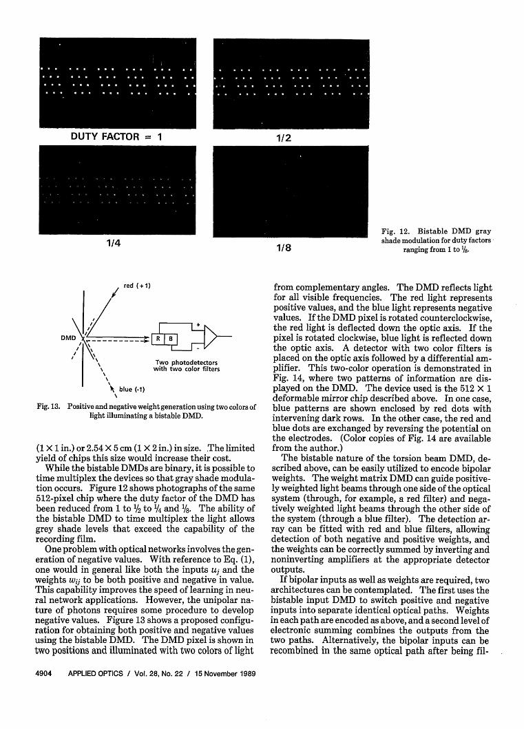
DUTY FACTOR = 1
1/4 1/8
red (+1)
DMD
Two photodetectorswith two color filters
Fig. 13. Positive and negative weight generation using two colors oflight illuminating a bistable DMD.
(1 X 1 in.) or 2.54 X 5 cm (1 X 2 in.) in size. The limitedyield of chips this size would increase their cost.
While the bistable DMDs are binary, it is possible totime multiplex the devices so that gray shade modula-tion occurs. Figure 12 shows photographs of the same512-pixel chip where the duty factor of the DMD hasbeen reduced from 1 to /2 to 1/4 and /8. The ability ofthe bistable DMD to time multiplex the light allowsgrey shade levels that exceed the capability of therecording film.
One problem with optical networks involves the gen-eration of negative values. With reference to Eq. (1),one would in general like both the inputs uj and theweights wij to be both positive and negative in value.This capability improves the speed of learning in neu-ral network applications. However, the unipolar na-ture of photons requires some procedure to developnegative values. Figure 13 shows a proposed configu-ration for obtaining both positive and negative valuesusing the bistable DMD. The DMD pixel is shown intwo positions and illuminated with two colors of light
Fig. 12. Bistable DMD grayshade modulation for duty factors
ranging from 1 to 1/8.
* complementary angles. The DMD reflects light11 visible frequencies. The red light represents;ive values, and the blue light represents negatives. If the DMD pixel is rotated counterclockwise,
red light is deflected down the optic axis. If thel is rotated clockwise, blue light is reflected down)ptic axis. A detector with two color filters ised on the optic axis followed by a differential am-er. This two-color operation is demonstrated in14, where two patterns of information are dis-A on the DMD. The device used is the 512 X 1mable mirror chip described above. In one case,patterns are shown enclosed by red dots withvening dark rows. In the other case, the red anddots are exchanged by reversing the potential onlectrodes. (Color copies of Fig. 14 are availablethe author.).e bistable nature of the torsion beam DMD, de-ed above, can be easily utilized to encode bipolarits. The weight matrix DMD can guide positive-ighted light beams through one side of the opticalm (through, for example, a red filter) and nega-y weighted light beams through the other side ofystem (through a blue filter). The detection ar-an be fitted with red and blue filters, allowing:tion of both negative and positive weights, andeights can be correctly summed by inverting andaverting amplifiers at the appropriate detectorits.bipolar inputs as well as weights are required, twoiectures can be contemplated. The first uses theAe input DMD to switch positive and negatives into separate identical optical paths. Weights:h path are encoded as above, and a second level ofronic summing combines the outputs from thepaths. Alternatively, the bipolar inputs can beibined in the same optical path after being fil-
4904 APPLIED OPTICS / Vol. 28, No. 22 / 15 November 1989
1/2
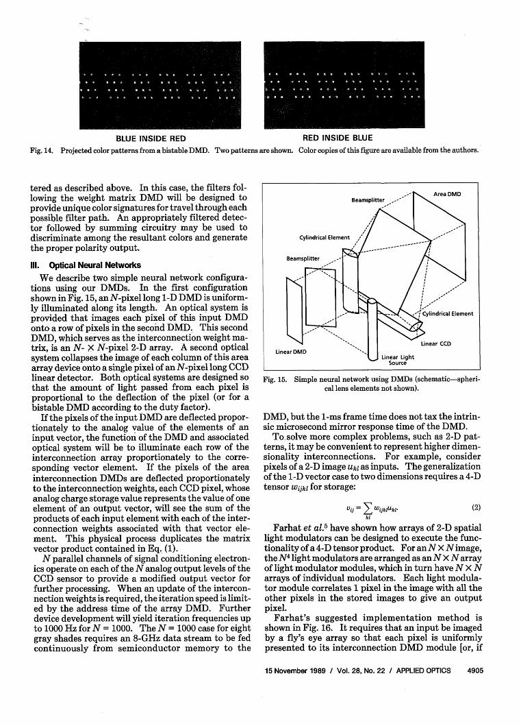
Fig. 14. Projected color patterns from a bistable DMD. Two patterns are shown. Color copies of this figure are available from the authors.
tered as described above. In this case, the filters fol-lowing the weight matrix DMD will be designed toprovide unique color signatures for travel through eachpossible filter path. An appropriately filtered detec-tor followed by summing circuitry may be used todiscriminate among the resultant colors and generatethe proper polarity output.
Ill. Optical Neural Networks
We describe two simple neural network configura-tions using our DMDs. In the first configurationshown in Fig. 15, an N-pixel long 1-D DMD is uniform-ly illuminated along its length. An optical system isprovided that images each pixel of this input DMDonto a row of pixels in the second DMD. This secondDMD, which serves as the interconnection weight ma-trix, is an N- X N-pixel 2-D array. A second opticalsystem collapses the image of each column of this areaarray device onto a single pixel of an N-pixel long CCDlinear detector. Both optical systems are designed sothat the amount of light passed from each pixel isproportional to the deflection of the pixel (or for abistable DMD according to the duty factor).
If the pixels of the input DMD are deflected propor-tionately to the analog value of the elements of aninput vector, the function of the DMD and associatedoptical system will be to illuminate each row of theinterconnection array proportionately to the corre-sponding vector element. If the pixels of the areainterconnection DMDs are deflected proportionatelyto the interconnection weights, each CCD pixel, whoseanalog charge storage value represents the value of oneelement of an output vector, will see the sum of theproducts of each input element with each of the inter-connection weights associated with that vector ele-ment. This physical process duplicates the matrixvector product contained in Eq. (1).
N parallel channels of signal conditioning electron-ics operate on each of the N analog output levels of theCCD sensor to provide a modified output vector forfurther processing. When an update of the intercon-nection weights is required, the iteration speed is limit-ed by the address time of the array DMD. Furtherdevice development will yield iteration frequencies upto 1000 Hz for N = 1000. The N = 1000 case for eightgray shades requires an 8-GHz data stream to be fedcontinuously from semiconductor memory to the
U Linear LightSource
Fig. 15. Simple neural network using DMDs (schematic-spheri-cal lens elements not shown).
DMD, but the 1-ms frame time does not tax the intrin-sic microsecond mirror response time of the DMD.
To. solve more complex problems, such as 2-D pat-terns, it may be convenient to represent higher dimen-sionality interconnections. For example, considerpixels of a 2-D image ukl as inputs. The generalizationof the 1-D vector case to two dimensions requires a 4-Dtensor Wijkl for storage:
(2)Vij = E WijklUkl-ki
Farhat et al.5 have shown how arrays of 2-D spatiallight modulators can be designed to execute the func-tionality of a 4-D tensor product. For an N X N image,the N 4 light modulators are arranged as an N X N arrayof light modulator modules, which in turn have N X Narrays of individual modulators. Each light modula-tor module correlates 1 pixel in the image with all theother pixels in the stored images to give an outputpixel.
Farhat's suggested implementation method isshown in Fig. 16. It requires that an input be imagedby a fly's eye array so that each pixel is uniformlypresented to its interconnection DMD module [or, if
15 November 1989 / Vol. 28, No. 22 / APPLIED OPTICS 4905
BLUE INSIDE RED RED INSIDE BLUE
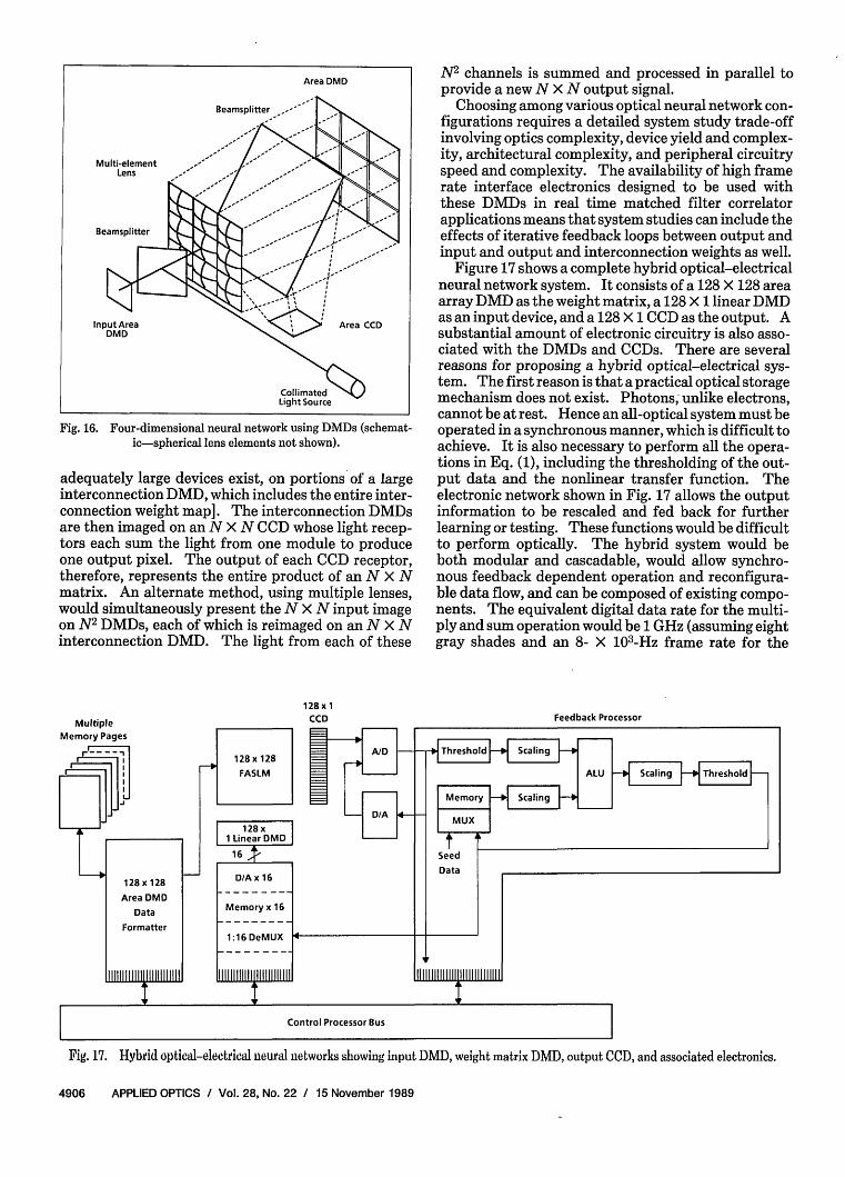
Fig. 16. Four-dimensional neural network using DMDs (schemat-ic-spherical lens elements not shown).
adequately large devices exist, on portions of a largeinterconnection DMD, which includes the entire inter-connection weight map]. The interconnection DMDsare then imaged on an N X N CCD whose light recep-tors each sum the light from one module to produceone output pixel. The output of each CCD receptor,therefore, represents the entire product of an N X Nmatrix. An alternate method, using multiple lenses,would simultaneously present the N X N input imageon N2 DMDs, each of which is reimaged on an N X Ninterconnection DMD. The light from each of these
N2 channels is summed and processed in parallel toprovide a new N X N output signal.
Choosing among various optical neural network con-figurations requires a detailed system study trade-offinvolving optics complexity, device yield and complex-ity, architectural complexity, and peripheral circuitryspeed and complexity. The availability of high framerate interface electronics designed to be used withthese DMDs in real time matched filter correlatorapplications means that system studies can include theeffects of iterative feedback loops between output andinput and output and interconnection weights as well.
Figure 17 shows a complete hybrid optical-electricalneural network system. It consists of a 128 X 128 areaarray DMD as the weight matrix, a 128 X 1 linear DMDas an input device, and a 128 X 1 CCD as the output. Asubstantial amount of electronic circuitry is also asso-ciated with the DMDs and CCDs. There are severalreasons for proposing a hybrid optical-electrical sys-tem. The first reason is that a practical optical storagemechanism does not exist. Photons, unlike electrons,cannot be at rest. Hence an all-optical system must beoperated in a synchronous manner, which is difficult toachieve. It is also necessary to perform all the opera-tions in Eq. (1), including the thresholding of the out-put data and the nonlinear transfer function. Theelectronic network shown in Fig. 17 allows the outputinformation to be rescaled and fed back for furtherlearning or testing. These functions would be difficultto perform optically. The hybrid system would beboth modular and cascadable, would allow synchro-nous feedback dependent operation and reconfigura-ble data flow, and can be composed of existing compo-nents. The equivalent digital data rate for the multi-ply and sum operation would be 1 GHz (assuming eightgray shades and an 8- X 103-Hz frame rate for the
128 x 1CCD Feedback Processor
Fig. 17. Hybrid optcal-eledtkal ueural networks showing input DMD, weight matrix DMD, output CCD, and associated electronics.
4906 APPLIED OPTICS / Vol. 28, No. 22 / 15 November 1989
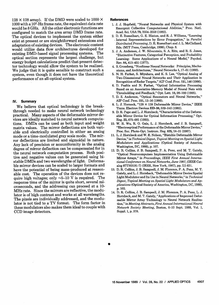
128 X 128 array). If the DMD were scaled to 1000 X1000 with a 103-Hz frame rate, the equivalent data ratewould be 8 GHz. All the other electronic functions areconfigured to match the area array DMD frame rate.The optical devices to implement the system eitherexist at present or are straightforward extensions andadaptation of existing devices. The electronic contentwould utilize data flow architectures developed forexisting DMD-based signal processing systems. Theoptical section represents the largest challenge, butenergy budget calculations predict that present detec-tor technology would allow the system to be realized.We judge that it is quite sensible to construct such asystem, even though it does not have the theoreticalperformance of an all-optical system.
IV. Summary
We believe that optical technology is the break-through needed to make neural network technologypractical. Many aspects of the deformable mirror de-vices are ideally matched to neural network computa-tions. DMDs can be used as both input and weightmatrix values. The mirror deflections are both vari-able and electrically controlled in either an analogmode or a time-modulated gray scale mode. The mir-ror deflections are limited and sigmoidal in nature.Any lack of precision or nonuniformity in the analogdegree of mirror deflection can be compensated for inthe neural network computation process. Both posi-tive and negative values can be generated using bi-stable DMDs and two wavelengths of light. Deforma-ble mirror devices can be scaled to larger formats andhave the potential of being mass-produced at reason-able cost. The operation of the devices does not re-quire high voltages; only -5-10 V is required. Theresponse time of the mirror is quite short, several mi-croseconds, and the addressing can proceed at a 10-MHz rate. Since the mirrors are reflective, the modu-lator is of high contrast and works at all wavelengths.The pixels are individually addressed, and the modu-lator is not tied to a TV format. The form factor inthese modulators also makes them ideal to couple withCCD image detectors.
References1. J. J. Hopfield, "Neural Networks and Physical System with
Emergent Collective Computational Abilities," Proc. Natl.Acad. Sci. USA 79, 2554-2558 (1982).
2. D. E. Rumelhart, G. E. Hinton, and R. J. Williams, "LearningInternal Representations by Error Propagation," in ParallelDistributed Processing, D. E. Rumelhart and J. L. McClelland,Eds. (MIT Press, Cambridge, 1986), Chap. 8.
3. J. A. Anderson, J. W. Silverstein, S. A. Ritz, and R. S. Jones,"Distinctive Features, Categorical Perception, and ProbabilityLearning: Some Applications of a Neural Model," Psychol.Rev. 84,413-451 (1977).
4. S. Grossberg, "Nonlinear Neural Networks: Principles, Mecha-nisms, and Architectures," Neural Networks 1, 17-61 (1988).
5. N. H. Farhat, S. Miyahara, and K. S. Lee, "Optical Analog ofTwo-Dimensional Neural Networks and Their Application inRecognition of Radar Targets," AIP Conf. Proc. 151,146 (1986).
6. D. Psaltis and N. Farhat, "Optical Information ProcessingBased on an Associative-Memory Model of Neural Nets withThresholding and Feedback," Opt. Lett. 10, 98-100 (1985).
7. D. Z. Anderson, "Optical Resonators and Neural Networks,"AIP Conf. Proc. 151, 12-16 (1986).
8. L. J. Horneck, "128 X 128 Deformable Mirror Device," IEEETrans. Electron Devices ED-30, 539-545 (1983).
9. D. R. Pape and L. J. Hornbeck, "Characteristics of the Deform-able Mirror Device for Optical Information Processing," Opt.Eng. 22, 675-681 (1983).
10. W. R. Wu, R. 0. Gale, L. J. Hornbeck, and J. B. Sampsell,"Electrooptical Performance of the Deformable Mirror Device,"Proc. Soc. Photo-Opt. Instrum. Eng. 825, 24-31 (1987).
11. L. J. Hornbeck and W. E. Nelson, "Bistable Deformable MirrorDevice," in Technical Digest, Topical Meeting on Spatial LightModulators and Applications (Optical Society of America,Washington, DC, 1988), p. 107.
12. D. R. Collins, J. B. Sampsell, P. A. Penz, and M. T. Gately,"Optical Neurocomputers Implementation Using DeformableMirror Arrays," in Proceedings, IEEE First Annual Interna-tional Conference on Neural Networks, June 1987, (IEEE Cat-alog 87TH0191-7) (IEEE, New York, 1987), pp. II-631.
13. D. R. Collins, J. B. Sampsell, J. M. Florence, P. A. Penz, M. T.Gately, and L. J. Hornbeck, "Deformable Mirror Device SpatialLight Modulator and Its Use in Neural Networks," in TechnicalDigest, Topical Meeting on Spatial Light Modulators and Ap-plications (Optical Society of America, Washington, DC, 1988),p. 102.
14. D. R. Collins, J. B. Sampsell, J. M. Florence, P. A. Penz, L. J.Hornbeck, and M. T. Gately, "Applications of Improved Defor-mable Mirror Array Technology to Neural Network Realiza-tion," in Meeting Abstracts, First Annual International NeuralNetwork Society Meeting, Boston, 6-10 Sept. 1988, Vol. 1,Suppl. 1, p. 378.
15 November 1989 / Vol. 28, No. 22 / APPLIED OPTICS 4907


![Vega: Nonlinear FEM Deformable Object Simulatorrun.usc.edu/vega/SinSchroederBarbic2012.pdf · Vega: Nonlinear FEM Deformable Object Simulator ... (CalculiX [DW]) deformable ... J](https://img.pdfslide.net/doc/110x75/5aecb8f27f8b9a3b2e8f8865/vega-nonlinear-fem-deformable-object-nonlinear-fem-deformable-object-simulator.jpg)