Embed Size (px)
Citation preview
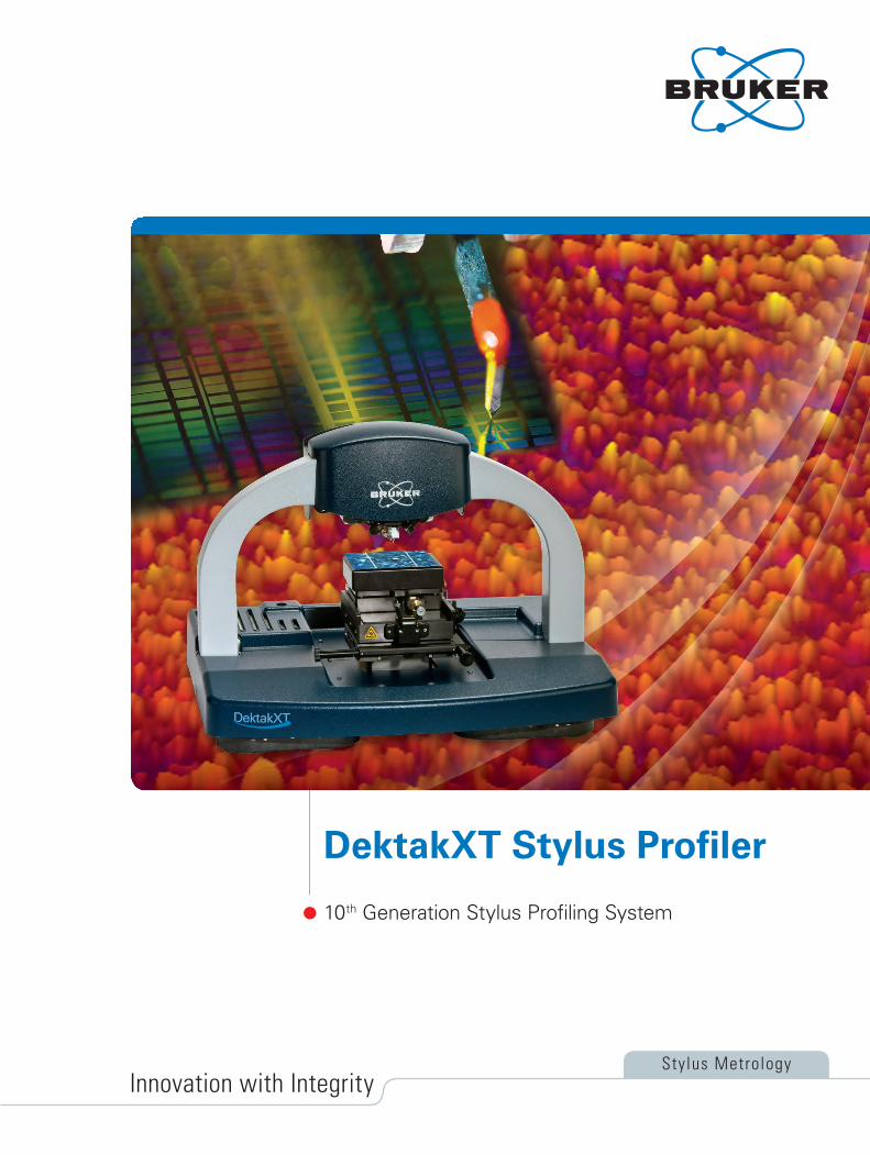
DektakXT Stylus Profiler
10th Generation Stylus Profiling System
Stylus MetrologyInnovation with Integrity
Bruker’s DektakXT™ Stylus Profiler features a revolutionary design that enables 4 angstrom repeatability. This major milestone in stylus profiler performance is the culmination of forty years of Dektak® innovation and industry leadership. Through its combination of industry firsts, DektakXT delivers the ultimate in performance, ease of use and value to enable better process monitoring from R&D to QC. The technological breakthroughs incorporated in Dektak enable critical nanometer-level surface measurements for the microelectronics, semiconductor, solar, high-brightness LED, medical, and materials science industries.
DektakXT Delivers
■ Unmatched performance
– 4Å repeatability delivers industry-leading accuracy
– Single-arch design provides breakthrough scan stability
– Leading-edge “smart electronics” establish new low noise benchmark
– New hardware configuration offers 40% faster data collection times than prior generations
– 64-bit, parallel processing Vision64 software architecture delivers up to 10 times faster data analyses
■ Unprecedented efficiency and ease of use
– Intuitive Vision64™ user interface workflow simplifies operation
– Self-aligning styli enables effortless tip exchange
■ Incomparable value from the world leader in stylus profilers
– Bruker delivers premier performance in an affordable package
– Single sensor design offers low force and extended range in a single platform
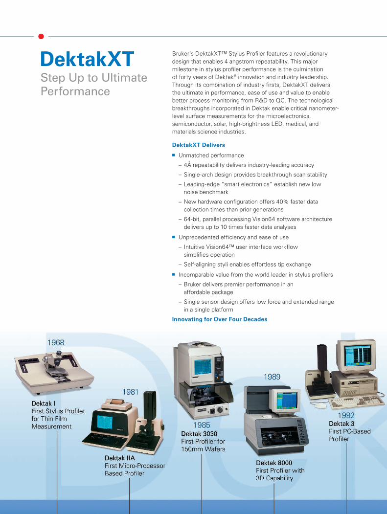
Innovating for Over Four Decades
Step Up to Ultimate Performance
DektakXT
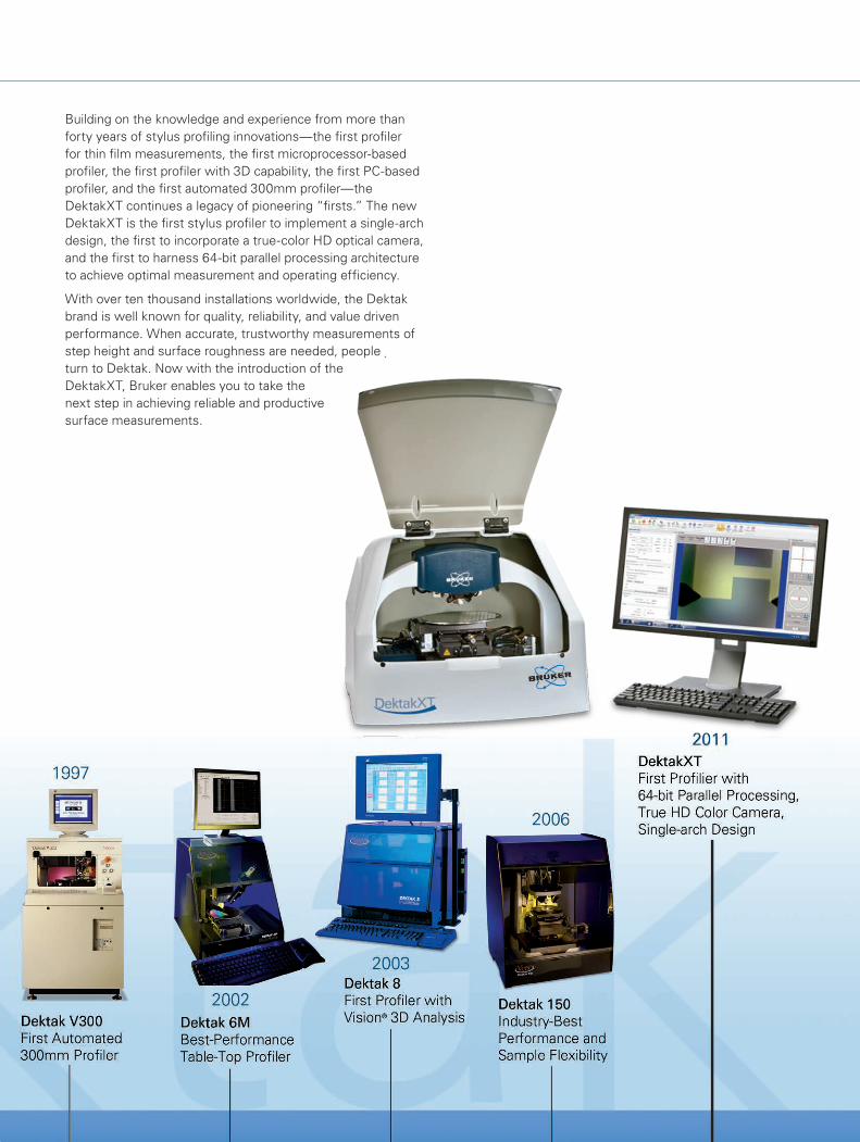
Building on the knowledge and experience from more than forty years of stylus profiling innovations—the first profiler for thin film measurements, the first microprocessor-based profiler, the first profiler with 3D capability, the first PC-based profiler, and the first automated 300mm profiler—the DektakXT continues a legacy of pioneering “firsts.” The new DektakXT is the first stylus profiler to implement a single-arch design, the first to incorporate a true-color HD optical camera, and the first to harness 64-bit parallel processing architecture to achieve optimal measurement and operating efficiency.
With over ten thousand installations worldwide, the Dektak brand is well known for quality, reliability, and value driven performance. When accurate, trustworthy measurements of step height and surface roughness are needed, people turn to Dektak. Now with the introduction of the DektakXT, Bruker enables you to take the next step in achieving reliable and productive surface measurements.
Stylus system performance is characterized by three fundamental factors: measurement repeatability, time to results, and ease of use. These factors directly correlate to the quality of data and operator efficiency. The DekatkXT utilizes revolutionary architecture and best-in-class software to address all three factors to achieve ultimate performance.
Delivering Repeatable Measurements
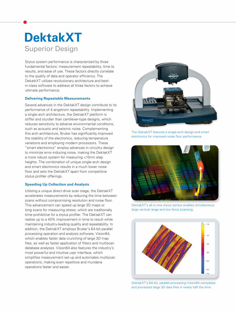
Several advances in the DektakXT design contribute to its performance of 4-angstrom repeatability. Implementing a single-arch architecture, the DektakXT platform is stiffer and sturdier than cantilever-type designs, which reduces sensitivity to adverse environmental conditions, such as acoustic and seismic noise. Complementing this arch architecture, Bruker has significantly improved the stability of the electronics, reducing temperature variations and employing modern processors. These “smart electronics” employ advances in circuitry design to minimize error-inducing noise, making the DektakXT a more robust system for measuring <10nm step heights. The combination of unique single-arch design and smart electronics results in a much lower noise floor and sets the DektakXT apart from competitive stylus profiler offerings.
Speeding Up Collection and Analysis
Utilizing a unique direct-drive scan stage, the DektakXT accelerates measurements by reducing the time between scans without compromising resolution and noise floor. This advancement can speed up large 3D maps or long scans for measuring stress, which are traditionally time-prohibitive for a stylus profiler. The DektakXT can realize up to a 40% improvement in time to result while maintaining industry-leading quality and repeatability. In addition, the DektakXT employs Bruker’s 64-bit parallel processing operation and analysis software, Vision64, which enables faster data crunching of large 3D map files, as well as faster application of filters and multiscan database analyses. Vision64 also features the industry’s most powerful and intuitive user interface, which simplifies measurement set-up and automates multiscan operations, making even repetitive and mundane operations faster and easier.
Superior DesignDektakXT
The DektakXT features a single-arch design and smart electronics for improved noise floor performance.
DektakXT‘s all-in-one stylus sensor enables simultaneous large vertical range and low-force scanning.
DektakXT‘s 64-bit, parallel-processing Vision64 completes and processes large 3D data files in nearly half the time.
Making Things Easy
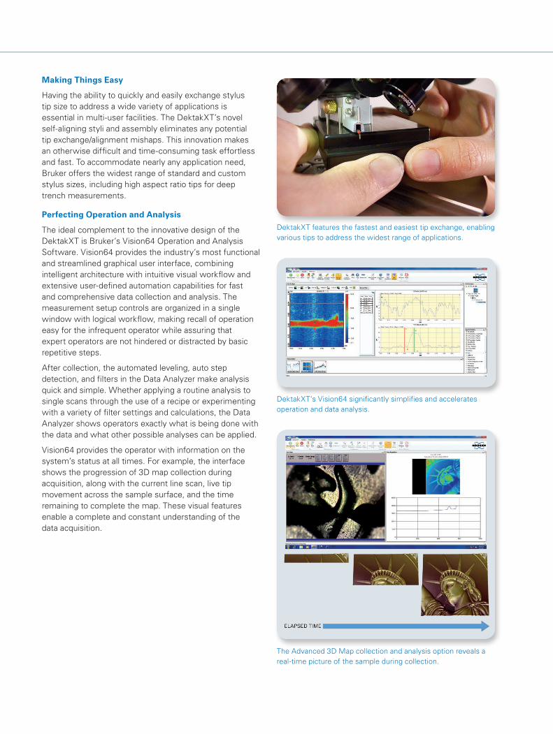
Having the ability to quickly and easily exchange stylus tip size to address a wide variety of applications is essential in multi-user facilities. The DektakXT’s novel self-aligning styli and assembly eliminates any potential tip exchange/alignment mishaps. This innovation makes an otherwise difficult and time-consuming task effortless and fast. To accommodate nearly any application need, Bruker offers the widest range of standard and custom stylus sizes, including high aspect ratio tips for deep trench measurements.
Perfecting Operation and Analysis
The ideal complement to the innovative design of the DektakXT is Bruker’s Vision64 Operation and Analysis Software. Vision64 provides the industry’s most functional and streamlined graphical user interface, combining intelligent architecture with intuitive visual workflow and extensive user-defined automation capabilities for fast and comprehensive data collection and analysis. The measurement setup controls are organized in a single window with logical workflow, making recall of operation easy for the infrequent operator while assuring that expert operators are not hindered or distracted by basic repetitive steps.
After collection, the automated leveling, auto step detection, and filters in the Data Analyzer make analysis quick and simple. Whether applying a routine analysis to single scans through the use of a recipe or experimenting with a variety of filter settings and calculations, the Data Analyzer shows operators exactly what is being done with the data and what other possible analyses can be applied.
Vision64 provides the operator with information on the system’s status at all times. For example, the interface shows the progression of 3D map collection during acquisition, along with the current line scan, live tip movement across the sample surface, and the time remaining to complete the map. These visual features enable a complete and constant understanding of the data acquisition.
DektakXT features the fastest and easiest tip exchange, enabling various tips to address the widest range of applications.
DektakXT‘s Vision64 significantly simplifies and accelerates operation and data analysis.
The Advanced 3D Map collection and analysis option reveals a real-time picture of the sample during collection.
Thin Film Inspection — Ensuring High Yield
Close monitoring of deposition and etch rate uniformity, as well as thin film stress, in semiconductor manufacturing can save valuable time and money. Non-uniformity of a film layer or too much stress, can result in poor yield and inferior end product performance. DektakXT provides the ability to quickly and easily set up and run automated multi-site measurement routines to verify the precise thickness of thin films across the wafer surface, down to the nanometer scale. The unmatched repeatability of the DektakXT gives engineers the accurate film thickness and stress measurements they need to precisely adjust etch and deposition processes to improve yields.
Surface Roughness Verification — Assuring Performance
The DektakXT is ideal for routine qualification of surface roughness on precision machined parts for a wide variety of industries, including automotive, aeropspace, and medical devices. For example, the roughness of the hydroxyapatite coating on the backside of an orthopedic implant influences its adhesive properties and efficacy once implanted. A quick analysis of the rough surface with a DektakXT confirms if the desired crystalline growth has been achieved and if the implant will pass production requirements. Using the Vision64 database with pass/fail criteria, quality assurance personnel can easily identify implants for rework or certify implant quality.
Critical Results for Multiple ApplicationsDektakXT
DektakXT 3D Map of hybrid circuit.
DektakXT can reliably measure thin films below 10nm.
This 2D trace shows the roughness from the backside of a knee implant.
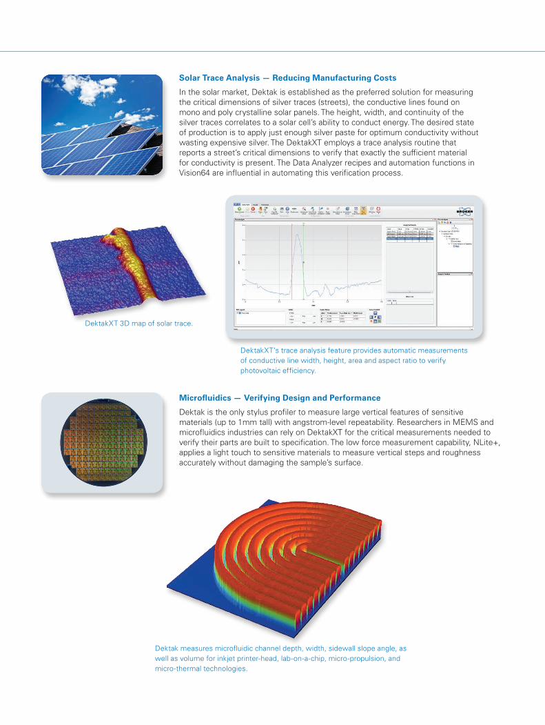
Solar Trace Analysis — Reducing Manufacturing Costs
In the solar market, Dektak is established as the preferred solution for measuring the critical dimensions of silver traces (streets), the conductive lines found on mono and poly crystalline solar panels. The height, width, and continuity of the silver traces correlates to a solar cell’s ability to conduct energy. The desired state of production is to apply just enough silver paste for optimum conductivity without wasting expensive silver. The DektakXT employs a trace analysis routine that reports a street’s critical dimensions to verify that exactly the sufficient material for conductivity is present. The Data Analyzer recipes and automation functions in Vision64 are influential in automating this verification process.
Microfluidics — Verifying Design and Performance
Dektak is the only stylus profiler to measure large vertical features of sensitive materials (up to 1mm tall) with angstrom-level repeatability. Researchers in MEMS and microfluidics industries can rely on DektakXT for the critical measurements needed to verify their parts are built to specification. The low force measurement capability, NLite+, applies a light touch to sensitive materials to measure vertical steps and roughness accurately without damaging the sample’s surface.
DektakXT 3D map of solar trace.
DektakXT‘s trace analysis feature provides automatic measurements of conductive line width, height, area and aspect ratio to verify photovoltaic efficiency.
Dektak measures microfluidic channel depth, width, sidewall slope angle, as well as volume for inkjet printer-head, lab-on-a-chip, micro-propulsion, and micro-thermal technologies.
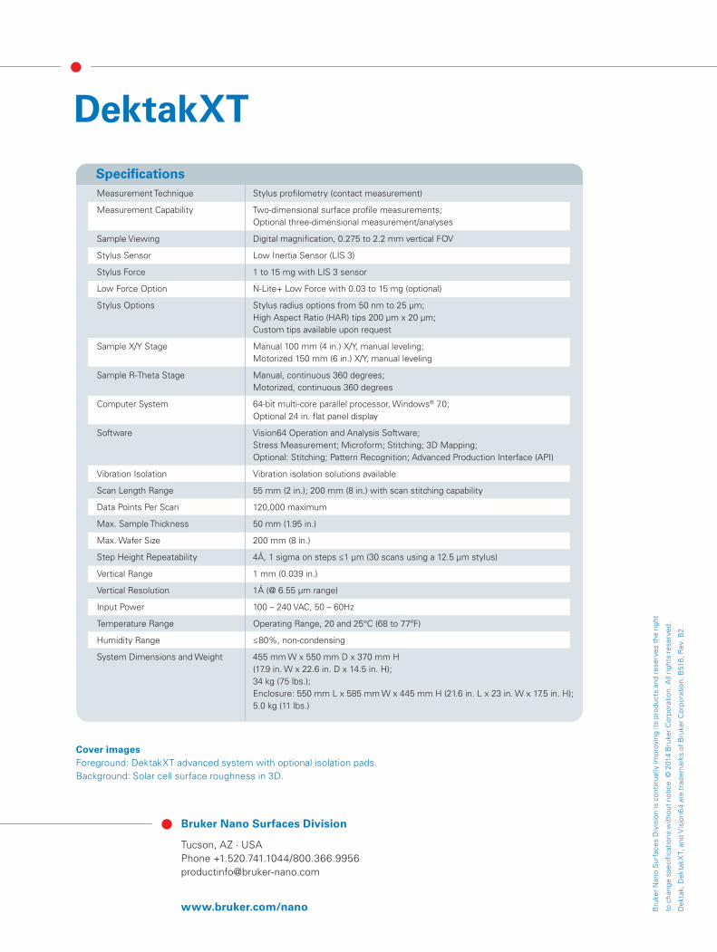
SpecificationsMeasurement Technique Stylus profilometry (contact measurement)
Measurement Capability Two-dimensional surface profile measurements; Optional three-dimensional measurement/analyses
Sample Viewing Digital magnification, 0.275 to 2.2 mm vertical FOV
Stylus Sensor Low Inertia Sensor (LIS 3)
Stylus Force 1 to 15 mg with LIS 3 sensor
Low Force Option N-Lite+ Low Force with 0.03 to 15 mg (optional)
Stylus Options Stylus radius options from 50 nm to 25 μm; High Aspect Ratio (HAR) tips 200 μm x 20 μm; Custom tips available upon request
Sample X/Y Stage Manual 100 mm (4 in.) X/Y, manual leveling; Motorized 150 mm (6 in.) X/Y, manual leveling
Sample R-Theta Stage Manual, continuous 360 degrees; Motorized, continuous 360 degrees
Computer System 64-bit multi-core parallel processor, Windows® 7.0; Optional 24 in. flat panel display
Software Vision64 Operation and Analysis Software; Stress Measurement; Microform; Stitching; 3D Mapping; Optional: Stitching; Pattern Recognition; Advanced Production Interface (API)
Vibration Isolation Vibration isolation solutions available
Scan Length Range 55 mm (2 in.); 200 mm (8 in.) with scan stitching capability
Data Points Per Scan 120,000 maximum
Max. Sample Thickness 50 mm (1.95 in.)
Max. Wafer Size 200 mm (8 in.)
Step Height Repeatability 4Å, 1 sigma on steps ≤1 μm (30 scans using a 12.5 μm stylus)
Vertical Range 1 mm (0.039 in.)
Vertical Resolution 1Å (@ 6.55 μm range)
Input Power 100 – 240 VAC, 50 – 60Hz
Temperature Range Operating Range, 20 and 25°C (68 to 77ºF)
Humidity Range ≤80%, non-condensing
System Dimensions and Weight 455 mm W x 550 mm D x 370 mm H (17.9 in. W x 22.6 in. D x 14.5 in. H); 34 kg (75 lbs.); Enclosure: 550 mm L x 585 mm W x 445 mm H (21.6 in. L x 23 in. W x 17.5 in. H); 5.0 kg (11 lbs.)
Bruker Nano Surfaces Division
Tucson, AZ · USAPhone +1.520.741.1044/[email protected]
www.bruker.com/nano Bru
ker
Nan
o S
urfa
ces
Div
isio
n is
con
tinua
lly im
prov
ing
its p
rodu
cts
and
rese
rves
the
rig
ht
to c
hang
e sp
ecifi
catio
ns w
ithou
t no
tice.
© 2
014
Bru
ker
Cor
pora
tion.
All
right
s re
serv
ed.
Dek
tak,
Dek
takX
T, a
nd V
isio
n64
are
trad
emar
ks o
f B
ruke
r C
orpo
ratio
n. B
516,
Rev
. B2
Cover imagesForeground: DektakXT advanced system with optional isolation pads.Background: Solar cell surface roughness in 3D.
DektakXT