Embed Size (px)
Citation preview
Project Training for suitable low cost PV technologies 316488–KESTCELLS DeliverableD3.3
1
Project no. 316488
Project Acronym: KESTCELLS
Project title: Training for suitable low cost PV technologies: development of kesterite based efficient
solar cells.
Industry-Academia Partnerships and Pathways
Start date of project: 01/09/2012
Duration: 48 months
Project coordinator: Dr. Edgardo Saucedo
Project coordinator organization name: IREC
Project website address: www.kestcells.eu
Deliverable 3.3
Kesterite-based solar cell with optimized buffer and window
layers and efficiency > 10%
Delivery date: Month 36 (July 2016)
Dissemination Level
PU Public
Document details:
Workpackage WP3: Implementation of solar cells
Partners EMPA / HZB
Authors Stefan G. Haass, Yaroslav E. Romanyuk, Ayodhya N. Tiwari
Document ID D3.3
Release Date --/--/2016
Project Training for suitable low cost PV technologies 316488–KESTCELLS DeliverableD3.3
2
Kesterite-based solar cell with optimized buffer and window
layers and efficiency > 10%
Introduction:
Overcoming the threshold of 10% conversion efficiency is challenging because of several issues
concerning the absorber layer synthesis:
Avoiding detrimental secondary phases like Zn(S,Se), CuSn(S,Se)3 and Cux(S,Se)
A well crystallized and dense morphology
Copper poor and zinc rich stoichiometry
Dealing with Sn loss during high temperature annealing
Stable and Ohmic back contact in the presence of Mo(S,Se)2 formation and kesterite phase
decomposition
This deliverable describes ways to overcome some of the above listed challenges and demonstrates
kesterite solar cells with more than 10% conversion efficiency. The CZTSSe absorbers are prepared
from precursors obtained from a solution approach with dimethyl sulfoxide (DMSO) as the solvent with
subsequent recrystallization by annealing under controlled atmosphere of selenium. Some commonly
reported problems of the DMSO-processed kesterite layers are their high porosity, non-uniformity, and
numerous grain boundaries that can lead to undesirable recombination. Here, we employ a three-stage
annealing process under controlled selenium atmosphere in an SiOx coated graphite box to drastically
improve the grain size and morphology of the absorber layer. Importantly, the Voc deficit can be reduced
to 0.57 V, which appears to be one of the lowest values reported for kesterite devices. Systematic
electrical characterization of absorbers and finished solar cells with time-resolved photoluminescence
(TRPL), temperature-dependent current–voltage measurements ( JV–T ), and admittance spectroscopy
(AS) are used to identify the reasons of the improved voltage. Additionally, a series with different
cadmium sulfide (CdS) layer thicknesses was processed in order to optimize the buffer layer.
Buffer layer:
Cadmium sulfide buffer layers still result in the highest device efficiencies, although alternative buffer
layers have been successfully applied to kesterite solar cells[2]. Therefore we optimized the CdS buffer
layer thickness by variation of the deposition time from 19 minutes to 26 minutes.
The CdS buffer layer thickness was measured by SEM cross sections and the finished devices were
characterized by current – voltage – measurements (J-V), external quantum efficiency (EQE) and time-
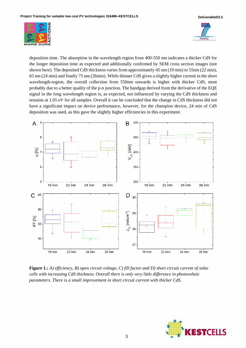
resolved photoluminescence (TRPL). Figure 1 shows the average efficiency, open circuit voltage (Voc),
short circuit current (JSC) and fill factor (FF) for all cells. The resulted efficiencies are very similar and
no trend is visible. The sample with 24 min deposition time yields a lower FF and therefore also a lower
efficiency. The Voc of all samples is very similar, however, the JSC shows a small increase with thicker
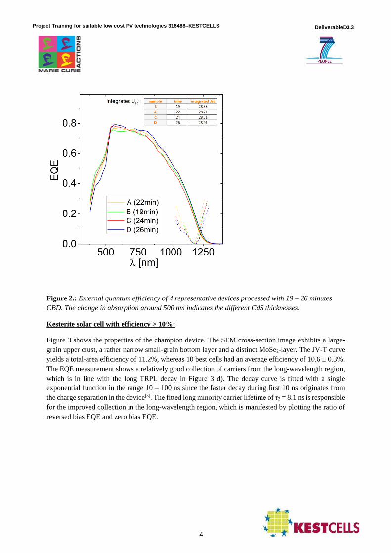
CdS. In Figure 2 the external quantum efficiency is shown for four representative cells for each
Project Training for suitable low cost PV technologies 316488–KESTCELLS DeliverableD3.3
3
deposition time. The absorption in the wavelength region from 400-550 nm indicates a thicker CdS for
the longer deposition time as expected and additionally confirmed by SEM cross section images (not
shown here). The deposited CdS thickness varies from approximately 45 nm (19 min) to 55nm (22 min),
65 nm (24 min) and finally 75 nm (26min). While thinner CdS gives a slightly higher current in the short
wavelength-region, the overall collection from 550nm onwards is higher with thicker CdS, most
probably due to a better quality of the p-n junction. The bandgap derived from the derivative of the EQE
signal in the long wavelength region is, as expected, not influenced by varying the CdS thickness and
remains at 1.05 eV for all samples. Overall it can be concluded that the change in CdS thickness did not
have a significant impact on device performance, however, for the champion device, 24 min of CdS
deposition was used, as this gave the slightly higher efficiencies in this experiment.
Figure 1.: A) efficiency, B) open circuit voltage, C) fill factor and D) short circuit current of solar
cells with increasing CdS thickness. Overall there is only very little difference in photovoltaic
parameters. There is a small improvement in short circuit current with thicker CdS.
Project Training for suitable low cost PV technologies 316488–KESTCELLS DeliverableD3.3
4
Figure 2.: External quantum efficiency of 4 representative devices processed with 19 – 26 minutes
CBD. The change in absorption around 500 nm indicates the different CdS thicknesses.
Kesterite solar cell with efficiency > 10%:
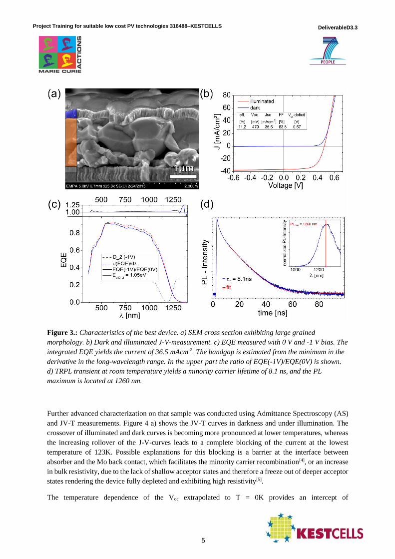
Figure 3 shows the properties of the champion device. The SEM cross-section image exhibits a large-
grain upper crust, a rather narrow small-grain bottom layer and a distinct MoSe2-layer. The JV-T curve
yields a total-area efficiency of 11.2%, whereas 10 best cells had an average efficiency of 10.6 ± 0.3%.
The EQE measurement shows a relatively good collection of carriers from the long-wavelength region,
which is in line with the long TRPL decay in Figure 3 d). The decay curve is fitted with a single
exponential function in the range 10 – 100 ns since the faster decay during first 10 ns originates from
the charge separation in the device[3]. The fitted long minority carrier lifetime of τ2 = 8.1 ns is responsible
for the improved collection in the long-wavelength region, which is manifested by plotting the ratio of
reversed bias EQE and zero bias EQE.
Project Training for suitable low cost PV technologies 316488–KESTCELLS DeliverableD3.3
5
Figure 3.: Characteristics of the best device. a) SEM cross section exhibiting large grained
morphology. b) Dark and illuminated J-V-measurement. c) EQE measured with 0 V and -1 V bias. The
integrated EQE yields the current of 36.5 mAcm-2. The bandgap is estimated from the minimum in the
derivative in the long-wavelength range. In the upper part the ratio of EQE(-1V)/EQE(0V) is shown.
d) TRPL transient at room temperature yields a minority carrier lifetime of 8.1 ns, and the PL
maximum is located at 1260 nm.
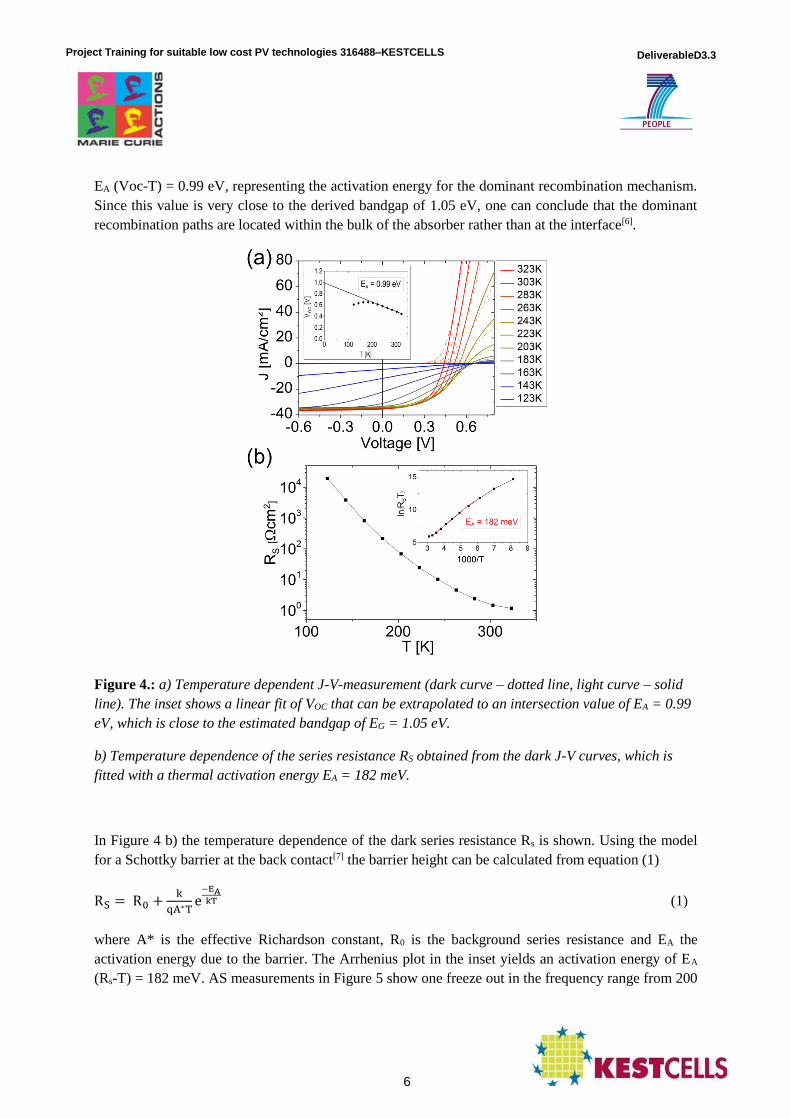
Further advanced characterization on that sample was conducted using Admittance Spectroscopy (AS)
and JV-T measurements. Figure 4 a) shows the JV-T curves in darkness and under illumination. The
crossover of illuminated and dark curves is becoming more pronounced at lower temperatures, whereas
the increasing rollover of the J-V-curves leads to a complete blocking of the current at the lowest
temperature of 123K. Possible explanations for this blocking is a barrier at the interface between
absorber and the Mo back contact, which facilitates the minority carrier recombination[4], or an increase
in bulk resistivity, due to the lack of shallow acceptor states and therefore a freeze out of deeper acceptor
states rendering the device fully depleted and exhibiting high resistivity[5].
The temperature dependence of the Voc extrapolated to T = 0K provides an intercept of
Project Training for suitable low cost PV technologies 316488–KESTCELLS DeliverableD3.3
6
EA (Voc-T) = 0.99 eV, representing the activation energy for the dominant recombination mechanism.
Since this value is very close to the derived bandgap of 1.05 eV, one can conclude that the dominant
recombination paths are located within the bulk of the absorber rather than at the interface[6].
Figure 4.: a) Temperature dependent J-V-measurement (dark curve – dotted line, light curve – solid
line). The inset shows a linear fit of VOC that can be extrapolated to an intersection value of EA = 0.99
eV, which is close to the estimated bandgap of EG = 1.05 eV.
b) Temperature dependence of the series resistance RS obtained from the dark J-V curves, which is
fitted with a thermal activation energy EA = 182 meV.
In Figure 4 b) the temperature dependence of the dark series resistance Rs is shown. Using the model
for a Schottky barrier at the back contact[7] the barrier height can be calculated from equation (1)
RS = R0 +k
qA∗Te
−EAkT (1)
where A* is the effective Richardson constant, R0 is the background series resistance and EA the
activation energy due to the barrier. The Arrhenius plot in the inset yields an activation energy of EA
(Rs-T) = 182 meV. AS measurements in Figure 5 show one freeze out in the frequency range from 200
Project Training for suitable low cost PV technologies 316488–KESTCELLS DeliverableD3.3
7
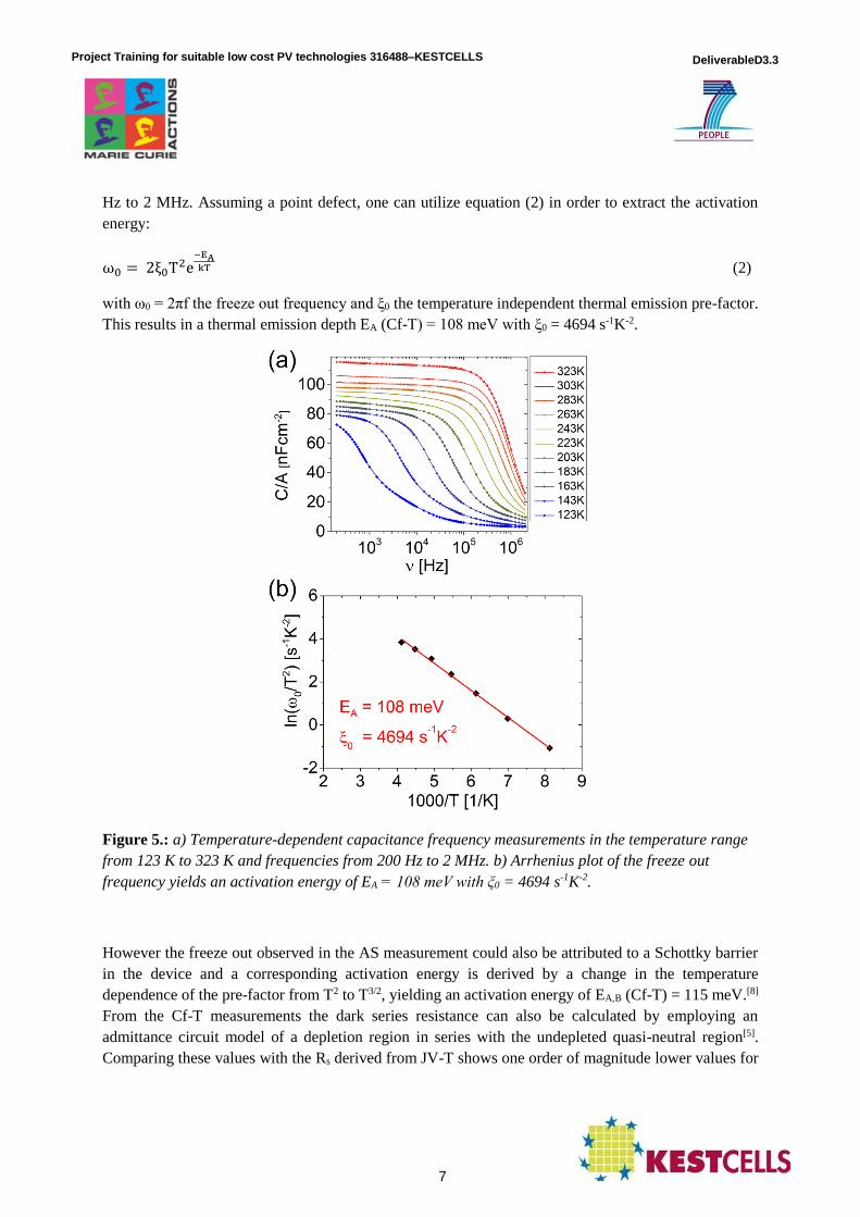
Hz to 2 MHz. Assuming a point defect, one can utilize equation (2) in order to extract the activation
energy:
ω0 = 2ξ0T2e−EA
kT (2)
with ω0 = 2πf the freeze out frequency and ξ0 the temperature independent thermal emission pre-factor.
This results in a thermal emission depth EA (Cf-T) = 108 meV with ξ0 = 4694 s-1K-2.
Figure 5.: a) Temperature-dependent capacitance frequency measurements in the temperature range
from 123 K to 323 K and frequencies from 200 Hz to 2 MHz. b) Arrhenius plot of the freeze out
frequency yields an activation energy of EA = 108 meV with ξ0 = 4694 s-1K-2.
However the freeze out observed in the AS measurement could also be attributed to a Schottky barrier
in the device and a corresponding activation energy is derived by a change in the temperature
dependence of the pre-factor from T2 to T3/2, yielding an activation energy of EA,B (Cf-T) = 115 meV.[8]
From the Cf-T measurements the dark series resistance can also be calculated by employing an
admittance circuit model of a depletion region in series with the undepleted quasi-neutral region[5].
Comparing these values with the Rs derived from JV-T shows one order of magnitude lower values for
Project Training for suitable low cost PV technologies 316488–KESTCELLS DeliverableD3.3
8
Rs obtained from AS, implying that the activation energies EA (Cf-T) and EA (Rs-T) are not attributed to
the same effect.
Conclusion:
In summary, an 11.2%-efficient (total cell area measurement) CZTSSe solar cell is fabricated using the
hydrazine-free DMSO solution approach. The best device features the Voc-deficit of only 0.57 V which
is amongst the lowest for solution processed CZTSSe devices. The open circuit voltage improvement
was possible because of the 3-stage annealing process in a silica-coated closed reactor, which enabled
an increased incorporation of selenium and large-grained microstructure. The reduced Voc-deficit is
attributed to an increased minority carrier lifetime, low diode saturation current and ideality factor,
which are signatures of the semiconductor material with a low concentration of recombination centers.
[1] S. Siebentritt, Thin Solid Films 2013, 535, 1.
[2] T. Ericson, J. J. Scragg, A. Hultqvist, J. T. Watjen, P. Szaniawski, T. Torndahl, C. Platzer-
Björkman, IEEE J. Photovolt. 2014, 4, 465.
[3] T. K. Todorov, J. Tang, S. Bag, O. Gunawan, T. Gokmen, Y. Zhu, D. B. Mitzi, Adv. Energy
Mater. 2013, 3, 34.
[4] R. Scheer, H.-W. Schock, Chalcogenide Photovoltaics: Physics, Technologies, and Thin Film
Devices, John Wiley & Sons, 2011.
[5] O. Gunawan, T. Gokmen, C. W. Warren, J. D. Cohen, T. K. Todorov, D. A. R. Barkhouse, S.
Bag, J. Tang, B. Shin, D. B. Mitzi, Appl. Phys. Lett. 2012, 100, 253905.
[6] V. Nadenau, U. Rau, A. Jasenek, H. W. Schock, J. Appl. Phys. 2000, 87, 584.
[7] O. Gunawan, T. K. Todorov, D. B. Mitzi, Appl. Phys. Lett. 2010, 97, 233506.
[8] T. Eisenbarth, T. Unold, R. Caballero, C. A. Kaufmann, H.-W. Schock, J. Appl. Phys. 2010,
107, 034509.