Embed Size (px)
Citation preview

1
DEMO MANUAL DC2703A-A-KIT
Rev. 0
DESCRIPTION
LT8491 High Voltage Buck-Boost Battery Charge Controller
with Maximum Power Point Tracking (MPPT) and I2C
The DC2703A-A-KIT contains the DC2703A (LT®8491 demo board) and DC1613A (USB-to-I2C controller). Together they provide a high performance buck-boost battery charger converter with an I2C interface. The LT8491 implements a maximum power point track-ing (MPPT) function and flexible charging profiles, suit-able for most battery types such as flooded and sealed lead acid batteries and Li-Ion batteries. A Microsoft Windows-Based GUI (Graphical User Interface) appli-cation called “simpleLT8491” is provided which can be downloaded here.
The DC2703A-A-KIT demo board is configured for 17V to 54V input voltage range and the power source can be a solar panel with 36 to 72 cells (up to 200W) or a DC voltage source. The LT8491 converter can operate from input voltages above, below or equal to the battery volt-age. Two input connectors are provided. An ideal diode controller LTC®4359 protects the DC power supply output from being back fed from the solar panel. This allows, for example, a 24VDC supply to be plugged in while a solar panel with higher voltage is being used to power the circuit. The DC2703A-A-KIT demo board output is set up for charging a 12V SLA battery with up to 16.6A charge current. The DC2703A-A-KIT demo board can be modified to support much higher output voltage, with modifications including higher voltage rating output side MOSFETs and capacitors.
The LT8491 includes a slave I2C compatible interface for digital control of the charger settings and digital readouts of charger telemetry and status. A Microsoft Windows-Based GUI (Graphical User Interface) application is pro-vided for this demo board, which makes it very easy to read charger telemetry and status data, as well as the All registered trademarks and trademarks are the property of their respective owners.
ability to change the charging algorithm by writing to the appropriate configuration registers. The LT8491 EEPROM on the DC2703A-A-KIT demo board is programmed with the onboard resistor values to accurately read charger telemetry and status registers data.
On-chip logic provides automatic true power point track-ing (MPPT) for solar powered applications. The MPPT function not only continuously tracks the maximum power point, but also periodically sweeps the input panel voltage in order to select the correct maximum on the power curve. In doing so, an increase in power harvested from the panel during partial shade conditions is possible when multiple peaks occur on the power curve. During periods of low light, a low power mode allows the char-ger to deliver a small charge current even if there is not enough light for the MPPT function to operate.
An RJ25 modular jack can be used to connect an exter-nal NTC temperature sensor mounted at the battery. This allows temperature compensation of the charge voltage, which is important for lead acid batteries. The same con-nector can be used for remote sensing of battery voltage, to compensate for voltage drops in long battery cables. The onboard LED displays the charge state.
The LT8491 data sheet gives a complete description of the device, operation and application information. The data sheet must be read in conjunction with this demo man-ual for DC2703A-A-KIT. The LT8491EUKJ is assembled in a 64-lead (7mm × 11mm) plastic QFN package with a thermal pad underneath the chip. Proper board layout is essential for maximum thermal performance.
Design files for this circuit board are available.

2
DEMO MANUAL DC2703A-A-KIT
Rev. 0
Figure 1. Efficiency vs Output Battery Charge Current (DC Input: VIN = 28V, VOUT = 14.2V)
Figure 2. Input and Output Currents vs Input Voltage (DC Input Current Limited to 10A, VOUT = 13.6V)
EFFICIENCY
DISSIPATION
CHARGE CURRENT (A)0 2 4 6 8 10 12 14 16 18
90
91
92
93
94
95
96
97
98
99
100
0
2
4
6
8
10
12
14
16
18
20
EFFI
CIEN
CY (%
)
DISSIPATION (W)
DC2703A-A-KIT F01
IOUT
IIN
INPUT VOLTAGE (V)10 15 20 25 30 35 40 45 50 55
0
2
4
6
8
10
12
14
16
18CU
RREN
T (A
)
DC2703A-A-KIT F02
SYMBOL PARAMETER CONDITIONS MIN TYP MAX UNITS
VIN Input Supply Range Note: Output Power Is Limited by Input Current Limit When VIN < 24V (See Figure 2)
17 30 54 V
VOUT Charge Voltage 14.2 V
IIN Maximum Input Current 10 A
IOUT Maximum Output Current VIN > 24V, VOUT = 12V 16.6 A
fSW Switching Frequency 150 kHz
POUT/PIN Efficiency at DC Input VIN = 48V, VOUT = 14.2V, IOUT = 15A VIN = 36V, VOUT = 14.2V, IOUT = 15A VIN = 24V, VOUT = 14.2V, IOUT = 8A
95.6 96.1 97.1
% % %
Note 1: VIN MIN and MAX specifications are for solar panel as an input power source. For further information refer to data sheet section: HW Config: Solar Panel Powered Charging. For DC supply as an input power source, VIN MIN can be as low as 10V.
TYPICAL PERFORMANCE CHARACTERISTICS
PERFORMANCE SUMMARY Specifications are at TA = 25°C
3
DEMO MANUAL DC2703A-A-KIT
Rev. 0
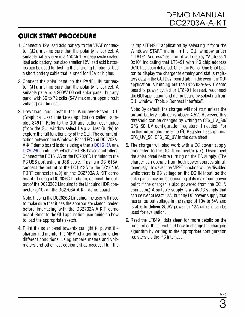
1. Connect a 12V lead acid battery to the VBAT connec-tor (J2), making sure that the polarity is correct. A suitable battery size is a 150Ah 12V deep cycle sealed lead acid battery, but also smaller 12V lead acid batter-ies can be used for testing the charging functions. Use a short battery cable that is rated for 15A or higher.
2. Connect the solar panel to the PANEL IN connec-tor (J1), making sure that the polarity is correct. A suitable panel is a 200W 60 cell solar panel, but any panel with 36 to 72 cells (54V maximum open circuit voltage) can be used.
3. Download and install the Windows-Based GUI (Graphical User Interface) application called “sim-pleLT8491”. Refer to the GUI application user guide (from the GUI window select Help > User Guide) to explore the full functionality of the GUI. The communi-cation between the Windows-Based PC and DC2703A-A-KIT demo board is done using either a DC1613A or a DC2026C Linduino®, which are USB-based controllers. Connect the DC1613A or the DC2026C Linduino to the PC USB port using a USB cable. If using a DC1613A, connect the output of the DC1613A to the DC1613A PORT connector (J9) on the DC2703A-A-KIT demo board. If using a DC2026C Linduino, connect the out-put of the DC2026C Linduino to the Linduino HDR con-nector (J10) on the DC2703A-A-KIT demo board.
Note: If using the DC2026C Linduino, the user will need to make sure that it has the appropriate sketch loaded before interfacing with the DC2703A-A-KIT demo board. Refer to the GUI application user guide on how to load the appropriate sketch.
4. Point the solar panel towards sunlight to power the charger and monitor the MPPT charger function under different conditions, using ampere meters and volt-meters and other test equipment as needed. Run the
“simpleLT8491” application by selecting it from the Windows START menu. In the GUI window under “LT8491 Address” section, it will display “Address 1 0x10” indicating that LT8491 with I2C chip address 0x10 has been detected. Click the Poll or One Shot but-ton to display the charger telemetry and status regis-ters data in the GUI Dashboard tab. In the event the GUI application is running but the DC2703A-A-KIT demo board is power cycled or LT8491 is reset, reconnect the GUI application and demo board by selecting from GUI window “Tools > Connect Interface”.
Note: By default, the charger will not start unless the output battery voltage is above 4.5V. However, this threshold can be changed by writing to CFG_UV_S0/CFG_S0_UV configuration registers if needed. For further information refer to I2C Register Descriptions: CFG_UV_S0, CFG_S0_UV in the data sheet.
5. The charger will also work with a DC power supply connected to the DC IN connector (J7). Disconnect the solar panel before turning on the DC supply. (The charger can operate from both power sources simul-taneously. However, the MPPT function will be disabled while there is DC voltage on the DC IN input, so the solar panel may not be operating at its maximum power point if the charger is also powered from the DC IN connector.) A suitable supply is a 24VDC supply that can deliver at least 12A, but any DC power supply that has an output voltage in the range of 10V to 54V and is able to deliver 250W power or 12A current can be used for evaluation.
6. Read the LT8491 data sheet for more details on the function of the circuit and how to change the charging algorithm by writing to the appropriate configuration registers via the I2C interface.
QUICK START PROCEDURE

4
DEMO MANUAL DC2703A-A-KIT
Rev. 0
Figure 3. SOLAR Panel and SLA Battery Connections
DC2703A-A-KIT F03
SOLAR PANEL
SLA BATTERY
+–
+
–
QUICK START PROCEDURE

5
DEMO MANUAL DC2703A-A-KIT
Rev. 0
Figure 4. DC2703A-A-KIT Connected to DC1613A and Windows-Based GUI “simpleLT8491” Application
QUICK START PROCEDURE

6
DEMO MANUAL DC2703A-A-KIT
Rev. 0
ITEM QTY REFERENCE PART DESCRIPTION MANUFACTURER/PART NUMBER
Required Circuit Components
1 4 C2, C6, C11, C12 CAP., 10μF, X7R, 100V, 20%, 2220, STACKED TDK, CKG57NX7R2A106M
2 1 C3 CAP., 150μF, ALUM.ELECT., 25V, 20%, 8mm × 10.5mm SMD SUN ELECTRONIC INDUSTRIES, 25HVH150M
3 2 C4, C8 CAP., 33μF, ALUM. ELECT., 63V, 20%, 10mm × 10.5mm SMD SUN ELECTRONIC INDUSTRIES, 63HVH33M
4 1 C13 CAP., 0.001μF, X7R, 100V, ±10%, 1206 WURTH ELEKTRONIK, 885012208106
5 1 C15 CAP., 1000pF, X7R, 16V, 10%, 0603 AVX, 0603YC102KAT2A
6 2 C16, C21 CAP., 0.01μF, X7R, 100V, 10%, 0603 WURTH ELEKTRONIK, 885012206114
7 2 C17, C18 CAP., 0.0033μF, X7R, 50V, 10%, 0603 WURTH ELEKTRONIK, 885012206086
8 2 C19, C20 CAP., 0.220μF, X7R, 16V, 10%, 0603 WURTH ELEKTRONIK, 885012206048
9 2 C22, C24 CAP., 0.470μF, X7R, 16V, 10%, 0603 WURTH ELEKTRONIK, 885012206050
10 1 C23 CAP., 2.2μF, X7R, 100V, 10%, 1210 AVX, 12101C225KAT2A
11 3 C26, C34, C37 CAP., 0.1μF, X7R, 16V, 10%, 0603 AVX, 0603YC104KAT2A
12 2 C27, C32 CAP., 1μF, X7R, 16V, 10%, 0603 WURTH ELEKTRONIK, 885012206052
13 1 C28 CAP., 1μF, X7R, 100V, 10%, 1210 AVX, 12101C105KAT2A
14 3 C29, C30, C31 CAP., 4.7μF, X5R, 16V, 20%, 0603 MURATA, GRM188R61C475MAAJD
15 2 C33, C35 CAP., 0.0047μF, X7R, 16V, 10%, 0603 WURTH ELEKTRONIK, 885012206038
16 1 C36 CAP., 220pF, C0G, 50V, 5%, 0603 AVX, 06035A221JAT2A
17 1 C38 CAP., 0.0068μF, X7R, 50V, 10%, 0603 WURTH ELEKTRONIK, 885012206088
18 1 C39 CAP., 0.068μF, X7R, 16V, 10%, 0603 WURTH ELEKTRONIK, 885012206045
19 2 D3, D4 DIODE, RECT., 200V, 1A, SOD-123F CENTRAL SEMI., CMMR1U-02 TR
20 2 D6, D7 DIODE, SCHOTTKY, 100V, 1A, POWERDI-123 DIODES INC., DFLS1100-7
21 1 L1 IND., 10μH, SHIELDED, HIGH CURRENT, 15%, 30A, 2.4mΩ WURTH ELEKTRONIK, 7443641000
22 2 M1, M6 XSTR., MOSFET, N-CH, 60V, PG-TDSON-8 INFINEON, BSC028N06NS
23 1 M2 XSTR., MOSFET, N-CH, 60V, 8-PIN PG-TDSON FL INFINEON, BSC016N06NSATMA1
24 2 M3, M4 XSTR., MOSFET, N-CHAN, 25V, PG-TDSON-8 INFINEON, BSC010NE2LSI
25 1 R1 RES., 5mΩ, 1%, 2W, 2512 TT ELECTRONICS, LRMAT2512-R005FT4
26 1 R2 RES., SENSE, 3mΩ, 1%, 2W, 2512 TT ELECTRONICS, LRMAT2512-R003FT4
27 1 R4 RES., 1.2Ω, 5%, 1/4W, 1206 VISHAY, CRCW12061R20JNEA
28 1 R5 RES., 30.1k, 1%, 1/10W, 0603 VISHAY, CRCW060330K1FKEA
29 1 R6 RES., 8.06k, 1%, 1/10W, 0603 YAGEO, RC0603FR-078K06L
30 4 R7, R9, R10, R47 RES., 1Ω, 1%, 1/10W, 0603 YAGEO, RC0603FR-071RL
31 7 R8, R11, R23, R29, R36, R44, R66
RES., 0Ω, 1/10W, 0603 BOURNS, CR0603-J/-000ELF
32 8 R12, R18, R21, R22, R26, R27, R41, R63
RES., 10Ω, 1%, 1/10W, 0603 VISHAY, CRCW060310R0FKEA
33 1 R13 RES., 3mΩ, 1%, 3W, 1225, METAL, SENSE SUSUMU, KRL6432E-M-R003-F-T1
34 6 R17, R49, R55, R58, R73, R74
RES., 4.99k, 1%, 1/10W, 0603 STACKPOLE, RMCF0603FT3R30
35 1 R20 RES., 3.3Ω, 1%, 1/10W, 0603 STACKPOLE, RMCF0603FT3R30
36 1 R30 RES., 196k, 1%, 1/10W, 0603 VISHAY, CRCW0603196KFKEA
37 1 R31 RES., 102k, 1%, 1/10W, 0603 VISHAY, CRCW0603102KFKEA
38 1 R37 RES., 5.9k, 1%, 1/10W, 0603 PANASONIC, ERJ3EKF5901V
39 2 R38, R65 RES., 53.6k, 1%, 1/10W, 0603 VISHAY, CRCW060353K6FKEA
PARTS LIST

7
DEMO MANUAL DC2703A-A-KIT
Rev. 0
ITEM QTY REFERENCE PART DESCRIPTION MANUFACTURER/PART NUMBER
40 3 R39, R56, R59 RES., 10k, 1%, 1/10W, 0603 VISHAY, CRCW060310K0FKEC
41 1 R40 RES., 3.48k, 1%, 1/10W, 0603 VISHAY, CRCW06033K48FKEA
42 1 R42 RES., 1.1k, 1%, 1/10W, 0603 PANASONIC, ERJ3EKF1101V
43 1 R43 RES., 11.3k, 1%, 1/10W, 0603 PANASONIC, ERJ3EKF1132V
44 1 R46 RES., 49.9k, 1%, 1/10W, 0603 NIC, NRC06F4992TRF
45 1 R51 RES., 18.2k, 1%, 1/10W, 0603 PANASONIC, ERJ3EKF1822
46 1 R52 RES., 21k, 1%, 1/10W, 0603 ROHM, MCR03EZPFX2102
47 1 R53 RES., 3.01k, 1%, 1/10W, 0603 VISHAY, CRCW06033K01FKEA
48 1 R57 RES., 301k, 1%, 1/10W, 0603 NIC, NRC06F3013TRF
49 1 R61 RES., 124k, 1%, 1/10W, 0603 PANASONIC, ERJ3EKF1243V
50 1 R64 RES., 110k, 1%, 1/10W, 0603 PANASONIC, ERJ3EKF1103V
51 1 R67 RES., 35.7k, 1%, 1/10W, 0603 NIC, NRC06F3572TRF
52 1 U1 IC., BATTERY CHARGE CONTROLLER ANALOG DEVICES, LT8491EUKJ#PBF
Additional Demo Board Circuit Components And Options
53 5 C1, C5, C7, C9, C10 CAP., OPTION, ALUM. ELECT., SMD OPT
54 1 C14 CAP., OPTION, 1206 OPT
55 1 C41 CAP., 1μF, X7R, 16V, 10%, 0603 WURTH ELEKTRONIK, 885012206052
56 1 D8 LED, OPTION, 0603 OPT: LUMEX OPTO/COMPONENTS INC., SML-LX0603SIW-TR
57 1 D9 LED, GREEN, COLORLESS DIFFUSED, 0603 OSRAM, LG L29K-G2J1-24-Z
58 1 F1 FUSE BLADE FAST ACTING, 30A, 58V, 10.9mm × 3.8mm × 8.8mm LITTLEFUSE, 0997030.WXN
59 1 FH1 FUSE HOLDER, 125V, 2-PIN, THT-HOLE LITTELFUSE, 178.6764.0001
60 1 HL1 IND., OPTION OPT
61 1 M5 XSTR., MOSFET, N-CHAN, 25V, PG-TDSON-8 OPT: INFINEON, BSC010NE2LSI
62 1 R24 RES., 0Ω, 1/10W, 0603 OPT: BOURNS, CR0603-J/-000ELF
63 1 R35 RES., OPTION, 0603 OPT
64 1 R45 RES., 1.3k, 1%, 1/10W, 0603 VISHAY, CRCW06031K30FKEA
65 2 R48, R62 RES., OPTION, 0603 OPT
66 1 R50 RES., 549Ω, 1%, 1/10W, 0603 VISHAY, CRCW0603549RFKEA
67 2 R68, R69 RES., 10k, 1%, 1/10W, 0603 VISHAY, CRCW060310K0FKEC
68 1 R75 RES., OPTION, 1206 OPT
69 1 R76 RES., 1Ω, 1%, 1/10W, 0603 OPT: YAGEO, RC0603FR-071RL
70 1 SW1 SWITCH, TACT., NO SPST, 0.05A, 12V, J-BEND, SMD 6.0mm × 3.5mm WURTH ELEKTRONIK, 434123050816
71 1 U4 IC., MEMORY, EEPROM, 2Kb (256×8), TSSOP-8 MICROCHIP, 24LC025-I/ST
Optional Remote Sense for VBAT: Installed
72 1 C25 CAP., 0.010μF, X7R, 16V, 10%, 0603 WURTH ELEKTRONIK, 885012206040
73 3 D1, D2, D10 DIODE, SWITCHING, 75V, 300mA, 350mW, SOT-23 DIODES INC., BAV99-7-F
74 1 D5 DIODE, OPTION, SOD-323 OPT
75 1 J3 CONN., RJ-25, FEMALE, 6-POS, 2.54mm, THT RA TE CONNECTIVITY, 5555165-1
76 1 Q2 XSTR., MOSFET, P-CH, 50V, 0.13A, SOT23-3 FAIRCHILD SEMI, BSS84
77 2 Q4, Q5 XSTR., NPN, 40V, 200mA, SOT23-3 ON SEMICONDUCTOR, MMBT3904LT1G
78 1 R14 RES., 100k, 1%, 1/10W, 0603 YAGEO, RC0603FR-07100KL
PARTS LIST

8
DEMO MANUAL DC2703A-A-KIT
Rev. 0
ITEM QTY REFERENCE PART DESCRIPTION MANUFACTURER/PART NUMBER
79 2 R15, R60 RES., 100Ω, 5%, 1W, 2512 PANASONIC, ERJ1TYJ101U
80 1 R19 RES., OPTION, 0603 OPT
81 1 R32 RES., 200k, 1%, 1/10W, 0603 NIC, NRC06F2003TRF
82 1 R33 RES., 27.4k, 1%, 1/10W, 0603 VISHAY, CRCW060327K4FKEA
83 1 R34 RES., 113k, 1%, 1/10W, 0603 PANASONIC, ERJ3EKF1133V
84 1 U2 IC., OP AMP, SO8 ANALOG DEVICES, LT1636CS8#PBF
Optional DC Input Source: Installed
85 1 C40 CAP., 2.2μF, X7R, 100V, 10%, 1210 AVX, 12101C225KAT2A
86 1 D11 DIODE, TVS, UNI-DIRECT, 70V, 400W, SMA DIODES INC., SMAT70A-13-F
87 1 D12 DIODE, ZENER, 12V, 150mW, SOD-523 DIODES INC., DDZ9699T-7
88 1 D13 DIODE, TVS, UNI-DIRECT, 24V, 400W, SMA DIODES INC., SMAJ24A-13-F
89 1 J7 ANDERSON PP15/45 1×2 ASSEMBLED FROM MP1-MP15 ANDERSON POWER, MULTI-PART PP15
90 1 M7 XSTR., MOSFET, N-CH, 100V, 80A, PG-TDSON-8 INFINEON, BSC070N10NS5
91 1 Q6 XSTR., NPN, 40V, 200mA, SOT23-3 ON SEMICONDUCTOR, MMBT3904LT1G
92 1 R70 RES., 100k, 1%, 1/10W, 0603 YAGEO, RC0603FR-07100KL
93 1 R71 RES., 33.2k, 1%, 1/10W, 0603 PANASONIC, ERJ3EKF3322V
94 1 R72 RES., 1k, 1%, 1/10W, 0603 VISHAY, CRCW06031K00FKEA
95 1 U3 IC., IDEAL DIODE CONTROLLER, 6-PIN DFN EP ANALOG DEVICES, LTC4359CDCB#PBF
Optional EXTVCC Disconnect: Not Installed
96 1 Q1 XSTR., MOSFET, P-CH, 50V, 0.13A, SOT23-3 OPT: FAIRCHILD SEMI, BSS84
97 1 Q3 XSTR., NPN, 40V, 200mA, SOT23-3 OPT: ON SEMICONDUCTOR, MMBT3904LT1G
98 1 R3 RES., 100k, 1%, 1/10W, 0603 OPT: YAGEO, RC0603FR-07100KL
99 1 R16 RES., 10Ω, 1%, 1/10W, 0603 OPT: VISHAY, CRCW060310R0FKEA
100 1 R25 RES., 200k, 1%, 1/10W, 0603 OPT: NIC, NRC06F2003TRF
101 1 R28 RES., 26.1k, 1%, 1/10W, 0603 OPT: NIC, NRC06F2612TRF
Hardware, Connectors, Etc.
102 2 J1, J2 ANDERSON PP15/45 1×2 ASSEMBLED FROM MP1-MP15 ANDERSON POWER, MULTI-PART PP15
103 2 J4, J6 CONN., HDR, MALE, 1×4, 2.54mm, STR, VERT, THT, AU HTSW SERIES SAMTEC, HTSW-104-07-G-S
104 1 J5 CONN., HEADER SHROUDED, M, 8-POS, 2.54mm, THT- HOLE STR WURTH ELEKTRONIK, 61200821621
105 2 J8, J12 CONN., HEADER, HDR, 8-POS, 2mm, ST THT-HOLE AMPHENOL, 98414-G06-08ULF
106 1 J9 CONN., HDR, SHROUDED, MALE, 2×6, 2mm, VERT, ST, THT AMPHENOL, 98414-G06-12ULF
107 1 J10 CONN., HDR, SHROUDED, MALE, 2×7, 2mm, VERT, ST, THT MOLEX, 87831-1420
108 1 J11 CONN., HDR, MALE, 1×4, 2.54mm, STR, VERT, THT, AU HTSW SERIES SAMTEC, HTSW-104-07-G-S
109 3 MP1, MP6, MP11 CONN., POWERPOLE, HOUSING, + PIN, RED, 15A, 1-POS ANDERSON POWER PRODUCTS, 1327
110 3 MP2, MP7, MP12 CONN., POWERPOLE, HOUSING, – PIN, BLACk, 15A, 1-POS ANDERSON POWER PRODUCTS, 1327G6
111 6 MP3, MP4, MP8, MP9, MP13, MP14
CONN., POWER, SKT, 25.7mm, RA/THT-HOLE ANDERSON POWER PRODUCTS, 1377G12-BK
112 3 MP5, MP10, MP15 CONN., PCB MTG STAPLES, 1×2, STR, 12mm × 14.5mm ANDERSON POWER PRODUCTS, 114555P2
113 4 MTG1, MTG2, MTG3, MTG4
SCREW, MACHINE, 4-40 × 3/4, PHILIPS PAN HEAD, STL, ZINC CR3 OLANDER CO, 4C25PPIZR
114 4 SO1, SO2, SO3, SO4 STANDOFF, F/F, HEX, 4-40 × 1-INCH KEYSTONE, 2205
115 13 TP1, TP2, TP3, TP4, TP6, TP7, TP8, TP9,
TP10, TP12, TP13, TP14, TP15 TEST POINT, SILVER PLATE, PHOSPHOR BRONZE, 3.81mm × 2.03mm, 2.29mm H, SMT
KEYSTONE, 5019
PARTS LIST

9
DEMO MANUAL DC2703A-A-KIT
Rev. 0
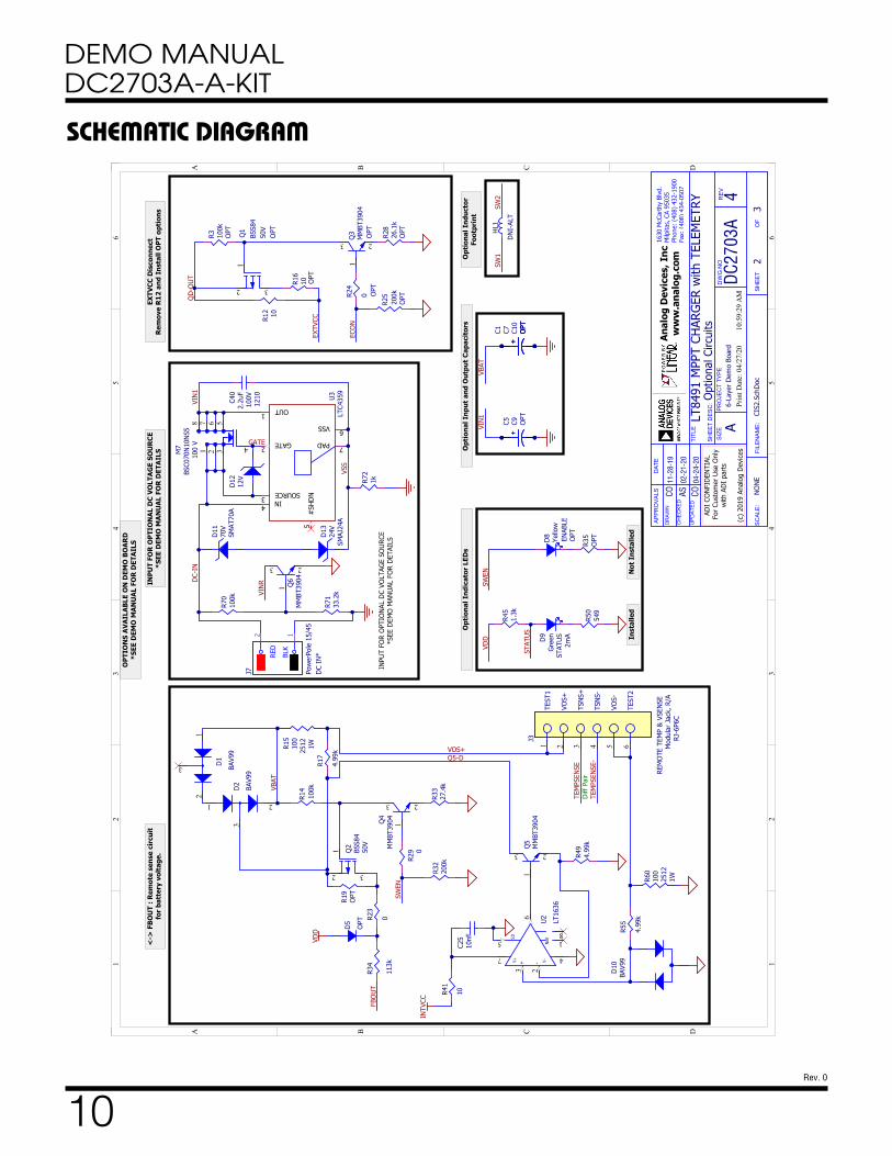
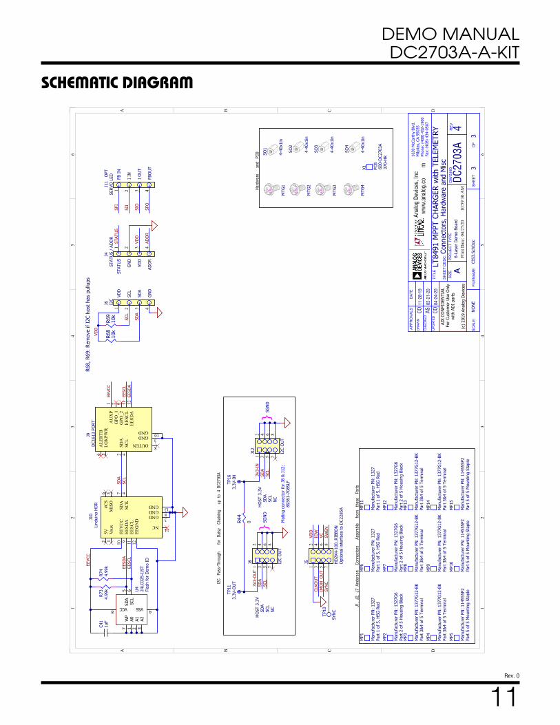
SCHEMATIC DIAGRAM
11
22
33
44
55
66
DD
CC
BB
AA
BG2
TG2
CSN
IMON
_IN
SW2
VIN
FBOU
T
CSP
BST2
SYNC
SS
SFI
SII
SIO
SFO
SDA
FBO
W
ADD
R
VDD
VDD
INTV
CC
INTV
CC
#SD
FBIN
CSN
IN
FBIW
ECO
N
INTV
CC
BG1
MO
DE
SW1
SW2
FBIR
RS+
RS+
TG1
SW1
VIN
R
EXTV
CC
SWE
N
SCL
VDD
VBA
T
VIN
R
CSNO
UT
CLKOUT
CKLDET
IOR
IOW
VIN
10k
R56
11.3
k
R43
1.1
k
R42
50V
NP0
220p
FC3
6
3.48
kR4
0
DFLS
1100
D7
2220
-J-X
210
0V
10u
F
C2
100n
FC3
7
1uF
C27
110k
R64
1225
3W3mR13
10uH
12
3
MTG
-NC
L1
25V
150u
F+
C3
21
CMM
R1U
-02
D3
10k
R59
470n
FC2
43.
3
R20
60V 4
5
3
678
12
BSC0
28N0
6N
SM
1
49.9
kR4
6
100
V12
10
2.2u
FC2
3
17V-
54V
PANE
LIN
*2 1
RED
BLK
J1
102k
R31
2512
2W3mR2
4.7n
FC3
5
8.06
kR6
2220
-J-X
210
0V
10u
FC1
2
0R36
10R63
DFLS
1100D6
1nF
C15
53.6
kR6
5LT84
91IN
TVC
C7
MODE 9
IMON
_IN
10
SHDN 11
CSN12
CSP13
LDO3
314
FBIN
15
FBOU
T16
IMON_OUT 17
RT 22
BG225
GATE
VCC
24BG123
BOOST227
TG228
SW229
SW131
TG132
BOOST133EX
TVCC
40
CSNO
UT41
CSPO
UT42
CSNI
N44
CSPI
N45
VIN
46
SYNC 21
VC 18
SS 19
CLKOUT 20
N/C 60
N/C 52
SRVO
_FB
OU
T38
SRVO
_FBI
N35
SRVO
_IIN
36
SRVO
_IOU
T37
SWE
N8
FBIR
1
ADD
R2
TEM
PSEN
SE3
VDD
4
FBO
W5
FBIW
6
STAT
US51
IOW 50
SWE
NO49
ECON
48
IIR
53
VIN
R54
GND 55
CLKDET 56
FBO
R57
GND 59
AVD
D58
SDA
61
GND 62
SCL
63
IOR 64
GND 65
U1
100
V12
06
1nF
C13
X5R
4.7u
FC3
0 X5R
4.7u
FC3
1
53.6
kR3
8
1R4
7
301kR5
7
35.7
kR6
7
1uF
C32
124k
R61
0R11
10R18
+C4
100n
FC3
4
1 OPT
R76
100
V
10n
FC2
150
V3.
3nF
C18
50V
3.3n
FC1
7
1R1
01R9
25V
4
5
3
678
12
BSC0
10NE
2LS
IM
3
4
5
3
678
12
OPT
M5
63V
33u
F
+
C8
100
V22
20-J
-X2
10u
FC1
1 X5R
4.7u
FC2
9
21k
R52
10R27
10R22
2512
2W5mR1
OPT
R48
100
V22
20-J
-X2
10u
FC6
50V
6.8n
FC3
8
SPST
-NO
SW1
100
V
10n
FC1
6
3.01
kR5
3
10k
R39
5.9
kR3
7
18.2
kR5
1
60V
4
5
3
678
12
BSC0
16N0
6N
SM
2
4.7n
FC3
3
10R26
60V
4
5
3
678
12
BSC0
28N0
6N
SM
6
196k
R30
470n
FC2
2
220n
FC2
0
0R8
10R21
25V
4
5
3
678
12
BSC0
10NE
2LS
IM
4
VBAT
*12
VSL
A
2 1
RED
BLK
J2
100
V12
10
1uF
C28
1206
1.2
R4
0R66
100n
FC2
6
30.1
k
R5
68n
FC3
9
4.99
kR5
8
220n
FC1
9
21
CMM
R1U
-02
D4
NOTE
S(U
NLES
SOT
HERW
ISE
SPEC
IFIE
D):
1-AL
LSM
DCA
PACI
TORS
ARE
0603
,16
V,X7
R2-
ALL
SMD
RESI
STOR
SAR
E06
03*-
See
Dem
oM
anua
lfo
rpr
oper
usag
ean
dw
arni
ngs
Rem
ove
R56
whe
nex
tern
alba
ttery
tem
pse
nsor
isus
ed
+ -
+ -
OPT
1206
C14
1R7
OPT
R62
OPT
1206
R75
Fuse
PN:
0997
030.
WXN
Fuse
:30
A/
58V
FH1
30A
58V
58V
30A
F1
Net Tie
Net Tie
Net Tie
Net Tie
Net
Tie
Net Tie
VBAT
-F
CSPI
N
TEM
PSEN
SE
Net
Tie
TEM
PSEN
SE-
QD-O
UT
QA-I
NVB
AT
TP1
GND
TP2
VIN
1TP
3
GND
TP4
VIN
RTP
5
GNDTP
8
SGN
D
TP9
ADD
RTP
6
TSN
S+TP
7
A
NON
ECI
S1.S
chD
oc
4
LT84
91 M
PPT
CHAR
GER
with
TEL
EMET
RY
6-La
yer
Dem
oBo
ard
13
DC27
03A
CO11
-28-
19
AS02
-21-
20
LT84
91 w
ith C
ore
Circ
uitry
04-2
4-20
CO
SIZE
SC
ALE
:
PR
OJE
CT
TYP
ED
WG
NO
REV
SH
EET
OF
FILE
NA
ME:
TITL
E
AP
PR
OVA
LSD
ATE
DR
AWN
CH
EC
KED
UP
DAT
ED
1630
McC
arth
yBl
vd.
Milp
itas,
CA95
035
Phon
e:(4
08)
432-
1900
Fax:
(408
)43
4-05
07
10:5
9:29
AM
04/2
7/20
Prin
t Dat
e:
ADI
CONF
IDE
NTIA
LFo
rCu
stom
erUs
eOn
lyw
ithAD
Ipa
rts
(c)
2019
Anal
ogDe
vic
es
SH
EET
DE
SC
:
Ana
log
Dev
ices
,In
cw
ww
.an
alog
.com
IMON
_IN
TP12
IMON
_OU
TTP
13
SGN
D
TP14
GNDTP
15
CSNI
N'
CSNOUT'VI
N
SW2
SW1
BST1
BST2
CSPO
UT
VC
STAT
US
CSPI
N
BST1
AVD
D
RT
->P
age
2:FB
OU
TR
emot
ese
nse
circ
uit
for
batt
ery
volt
age.
->P
age
2
->P
age
2->
Pag
e2
Snub
bers
-P
lace
atFE
Ts
Boo
stB
ias
-P
lace
atU
1
IMON
_OU
T
VIN
1
10
DEMO MANUAL DC2703A-A-KIT
Rev. 0
SCHEMATIC DIAGRAM
11
22
33
44
55
66
DD
CC
BB
AA
VIN
R
100V
1210
2.2u
FC4
0
100
VBS
C070
N10
NS5
4
53
621
78
M7
Pow
erPo
le 1
5/45
DC
IN*
2 1
RED
BLK
J7
70V
SMAT
70A
D11
LTC4
359
OUT1
GATE2
SOURCE3 IN4
#SH
DN
5
VSS 6
PAD 7
U3
24V
SMAJ
24A
D13
100k
R70
12V
D12
1
3 2
MM
BT39
04Q
6
33.2
kR7
1
1kR72
*SEE
DEM
O M
ANU
AL F
OR
DET
AILS
INPU
T FO
R O
PTIO
NAL
DC
VOLT
AGE
SOU
RCE
VIN
1
OPT
+C9
+C5
OPT
+C7 O
PT+
C1 OPT
+C1
0
VBAT
SWEN
OPT
R35Yello
w
OPT
ENAB
LE
D8
DC-
IN
Q6-
B
GATE
VSS
BAV9
9D
10VO
S-
TSN
S+
TEST
1
REM
OTE
TEM
P &
VSE
NSE
VOS+
TSN
S-
Mod
ular
Jac
k, R
/ARJ
-6P6
C
TEST
2
321 4 5 6
J3
100
2512
1WR6020
0kR3
2
10R41
0R2
9
MM
BT39
04 1
3 2
Q4
4.99
kR4
9
10nF
C25
1
3 2
MM
BT39
04Q
5
27.4
kR3
3
4.99
k
R55
<->
FB
OU
T :
Rem
ote
sens
e ci
rcui
tfo
r ba
tter
y vo
ltag
e.
Diff
Pai
rTE
MPS
ENSE
TEM
PSEN
SE-Q5-D
VOS+
100k
R14
0R23
100
2512 1WR1
5
OPT
D5
1
3
2
BAV9
9
D1
50V
1
32
BSS8
4Q
21
3
2
BAV9
9
D2
4.99
k
R17
113k
R34
OPT
R19
VDD
VBAT
FBO
UT
0 OPT
R24
10R12
OPT
MM
BT39
041
3 2Q3OPT
BSS8
4
1
32
50V
Q1
OPT
100k
R3
OPT
10R16
OPT
26.1
kR2
8
EXTV
CC
QD
-OU
T
ECO
N
EXTV
CC
Dis
conn
ect
Rem
ove
R12
and
Ins
tall
OP
T op
tion
s
OPT
200k
R25
DN
I-AL
T
HL1
SW2
SW1Opt
ion
al I
ndu
ctor
Foot
prin
t
STAT
US
VDD
549
R50
1.3k
R45
Gre
enST
ATU
S2m
AD9
Q2-
G
SWEN
A
NO
NE
CIS2
.Sch
Doc
4
LT84
91 M
PPT
CHAR
GER
with
TEL
EMET
RY
6-La
yer
Dem
o Bo
ard
23
DC27
03A
CO11
-28-
19
AS02
-21-
20
Opt
iona
l Circ
uits
04-2
4-20
CO
SIZE
SCAL
E:
PRO
JEC
TTY
PED
WG
NO
REV
SHEE
TO
FFI
LEN
AME:
TITL
E
APPR
OVA
LSD
ATE
DR
AWN
CH
ECKE
D
UPD
ATED
1630
McC
arth
y Bl
vd.
Milp
itas,
CA
9503
5Ph
one:
(40
8) 4
32-1
900
Fax:
(40
8) 4
34-0
507
10:5
9:29
AM
04/2
7/20
Prin
tDat
e:
ADI
CON
FID
ENTI
ALFo
r Cu
stom
er U
se O
nly
with
AD
I pa
rts
(c)
2019
Ana
log
Dev
ices
SHEE
T D
ESC
:
Ana
log
Dev
ices
,Inc
ww
w.a
nalo
g.co
m
INTV
CC
INP
UT
FOR
OP
TIO
NA
L D
C V
OLT
AG
E SO
UR
CE
*SEE
DEM
O M
AN
UA
L FO
R D
ETA
ILS O
ptio
nal I
nput
and
Out
put
Cap
acit
ors
Opt
iona
l Ind
icat
or L
EDs
Inst
alle
dN
ot I
nsta
lled
VIN
1
OP
TIO
NS
AV
AIL
AB
LE O
N D
EMO
BO
AR
D*S
EE D
EMO
MA
NU
AL
FOR
DET
AIL
S
-+V+ V-Nu
llSD 1
23
5
6
8
7 4
LT16
36
U2
11
DEMO MANUAL DC2703A-A-KIT
Rev. 0
SCHEMATIC DIAGRAM
11
22
33
44
55
66
DD
CC
BB
AA
VDD
IOW
CLKO
UT
VCIM
ON
_OU
TSW
ENSY
NCSD
ASC
L
VDD
SDA
SCL
SDA
SCL
10k
R68
Lind
uino
HD
R
SDA
7
EESD
A9
Vaux
15V
2#C
S6
SCK
4EE
VC
C10
MIS
O5
EESC
L11
EEG
ND
12
NC 14
GND 13
GND 3
GND 8
J10
4.99
kR7
44.
99k
R73
SCL
I2C
VDD
SDA
GN
D
21 3 4
J6
I2C
OU
T
HO
ST3.
3VSD
ASC
LN
C
SGN
D
8936
1-70
8SLF
12
34
56
78
J8
24LC
025-
I/ST
SDA
5
VCC8
A01
A12
A23
VSS 4
WP
7
SCL
6 U4
Flas
hfo
rD
emo
ID
10k
R69
R68,
R69
: Re
mov
e if
I2C
host
has
pul
lups
}
DC1
613
PORT G
PO_1
7
GPO
_29
AU
XP
1
SDA
2
ALE
RTB
6
SCL
4
GND 10
LGK
PWR
5
EESC
L11
EESD
A12
GND 3OUTEN 8
J9
EESD
AEE
SDA
EESC
LEE
SCL
EEVC
C
EEVC
C
HD
2X4-
100_
RIBB
ON
Opt
iona
lint
erfa
ceto
DC2
285A
12
34
56
78
J5
1uF
C41
4-40
MTG
1
4-40
MTG
2
4-40
MTG
3
4-40
MTG
4
SO1
4-40
x1in
SO2
4-40
x1in
SO3
4-40
x1in
SO4
4-40
x1in
SYN
C
TP10
Man
ufac
ture
rPN
:13
27Pa
rt1
of5,
HSG
Red
MP1
Man
ufac
ture
rPN
:13
27G
6Pa
rt2
of5
Hou
sing
Blac
k
MP2
Man
ufac
ture
rPN
:13
77G
12-B
KPa
rt3&
4of
5Te
rmin
al
MP3
Man
ufac
ture
rPN
:13
77G
12-B
KPa
rt3&
4of
5Te
rmin
al
MP4
Man
ufac
ture
rPN
:11
4555
P2Pa
rt5
of5
Mou
ntin
gSt
aple
MP5
J1,
J2,
J7An
ders
onCo
nnec
tors
Asse
mbl
efro
mth
ese
Parts
Man
ufac
ture
rPN
:13
27Pa
rt1
of5,
HSG
Red
MP6
Man
ufac
ture
rPN
:13
27G
6Pa
rt2
of5
Hou
sing
Blac
k
MP7
Man
ufac
ture
rPN
:13
77G
12-B
KPa
rt3&
4of
5Te
rmin
al
MP8
Man
ufac
ture
rPN
:13
77G
12-B
KPa
rt3&
4of
5Te
rmin
al
MP9
Man
ufac
ture
rPN
:11
4555
P2Pa
rt5
of5
Mou
ntin
gSt
aple
MP1
0
Man
ufac
ture
rPN
:13
27Pa
rt1
of5,
HSG
Red
MP1
1
Man
ufac
ture
rPN
:13
27G
6Pa
rt2
of5
Hou
sing
Blac
k
MP1
2
Man
ufac
ture
rPN
:13
77G
12-B
KPa
rt3&
4of
5Te
rmin
al
MP1
3
Man
ufac
ture
rPN
:13
77G
12-B
KPa
rt3&
4of
5Te
rmin
al
MP1
4
Man
ufac
ture
rPN
:11
4555
P2Pa
rt5
of5
Mou
ntin
gSt
aple
MP1
5
3.3V
-OU
TTP
11
SFI
SII
SIO
SFO
STAT
US
VDD
ADD
RAD
DR
GN
D
STAT
US
/AD
DR
STAT
US
VDD
21 3 4
J4
IO
UT
FBIN
OPT
SERV
OLE
D
IIN
FBO
UT
21 3 4
J11
SDA
SCL
I2C
OU
T
HO
ST3.
3VSD
ASC
LN
C
SGN
D
12
34
56
78
J12
}
3.3V
-IN
TP16
0R44
600-
DC2
703A
370-
HR
X1 PCB
3V3-
OU
T3V
3-IN
Hard
war
ean
dPC
B
A
NO
NE
CIS3
.Sch
Doc
4
LT84
91 M
PPT
CHAR
GER
with
TEL
EMET
RY
6-La
yer
Dem
oBo
ard
33
DC27
03A
CO11
-28-
19
AS02
-21-
20
Conn
ecto
rs,H
ardw
are
and
Mis
c04
-24-
20CO
SIZE
SCAL
E:
PRO
JEC
TTY
PED
WG
NO
REV
SHEE
TO
FFI
LEN
AME:
TITL
E
APPR
OVA
LSD
ATE
DR
AWN
CH
ECKE
D
UPD
ATED
1630
McC
arth
yBl
vd.
Milp
itas,
CA95
035
Phon
e:(4
08)
432-
1900
Fax:
(408
)43
4-05
07
10:5
9:30
AM
04/2
7/20
Prin
t Dat
e:
ADI
CON
FID
ENTI
ALFo
rCu
stom
erU
seO
nly
with
ADI
part
s
(c)
2019
Anal
ogD
evic
es
SHEE
T D
ESC
:
Anal
og D
evic
es, I
ncw
ww
.ana
log.
com
I2C
Pass
-Thr
ough
for
Dais
yCh
aini
ngup
to4
DC27
03A
Mat
ing
conn
ecto
rfo
rJ8
&J1
2:

12
DEMO MANUAL DC2703A-A-KIT
Rev. 0
Figure 5. DC2703A-A-KIT Top Side
BOARD PHOTO: TOP SIDE

13
DEMO MANUAL DC2703A-A-KIT
Rev. 0
Figure 6. DC2703A-A-KIT Bottom Side
Information furnished by Analog Devices is believed to be accurate and reliable. However, no responsibility is assumed by Analog Devices for its use, nor for any infringements of patents or other rights of third parties that may result from its use. Specifications subject to change without notice. No license is granted by implication or otherwise under any patent or patent rights of Analog Devices.
BOARD PHOTO: BOTTOM SIDE

14
DEMO MANUAL DC2703A-A-KIT
Rev. 0
ANALOG DEVICES, INC. 2020
07/20www.analog.com
ESD Caution ESD (electrostatic discharge) sensitive device. Charged devices and circuit boards can discharge without detection. Although this product features patented or proprietary protection circuitry, damage may occur on devices subjected to high energy ESD. Therefore, proper ESD precautions should be taken to avoid performance degradation or loss of functionality.
Legal Terms and Conditions By using the evaluation board discussed herein (together with any tools, components documentation or support materials, the “Evaluation Board”), you are agreeing to be bound by the terms and conditions set forth below (“Agreement”) unless you have purchased the Evaluation Board, in which case the Analog Devices Standard Terms and Conditions of Sale shall govern. Do not use the Evaluation Board until you have read and agreed to the Agreement. Your use of the Evaluation Board shall signify your acceptance of the Agreement. This Agreement is made by and between you (“Customer”) and Analog Devices, Inc. (“ADI”), with its principal place of business at One Technology Way, Norwood, MA 02062, USA. Subject to the terms and conditions of the Agreement, ADI hereby grants to Customer a free, limited, personal, temporary, non-exclusive, non-sublicensable, non-transferable license to use the Evaluation Board FOR EVALUATION PURPOSES ONLY. Customer understands and agrees that the Evaluation Board is provided for the sole and exclusive purpose referenced above, and agrees not to use the Evaluation Board for any other purpose. Furthermore, the license granted is expressly made subject to the following additional limitations: Customer shall not (i) rent, lease, display, sell, transfer, assign, sublicense, or distribute the Evaluation Board; and (ii) permit any Third Party to access the Evaluation Board. As used herein, the term “Third Party” includes any entity other than ADI, Customer, their employees, affiliates and in-house consultants. The Evaluation Board is NOT sold to Customer; all rights not expressly granted herein, including ownership of the Evaluation Board, are reserved by ADI. CONFIDENTIALITY. This Agreement and the Evaluation Board shall all be considered the confidential and proprietary information of ADI. Customer may not disclose or transfer any portion of the Evaluation Board to any other party for any reason. Upon discontinuation of use of the Evaluation Board or termination of this Agreement, Customer agrees to promptly return the Evaluation Board to ADI. ADDITIONAL RESTRICTIONS. Customer may not disassemble, decompile or reverse engineer chips on the Evaluation Board. Customer shall inform ADI of any occurred damages or any modifications or alterations it makes to the Evaluation Board, including but not limited to soldering or any other activity that affects the material content of the Evaluation Board. Modifications to the Evaluation Board must comply with applicable law, including but not limited to the RoHS Directive. TERMINATION. ADI may terminate this Agreement at any time upon giving written notice to Customer. Customer agrees to return to ADI the Evaluation Board at that time. LIMITATION OF LIABILITY. THE EVALUATION BOARD PROVIDED HEREUNDER IS PROVIDED “AS IS” AND ADI MAKES NO WARRANTIES OR REPRESENTATIONS OF ANY KIND WITH RESPECT TO IT. ADI SPECIFICALLY DISCLAIMS ANY REPRESENTATIONS, ENDORSEMENTS, GUARANTEES, OR WARRANTIES, EXPRESS OR IMPLIED, RELATED TO THE EVALUATION BOARD INCLUDING, BUT NOT LIMITED TO, THE IMPLIED WARRANTY OF MERCHANTABILITY, TITLE, FITNESS FOR A PARTICULAR PURPOSE OR NONINFRINGEMENT OF INTELLECTUAL PROPERTY RIGHTS. IN NO EVENT WILL ADI AND ITS LICENSORS BE LIABLE FOR ANY INCIDENTAL, SPECIAL, INDIRECT, OR CONSEQUENTIAL DAMAGES RESULTING FROM CUSTOMER’S POSSESSION OR USE OF THE EVALUATION BOARD, INCLUDING BUT NOT LIMITED TO LOST PROFITS, DELAY COSTS, LABOR COSTS OR LOSS OF GOODWILL. ADI’S TOTAL LIABILITY FROM ANY AND ALL CAUSES SHALL BE LIMITED TO THE AMOUNT OF ONE HUNDRED US DOLLARS ($100.00). EXPORT. Customer agrees that it will not directly or indirectly export the Evaluation Board to another country, and that it will comply with all applicable United States federal laws and regulations relating to exports. GOVERNING LAW. This Agreement shall be governed by and construed in accordance with the substantive laws of the Commonwealth of Massachusetts (excluding conflict of law rules). Any legal action regarding this Agreement will be heard in the state or federal courts having jurisdiction in Suffolk County, Massachusetts, and Customer hereby submits to the personal jurisdiction and venue of such courts. The United Nations Convention on Contracts for the International Sale of Goods shall not apply to this Agreement and is expressly disclaimed.