Embed Size (px)
Citation preview
1dc996f
DEMO MANUAL DC996
DESCRIPTION
LTC2208/LTC2208-14/LTC2217/LTC2216/LTC2215
16-Bit/14-Bit 80Msps to130Msps ADCs
Demonstration circuit 996 supports a family of 16-/14-bit 80Msps to 130Msps ADCs. Each assembly features one of the following devices: LTC®2208, LTC2208-14, LTC2217, LTC2216, LTC2215 high speed, high dynamic range ADCs.
This demonstration circuit only supports LVDS operation. For demonstration of CMOS output signaling, please see DC854.
Other members of this family include the LTC2207, a 105Msps 16-bit CMOS-only version of this device, as well as lower speed versions and single-ended clock ver-sions. These 7mm × 7mm QFN devices are supported by Demonstration Circuits 918 and 919 (for single-ended clock input).
L, LT, LTC, LTM, Linear Technology and the Linear logo are registered trademarks and PScope is a trademark of Linear Technology Corporation. All other trademarks are the property of their respective owners.
Several versions of the 996 demo board supporting the LTC2208 16-bit, LTC2217 16-bit and LTC2208-14 14-bit series of A/D converters are listed in Table 1. Depending on the required resolution, sample rate and input frequency, the DC996 is supplied with the appropriate ADC and with an optimized input circuit. The circuitry on the analog inputs is optimized for analog input frequencies below 70MHz or from 70MHz to 140MHz. For higher input frequencies, contact the factory for support.
Design files for this circuit board are available at http://www.linear.com/demo
Table 1. DC996 VariantsDC996 VARIANTS ADC PART NUMBER RESOLUTION MAXIMUM SAMPLE RATE INPUT FREQUENCY
996B-A LTC2208 16-Bit 130Msps 1MHz to 70MHz
996B-B LTC2208 16-Bit 130Msps 70MHz to 140MHz
996B-C LTC2208-14 14-Bit 130Msps 1MHz to 70MHz
996B-D LTC2208-14 14-Bit 130Msps 70MHz to 140MHz
996B-E LTC2217 16-Bit 105Msps 1MHz to 70MHz
996B-F LTC2217 16-Bit 105Msps 70MHz to 140MHz
996B-G LTC2216 16-Bit 80Msps 1MHz to 70MHz
996B-H LTC2216 16-Bit 80Msps 70MHz to 140MHz
996B-I LTC2215 16-Bit 65Msps 1MHz to 70MHz
996B-J LTC2215 16-Bit 65Msps 70MHz to 140MHz
996A-P LTC2208 16-Bit 130Msps >140MHz
996A-Q LTC2208-14 14-Bit 130Msps >140MHz

2dc996f
DEMO MANUAL DC996
QUICK START PROCEDURE
PERFORMANCE SUMMARY (TA = 25°C)
PARAMETER CONDITION VALUE
Supply Voltage Depending On Sampling Rate and the A/D Converter Provided, This Supply Must Provide Up To 700mA.
Optimized for 3.3V [3.15V⇔3.45V Min/Max]
Analog Input Range Depending on PGA Pin Voltage 1.5VP-P to 2.25VP-P
Logic Input Voltages Minimum Logic HighMaximum Logic Low
2V0.8V
Logic Output Voltages (Differential) Nominal Logic Levels (100Ω Load)Minimum Logic levels (100Ω Load)
350mV/2.1V Common Mode247mV/2.1V Common Mode
Sampling Frequency (Convert Clock Frequency) See Table 1
Convert Clock Level 50Ω Source Impedance, AC-Coupled or Ground Referenced (Convert Clock Input Is Capacitor Coupled On Board and Terminated with 50Ω.)
2VP-P⇔2.5VP-P Sine Wave or Square wave
Resolution See Table 1
Input frequency range See Table 1
SFDR See Applicable Data Sheet
SNR See Applicable Data Sheet
Demonstration circuit 996 is easy to set up to evaluate the performance of the LTC2208/LTC2208-14/LTC2217 A/D converters. Refer to Figure 1 for proper measurement equipment setup and follow this procedure:
Setup
If a DC890 QuikEval™ II Data Acquisition and Collection System was supplied with the DC996 demonstration circuit, follow the DC890 Quick Start Guide to install the required software and for connecting the DC890 to the DC996 and to a PC.
DC996 Demonstration Circuit Board Jumpers
The DC996 demonstration circuit board should have the following jumper settings as default: (as per Figure 1).
Figure 1 shows DC996A, the DC996B is shown in Figure 7.
J2: Mode (VCC) 2's Complement CDS Off
J3: SHDN: (Run) Dither (Off)
J4: Rand (Off) PGA 1x
J9: Unused power connector
Applying Power and Signals to the DC996 Demonstration Circuit
Apply 3.3V across the pins marked “+3.3V” and “PWR GND” on the DC996. The DC996 demonstration circuit requires up to 700mA depending on the sampling rate and the A/D converter supplied. If a DC890 is used to acquire data from the DC996, the DC890 must be provided with an external 6V ±0.5V 1A supply on turrets G7(+) and G1(–) or the adjacent 2.1mm power jack to support the power requirements of the Xilinx Spartan 3 FPGA active terminations used to terminate the LVDS repeaters on the DC996. The DC890 will not activate the LVDS mode unless the DC890 detects external power present.
If external power is not present the DC890 will not config-ure the FPGA for LVDS terminations as this would result in exceeding the USB 500mA limit. The DC890 contains an onboard electronic circuit breaker which will shut off the DC890 if external power is removed while the FPGA is configured for LVDS active terminations.

3dc996f
DEMO MANUAL DC996
QUICK START PROCEDURE
Figure 1. DC996A Setup (Zoom for Detail). See Figure 7 for DC996B
Encode Clock
Note: This is not a logic-compatible input. It is terminated with 50Ω. Apply an encode clock to the SMA connector on the DC996 demonstration circuit board marked “J7 ENCODE INPUT”. This is a transformer-coupled input, terminated on the secondary side in two steps, 100Ω at the transformer with final termination at the ADC at 100Ω.
For the best noise performance, the ENCODE INPUT must be driven with a very low jitter source. When using a sinusoidal generator, the amplitude should often be as large as possible, up to 3VP-P or 13dBm. Using bandpass filters on the clock and the analog input will improve the
noise performance by reducing the wideband noise power of the signals. Data sheet FFT plots are taken with 10-pole LC filters made by TTE (Los Angeles, CA) to suppress signal generator harmonics, non-harmonically related spurs and broad band noise. Low phase noise Agilent 8644B generators are used with TTE bandpass filters for both the clock input and the analog input.
Apply the analog input signal of interest to the SMA con-nectors on the DC996 demonstration circuit board marked “J5 ANALOG INPUT”. These inputs are capacitive coupled to Balun transformers ETC1-1-13, or directly coupled through flux-coupled transformers ETC1-1T.

4dc996f
DEMO MANUAL DC996
An internally generated conversion clock output is avail-able on J1 which could be collected via a logic analyzer, or other data collection system if populated with a SAMTEC MEC8-150 type connector or collected by the DC890 Data Acquisition Board using the PScope™ System Software provided or downloaded from the Linear Technology website at http://www.linear.com/designtools/software/. If a DC890 was provided, follow the DC890 Quick Start Guide and the instructions below.
To start the data collection software if “PScope.exe”, is installed (by default) in \Program Files\LTC\PScope\, double click the PScope Icon or bring up the run window under the start menu and browse to the PScope directory and select PScope.
If the DC996 demonstration circuit is properly connected to the DC890, PScope should automatically detect the DC996, and configure itself accordingly. If necessary the procedure below explains how to manually configure PScope.
Under the Configure menu, go to ADC Configuration. Check the Config Manually box and use the following configuration options:
• 16-Bit (or 14-Bit if using LTC2208-14)
• Alignment: Left-16
• Bipolar (2’s complement)
• Positive clock edge
• Type: LVDS
If everything is hooked up properly, powered and a suit-able convert clock is present, clicking the “Collect” button should result in time and frequency plots displayed in the PScope window. Additional information and help for PScope is available in the DC890 Quick Start Guide and in the online help available within the PScope program itself.
QUICK START PROCEDURE
Analog Input Network
For optimal distortion and noise performance the RC network on the analog inputs should be optimized for the analog input frequencies of interest. At this point in time, the circuit in Figure 3 for input frequencies below 70MHz. For input frequencies from 70MHz to 140MHz, the circuit in Figure 2 is used. These two input networks cover a broad bandwidth and are not optimized for operation at a specific input frequency.
For higher frequencies, a single balun (ETC1-1-13) is populated on a DC996A board.
In almost all cases, filters will be required on both analog input and encode clock to provide data sheet SNR.
The filters should be located close to the inputs to avoid reflections from impedance discontinuities at the driven end of a long transmission line. Most filters do not present 50Ω outside the passband.
The DC996A board has provision for a bandpass filter prior to the balun. This may be populated if the board is customized for a given frequency band. (Figure 5)
In some cases, 3dB to 10dB pads may be required to obtain low distortion.
If your generator cannot deliver full-scale signals without distortion, you may benefit from a medium power ampli-fier based on a Gallium Arsenide Gain block prior to the final filter. This is particularly true at higher frequencies where operational amplifiers may be unable to deliver the combination of low noise figure and high IP3 point required. A high order filter can be used prior to this final amplifier, and a relatively lower Q filter used between the amplifier and the demo circuit.
For advice on drive circuits or for input frequencies greater than 220MHz, or for higher order bandpass filtering prior to the ADC, contact the factory for support.

5dc996f
DEMO MANUAL DC996
QUICK START PROCEDURE
0.1μF
AIN+
AIN–
2.2μF
VCM
LTC2208ANALOGINPUT
0.1μF
0.1μF5Ω
33Ω
33Ω 5Ω
10Ω
49.9Ω
10Ω
T11:1
RESISTORS, CAPACITORSARE 0402 PACKAGE SIZEEXCEPT 2.2μF
T1MA/COM ETC1-1-13
T2COILCRAFT WBC1-1L70MHz TO 200MHz
Figure 2. Analog Front-End Circuit For 70MHz+
Figure 3. Analog Front-End Circuit For 1MHz < AIN < 70MHz
0.1μF
AIN+
AIN–
2.2μF
8.2μF
VCM
LTC2208ANALOGINPUT
0.1μF
0.1μF5Ω
33Ω
33Ω 5Ω
10Ω
49.9Ω
10Ω
T11:1
RESISTORS, CAPACITORSARE 0402 PACKAGE SIZEEXCEPT 2.2μF
T1MA/COM ETC1-1-13
T2COILCRAFT WBC1-1L1MHz TO 70MHz
For input frequencies less than 5MHz, or greater than 150MHz, other input networks may be more appropriate. Please consult the factory for suggestions on drivers and networks if your signal sources extend outside these ranges, or if you experience difficulties driving these sug-gested networks.
As this board has a black solder mask, in order to improve the thermal performance, Figure 4 is a picture of the top side in colors that are easier to digest. The dielectric under the input network (bluish pads) is 20 mils, otherwise, dielectric thickness is 6 mils.
This board is used only for 200MHz+ applications. The input network of Figure 5 is devised to be populated with a bandpass filter.
Gerber or PDF files of this board are available.
If the higher frequency board is ordered without requesting a bandpass filter, C6 is a counterpart to C7, providing a DC block, C23 is a 0Ω resistor.
If this is populated as a BP filter, The reactance of L1 and L3, and the series of C6 and C5 (and C21 and C23) should be between 50Ω and 33Ω. The reactance of L2 should match that of 1/2 C6^+C5.
The ratio of C5 to C6 will determine coupling be-tween the two resonators, with a high ratio giving a narrow pass band.
As an example, for center frequency of 260MHz; –3dB BW of 150MHz, C6, C23 = 27pF; C5, C21 = 68pF; L1, L3 = 18 nH; L2 = 7.5nH.
This has a flat passband over 80MHz. See Figure 6.
This filter is not intended as a band-defining filter, but simply to minimize noise BW prior to the ADC, and to minimize 2nd and 3rd originating in a drive amplifier. 2nd harmonic of 260 is down at 1.

6dc996f
DEMO MANUAL DC996
QUICK START PROCEDURE
Figure 4. DC996A Artwork
Figure 5. Input Filter for DC996A Board

7dc996f
DEMO MANUAL DC996
QUICK START PROCEDURE
Figure 8. DC996B Artwork
Figure 6. Input Filter Frequency Response for DC996A BoardFigure 7. DC996B Board—Two Transformer Version

8dc996f
DEMO MANUAL DC996
PARTS LIST
ITEM QTY REFERENCE PART DESCRIPTION MANUFACTURER/PART NUMBERDC996A General BOM
1 0 C4 (Option) CAP~NPO~1.8pF~50V~0.25pF~0402 AVX, 04025A1R8CAT2A2 1 C8 CAP~NPO~1.8pF~50V~0.25pF~0402 AVX, 04025A1R8CAT2A3 1 C12 CAP~X5R~0.01μF~16V~10%~0402 AVX, 0402YC103KAT4 15 C15-16, C20, C22, C25-32, C34-36 CAP~X5R~0.1μF~10V~10%~0402 AVX, 0402ZD104KAT5 0 C10, C11 (Option)6 6 C1-3, C6, C7, C23 CAP~X7R~0.01μF~16V~10%~0603 AVX, 0603YC103KAT7 2 C18, C19 CAP~X7R~0.1μF~16V~10%~0603 AVX, 0603YC104KAT8 0 C21 (Option) 9 2 C13, C17 CAP~X5R~2.2μF~10V~20%~0805 AVX, 0805ZD225MAT
10 3 C14, C24, C38 CAP~X5R~4.7μF~10V~20%~0805 AVX, 0805ZD475MAT11 0 C5 (Option) 12 4 J2, J3, J4, J9 HEADER~3X2~2mm COMM_CON/2202S-06G213 2 J5, J7 CONN~SMA 50Ω EDGE-LAUNCH E.F. Johnson, 142-0701-85114 0 L1 (Option)15 1 L2 RES~0Ω_JUMPER~0603 AAC, CJ06-000M16 0 L3 (Option)17 19 R13, R16-23, R30-35, R38-41 RES~100Ω~5%~1/20~0201 VISHAY, CRCW0201100RJNED18 1 R15 RES~100Ω~1%~1/16~0402 VISHAY, CRCW0402100RFKED19 1 R24 RES~100k~1%~1/16~0402 VISHAY, CRCW0402100KFKED20 2 R11-12 RES~33.2Ω~1%~1/16~0402 VISHAY, CRCW040233R2FKED21 2 R1, R2 RES~49.9Ω~1%~1/16~0402 VISHAY, CRCW040249R9FKEA22 6 R4, R5, R9, R10, R27, R28 RES~4.99Ω~1%~1/16W~0402 VISHAY, CRCW04024R99FKED23 3 R25, R26, R29 RES~4990Ω~1%~1/16~0402 VISHAY, CRCW04024K99FKED24 0 R3 (Option)25 2 R14, R37 RES~100Ω~1%~1/16W~0603 VISHAY, CRCW0603100RFKEA26 3 R6-8 RES~1000Ω~1%~1/16W~0603 VISHAY, CRCW06031K00FKEB27 2 R42, R43 FERRITE BEAD~SMT~1206 MURATA, BLM31PG330SN1L28 2 T1, T2 XFRM~RF~SMT~1:1 BALUN MACOM, MABA-007159-00000029 1 U1 (Bal to 1298A) IC~SERIAL_EEPROM~TSSOP8 MICROCHIP, 24LC025-I /ST30 2 U3, U4 BUFFER~LVDS~OCTAL FAIRCHILD, FIN1108MTDX31 1 U5 BUFFER~LVDS~SINGLE FAIRCHILD, FIN1101K8X32 4 TP1, TP2, TP4, TP5 TURRET MILL MAX, 2308-02-00-80-00-00-07-0033 4 Z (STAND-OFF) STAND-OFF, NYLON 0.25'" tall KEYSTONE, 8831(SNAP ON)34 5 SHUNT, 0.079" Center SAMTEC, 2SN-BK-G35 2 STENCIL, 20X20 STENCIL 996A, 20X20
DC996A-P1 1 U2 (DC996A-P) IC~ADC~130Msps~16-BIT~QFN-64 LINEAR_TECH/LTC2208CUP#PBF2 1 FAB, PRINTED CIRCUIT BOARD DEMO CIRCUIT #996A
DC996A-Q1 1 U2 (DC996A-Q) IC~ADC~130Msps~14-BIT~QFN-64 LINEAR_TECH/LTC2208CUP-14#PBF2 1 FAB, PRINTED CIRCUIT BOARD DEMO CIRCUIT #996A

9dc996f
DEMO MANUAL DC996
PARTS LIST
ITEM QTY REFERENCE PART DESCRIPTION MANUFACTURER/PART NUMBERDC996B General BOM
1 5 C1-C3, C6-7 CAP~X7R~0.01μF~16V~10%~0603 AVX/0603YC103KAT2 2 C13, C17 CAP~X5R~2.2μF~10V~20%~0805 AVX/0805ZD225MAT3 3 C14, C24, C38 CAP~X5R~4.7μF~10V~20%~0805 AVX/0805ZD475MAT4 15 C15-16, C20, C22, C25-C32, C34-C36 CAP~X5R~0.1μF~10V~10%~0402 AVX/0402ZD104KAT5 0 C18, C19(Option) CAP~X7R~0.1μF~16V~10%~0603 AVX/0603YC104KAT6 1 C4 (Also C9-C10 options) CAP~NPO~8.2pF~50V~0.25pF~0402 AVX/04025A8R2CAT2A7 2 C5, C12 CAP~X5R~0.01μF~16V~10%~0402 AVX/0402YC103KAT8 3 J2-4 HEADER~3 × 2~2mm COMM_CON/2202S-06G29 0 J9 (Option) HEADER~3 × 2~2mm COMM_CON/2202S-06G210 2 J5, J7 CONN~SMA 50Ω EDGE-LAUNCH AMPHENOL_CONNEX/13235711 2 R42-R43 FERRITE BEAD~SMT~1206 MURATA/BLM31PG330SN1L12 2 R9-R10 RES~10Ω~1%~1/16~0402 AAC/CR05-10R0FM13 1 R15 RES~100Ω~1%~1/16~0402 AAC/CR05-1000FM14 1 R37 RES~100Ω~1%~1/16W~0603 AAC/CR16-1000FM15 19 R13, R16-R23, R30-R35, R38-R41 RES~100Ω~5%~1/20~0201 ACC/CR20-101JM16 3 R6-8, R14 RES~1k~1%~1/16W~0603 AAC/CR16-1001FM17 1 R24 RES~100k~1%~1/16~0402 AAC/CR05-1003FM18 2 R1-R2 RES~49.9Ω~1%~1/16~0402 AAC/CR05-49R9FM19 0 R3 (OPTION) RES~100Ω~1%~1/16W~0603 AAC/CR16-1000FM20 2 R11-R12 RES~33.2Ω~1%~1/16~0402 AAC/CR05-33R2FM21 3 R25, R26, R29 RES~4990Ω~1%~1/16~0402 AAC/CR05-4991FM22 2 R27-R28 RES~10Ω~5%~1/20~0201 PANASONIC, ERJ-1GEJ100C23 2 R4-R5 RES~5.1Ω~1%~1/16~0402 AAC/CR05-5R1FM24 1 T3 XFRM~RF~SMT~1:1 BALUN M/A-COM, ETC1-1-13 (Leaded)
M/A-COM, MABA-007159-000000 (PbF)25 4 TP1-2, TP4-5 TURRET MILL_MAX/2308-226 1 U1 IC~Serial_EEPROM~TSSOP8 MICROCHIP/24LC025-I /ST27 2 U3, U4 BUFFER~LVDS~OCTAL FAIRCHILD/FIN1108MTD28 1 U5 BUFFER~LVDS~SINGLE FAIRCHILD/FIN1101K8X29 4 Z (STAND-OFF) STAND-OFF, NYLON 0.25" tall KEYSTONE, 8831(SNAP ON)30 5 SHUNT, 0.079" Center SAMTEC, 2SN-BK-G31 2 STENCIL, 20 × 20 STENCIL 996B, 20X20
DC996B-A1 1 C8 CAP~NPO~4.7pF~50V~0.25pF~0402 AVX/04025A4R7CAT2A2 2 C9-C10 CAVP~NPO~8.2pF~50V~0.25pF~0402 AVX/04025A8R2CAT2A3 1 L1 IND~56nH~5%~0603 MURATA/LQP18MN56NG02D4 2 R36, R44 RES~86.6~1%~1/16W~0603 AAC/CR16-86R6FM5 1 R45 RES~86.6~1%~1/16~0402 AAC/CR05-86R6FM6 1 T1 BALUN~RF~SMT~1:1 M/A-COM, ETC1-1-13 (Leaded)
M/A-COM, MABA-007159-000000 (PbF)7 1 T2 XFRM~RF~SMT~1:1CT M/A-COM, ETC1-1T (Leaded)
M/A-COM, MABAES0060 (PbF)8 1 U2 (D/C 0619) ADC~16BIT~130MSPS (Lot# T23920.2) LINEAR/LTC2208IUP#PBF 9 1 FAB, PRINTED CIRCUIT BOARD DEMO CIRCUIT 996B-A

10dc996f
DEMO MANUAL DC996
DC966B-E1 1 C8 CAP~NPO~4.7pF~50V~0.25pF 0402 AVX, 04025A4R7CAT2A2 2 C9-10 CAP~NPO~8.2pF~50V~0.25pF 0402 AVX, 04025A8R2CAT2A3 1 L1 IND~56nH~5% 0603 MURATA, LQP18MN56NG02D4 2 R36, R44 RES~86.6Ω~1%~1/16W 0603 VISHAY, CRCW060386R6FKEA5 1 R45 RES~86.6Ω~1%~1/16 0402 VISHAY, CRCW040286R6FKED6 1 T1 BALUN~RF~SMT~1:1 M/A-COM, MABA-007159-000000 (PbF)7 1 T2 XFRM~RF~SMT~1:1CT M/A-COM, MABAES0060 (PbF)8 1 U2 ADC~16-BIT~105Msps LINEAR, LTC2217IUP#PBF 9 1 FAB, PRINTED CIRCUIT BOARD DEMO CIRCUIT 996B
PARTS LIST
ITEM QTY REFERENCE PART DESCRIPTION MANUFACTURER/PART NUMBERDC996B-B
1 1 C8 CAP~NPO~1.8pF~50V~0.25pF~0402 AVX/04025A1R8CAT2A2 2 C9-C10 CAP~NPO~3.9pF~50V~0.25pF~0402 AVX/04025A3R9CAT2A3 1 L1 IND~18nH~5%~0603 MURATA/LQP18MN18NG02D4 2 R36, R44 RES~43.2Ω~1%~1/16W~0603 AAC/CR16-43R2FM5 1 R45 RES~182Ω_JUMPER~0402 AAC/CR05-1820FM6 1 T1 BALUN~RF~SMT~1:1 M/A-COM, ETC1-1-13 (Leaded) M/A-COM,
MABA-007159-000000 (PbF)7 1 T2 TRANSFORMER, WBC1-1L COILCRAFT, WBC1-1L8 1 U2 D/C 0619 ADC~16-BIT~130Msps, Lot# T23920.2 LINEAR/LTC2208IUP#PBF9 1 FAB, PRINTED CIRCUIT BOARD DEMO CIRCUIT #996B-B
DC996B-C1 1 C8 CAP~NPO~4.7pF~50V~0.25pF~0402 AVX/04025A4R7CAT2A2 2 C9-C10 CAP~NPO~8.2pF~50V~0.25pF~0402 AVX/04025A8R2CAT2A3 1 L1 IND~56nH~5%~0603 MURATA/LQP18MN56NG02D4 2 R36, R44 RES~86.6Ω~1%~1/16W~0603 AAC/CR16-86R6FM5 1 R45 RES~86.6Ω~1%~1/16~0402 AAC/CR05-86R6FM6 1 T1 BALUN~RF~SMT~1:1 M/A-COM, ETC1-1-13 (Leaded)
M/A-COM, MABA-007159-000000 (PbF)7 1 T2 XFRM~RF~SMT~1:1CT M/A-COM, ETC1-1T (Leaded)
M/A-COM, MABAES0060 (PbF)8 1 U2 (Lot #T23307.1) ADC~14BIT~130MSPS (D/C 0604) LINEAR/LTC2208IUP-14#PBF9 1 FAB, PRINTED CIRCUIT BOARD DEMO CIRCUIT #996B-C
DC996B-D1 1 C8 CAP~NPO~1.8pF~50V~0.25pF~0402 AVX/04025A1R8CAT2A2 2 C9-C10 CAP~NPO~3.9pF~50V~0.25pF~0402 AVX/04025A3R9CAT2A3 1 L1 IND~18nH~5%~0603 MURATA/LQP18MN18NG02D4 2 R36, R44 RES~43.2Ω~1%~1/16W~0603 AAC/CR16-43R2FM5 1 R45 RES~182Ω_JUMPER~0402 AAC/CR05-1820FM6 1 T1 BALUN~RF~SMT~1:1 M/A-COM, ETC1-1-13 (Leaded)
M/A-COM, MABA-007159-000000 (PbF)7 1 T2 TRANSFORMER, WBC1-1L Coilcraft, WBC1-1L8 1 U2 (Lot #T23307.1) ADC~14-BIT~130Msps (D/C 0604) LINEAR/LTC2208IUP-14#PBF9 1 FAB, PRINTED CIRCUIT BOARD DEMO CIRCUIT #996B-D

11dc996f
DEMO MANUAL DC996
ITEM QTY REFERENCE PART DESCRIPTION MANUFACTURER/PART NUMBERDC966B-F
1 1 C8 CAP~NPO~1.8pF~50V~0.25pF 0402 AVX, 04025A1R8CAT2A2 2 C9-10 CAP~NPO~3.9pF~50V~0.25pF 0402 AVX, 04025A3R9CAT2A 3 1 L1 IND~18nH~5% 0603 MURATA, LQP18MN18NG02D 4 2 R36, R44 RES~43.2Ω~1%~1/16W 0603 VISHAY, CRCW060343R2FKEA 5 1 R45 RES~182Ω_JUMPER 0402 VISHAY, CRCW0402182RFKED 6 1 T1 BALUN~RF~SMT~1:1 M/A-COM, MABA-007159-000000 (PbF)7 1 T2 TRANSFORMER, WBC1-1TL Coilcraft, WBC1-1TLC8 1 U2 ADC~16-BIT~105Msps, LINEAR, LTC2217IUP#PBF9 1 FAB, PRINTED CIRCUIT BOARD DEMO CIRCUIT #996B
DC966B-G1 1 C8 CAP~NPO~4.7pF~50V~0.25pF 0402 AVX, 04025A4R7CAT2A2 2 C9-10 CAP~NPO~8.2pF~50V~0.25pF 0402 AVX, 04025A8R2CAT2A3 1 L1 IND~56nH~5% 0603 MURATA, LQP18MN56NG02D4 2 R36, R44 RES~86.6Ω~1%~1/16W 0603 VISHAY, CRCW060386R6FKEA5 1 R45 RES~86.6Ω~1%~1/16 0402 VISHAY, CRCW040286R6FKED6 1 T1 BALUN~RF~SMT~1:1 M/A-COM, MABA-007159-000000 (PbF)7 1 T2 XFRM~RF~SMT~1:1CT M/A-COM, MABAES0060 (PbF)8 1 U2 ADC~16-BIT~80Msps LINEAR, LTC2216IUP#PBF 9 1 FAB, PRINTED CIRCUIT BOARD DEMO CIRCUIT 996B
DC966B-H1 1 C8 CAP~NPO~1.8pF~50V~0.25pF 0402 AVX, 04025A1R8CAT2A2 2 C9-10 CAP~NPO~3.9pF~50V~0.25pF 0402 AVX, 04025A3R9CAT2A 3 1 L1 IND~18nH~5% 0603 MURATA, LQP18MN18NG02D 4 2 R36, R44 RES~43.2Ω~1%~1/16W 0603 VISHAY, CRCW060343R2FKEA 5 1 R45 RES~182Ω_JUMPER 0402 VISHAY, CRCW0402182RFKED 6 1 T1 BALUN~RF~SMT~1:1 M/A-COM, MABA-007159-000000 (PbF)7 1 T2 TRANSFORMER, WBC1-1TL Coilcraft, WBC1-1TLC8 1 U2 ADC~16-BIT~80Msps, LINEAR, LTC2216IUP#PBF9 1 FAB, PRINTED CIRCUIT BOARD DEMO CIRCUIT #996B
DC966B-I1 1 C8 CAP~NPO~4.7pF~50V~0.25pF 0402 AVX, 04025A4R7CAT2A2 2 C9-10 CAP~NPO~8.2pF~50V~0.25pF 0402 AVX, 04025A8R2CAT2A3 1 L1 IND~56nH~5% 0603 MURATA, LQP18MN56NG02D4 2 R36, R44 RES~86.6Ω~1%~1/16W 0603 VISHAY, CRCW060386R6FKEA6 1 T1 (Bal to 1098A-F) BALUN~RF~SMT~1:1 M/A-COM, MABA-007159-000000 (PbF)7 1 T2 (Bal to 1098A-C) XFRM~RF~SMT~1:1CT M/A-COM, MABAES0060 (PbF)8 1 U2 ADC~16-BIT~65Msps LINEAR, LTC2215IUP#PBF 9 1 FAB, PRINTED CIRCUIT BOARD DEMO CIRCUIT 996B
DC966B-J1 1 C8 CAP~NPO~1.8pF~50V~0.25pF 0402 AVX, 04025A1R8CAT2A2 2 C9-10 CAP~NPO~3.9pF~50V~0.25pF 0402 AVX, 04025A3R9CAT2A 3 1 L1 IND~18nH~5% 0603 MURATA, LQP18MN18NG02D 4 2 R36, R44 RES~43.2Ω~1%~1/16W 0603 VISHAY, CRCW060343R2FKEA 5 1 R45 RES~182Ω_JUMPER 0402 VISHAY, CRCW0402182RFKED 6 1 T1 BALUN~RF~SMT~1:1 M/A-COM, MABA-007159-000000 (PbF)7 1 T2 TRANSFORMER, WBC1-1TL Coilcraft, WBC1-1TLC8 1 U2 ADC~16-BIT~65Msps, LINEAR/LTC2215IUP#PBF9 1 FAB, PRINTED CIRCUIT BOARD DEMO CIRCUIT #996B
PARTS LIST
12dc996f
DEMO MANUAL DC996
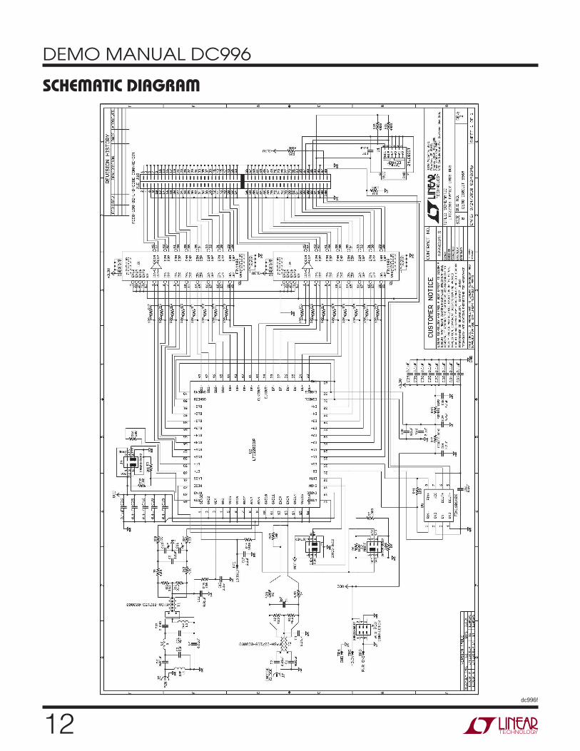
SCHEMATIC DIAGRAM

13dc996f
DEMO MANUAL DC996
Information furnished by Linear Technology Corporation is believed to be accurate and reliable. However, no responsibility is assumed for its use. Linear Technology Corporation makes no representa-tion that the interconnection of its circuits as described herein will not infringe on existing patent rights.
SCHEMATIC DIAGRAM

14dc996f
DEMO MANUAL DC996
Linear Technology Corporation1630 McCarthy Blvd., Milpitas, CA 95035-7417 (408) 432-1900 ● FAX: (408) 434-0507 ● www.linear.com © LINEAR TECHNOLOGY CORPORATION 2012
LT 0512 • PRINTED IN USA
DEMONSTRATION BOARD IMPORTANT NOTICE
Linear Technology Corporation (LTC) provides the enclosed product(s) under the following AS IS conditions:
This demonstration board (DEMO BOARD) kit being sold or provided by Linear Technology is intended for use for ENGINEERING DEVELOPMENT OR EVALUATION PURPOSES ONLY and is not provided by LTC for commercial use. As such, the DEMO BOARD herein may not be complete in terms of required design-, marketing-, and/or manufacturing-related protective considerations, including but not limited to product safety measures typically found in finished commercial goods. As a prototype, this product does not fall within the scope of the European Union directive on electromagnetic compatibility and therefore may or may not meet the technical requirements of the directive, or other regulations.
If this evaluation kit does not meet the specifications recited in the DEMO BOARD manual the kit may be returned within 30 days from the date of delivery for a full refund. THE FOREGOING WARRANTY IS THE EXCLUSIVE WARRANTY MADE BY THE SELLER TO BUYER AND IS IN LIEU OF ALL OTHER WARRANTIES, EXPRESSED, IMPLIED, OR STATUTORY, INCLUDING ANY WARRANTY OF MERCHANTABILITY OR FITNESS FOR ANY PARTICULAR PURPOSE. EXCEPT TO THE EXTENT OF THIS INDEMNITY, NEITHER PARTY SHALL BE LIABLE TO THE OTHER FOR ANY INDIRECT, SPECIAL, INCIDENTAL, OR CONSEQUENTIAL DAMAGES.
The user assumes all responsibility and liability for proper and safe handling of the goods. Further, the user releases LTC from all claims arising from the handling or use of the goods. Due to the open construction of the product, it is the user’s responsibility to take any and all appropriate precautions with regard to electrostatic discharge. Also be aware that the products herein may not be regulatory compliant or agency certified (FCC, UL, CE, etc.).
No License is granted under any patent right or other intellectual property whatsoever. LTC assumes no liability for applications assistance, customer product design, software performance, or infringement of patents or any other intellectual property rights of any kind.
LTC currently services a variety of customers for products around the world, and therefore this transaction is not exclusive.
Please read the DEMO BOARD manual prior to handling the product. Persons handling this product must have electronics training and observe good laboratory practice standards. Common sense is encouraged.
This notice contains important safety information about temperatures and voltages. For further safety concerns, please contact a LTC application engineer.
Mailing Address:
Linear Technology
1630 McCarthy Blvd.
Milpitas, CA 95035
Copyright © 2004, Linear Technology Corporation