Embed Size (px)
Citation preview
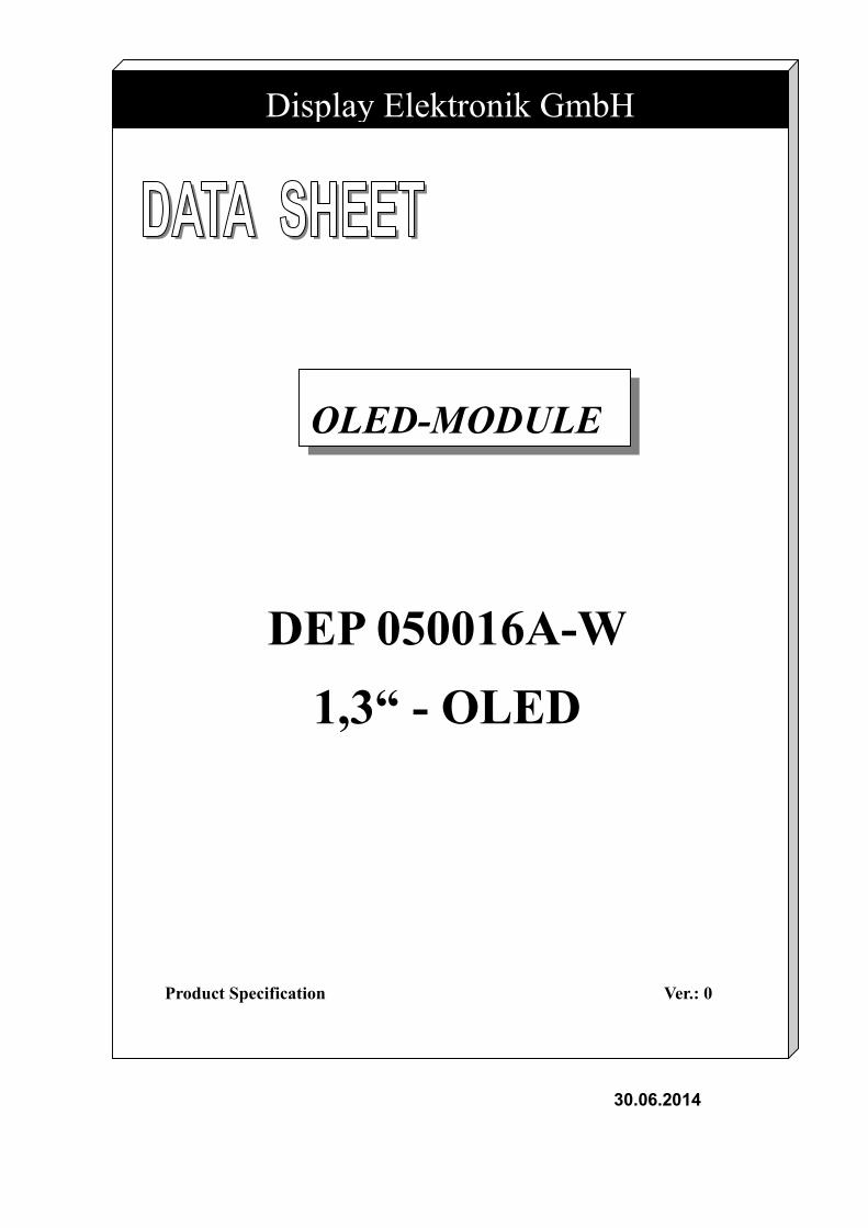
30.06.2014
Display Elektronik GmbH
DEP 050016A-W 1,3“ - OLED
OLED-MODULE
Product Specification Ver.: 0
DEP 050016A-W Production Specification
Version: 0 PAGE: 2
Revision History
VERSION DATE REVISED PAGE NO. Note
0 30.06.2014 First release
DEP 050016A-W Production Specification
Version: 0 PAGE: 3
Contents 1. General Specification
2. Interface Pin Function
3. Counter Drawing & Block Diagram
4. Absolute Maximum Ratings
5. Electrical Characteristics
6. Optical Characteristics
7. OLED Lifetime
8. Reliability
9. Inspection specification
10. Precautions in use of OLED Modules
DEP 050016A-W Production Specification
Version: 0 PAGE: 4
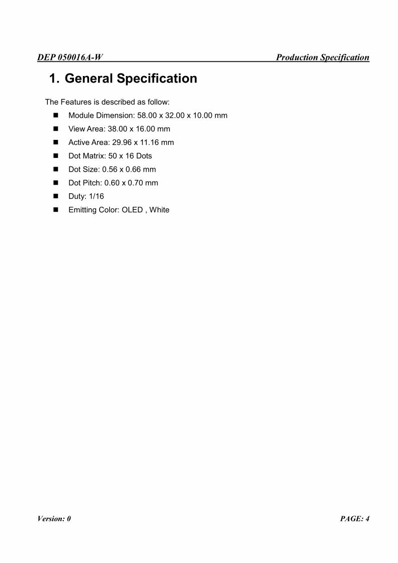
1. General Specification The Features is described as follow:
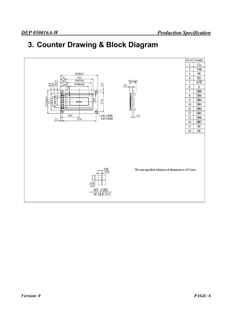
n Module Dimension: 58.00 x 32.00 x 10.00 mm
n View Area: 38.00 x 16.00 mm
n Active Area: 29.96 x 11.16 mm
n Dot Matrix: 50 x 16 Dots
n Dot Size: 0.56 x 0.66 mm
n Dot Pitch: 0.60 x 0.70 mm
n Duty: 1/16
n Emitting Color: OLED , White
DEP 050016A-W Production Specification
Version: 0 PAGE: 5
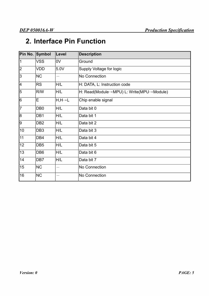
2. Interface Pin Function Pin No. Symbol Level Description
1 VSS 0V Ground
2 VDD 5.0V Supply Voltage for logic
3 NC - No Connection
4 RS H/L H: DATA, L: Instruction code
5 R/W H/L H: Read(Module→MPU) L: Write(MPU→Module)
6 E H,H→L Chip enable signal
7 DB0 H/L Data bit 0
8 DB1 H/L Data bit 1
9 DB2 H/L Data bit 2
10 DB3 H/L Data bit 3
11 DB4 H/L Data bit 4
12 DB5 H/L Data bit 5
13 DB6 H/L Data bit 6
14 DB7 H/L Data bit 7
15 NC - No Connection
16 NC - No Connection
DEP 050016A-W Production Specification
Version: 0 PAGE: 6
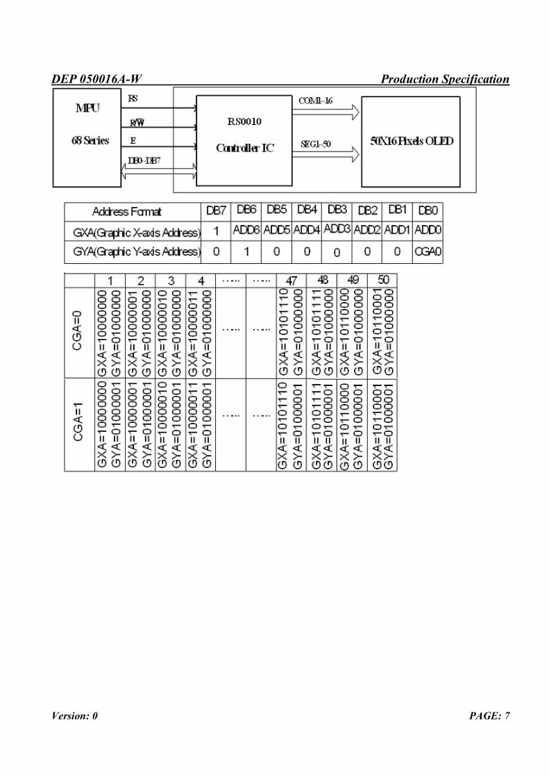
3. Counter Drawing & Block Diagram
DEP 050016A-W Production Specification
Version: 0 PAGE: 7
DEP 050016A-W Production Specification
Version: 0 PAGE: 8
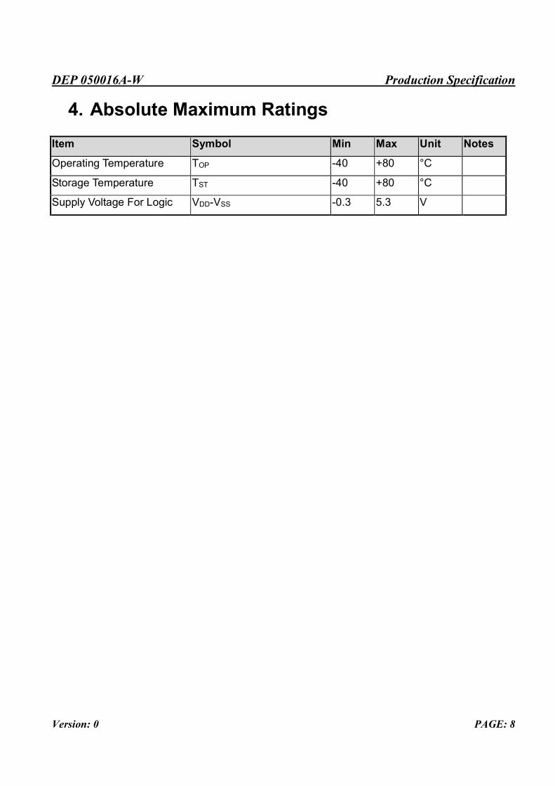
4. Absolute Maximum Ratings Item Symbol Min Max Unit Notes
Operating Temperature TOP -40 +80 °C
Storage Temperature TST -40 +80 °C
Supply Voltage For Logic VDD-VSS -0.3 5.3 V
DEP 050016A-W Production Specification
Version: 0 PAGE: 9
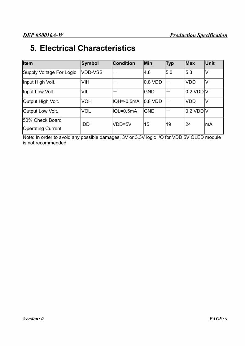
5. Electrical Characteristics Item Symbol Condition Min Typ Max Unit
Supply Voltage For Logic VDD-VSS - 4.8 5.0 5.3 V
Input High Volt. VIH - 0.8 VDD - VDD V
Input Low Volt. VIL - GND - 0.2 VDD V
Output High Volt. VOH IOH=-0.5mA 0.8 VDD - VDD V
Output Low Volt. VOL IOL=0.5mA GND - 0.2 VDD V
50% Check Board
Operating Current IDD VDD=5V 15 19 24 mA
Note: In order to avoid any possible damages, 3V or 3.3V logic I/O for VDD 5V OLED module is not recommended.
DEP 050016A-W Production Specification
Version: 0 PAGE: 10
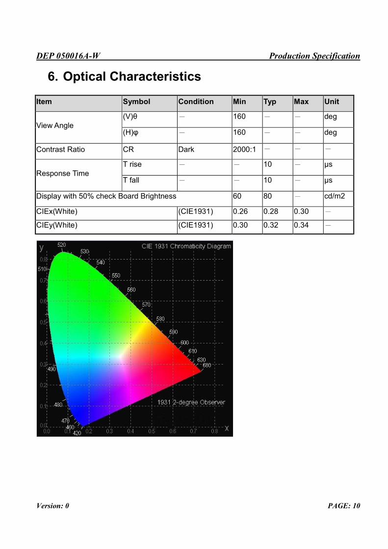
6. Optical Characteristics
Item Symbol Condition Min Typ Max Unit
View Angle (V)θ - 160 - - deg
(H)φ - 160 - - deg
Contrast Ratio CR Dark 2000:1 - - -
Response Time T rise - - 10 - μs
T fall - - 10 - μs
Display with 50% check Board Brightness 60 80 - cd/m2
CIEx(White) (CIE1931) 0.26 0.28 0.30 -
CIEy(White) (CIE1931) 0.30 0.32 0.34 -
DEP 050016A-W Production Specification
Version: 0 PAGE: 11
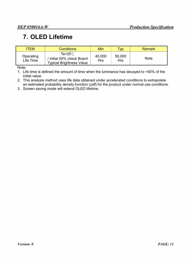
7. OLED Lifetime
ITEM Conditions Min Typ Remark
Operating Life Time
Ta=25℃ / Initial 50% check Board Typical Brightness Value
40,000 Hrs
50,000 Hrs Note
Note: 1. Life time is defined the amount of time when the luminance has decayed to <50% of the
initial value. 2. This analysis method uses life data obtained under accelerated conditions to extrapolate
an estimated probability density function (pdf) for the product under normal use conditions. 3. Screen saving mode will extend OLED lifetime.
DEP 050016A-W Production Specification
Version: 0 PAGE: 12
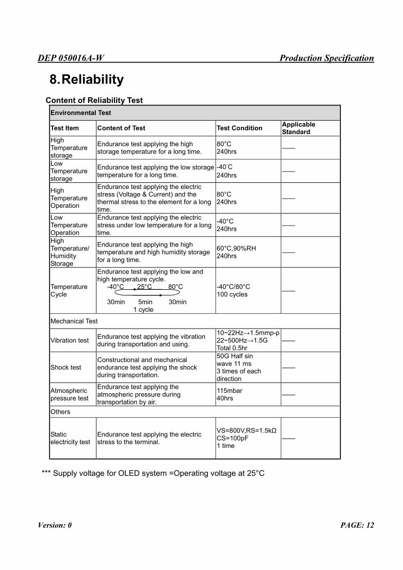
8. Reliability
Content of Reliability Test Environmental Test
Test Item Content of Test Test Condition Applicable Standard
High Temperature storage
Endurance test applying the high storage temperature for a long time.
80°C 240hrs ——
Low Temperature storage
Endurance test applying the low storage temperature for a long time.
-40°C 240hrs ——
High Temperature Operation
Endurance test applying the electric stress (Voltage & Current) and the thermal stress to the element for a long time.
80°C 240hrs ——
Low Temperature Operation
Endurance test applying the electric stress under low temperature for a long time.
-40°C 240hrs ——
High Temperature/ Humidity Storage
Endurance test applying the high temperature and high humidity storage for a long time.
60°C,90%RH 240hrs ——
Temperature Cycle
Endurance test applying the low and high temperature cycle. -40°C 25°C 80°C 30min 5min 30min 1 cycle
-40°C/80°C 100 cycles ——
Mechanical Test
Vibration test Endurance test applying the vibration during transportation and using.
10~22Hz→1.5mmp-p 22~500Hz→1.5G Total 0.5hr
——
Shock test Constructional and mechanical endurance test applying the shock during transportation.
50G Half sin wave 11 ms 3 times of each direction
——
Atmospheric pressure test
Endurance test applying the atmospheric pressure during transportation by air.
115mbar 40hrs ——
Others
Static electricity test
Endurance test applying the electric stress to the terminal.
VS=800V,RS=1.5kΩ CS=100pF 1 time
——
*** Supply voltage for OLED system =Operating voltage at 25°C
DEP 050016A-W Production Specification
Version: 0 PAGE: 13
Test and measurement conditions 1. All measurements shall not be started until the specimens attain to temperature stability.
After the completion of the described reliability test, the samples were left at room temperature for 2 hrs prior to conducting the failure test at 23±5°C; 55±15% RH.
2. All-pixels-on is used as operation test pattern. 3. The degradation of Polarizer are ignored for High Temperature storage, High Temperature/
Humidity Storage, Temperature Cycle Evaluation criteria 1. The function test is OK. 2. No observable defects. 3. Luminance: > 50% of initial value. 4. Current consumption: within ± 50% of initial value. APPENDIX: RESIDUE IMAGE Because the pixels are lighted in different time, the luminance of active pixels may reduce or differ from inactive pixels. Therefore, the residue image will occur. To avoid the residue image, every pixel needs to be lighted up uniformly.
DEP 050016A-W Production Specification
Version: 0 PAGE: 14
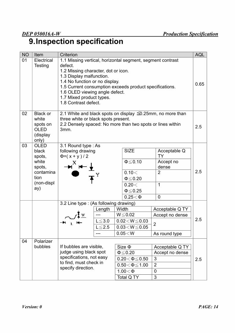
9. Inspection specification NO Item Criterion AQL 01 Electrical
Testing 1.1 Missing vertical, horizontal segment, segment contrast defect. 1.2 Missing character, dot or icon. 1.3 Display malfunction. 1.4 No function or no display. 1.5 Current consumption exceeds product specifications. 1.6 OLED viewing angle defect. 1.7 Mixed product types. 1.8 Contrast defect.
0.65
02 Black or white spots on OLED (display only)
2.1 White and black spots on display ≦0.25mm, no more than three white or black spots present. 2.2 Densely spaced: No more than two spots or lines within 3mm. 2.5
03 OLED black spots, white spots, contamination (non-display)
3.1 Round type : As following drawing Φ=( x + y ) / 2
SIZE Acceptable Q TY
Φ≦0.10 Accept no dense
0.10<Φ≦0.20
2
0.20<Φ≦0.25
1
0.25<Φ 0
2.5
3.2 Line type : (As following drawing)
Length Width Acceptable Q TY --- W≦0.02 Accept no dense L≦3.0 0.02<W≦0.03
2 L≦2.5 0.03<W≦0.05 --- 0.05<W As round type
2.5
04 Polarizer bubbles
If bubbles are visible, judge using black spot specifications, not easy to find, must check in specify direction.
Size Φ Acceptable Q TY Φ≦0.20 Accept no dense 0.20<Φ≦0.50 3 0.50<Φ≦1.00 2 1.00<Φ 0 Total Q TY 3
2.5
DEP 050016A-W Production Specification
Version: 0 PAGE: 15
NO Item Criterion AQL 05 Scratches Follow NO.3 OLED black spots, white spots, contamination
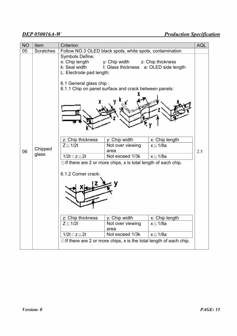
06 Chipped glass
Symbols Define: x: Chip length y: Chip width z: Chip thickness k: Seal width t: Glass thickness a: OLED side length L: Electrode pad length: 6.1 General glass chip : 6.1.1 Chip on panel surface and crack between panels:
z: Chip thickness y: Chip width x: Chip length Z≦1/2t Not over viewing
area x≦1/8a
1/2t<z≦2t Not exceed 1/3k x≦1/8a ☉If there are 2 or more chips, x is total length of each chip. 6.1.2 Corner crack:
z: Chip thickness y: Chip width x: Chip length Z≦1/2t Not over viewing
area x≦1/8a
1/2t<z≦2t Not exceed 1/3k x≦1/8a ☉If there are 2 or more chips, x is the total length of each chip.
2.5
DEP 050016A-W Production Specification
Version: 0 PAGE: 16
NO Item Criterion AQL
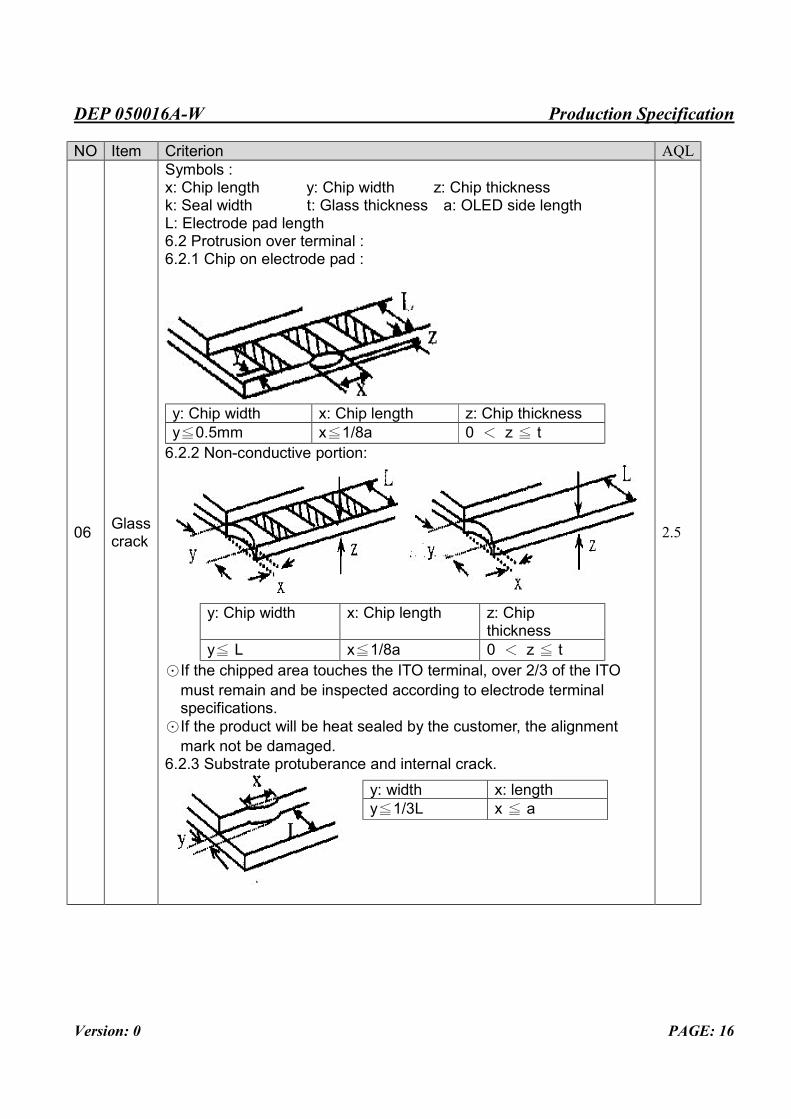
06 Glass crack
Symbols : x: Chip length y: Chip width z: Chip thickness k: Seal width t: Glass thickness a: OLED side length L: Electrode pad length 6.2 Protrusion over terminal : 6.2.1 Chip on electrode pad :
y: Chip width x: Chip length z: Chip thickness y≦0.5mm x≦1/8a 0 < z ≦ t
6.2.2 Non-conductive portion:
y: Chip width x: Chip length z: Chip
thickness y≦ L x≦1/8a 0 < z ≦ t
☉If the chipped area touches the ITO terminal, over 2/3 of the ITO must remain and be inspected according to electrode terminal specifications. ☉If the product will be heat sealed by the customer, the alignment
mark not be damaged. 6.2.3 Substrate protuberance and internal crack.
y: width x: length y≦1/3L x ≦ a
2.5
DEP 050016A-W Production Specification
Version: 0 PAGE: 17
NO Item Criterion AQL
07 Cracked glass The OLED with extensive crack is not acceptable. 2.5
08 Backlight elements
8.1 Illumination source flickers when lit. 8.2 Spots or scratched that appear when lit must be judged.
Using OLED spot, lines and contamination standards. 8.3 Backlight doesn’t light or color wrong.
0.65 2.5 0.65
09 Bezel
9.1 Bezel may not have rust, be deformed or have
fingerprints, stains or other contamination. 9.2 Bezel must comply with job specifications.
2.5 0.65
10 PCB、COB
10.1 COB seal may not have pinholes larger than 0.2mm or
contamination. 10.2 COB seal surface may not have pinholes through to the
IC. 10.3 The height of the COB should not exceed the height
indicated in the assembly diagram. 10.4 There may not be more than 2mm of sealant outside the
seal area on the PCB. And there should be no more than three places.
10.5 No oxidation or contamination PCB terminals. 10.6 Parts on PCB must be the same as on the production
characteristic chart. There should be no wrong parts, missing parts or excess parts.
10.7 The jumper on the PCB should conform to the product characteristic chart.
10.8 If solder gets on bezel tab pads, OLED pad, zebra pad or screw hold pad, make sure it is smoothed down.
2.5 2.5 0.65 2.5 2.5 0.65 0.65 2.5
11 Soldering
11.1 No un-melted solder paste may be present on the PCB. 11.2 No cold solder joints, missing solder connections,
oxidation or icicle. 11.3 No residue or solder balls on PCB. 11.4 No short circuits in components on PCB.
2.5 2.5 2.5 0.65
DEP 050016A-W Production Specification
Version: 0 PAGE: 18
NO Item Criterion AQL
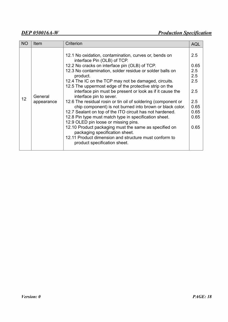
12 General appearance
12.1 No oxidation, contamination, curves or, bends on
interface Pin (OLB) of TCP. 12.2 No cracks on interface pin (OLB) of TCP. 12.3 No contamination, solder residue or solder balls on
product. 12.4 The IC on the TCP may not be damaged, circuits. 12.5 The uppermost edge of the protective strip on the
interface pin must be present or look as if it cause the interface pin to sever.
12.6 The residual rosin or tin oil of soldering (component or chip component) is not burned into brown or black color.
12.7 Sealant on top of the ITO circuit has not hardened. 12.8 Pin type must match type in specification sheet. 12.9 OLED pin loose or missing pins. 12.10 Product packaging must the same as specified on
packaging specification sheet. 12.11 Product dimension and structure must conform to
product specification sheet.
2.5 0.65 2.5 2.5 2.5 2.5 2.5 0.65 0.65 0.65 0.65
DEP 050016A-W Production Specification
Version: 0 PAGE: 19
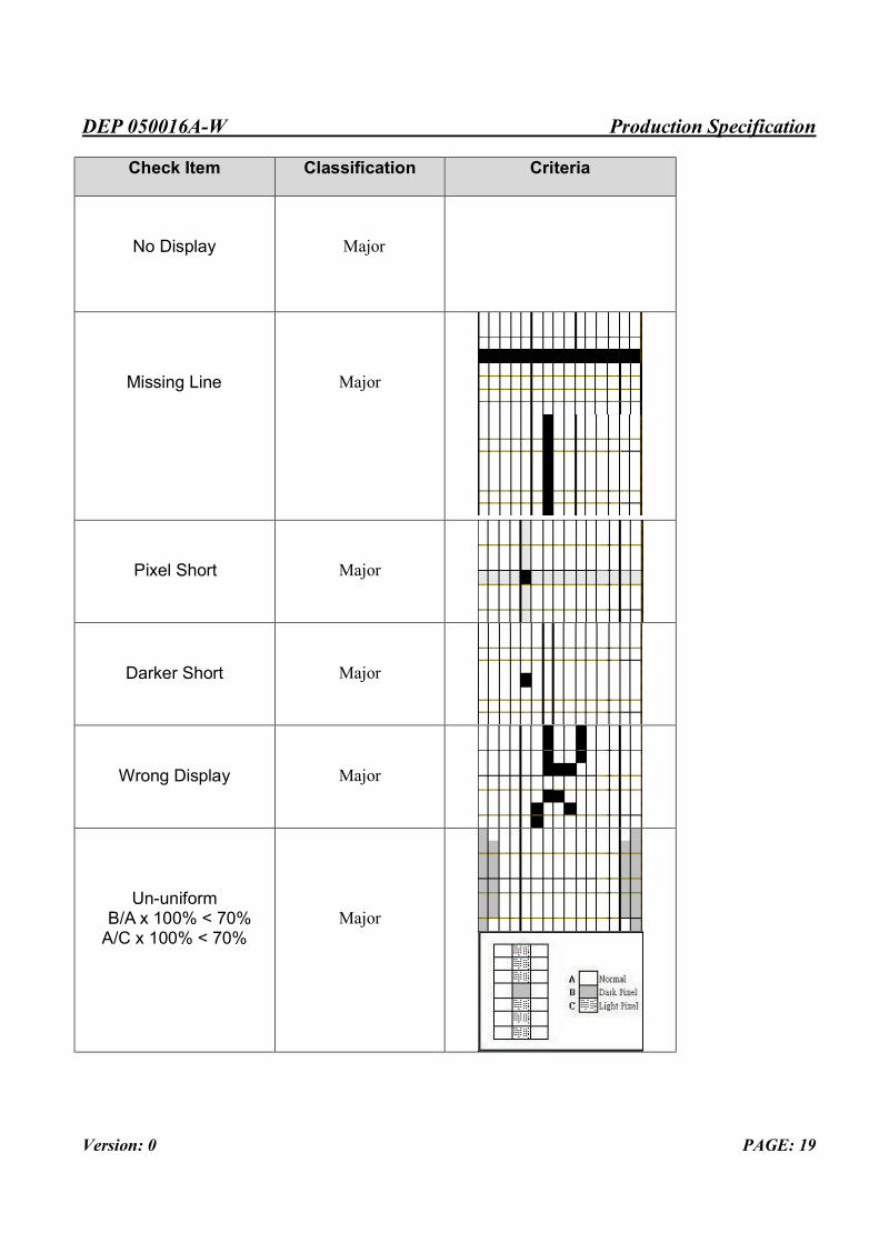
Check Item Classification Criteria
No Display
Major
Missing Line
Major
Pixel Short
Major
Darker Short
Major
Wrong Display
Major
Un-uniform B/A x 100% < 70%
A/C x 100% < 70%
Major
DEP 050016A-W Production Specification
Version: 0 PAGE: 20
10. Precautions in use of OLED Modules (1) Avoid applying excessive shocks to module or making any alterations or modifications to it. (2) Don’t make extra holes on the printed circuit board, modify its shape or change the
components of OLED display module. (3) Don’t disassemble the OLED display module. (4) Don’t operate it above the absolute maximum rating. (5) Don’t drop, bend or twist OLED display module. (6) Soldering: only to the I/O terminals. (7) Storage: please storage in anti-static electricity container and clean environment. (8) It's pretty common to use "Screen Saver" to extend the lifetime and Don't use fix
information for long time in real application. (9) Don't use fixed information in OLED panel for long time, that will extend "screen burn"
effect time.. (10) DISPLAY has the right to change the passive components, including R2and R3 adjust
resistors. (Resistors, capacitors and other passive components will have different appearance and color caused by the different supplier.)
(11) DISPLAY have the right to change the PCB Rev. (In order to satisfy the supplying stability, management optimization and the best product performance...etc, under the premise of not affecting the electrical characteristics and external dimensions, DISPLAY have the right to modify the version.) 10.1 Handling Precautions (1) Since the display panel is being made of glass, do not apply mechanical impacts such us
dropping from a high position. (2) If the display panel is broken by some accident and the internal organic substance leaks
out, be careful not to inhale nor lick the organic substance. (3) If pressure is applied to the display surface or its neighborhood of the OLED display
module, the cell structure may be damaged and be careful not to apply pressure to these sections.
(4) The polarizer covering the surface of the OLED display module is soft and easily scratched. Please be careful when handling the OLED display module.
(5) When the surface of the polarizer of the OLED display module has soil, clean the surface. It takes advantage of by using following adhesion tape.
* Scotch Mending Tape No. 810 or an equivalent Never try to breathe upon the soiled surface nor wipe the surface using cloth containing solvent Also, pay attention that the following liquid and solvent may spoil the polarizer: * Water * Ketone * Aromatic Solvents (6) Hold OLED display module very carefully when placing OLED display module into the
System housing. Do not apply excessive stress or pressure to OLED display module. And, do not over bend the film with electrode pattern layouts. These stresses will influence the display performance. Also, secure sufficient rigidity for the outer cases.
DEP 050016A-W Production Specification
Version: 0 PAGE: 21
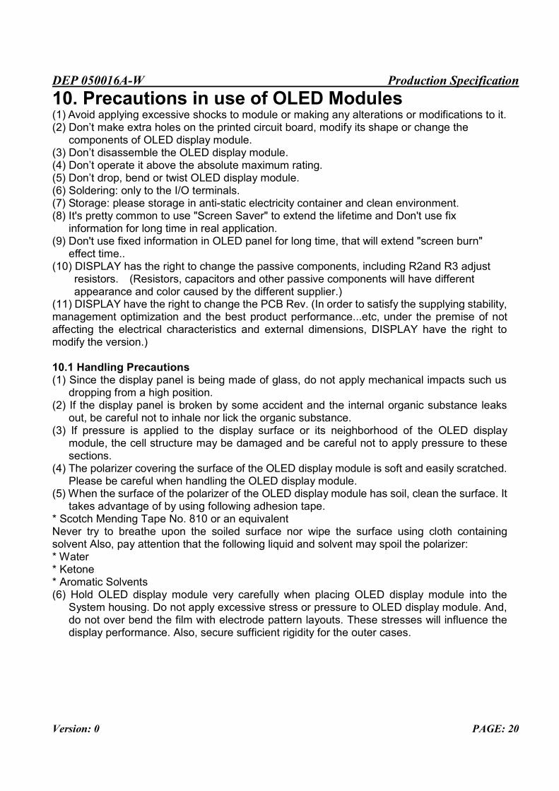
(7) Do not apply stress to the LSI chips and the surrounding molded sections. (8) Do not disassemble nor modify the OLED display module. (9) Do not apply input signals while the logic power is off. (10) Pay sufficient attention to the working environments when handing OLED display modules
to prevent occurrence of element breakage accidents by static electricity. * Be sure to make human body grounding when handling OLED display modules. * Be sure to ground tools to use or assembly such as soldering irons. * To suppress generation of static electricity, avoid carrying out assembly work under dry
environments. * Protective film is being applied to the surface of the display panel of the OLED display module. Be careful since static electricity may be generated when exfoliating the protective film.
(11) Protection film is being applied to the surface of the display panel and removes the protection film before assembling it. At this time, if the OLED display module has been stored surface of the display panel after removed of the film. In such case, remove the residue material by the method introduced in the above Section 5.
(12) If electric current is applied when the OLED display module is being dewed or when it is placed under high humidity environments, the electrodes may be corroded and be careful to avoid the above.
10.2 Storage Precautions (1) When storing OLED display modules, put them in static electricity preventive bags avoiding
exposure to direct sun light nor to lights of fluorescent lamps. And, also, avoiding high temperature and high humidity environment or low temperature (less than 0°C) environments. (We recommend you to store these modules in the packaged state when they were shipped from DISPLAY. At that time, be careful not to let water drops adhere to the packages or bags nor let dewing occur with them.
(2) If electric current is applied when water drops are adhering to the surface of the OLED display module, when the OLED display module is being dewed or when it is placed under high humidity environments, the electrodes may be corroded and be careful about the above.
DEP 050016A-W Production Specification
Version: 0 PAGE: 22
10.3 Designing Precautions (1) The absolute maximum ratings are the ratings which cannot be exceeded for OLED display
module, and if these values are exceeded, panel damage may be happen. (2) To prevent occurrence of malfunctioning by noise, pay attention to satisfy the VIL and VIH
specifications and, at the same time, to make the signal line cable as short as possible. (3) We recommend you to install excess current preventive unit (fuses, etc.) to the power
circuit (VDD). (Recommend value: 0.5A) (4) Pay sufficient attention to avoid occurrence of mutual noise interference with the neighboring devices. (5) As for EMI, take necessary measures on the equipment side basically. (6) When fastening the OLED display module, fasten the external plastic housing section. (7) If power supply to the OLED display module is forcibly shut down by such errors as taking
out the main battery while the OLED display panel is in operation, we cannot guarantee the quality of this OLED display module. Connection (contact) to any other potential than the above may lead to rupture of the IC.