Embed Size (px)
Citation preview
Deposition of Multilayer Optical Coatings Using Closed Field Magnetron Sputtering
D. R. Gibson, I. Brinkley and E. M. WaddellApplied Multilayers LLC, 1801 SE Commerce Avenue, Battle Ground, WA 98604 United States
ABSTRACT
“Closed field” magnetron (CFM) sputtering offers a flexible and high throughput deposition process for optical coatings and thin films required in display technologies. CFM sputtering uses two or more different metal targets to deposit multilayers comprising a wide range of dielectrics, metals and conductive oxides. Moreover, CFM provides a room temperature deposition process with high ion current density, low bias voltage and reactive oxidation in the entire volume around the rotating substrate drum carrier, thereby producing films over a large surface area at high deposition rate with excellent and reproducible optical properties. Machines based on the Closed Field are scalable to meet a range of batch and in-line size requirements. Typically, thin film thickness control to <±1% is accomplished simply using time, although optical monitoring can be used for more demanding applications. Fine layer thickness control and deposition of graded index layers is also assisted with a specially designed rotating shutter mechanism. This paper presents data on optical properties for CFM deposited optical coatings, including anti-reflection, IR blocker and color control and thermal control filters, graded coatings, narrow band filters as well as conductive transparent oxides such as indium tin oxide. Benefits of the CFM sputter process are described. 1. INTRODUCTION
Multilayer optical coatings are important in a number of applications including precision optics, fiber optical telecommunications and ophthalmic lenses. Optical coatings include anti-reflection coatings to maximize transmission and minimize glare, blocking filters to control exposure to IR and/or UV; edge and notch filters to control color contrast; transparent conductive oxides for use as transparent electrodes or anti-static control and metals as reflective layers. Traditionally, physical vapor deposition techniques are utilized including electron beam deposition and evaporation. Sputter physical vapor deposition is emerging as a preferred alternative for deposition of optical coatings.
Magnetron sputtering has a number of advantages over conventional physical vapor deposition techniques such as electron beam and thermal evaporation. For example, the kinetic energy of the sputtered atoms is typically 10 times higher than that of evaporated species, this results in much harder and much more adherent coatings. The energy of the process also removes the need for substrate heating during deposition which is of specific benefit when coating plastic substrates or other temperature sensitive substrate materials. This means that deposition is carried out at room temperature allowing different materials such as glass and plastic to be coated even in the same batch. Compact magnetron sources are also capable of high deposition rates which result in fast process cycle times.
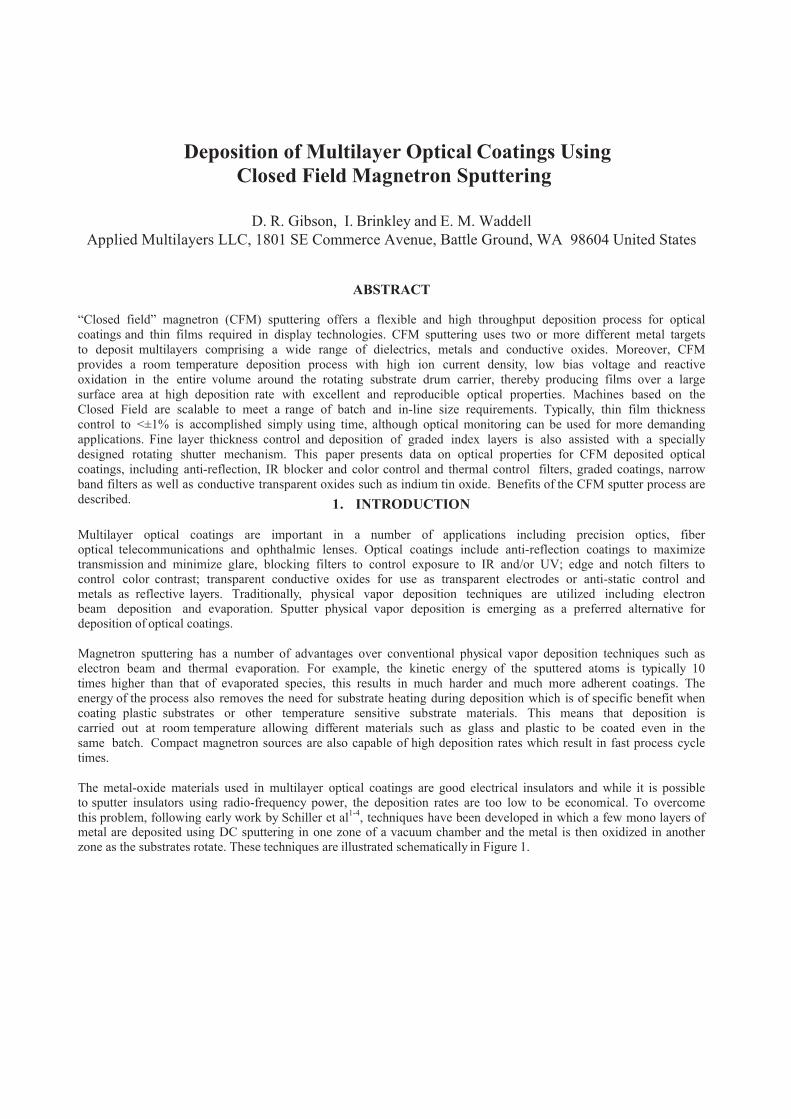
The metal-oxide materials used in multilayer optical coatings are good electrical insulators and while it is possible to sputter insulators using radio-frequency power, the deposition rates are too low to be economical. To overcome this problem, following early work by Schiller et al1-4, techniques have been developed in which a few mono layers of metal are deposited using DC sputtering in one zone of a vacuum chamber and the metal is then oxidized in another zone as the substrates rotate. These techniques are illustrated schematically in Figure 1.
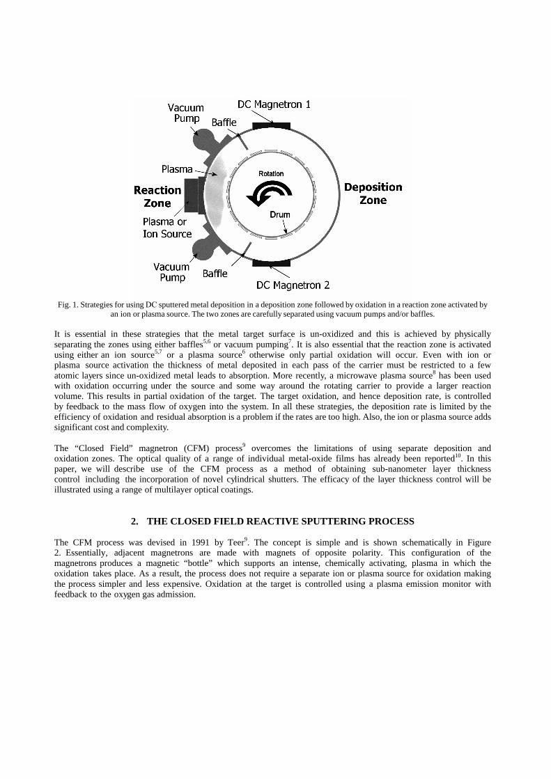
Fig. 1. Strategies for using DC sputtered metal deposition in a deposition zone followed by oxidation in a reaction zone activated byan ion or plasma source. The two zones are carefully separated using vacuum pumps and/or baffles.
It is essential in these strategies that the metal target surface is un-oxidized and this is achieved by physically separating the zones using either baffles5,6 or vacuum pumping7. It is also essential that the reaction zone is activated using either an ion source5,7 or a plasma source6 otherwise only partial oxidation will occur. Even with ion or plasma source activation the thickness of metal deposited in each pass of the carrier must be restricted to a few atomic layers since un-oxidized metal leads to absorption. More recently, a microwave plasma source8 has been used with oxidation occurring under the source and some way around the rotating carrier to provide a larger reaction volume. This results in partial oxidation of the target. The target oxidation, and hence deposition rate, is controlled by feedback to the mass flow of oxygen into the system. In all these strategies, the deposition rate is limited by the efficiency of oxidation and residual absorption is a problem if the rates are too high. Also, the ion or plasma source adds significant cost and complexity.
The “Closed Field” magnetron (CFM) process9 overcomes the limitations of using separate deposition and oxidation zones. The optical quality of a range of individual metal-oxide films has already been reported10. In this paper, we will describe use of the CFM process as a method of obtaining sub-nanometer layer thickness control including the incorporation of novel cylindrical shutters. The efficacy of the layer thickness control will be illustrated using a range of multilayer optical coatings.
2. THE CLOSED FIELD REACTIVE SPUTTERING PROCESS
The CFM process was devised in 1991 by Teer9. The concept is simple and is shown schematically in Figure 2. Essentially, adjacent magnetrons are made with magnets of opposite polarity. This configuration of themagnetrons produces a magnetic “bottle” which supports an intense, chemically activating, plasma in which theoxidation takes place. As a result, the process does not require a separate ion or plasma source for oxidation makingthe process simpler and less expensive. Oxidation at the target is controlled using a plasma emission monitor withfeedback to the oxygen gas admission.
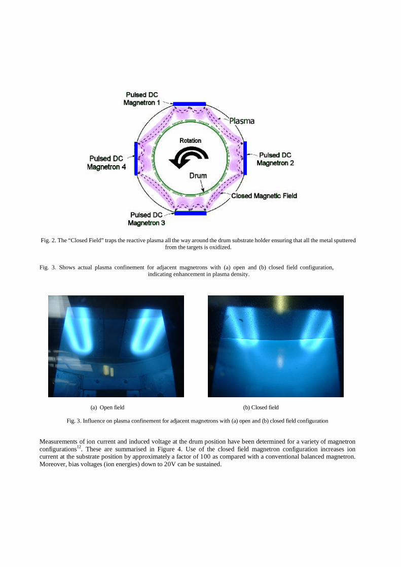
Fig. 2. The “Closed Field” traps the reactive plasma all the way around the drum substrate holder ensuring that all the metal sputtered from the targets is oxidized.
Fig. 3. Shows actual plasma confinement for adjacent magnetrons with (a) open and (b) closed field configuration, indicating enhancement in plasma density.
(a) Open field (b) Closed field
Fig. 3. Influence on plasma confinement for adjacent magnetrons with (a) open and (b) closed field configuration
Measurements of ion current and induced voltage at the drum position have been determined for a variety of magnetronconfigurations12. These are summarised in Figure 4. Use of the closed field magnetron configuration increases ioncurrent at the substrate position by approximately a factor of 100 as compared with a conventional balanced magnetron.Moreover, bias voltages (ion energies) down to 20V can be sustained.
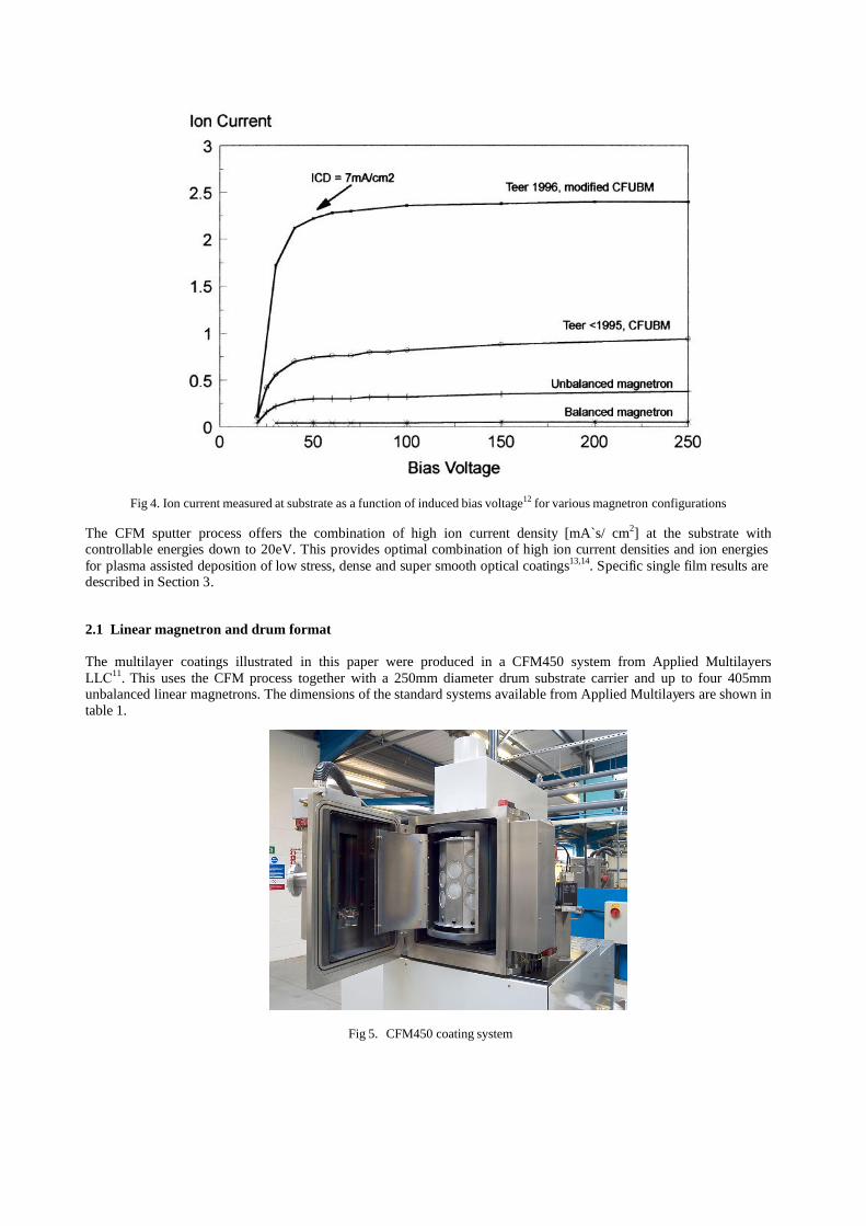
Fig 4. Ion current measured at substrate as a function of induced bias voltage12 for various magnetron configurations
The CFM sputter process offers the combination of high ion current density [mA`s/ cm2] at the substrate with controllable energies down to 20eV. This provides optimal combination of high ion current densities and ion energies for plasma assisted deposition of low stress, dense and super smooth optical coatings13,14. Specific single film results are described in Section 3.
2.1 Linear magnetron and drum format
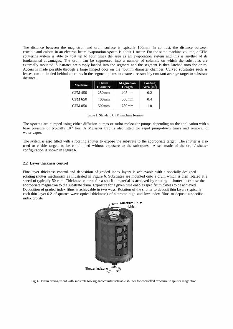
The multilayer coatings illustrated in this paper were produced in a CFM450 system from Applied Multilayers LLC11. This uses the CFM process together with a 250mm diameter drum substrate carrier and up to four 405mm unbalanced linear magnetrons. The dimensions of the standard systems available from Applied Multilayers are shown in table 1.
Fig 5. CFM450 coating system
The distance between the magnetron and drum surface is typically 100mm. In contrast, the distance between crucible and calotte in an electron beam evaporation system is about 1 meter. For the same machine volume, a CFM sputtering system is able to coat up to four times the area as an evaporation system and this is another of its fundamental advantages. The drum can be segmented into a number of columns on which the substrates are externally mounted. Substrates are simply loaded into the segment and the segment is then latched onto the drum. Access is made possible through a large hinged door on the 450mm diameter chamber. Curved substrates such as lenses can be loaded behind apertures in the segment plates to ensure a reasonably constant average target to substrate distance.
Machine DrumDiameter
MagnetronLength
CoatingArea [m2]
CFM 450 250mm 405mm 0.2
CFM 650 400mm 600mm 0.4
CFM 850 500mm 780mm 1.0
Table 1. Standard CFM machine formats
The systems are pumped using either diffusion pumps or turbo molecular pumps depending on the application with a base pressure of typically 10-6 torr. A Meissner trap is also fitted for rapid pump-down times and removal of water vapor.
The system is also fitted with a rotating shutter to expose the substrate to the appropriate target. The shutter is also used to enable targets to be conditioned without exposure to the substrates. A schematic of the drum/ shutter configuration is shown in Figure 6.
2.2 Layer thickness control
Fine layer thickness control and deposition of graded index layers is achievable with a specially designed rotating shutter mechanism as illustrated in Figure 6. Substrates are mounted onto a drum which is then rotated at a speed of typically 50 rpm. Thickness control for a specific material is achieved by rotating a shutter to expose the appropriate magnetron to the substrate drum. Exposure for a given time enables specific thickness to be achieved. Deposition of graded index films is achievable in two ways. Rotation of the shutter to deposit thin layers (typically each thin layer 0.2 of quarter wave optical thickness) of alternate high and low index films to deposit a specific index profile.
Fig. 6. Drum arrangement with substrate tooling and counter rotatable shutter for controlled exposure to sputter magnetron.
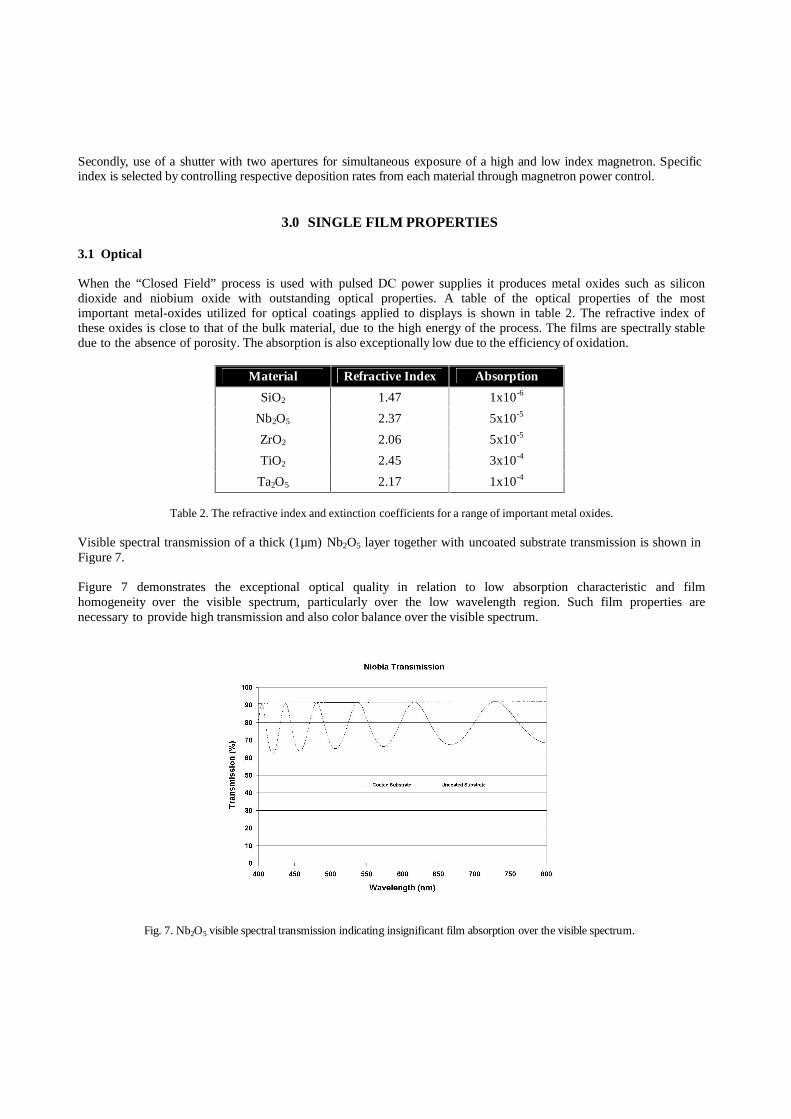
Secondly, use of a shutter with two apertures for simultaneous exposure of a high and low index magnetron. Specific index is selected by controlling respective deposition rates from each material through magnetron power control.
3.0 SINGLE FILM PROPERTIES
3.1 Optical
When the “Closed Field” process is used with pulsed DC power supplies it produces metal oxides such as silicon dioxide and niobium oxide with outstanding optical properties. A table of the optical properties of the most important metal-oxides utilized for optical coatings applied to displays is shown in table 2. The refractive index of these oxides is close to that of the bulk material, due to the high energy of the process. The films are spectrally stable due to the absence of porosity. The absorption is also exceptionally low due to the efficiency of oxidation.
Material Refractive Index AbsorptionSiO2 1.47 1x10⁻⁶
Nb2O5 2.37 5x10⁻⁵
ZrO2 2.06 5x10⁻⁵
TiO2 2.45 3x10⁻⁴
Ta2O5 2.17 1x10⁻⁴
Table 2. The refractive index and extinction coefficients for a range of important metal oxides.
Visible spectral transmission of a thick (1µm) Nb2O5 layer together with uncoated substrate transmission is shown in Figure 7.
Figure 7 demonstrates the exceptional optical quality in relation to low absorption characteristic and film homogeneity over the visible spectrum, particularly over the low wavelength region. Such film properties are necessary to provide high transmission and also color balance over the visible spectrum.
Fig. 7. Nb2O5 visible spectral transmission indicating insignificant film absorption over the visible spectrum.
3.2 Microstructure
Cross sectional electron micrograph showing film structure of a 1um thick niobia film is shown in Figure 8.
Fig. 8. Cross sectional scanning electron micrograph of fractured 1um thick niobia film on glass (courtesy Loughborough University).
Figure 8 illustrates the amorphous film microstructure and smooth surface.
3.3 Surface Topography
Figure 9 shows surface roughness for the thick niobia oxide films measured using coherence correlation interferometry10. Resultsdemonstrate super-smooth films with rms roughness measured at 0.45nm, with no significant roughness increase as compared to theuncoated substrate. Data courtesy of J Armstrong (Taylor Hobson Ltd ).
Fig. 9. Surface roughness of a 1 um thick niobia film measured using white light interferometry10
3.4 Stress
Film stress was evaluated from measured substrate curvature before and after film deposition. Stress was calculated from the Stoney formula15. Curvature was measured along two perpendicular axes across the wafer. Typical values are indicated in Table 3.
Typical measurement error is ±5%.
Material StressSiO2 -150 MPa
Nb2O5 -30MPaZrO2 -80MpaITO -70Mpa
Table 3. Measured stress for a range of oxide films (negative value indicates compressive stress)
The values indicated in Table 3 are significantly lower than values reported recently14 for oxide materials. The lower stress is attributed to lower ion energies and higher ion fluxes provided by the CFM sputter process.
4.0 MULTILAYER OPTICAL COATINGS
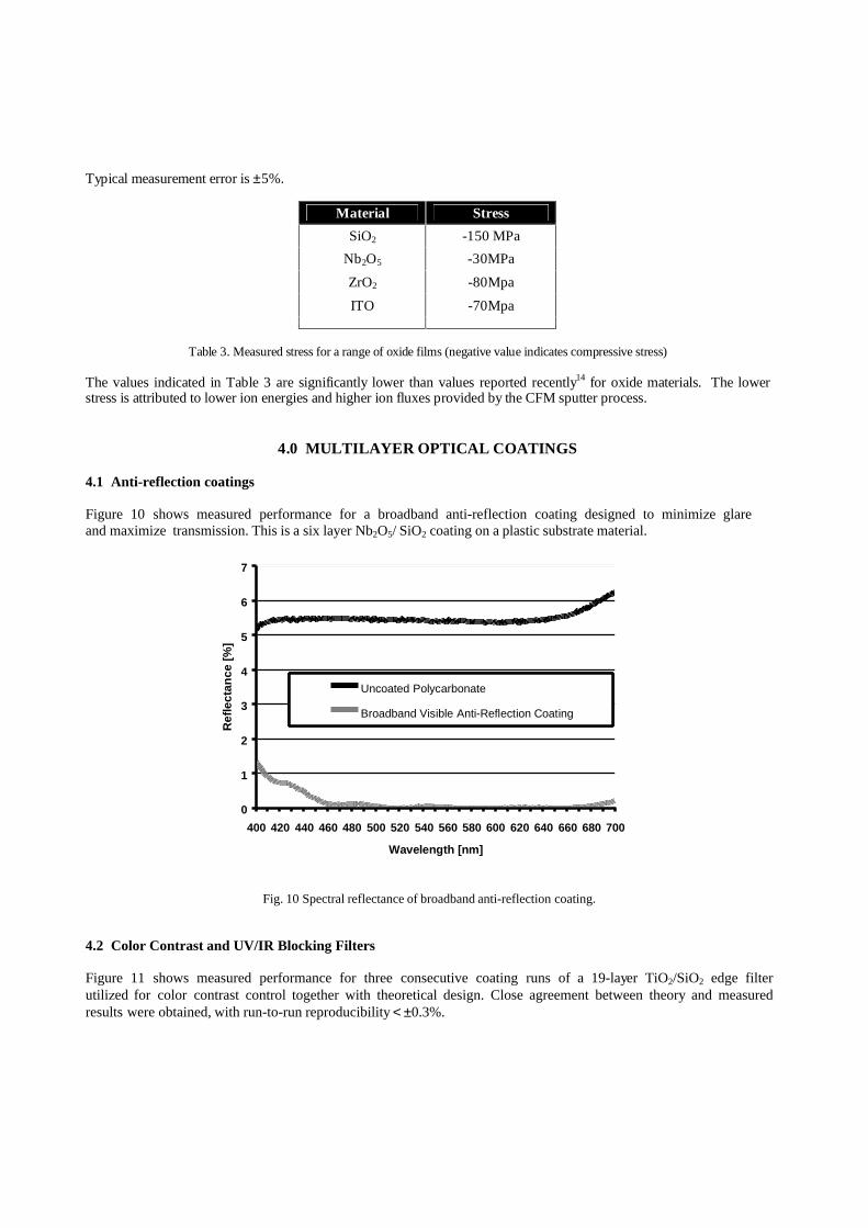
4.1 Anti-reflection coatings
Figure 10 shows measured performance for a broadband anti-reflection coating designed to minimize glare and maximize transmission. This is a six layer Nb2O5/ SiO2 coating on a plastic substrate material.
0
1
2
3
4
5
6
7
400 420 440 460 480 500 520 540 560 580 600 620 640 660 680 700
Wavelength [nm]
Ref
lect
ance
[%]
Uncoated Polycarbonate
Broadband Visible Anti-Reflection Coating
Fig. 10 Spectral reflectance of broadband anti-reflection coating.
4.2 Color Contrast and UV/IR Blocking Filters
Figure 11 shows measured performance for three consecutive coating runs of a 19-layer TiO2/SiO2 edge filter utilized for color contrast control together with theoretical design. Close agreement between theory and measured results were obtained, with run-to-run reproducibility < ±0.3%.
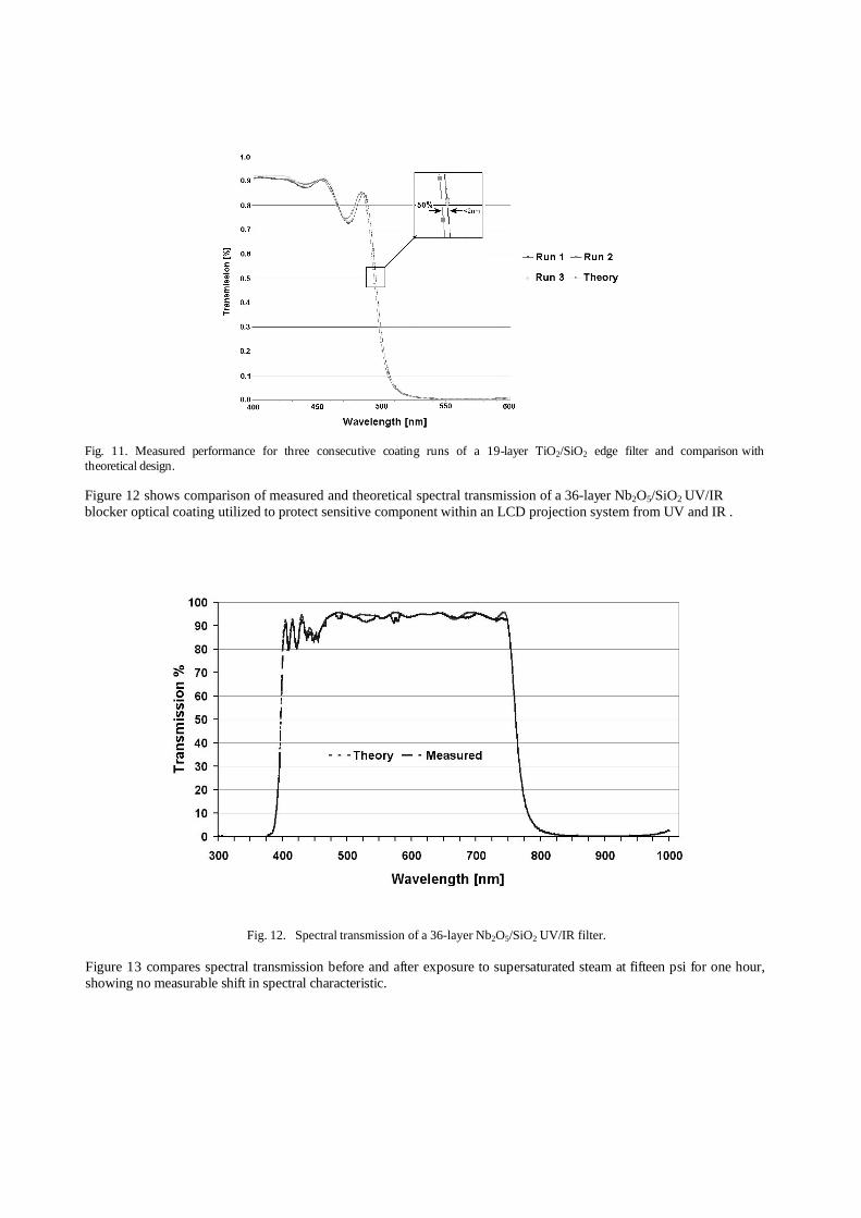
Fig. 11. Measured performance for three consecutive coating runs of a 19-layer TiO2/SiO2 edge filter and comparison with theoretical design.
Figure 12 shows comparison of measured and theoretical spectral transmission of a 36-layer Nb2O5/SiO2 UV/IR blocker optical coating utilized to protect sensitive component within an LCD projection system from UV and IR .
Fig. 12. Spectral transmission of a 36-layer Nb2O5/SiO2 UV/IR filter.
Figure 13 compares spectral transmission before and after exposure to supersaturated steam at fifteen psi for one hour, showing no measurable shift in spectral characteristic.
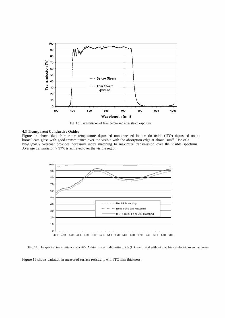
Fig. 13. Transmission of filter before and after steam exposure.
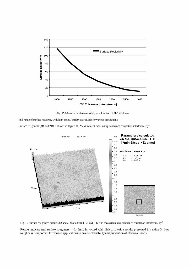
4.3 Transparent Conductive OxidesFigure 14 shows data from room temperature deposited non-annealed indium tin oxide (ITO) deposited on to borosilicate glass with good transmittance over the visible with the absorption edge at about 1um16. Use of a Nb2O5/SiO2 overcoat provides necessary index matching to maximize transmission over the visible spectrum. Average transmission > 97% is achieved over the visible region.
0
1 0
2 0
3 0
4 0
5 0
6 0
7 0
8 0
9 0
10 0
400 420 44 0 460 4 80 5 00 520 54 0 560 5 80 600 620 640 660 680 700
No AR M at ching
Rea r Face AR M atche d
ITO & Rear Face A R Matched
Fig. 14. The spectral transmittance of a 3650A thin film of indium-tin oxide (ITO) with and without matching dielectric overcoat layers.
Figure 15 shows variation in measured surface resistivity with ITO film thickness.
0
20
40
60
80
100
120
140
1000 1500 2000 2500 3000 3500 4000
ITO Thickness [ Angstroms]
Surf
ace
Res
istiv
ity
Surface Resistivity
Fig. 15 Measured surface resistivity as a function of ITO thickness
Full range of surface resistivity with high optical quality is available for various applications.
Surface roughness (3D and 2D) is shown in Figure 16. Measurement made using coherence correlation interferometry10.
Fig. 16 Surface roughness profile [3D and 2D] of a thick (3650A) ITO film measured using coherence correlation interferometry10
Results indicate rms surface roughness = 0.45nm, in accord with dielectric oxide results presented in section 3. Lowroughness is important for various applications to ensure cleanability and prevention of electrical shorts.
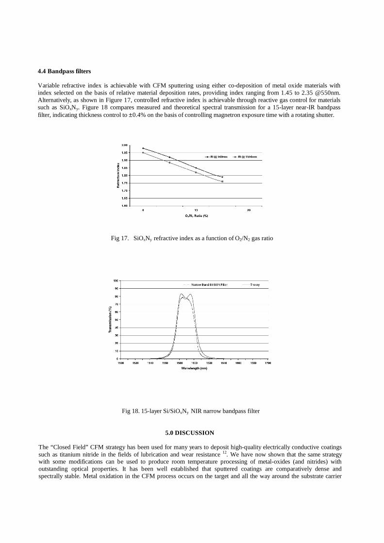
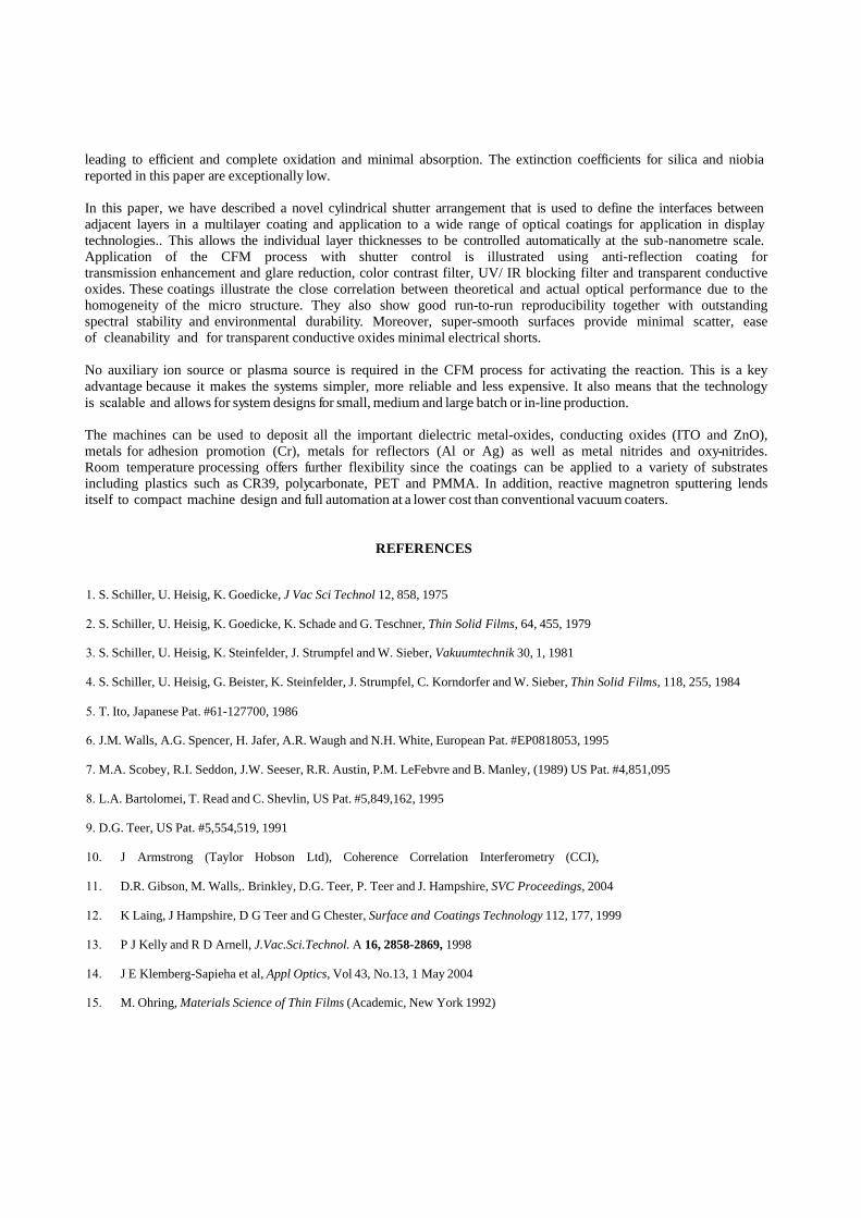
4.4 Bandpass filters
Variable refractive index is achievable with CFM sputtering using either co-deposition of metal oxide materials withindex selected on the basis of relative material deposition rates, providing index ranging from 1.45 to 2.35 @550nm.Alternatively, as shown in Figure 17, controlled refractive index is achievable through reactive gas control for materialssuch as SiOxNy. Figure 18 compares measured and theoretical spectral transmission for a 15-layer near-IR bandpassfilter, indicating thickness control to ±0.4% on the basis of controlling magnetron exposure time with a rotating shutter.
Fig 17. SiOxNy refractive index as a function of O2/N2 gas ratio
Fig 18. 15-layer Si/SiOxNy NIR narrow bandpass filter
5.0 DISCUSSION
The “Closed Field” CFM strategy has been used for many years to deposit high-quality electrically conductive coatings such as titanium nitride in the fields of lubrication and wear resistance 12. We have now shown that the same strategy with some modifications can be used to produce room temperature processing of metal-oxides (and nitrides) with outstanding optical properties. It has been well established that sputtered coatings are comparatively dense and spectrally stable. Metal oxidation in the CFM process occurs on the target and all the way around the substrate carrier
leading to efficient and complete oxidation and minimal absorption. The extinction coefficients for silica and niobia reported in this paper are exceptionally low.
In this paper, we have described a novel cylindrical shutter arrangement that is used to define the interfaces between adjacent layers in a multilayer coating and application to a wide range of optical coatings for application in display technologies.. This allows the individual layer thicknesses to be controlled automatically at the sub-nanometre scale. Application of the CFM process with shutter control is illustrated using anti-reflection coating for transmission enhancement and glare reduction, color contrast filter, UV/ IR blocking filter and transparent conductive oxides. These coatings illustrate the close correlation between theoretical and actual optical performance due to the homogeneity of the micro structure. They also show good run-to-run reproducibility together with outstanding spectral stability and environmental durability. Moreover, super-smooth surfaces provide minimal scatter, ease of cleanability and for transparent conductive oxides minimal electrical shorts.
No auxiliary ion source or plasma source is required in the CFM process for activating the reaction. This is a key advantage because it makes the systems simpler, more reliable and less expensive. It also means that the technology is scalable and allows for system designs for small, medium and large batch or in-line production.
The machines can be used to deposit all the important dielectric metal-oxides, conducting oxides (ITO and ZnO), metals for adhesion promotion (Cr), metals for reflectors (Al or Ag) as well as metal nitrides and oxy-nitrides. Room temperature processing offers further flexibility since the coatings can be applied to a variety of substrates including plastics such as CR39, polycarbonate, PET and PMMA. In addition, reactive magnetron sputtering lends itself to compact machine design and full automation at a lower cost than conventional vacuum coaters.
REFERENCES
1. S. Schiller, U. Heisig, K. Goedicke, J Vac Sci Technol 12, 858, 1975
2. S. Schiller, U. Heisig, K. Goedicke, K. Schade and G. Teschner, Thin Solid Films, 64, 455, 1979
3. S. Schiller, U. Heisig, K. Steinfelder, J. Strumpfel and W. Sieber, Vakuumtechnik 30, 1, 1981
4. S. Schiller, U. Heisig, G. Beister, K. Steinfelder, J. Strumpfel, C. Korndorfer and W. Sieber, Thin Solid Films, 118, 255, 1984
5. T. Ito, Japanese Pat. #61-127700, 1986
6. J.M. Walls, A.G. Spencer, H. Jafer, A.R. Waugh and N.H. White, European Pat. #EP0818053, 1995
7. M.A. Scobey, R.I. Seddon, J.W. Seeser, R.R. Austin, P.M. LeFebvre and B. Manley, (1989) US Pat. #4,851,095
8. L.A. Bartolomei, T. Read and C. Shevlin, US Pat. #5,849,162, 1995
9. D.G. Teer, US Pat. #5,554,519, 1991
10. J Armstrong (Taylor Hobson Ltd), Coherence Correlation Interferometry (CCI),
11. D.R. Gibson, M. Walls,. Brinkley, D.G. Teer, P. Teer and J. Hampshire, SVC Proceedings, 2004
12. K Laing, J Hampshire, D G Teer and G Chester, Surface and Coatings Technology 112, 177, 1999
13. P J Kelly and R D Arnell, J.Vac.Sci.Technol. A 16, 2858-2869, 1998
14. J E Klemberg-Sapieha et al, Appl Optics, Vol 43, No.13, 1 May 2004
15. M. Ohring, Materials Science of Thin Films (Academic, New York 1992)