Embed Size (px)
Citation preview
DML3006LFDS Document number: DS39172 Rev. 3 - 2
1 of 9 www.diodes.com
March 2018 © Diodes Incorporated
DML3006LFDS
NE
W P
RO
DU
CT
AD
VA
NC
E IN
FO
RM
AT
IO
N
AD
VA
NC
ED
IN
FO
RM
AT
IO
N
NE
W P
RO
DU
CT
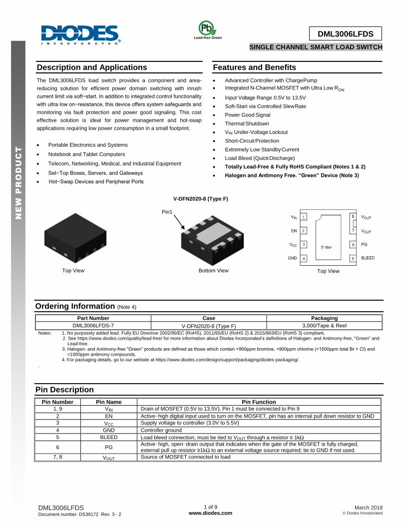
SINGLE CHANNEL SMART LOAD SWITCH
Description and Applications
The DML3006LFDS load switch provides a component and area-
reducing solution for efficient power domain switching with inrush
current limit via soft−start. In addition to integrated control functionality
with ultra low on−resistance, this device offers system safeguards and
monitoring via fault protection and power good signaling. This cost
effective solution is ideal for power management and hot-swap
applications requiring low power consumption in a small footprint.
Portable Electronics and Systems
Notebook and Tablet Computers
Telecom, Networking, Medical, and Industrial Equipment
Set−Top Boxes, Servers, and Gateways
Hot−Swap Devices and Peripheral Ports
Features and Benefits
Advanced Controller with Charge Pump
Integrated N-Channel MOSFET with Ultra Low RON
Input Voltage Range 0.5V to 13.5V
Soft-Start via Controlled Slew Rate
Power Good Signal
Thermal Shutdown
VIN Under-Voltage Lockout
Short-Circuit Protection
Extremely Low Standby Current
Load Bleed (Quick Discharge)
Totally Lead-Free & Fully RoHS Compliant (Notes 1 & 2)
Halogen and Antimony Free. “Green” Device (Note 3)
Ordering Information (Note 4)
Part Number Case Packaging
DML3006LFDS-7 V-DFN2020-8 (Type F) 3,000/Tape & Reel
Notes: 1. No purposely added lead. Fully EU Directive 2002/95/EC (RoHS), 2011/65/EU (RoHS 2) & 2015/863/EU (RoHS 3) compliant. 2. See https://www.diodes.com/quality/lead-free/ for more information about Diodes Incorporated’s definitions of Halogen- and Antimony-free, "Green" and
Lead-free. 3. Halogen- and Antimony-free "Green” products are defined as those which contain <900ppm bromine, <900ppm chlorine (<1500ppm total Br + Cl) and <1000ppm antimony compounds.
4. For packaging details, go to our website at https://www.diodes.com/design/support/packaging/diodes-packaging/.
.
Pin Description
Pin Number Pin Name Pin Function 1, 9 VIN Drain of MOSFET (0.5V to 13.5V), Pin 1 must be connected to Pin 9
2 EN Active−high digital input used to turn on the MOSFET, pin has an internal pull down resistor to GND
3 VCC Supply voltage to controller (3.0V to 5.5V)
4 GND Controller ground
5 BLEED Load bleed connection, must be tied to VOUT through a resistor ≤ 1kΩ
6 PG Active−high, open−drain output that indicates when the gate of the MOSFET is fully charged, external pull up resistor ≥1kΩ to an external voltage source required; tie to GND if not used.
7, 8 VOUT Source of MOSFET connected to load
Bottom View Top View
V-DFN2020-8 (Type F)
Pin1
Top View
DML3006LFDS Document number: DS39172 Rev. 3 - 2
2 of 9 www.diodes.com
March 2018 © Diodes Incorporated
DML3006LFDS
NE
W P
RO
DU
CT
AD
VA
NC
E IN
FO
RM
AT
IO
N
AD
VA
NC
ED
IN
FO
RM
AT
IO
N
NE
W P
RO
DU
CT
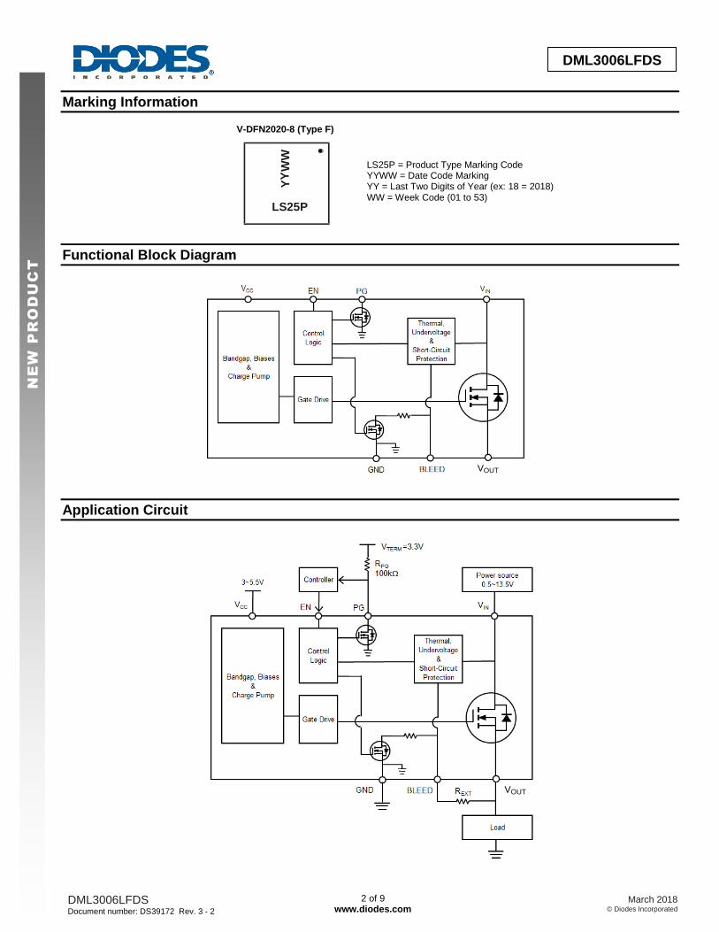
Marking Information
Functional Block Diagram
Application Circuit
VOUT
LS25P = Product Type Marking Code YYWW = Date Code Marking YY = Last Two Digits of Year (ex: 18 = 2018) WW = Week Code (01 to 53)
Y
LS25P
Y
WW
V-DFN2020-8 (Type F)
VOUT
DML3006LFDS Document number: DS39172 Rev. 3 - 2
3 of 9 www.diodes.com
March 2018 © Diodes Incorporated
DML3006LFDS
NE
W P
RO
DU
CT
AD
VA
NC
E IN
FO
RM
AT
IO
N
AD
VA
NC
ED
IN
FO
RM
AT
IO
N
NE
W P
RO
DU
CT
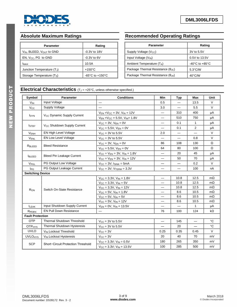
Absolute Maximum Ratings
Parameter Rating
VIN, BLEED, VOUT to GND -0.3V to 18V
EN, VCC, PG to GND -0.3V to 6V
IMAX 10.5A
Junction Temperature (TJ) +150°C
Storage Temperature (TS) -65°C to +150°C
Recommended Operating Ratings
Parameter Rating
Supply Voltage (VCC) 3V to 5.5V
Input Voltage (VIN) 0.5V to 13.5V
Ambient Temperature (TA) -40°C to +85°C
Package Thermal Resistance (θJC) 5.3°C/W
Package Thermal Resistance (θJA) 40°C/W
Electrical Characteristics (TJ = +25°C, unless otherwise specified.)
Symbol Parameter Conditions Min Typ Max Unit
VIN Input Voltage — 0.5 — 13.5 V
VCC Supply Voltage — 3.0 — 5.5 V
IDYN VCC Dynamic Supply Current VEN =VCC = 3V, VIN = 12V — 310 400 µA
VEN =VCC = 5.5V, VIN= 1.8V — 510 750 µA
ISTBY VCC Shutdown Supply Current VCC = 3V, VEN = 0V — 0.1 1 µA
VCC = 5.5V, VEN = 0V — 0.1 2 µA
VENH EN High Level Voltage VCC = 3V to 5.5V 2.0 — — V
VENL EN Low Level Voltage VCC = 3V to 5.5V — — 0.8 V
RBLEED Bleed Resistance VCC = 3V, VEN = 0V 86 108 130 Ω
VCC = 5.5V, VEN = 0V 64 80 100 Ω
IBLEED Bleed Pin Leakage Current VCC = VEN = 3V, VIN = 1.8V — 20 45 µA
VCC = VEN = 3V, VIN = 12V — 50 70 µA
VPGL PG Output Low Voltage VCC = 3V; ISINK = 5mA — — 0.2 V
IPG PG Output Leakage Current VCC = 3V; VTERM = 3.3V — — 100 nA
Switching Device
RON Switch On-State Resistance
VCC = 3.3V, VIN = 1.8V — 10.8 12.5 mΩ
VCC = 3.3V, VIN = 5V — 10.8 12.5 mΩ
VCC = 3.3V, VIN = 12V — 10.8 12.5 mΩ
VCC = 5V, VIN = 1.8V — 8.6 10.5 mΩ
VCC = 5V, VIN = 5V — 8.6 10.5 mΩ
VCC = 5V, VIN = 12V — 8.6 10.5 mΩ
ILEAK Input Shutdown Supply Current VEN = 0V, VIN = 13.5V — — 1 µA
RPDEN EN Pull Down Resistance — 76 100 124 kΩ
Fault Protection
OTP Thermal Shutdown Threshold VCC = 3V to 5.5V — 145 — °C
OTPHYS Thermal Shutdown Hysteresis VCC = 3V to 5.5V — 20 — °C
UVLO VIN Lockout Threshold VCC = 3V 0.25 0.35 0.45 V
UVLOHYS VIN Lockout Hysteresis VCC = 3V 20 40 70 mV
SCP Short−Circuit Protection Threshold VCC = 3.3V; VIN = 0.5V 180 265 350 mV
VCC = 3.3V; VIN = 13.5V 100 285 500 mV
DML3006LFDS Document number: DS39172 Rev. 3 - 2
4 of 9 www.diodes.com
March 2018 © Diodes Incorporated
DML3006LFDS
NE
W P
RO
DU
CT
AD
VA
NC
E IN
FO
RM
AT
IO
N
AD
VA
NC
ED
IN
FO
RM
AT
IO
N
NE
W P
RO
DU
CT
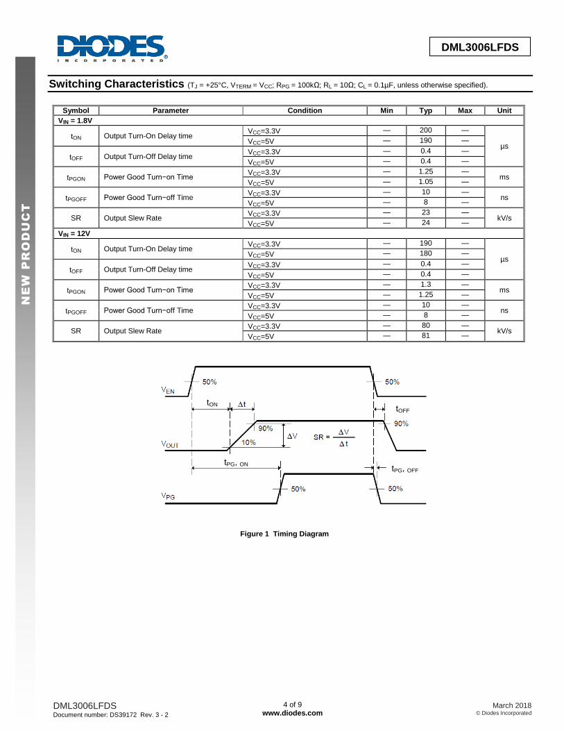
Switching Characteristics (TJ = +25°C, VTERM = VCC; RPG = 100kΩ; RL = 10Ω; CL = 0.1µF, unless otherwise specified).
Symbol Parameter Condition Min Typ Max Unit
VIN = 1.8V
tON Output Turn-On Delay time VCC=3.3V — 200 —
µs VCC=5V — 190 —
tOFF Output Turn-Off Delay time VCC=3.3V — 0.4 —
VCC=5V — 0.4 —
tPGON Power Good Turn−on Time VCC=3.3V — 1.25 —
ms VCC=5V — 1.05 —
tPGOFF Power Good Turn−off Time VCC=3.3V — 10 —
ns VCC=5V — 8 —
SR Output Slew Rate VCC=3.3V — 23 —
kV/s VCC=5V — 24 —
VIN = 12V
tON Output Turn-On Delay time VCC=3.3V — 190 —
µs VCC=5V — 180 —
tOFF Output Turn-Off Delay time VCC=3.3V — 0.4 —
VCC=5V — 0.4 —
tPGON Power Good Turn−on Time VCC=3.3V — 1.3 —
ms VCC=5V — 1.25 —
tPGOFF Power Good Turn−off Time VCC=3.3V — 10 —
ns VCC=5V — 8 —
SR Output Slew Rate VCC=3.3V — 80 —
kV/s VCC=5V — 81 —
tON
tPG, ONtPG, OFF
tOFF
Figure 1 Timing Diagram
DML3006LFDS Document number: DS39172 Rev. 3 - 2
5 of 9 www.diodes.com
March 2018 © Diodes Incorporated
DML3006LFDS
NE
W P
RO
DU
CT
AD
VA
NC
E IN
FO
RM
AT
IO
N
AD
VA
NC
ED
IN
FO
RM
AT
IO
N
NE
W P
RO
DU
CT
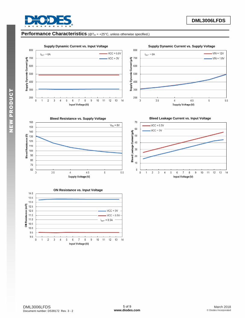
Performance Characteristics (@TA = +25°C, unless otherwise specified.)
Supply Dynamic Current vs. Input Voltage Supply Dynamic Current vs. Supply Voltage
Bleed Resistance vs. Supply Voltage Bleed Leakage Current vs. Input Voltage
ON Resistance vs. Input Voltage
DML3006LFDS Document number: DS39172 Rev. 3 - 2
6 of 9 www.diodes.com
March 2018 © Diodes Incorporated
DML3006LFDS
NE
W P
RO
DU
CT
AD
VA
NC
E IN
FO
RM
AT
IO
N
AD
VA
NC
ED
IN
FO
RM
AT
IO
N
NE
W P
RO
DU
CT
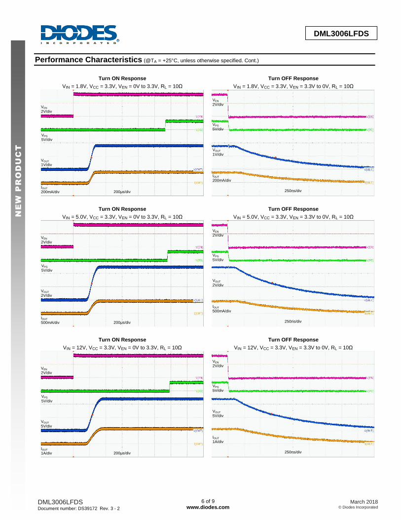
Performance Characteristics (@TA = +25°C, unless otherwise specified. Cont.)
Turn ON Response Turn OFF Response
VIN = 1.8V, VCC = 3.3V, VEN = 0V to 3.3V, RL = 10Ω
VIN = 1.8V, VCC = 3.3V, VEN = 3.3V to 0V, RL = 10Ω
Turn ON Response Turn OFF Response
VIN = 5.0V, VCC = 3.3V, VEN = 0V to 3.3V, RL = 10Ω
VIN = 5.0V, VCC = 3.3V, VEN = 3.3V to 0V, RL = 10Ω
Turn ON Response Turn OFF Response
VIN = 12V, VCC = 3.3V, VEN = 0V to 3.3V, RL = 10Ω
VIN = 12V, VCC = 3.3V, VEN = 3.3V to 0V, RL = 10Ω
200μs/div 250ns/div
VEN 2V/div
VPG 5V/div
VOUT 1V/div
IOUT 200mA/div
VEN 2V/div
VPG 5V/div
VOUT 1V/div
IOUT 200mA/div
200μs/div 250ns/div
VEN 2V/div
VPG 5V/div
VOUT 2V/div
IOUT 500mA/div
VEN 2V/div
VPG 5V/div
VOUT 2V/div
IOUT 500mA/div
200μs/div 250ns/div
VEN 2V/div
VPG 5V/div
VOUT 5V/div
IOUT 1A/div
VEN 2V/div
VPG 5V/div
VOUT 5V/div
IOUT 1A/div
DML3006LFDS Document number: DS39172 Rev. 3 - 2
7 of 9 www.diodes.com
March 2018 © Diodes Incorporated
DML3006LFDS
NE
W P
RO
DU
CT
AD
VA
NC
E IN
FO
RM
AT
IO
N
AD
VA
NC
ED
IN
FO
RM
AT
IO
N
NE
W P
RO
DU
CT
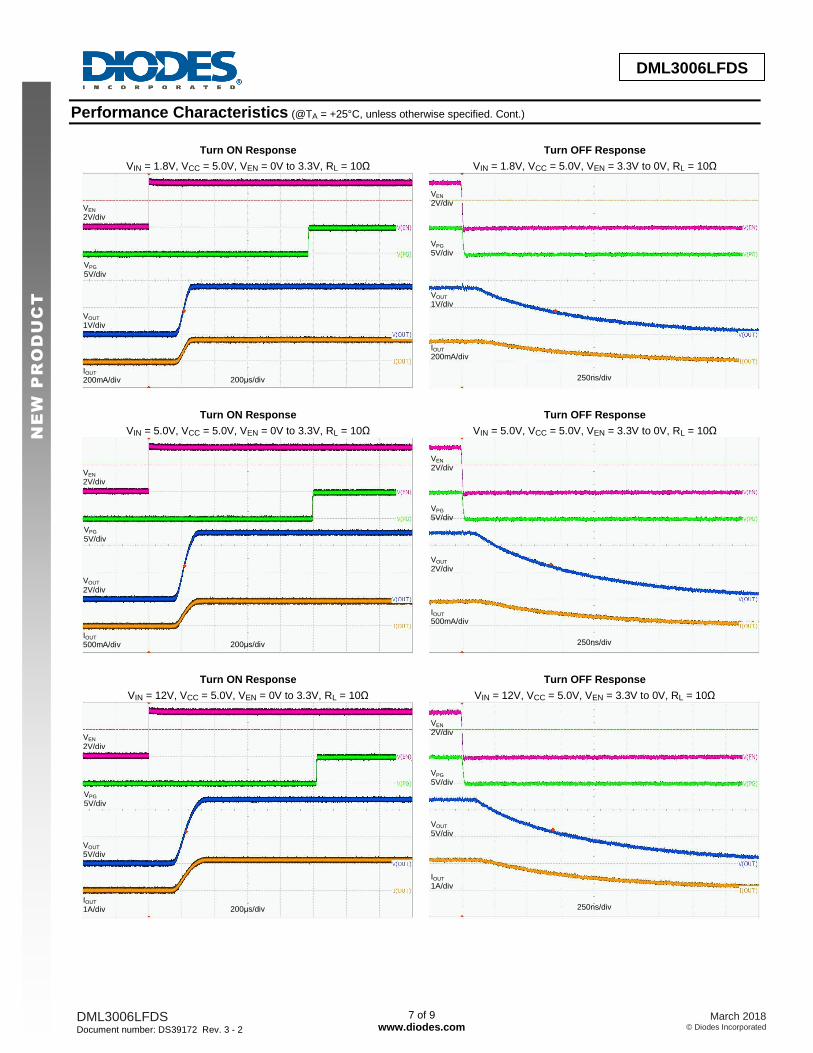
Performance Characteristics (@TA = +25°C, unless otherwise specified. Cont.)
Turn ON Response Turn OFF Response
VIN = 1.8V, VCC = 5.0V, VEN = 0V to 3.3V, RL = 10Ω
VIN = 1.8V, VCC = 5.0V, VEN = 3.3V to 0V, RL = 10Ω
Turn ON Response Turn OFF Response
VIN = 5.0V, VCC = 5.0V, VEN = 0V to 3.3V, RL = 10Ω
VIN = 5.0V, VCC = 5.0V, VEN = 3.3V to 0V, RL = 10Ω
Turn ON Response Turn OFF Response
VIN = 12V, VCC = 5.0V, VEN = 0V to 3.3V, RL = 10Ω
VIN = 12V, VCC = 5.0V, VEN = 3.3V to 0V, RL = 10Ω
200μs/div 250ns/div
VEN 2V/div
VPG 5V/div
VOUT 1V/div
IOUT 200mA/div
VEN 2V/div
VPG 5V/div
VOUT 1V/div
IOUT 200mA/div
200μs/div 250ns/div
VEN 2V/div
VPG 5V/div
VOUT 2V/div
IOUT 500mA/div
VEN 2V/div
VPG 5V/div
VOUT 2V/div
IOUT 500mA/div
200μs/div 250ns/div
VEN 2V/div
VPG 5V/div
VOUT 5V/div
IOUT 1A/div
VEN 2V/div
VPG 5V/div
VOUT 5V/div
IOUT 1A/div
DML3006LFDS Document number: DS39172 Rev. 3 - 2
8 of 9 www.diodes.com
March 2018 © Diodes Incorporated
DML3006LFDS
NE
W P
RO
DU
CT
AD
VA
NC
E IN
FO
RM
AT
IO
N
AD
VA
NC
ED
IN
FO
RM
AT
IO
N
NE
W P
RO
DU
CT
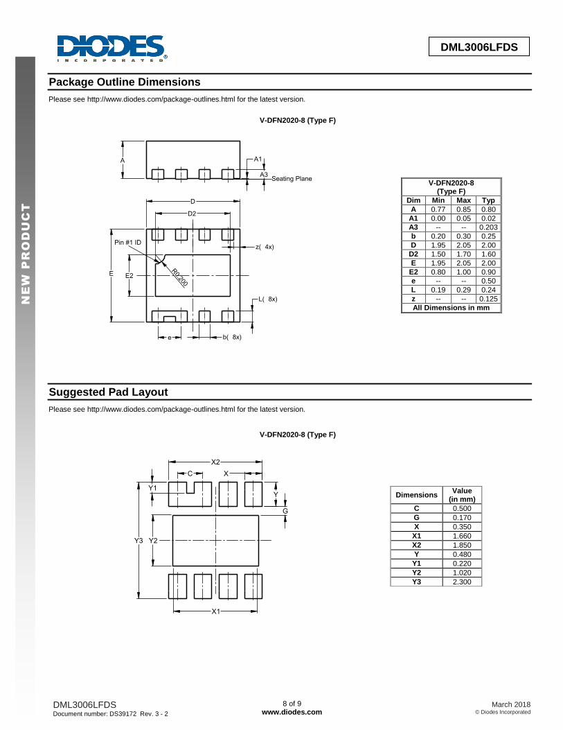
Package Outline Dimensions Please see http://www.diodes.com/package-outlines.html for the latest version.
V-DFN2020-8 (Type F)
D
D2
E
e b(8x)
L(8x)
E2
Pin #1 ID
R0.200
z(4x)
A3Seating Plane
A1A
V-DFN2020-8 (Type F)
Dim Min Max Typ
A 0.77 0.85 0.80
A1 0.00 0.05 0.02
A3 -- -- 0.203
b 0.20 0.30 0.25
D 1.95 2.05 2.00
D2 1.50 1.70 1.60
E 1.95 2.05 2.00
E2 0.80 1.00 0.90
e -- -- 0.50
L 0.19 0.29 0.24
z -- -- 0.125
All Dimensions in mm
Suggested Pad Layout Please see http://www.diodes.com/package-outlines.html for the latest version.
V-DFN2020-8 (Type F)
Y3
X2
C
Y2
X1
X
Y
G
Y1
Dimensions Value
(in mm)
C 0.500
G 0.170
X 0.350
X1 1.660
X2 1.850
Y 0.480
Y1 0.220
Y2 1.020
Y3 2.300
DML3006LFDS Document number: DS39172 Rev. 3 - 2
9 of 9 www.diodes.com
March 2018 © Diodes Incorporated
DML3006LFDS
NE
W P
RO
DU
CT
AD
VA
NC
E IN
FO
RM
AT
IO
N
AD
VA
NC
ED
IN
FO
RM
AT
IO
N
NE
W P
RO
DU
CT
IMPORTANT NOTICE DIODES INCORPORATED MAKES NO WARRANTY OF ANY KIND, EXPRESS OR IMPLIED, WITH REGARDS TO THIS DOCUMENT, INCLUDING, BUT NOT LIMITED TO, THE IMPLIED WARRANTIES OF MERCHANTABILITY AND FITNESS FOR A PARTICULAR PURPOSE (AND THEIR EQUIVALENTS UNDER THE LAWS OF ANY JURISDICTION). Diodes Incorporated and its subsidiaries reserve the right to make modifications, enhancements, improvements, corrections or other changes without further notice to this document and any product described herein. Diodes Incorporated does not assume any liability arising out of the application or use of this document or any product described herein; neither does Diodes Incorporated convey any license under its patent or trademark rights, nor the rights of others. Any Customer or user of this document or products described herein in such applications shall assume all risks of such use and will agree to hold Diodes Incorporated and all the companies whose products are represented on Diodes Incorporated website, harmless against all damages. Diodes Incorporated does not warrant or accept any liability whatsoever in respect of any products purchased through unauthorized sales channel. Should Customers purchase or use Diodes Incorporated products for any unintended or unauthorized application, Customers shall indemnify and hold Diodes Incorporated and its representatives harmless against all claims, damages, expenses, and attorney fees arising out of, directly or indirectly, any claim of personal injury or death associated with such unintended or unauthorized application. Products described herein may be covered by one or more United States, international or foreign patents pending. Product names and markings noted herein may also be covered by one or more United States, international or foreign trademarks. This document is written in English but may be translated into multiple languages for reference. Only the English version of this document is the final and determinative format released by Diodes Incorporated.
LIFE SUPPORT Diodes Incorporated products are specifically not authorized for use as critical components in life support devices or systems without the express written approval of the Chief Executive Officer of Diodes Incorporated. As used herein: A. Life support devices or systems are devices or systems which: 1. are intended to implant into the body, or
2. support or sustain life and whose failure to perform when properly used in accordance with instructions for use provided in the labeling can be reasonably expected to result in significant injury to the user.
B. A critical component is any component in a life support device or system whose failure to perform can be reasonably expected to cause the failure of the life support device or to affect its safety or effectiveness. Customers represent that they have all necessary expertise in the safety and regulatory ramifications of their life support devices or systems, and acknowledge and agree that they are solely responsible for all legal, regulatory and safety-related requirements concerning their products and any use of Diodes Incorporated products in such safety-critical, life support devices or systems, notwithstanding any devices- or systems-related information or support that may be provided by Diodes Incorporated. Further, Customers must fully indemnify Diodes Incorporated and its representatives against any damages arising out of the use of Diodes Incorporated products in such safety-critical, life support devices or systems. Copyright © 2018, Diodes Incorporated www.diodes.com