Embed Size (px)
Citation preview

PAM8012 Document number: DSxxxxx Rev. 1 - 3
1 of 14 www.diodes.com
October 2012© Diodes Incorporated
PAM8012
A Product Line ofDiodes Incorporated
MONO 2.0W ANTI-SATURATION CLASS-D AUDIO POWER AMPLIFIER with POWER LIMIT
Description The PAM8012 is a 2.0W mono filterless class-D amplifier with high PSRR and differential input that reduce noise. Features like 90% efficiency and small PCB area make the PAM8012 Class-D amplifier ideal for cellular handsets. The filterless architecturerequires no external output filter, fewer external components, less PCB area and lower system costs, and simplifies application design. The PAM8012 features anti-saturation function which detect output signal clip due to the over input level and keep the output non-saturation automatically to get the excellent sound quality. The maximum output power without clip can be set by one resistor at PL pin that to prevent the speaker to be damaged. The PAM8012 features short circuit protection and over temperature protection. The PAM8012 is available in tiny WCSP9 (1.3mm x 1.3mm) and eMSOP10 packages.
Features • 1.0W/2.0W @ <1% THD Output with a 8Ω/ 4Ω Load at 5V
Supply • Maximum Output Power Can Be Set by One External Resistor • Minimized ON/OFF Pop Noise • Superior Low Noise • High PSRR • Supply Voltage from 2.5V to 5.5V • Auto Recovering Short Circuit Protection • Over Temperature Protection • 9 Ball, 1.3mm x 1.3mm, 0.4mm Pitch WCSP and eMSOP10
Packages
Applications • Wireless or Cellular Handsets and PDAs • Portable Navigation Devices • General Portable Audio Devices
Pin Assignments
参考資料

PAM8012 Document number: DSxxxxx Rev. 1 - 3
2 of 14 www.diodes.com
October 2012© Diodes Incorporated
PAM8012
A Product Line ofDiodes Incorporated
Typical Applications Circuit
Functional Block Diagram
参考資料
PAM8012 Document number: DSxxxxx Rev. 1 - 3
3 of 14 www.diodes.com
October 2012© Diodes Incorporated
PAM8012
A Product Line ofDiodes Incorporated
Absolute Maximum Ratings (@TA = +25°C, unless otherwise specified.) These are stress ratings only and functional operation is not implied. Exposure to absolute maximum ratings for prolonged time periods may affect device reliability. All voltages are with respect to ground.
Parameter Rating Unit Supply Voltage, VDD 6.0
V Input Voltage, IN+, IN- -0.3 to VDD +0.3 Minimum Load Resistance 3.2 Ω Maximum Junction Temperature -65 to +150
°C Storage Temperature 150 Soldering Temperature 260, 10sec
Recommended Operating Conditions (@TA = +25°C, unless otherwise specified.)
Parameter Rating Unit Supply Voltage Range 2.5 to 5.5 V Ambient Temperature Range -40 to +85
°C Junction Temperature Range -40 to +125
Thermal Information
Parameter Package Symbol Max Unit
Thermal Resistance (Junction to Ambient) WCSP9 1.3 x 1.3
θJA 100
°C/W eMSOP10 60
Thermal Resistance (Junction to Case) WCSP9 1.3 x 1.3
θJC 40
eMSOP10 30
参考資料

PAM8012 Document number: DSxxxxx Rev. 1 - 3
4 of 14 www.diodes.com
October 2012© Diodes Incorporated
PAM8012
A Product Line ofDiodes Incorporated
Electrical Characteristics (@TA = +25°C, VDD = 5V, unless otherwise specified.)
Symbol Parameter Test Conditions Min Typ Max UnitsVDD Supply Voltage 2.5 5.5 V
PO Output Power RPL = 110KΩ, f = 3kHz, R = 4Ω VDD = 5V 2.0 W RPL = 110KΩ, f = 3kHz, R = 8Ω VDD = 5V 1.0
THD+N Total Harmonic Distortion Plus Noise
VDD = 5V, PO = 1W, R = 4Ω f = 1kHz
0.08 VDD = 3.6V, PO = 2W, R = 4Ω 0.08 % VDD = 5V, PO = 1W, R = 8Ω
f = 1kHz 0.08
VDD = 5V, PO = 0.5W, R = 8Ω 0.08 %
PSRR AC Power Supply Ripple Rejection f = 217Hz, Inputs AC-Grounded with CIN = 0.1µF
VDD = 5.0V -75 VDD = 3.6V -75
SNR Signal to Noise Ratio THD = 1%, f = 1KHz VDD = 5.0V 95 dB VDD = 3.6V 95
VN Output Noise CIN = 0.1µF, Inputs AC-Grounded No A-Weighting 60 A-Weighting 40 µV
η Peak Efficiency RL = 8Ω f = 1kHz 90 RL = 4Ω 87 %
IQ Quiescent Current VEN = 5.0V, VDD = 5V, PL = 0V No Load 4.2 mA ISD Shutdown Current VDD = 2.5V to 5.5V, VEN = 0V No Load 1 µA
|VOS| Offdet Voltage VDD = 5V -20 +20 mV RIN Input Resistor VDD = 5V 31 KΩ GV Closed Loop Gain VDD = 5V 18 dB fSW Switching Frequency VDD = 5V 250 KHz TON Turn-On Time VDD = 5V 45 mS OTP Over Temperature Protection VDD = 5V No Load 150 °C OTH Over Temperature Hysterisis VDD = 5V No Load 40 °C VENH High-Level EN Voltage VDD = 5V 1.4 V VENL Low-Level EN Voltage VDD = 5V 0.4 V AR Maximum Attenuation Range Anti-Saturation Active from +18dB to -18dB 26 dB
参考資料

PAM8012 Document number: DSxxxxx Rev. 1 - 3
5 of 14 www.diodes.com
October 2012© Diodes Incorporated
PAM8012
A Product Line ofDiodes Incorporated
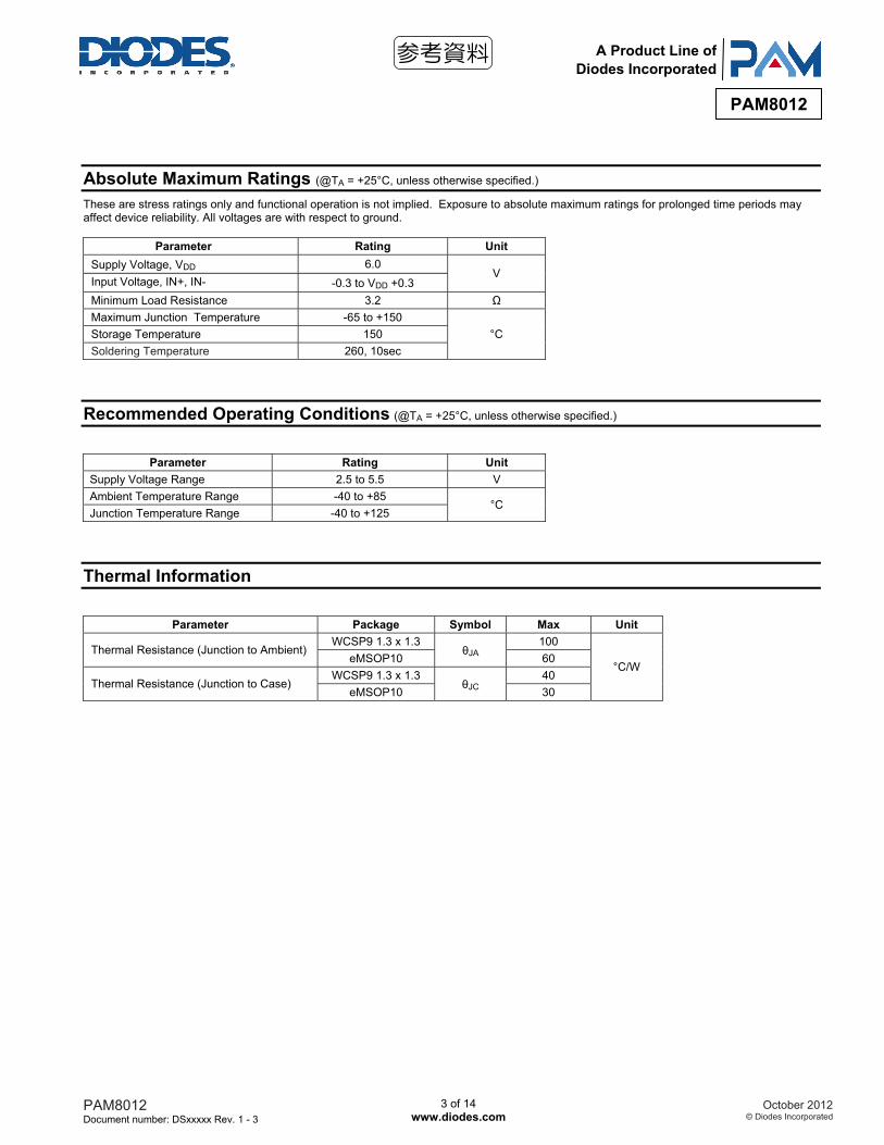
Typical Performance Characteristics (@TA = +25°C, VDD = 5V, unless otherwise specified.)
参考資料
PAM8012 Document number: DSxxxxx Rev. 1 - 3
6 of 14 www.diodes.com
October 2012© Diodes Incorporated
PAM8012
A Product Line ofDiodes Incorporated
Typical Performance Characteristics (cont.) (@TA = +25°C, VDD = 5V, unless otherwise specified.)
参考資料

PAM8012 Document number: DSxxxxx Rev. 1 - 3
7 of 14 www.diodes.com
October 2012© Diodes Incorporated
PAM8012
A Product Line ofDiodes Incorporated
Application Information
Test Setup for Performance Testing
Notes: 1. The AP AUX-0025 low pass filter is necessary for class-D amplifier measurement with AP analyzer. 2. Two 33μH inductors are used in series with load resistor to emulate the small speaker for efficiency measurement. Anti-Saturation The Anti-saturation feature provides continuous automatic gain adjustment to the amplifier through an internal circuit. This feature enhances the perceived audio loudness and at the same time prevents speaker damage from occurring. The Anti-saturation works by detecting the output. The gain changes depending on the supply voltage, and the attack and release time. The gain changes constantly as the audio signal increases and/or decreases. The gain step size for the Anti-saturation is 0.4 dB. If the audio signal has near-constant amplitude, the gain does not change. Table 1 shows the Anti-saturation variable description. Table 1. PAM8012 Anti-Saturation Variable Description
Varible Description Value
Gain The pre-set gain of the device when the Anit-saturation is inactive. The fixed gain is also the initial gain when the device comes out of shutdown mode or when the Anti-saturation is disabled.
18dB (Maximum)
Attack Time The minimum time between two gain decrements. 128µS Release Time The minimum time between two gain increments. 256mS
PL Terminal Function The voltage value of PL sets the PAM8012 maximum output by an external resistor. Refer to table 2 for anti-saturation and power limit selection. Table 2. PAM8012 Anti-Saturation and Power Limit Variable Description
RPL 0 30K < RPL < 120K Open
EN VDD PL: OFF
Anti-Sat: OFF PL: ON
Anti-Sat: ON PL: OFF
Anti-Sat: ON
VDD/2 PL: OFF Anti-Sat: OFF
PL: ON Anti-Sat: OFF
PL: ON Anti-Sat: OFF
参考資料

PAM8012 Document number: DSxxxxx Rev. 1 - 3
8 of 14 www.diodes.com
October 2012© Diodes Incorporated
PAM8012
A Product Line ofDiodes Incorporated
Application Information (cont.)
Input Capacitors (CI) In the typical application, an input capacitor, Ci, is required to allow the amplifier to bias the input signal to the proper DC level for optimum operation. In this case, Ci and the minimum input impedance RI form is a high-pass filter with the corner frequency determined in the follow equation:
CR2
1f
IIC Π=
It is important to consider the value of CI as it directly affects the low frequency performance of the circuit. For example, the specification calls for a flat bass response are down to 150Hz. Equation is reconfigured as followed:
fR2
1C
III Π=
When input resistance variation is considered, the CI is 34nF, so one would likely choose a value of 33nF. A further consideration for this capacitor is the leakage path from the input source through the input network (CI, RI + RF) to the load. This leakage current creates a DC offset voltage at the input to the amplifier that reduces useful headroom, especially in high gain applications. For this reason, a low-leakage tantalum or ceramic capacitor is the best choice. When polarized capacitors are used, the positive side of the capacitor should face the amplifier input in most applications as the DC level is held at VDD/2, which is likely higher than the source DC level. Please note that it is important to confirm the capacitor polarity in the application. Decoupling Capacitor (CS) The PAM8012 is a high-performance CMOS audio amplifier that requires adequate power supply decoupling to ensure the output total harmonic distortion (THD) as low as possible. Power supply decoupling also prevents the oscillations causing by long lead length between the amplifier and the speaker. The optimum decoupling is achieved by using two different types of capacitors that target on different types of noise on the power supply leads. For higher frequency transients, spikes, or digital hash on the line, a good low equivalentseries- resistance (ESR) ceramic capacitor, typically 1µF, is placed as close as possible to VDD pin for the best operation. For filtering lower frequency noise signals, a large ceramic capacitor of 10µF or greater placed near the audio power amplifier is recommended. How to Reduce EMI Most applications require a ferrite bead filter for EMI elimination shown at Figure 1. The ferrite filter reduces EMI around 1MHz and higher. When selecting a ferrite bead, choose one with high impedance at high frequencies, but low impedance at low frequencies.
Figure 1: Ferrite Bead Filter to Reduce EMI Shutdown Operation In order to reduce power consumption while not in use, the PAM8012 contains shutdown circuitry that is used to turn off the amplifier’s bias circuitry. This shutdown feature turns the amplifier off when logic low is placed on the EN pin. By switching the EN pin connected to GND, the PAM8012 supply current draw will be minimized in idle mode. Short Circuit Protection (SCP) The PAM8012 has short circuit protection circuitry on the outputs to prevent the device from damage when output-to-output shorts or output-to-GND shorts occur. When a short circuit occurs, the device immediately goes into shutdown state. Once the short is removed, the device will be reactivated.
参考資料

PAM8012 Document number: DSxxxxx Rev. 1 - 3
9 of 14 www.diodes.com
October 2012© Diodes Incorporated
PAM8012
A Product Line ofDiodes Incorporated
Application Information (cont.)
Over Temperature Protection (OTP) Thermal protection on the PAM8012 prevents the device from damage when the internal die temperature exceeds +150°C. There is a +15°C tolerance on this trip point from device to device. Once the die temperature exceeds the set point, the device will enter the shutdown state and the outputs are disabled. This is not a latched fault. The thermal fault is cleared once the temperature of the die decreased by +40°C. This large hysteresis will prevent motor boating sound well and the device begins normal operation at this point with no external system interaction. POP and Click Circuitry The PAM8012 contains circuitry to minimize turnon and turn-off transients or “click and pops”, where turn-on refers to either power supply turn-on or device recover from shutdown mode. When the device is turned on, the amplifiers are internally muted. An internal current source ramps up the reference voltage. The device will remain in mute mode until the reference voltage reach half supply voltage, ½ VDD. As soon as the reference voltage is stable the device will begin full operation. For the best power-off pop performance, the amplifier should be set in shutdown mode prior to removing the power supply voltage. PCB Layout Guidelines Grounding It is recommended to use plane grounding. Noise currents in the output power stage need to be returned to output noise ground and nowhere else. When these currents circulate elsewhere, they may get into the power supply, or the signal ground, etc, even worse, they may form a loop and radiate noise. Any of these instances results in degraded amplifier performance. The output noise ground that the logical returns for the output noise currents with Class-D switching must tie to system ground at the power exclusively. Signal currents for the inputs, reference need to be returned to quite ground. This ground only ties to the signal components and the GND pin. GND then ties to system ground. Power Supply Line It is recommended that all the trace could be routed as short and thick as possible. For the power line layout, just imagine water stream, any barricade placed in the trace (shown in Figure 2) could result in the bad performance of the amplifier.
Figure 2: Power Line
Components Placement Decoupling capacitors as previously described, the high-frequency 1µF decoupling capacitors should be placed as close to the power supply terminals VDD as possible. Large bulk power supply decoupling capacitors (10µF or greater) should be placed near the PAM8012 on the VDD terminal. Input resistors and capacitors need to be placed very close to input pins. Output filter - The ferrite EMI filter should be placed as close to the output terminals as possible for the best EMI performance, and the capacitors used in the filters should be grounded to system ground.
参考資料

PAM8012 Document number: DSxxxxx Rev. 1 - 3
10 of 14 www.diodes.com
October 2012© Diodes Incorporated
PAM8012
A Product Line ofDiodes Incorporated
Ordering Information
Part Number Part Marking Package Type Standard Package
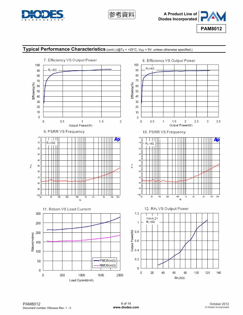
PAM8012AZN BI YW WCSP (1.3mm x 1.3mm) 3000 Units/Tape&Reel
PAM8012BSM P8012 XXXYW eMSOP10 2500 Units/Tape&Reel
参考資料
PAM8012 Document number: DSxxxxx Rev. 1 - 3
11 of 14 www.diodes.com
October 2012© Diodes Incorporated
PAM8012
A Product Line ofDiodes Incorporated
Marking Information
参考資料

PAM8012 Document number: DSxxxxx Rev. 1 - 3
12 of 14 www.diodes.com
October 2012© Diodes Incorporated
PAM8012
A Product Line ofDiodes Incorporated
Package Outline Dimensions (All dimensions in mm.) WCSP9
参考資料
PAM8012 Document number: DSxxxxx Rev. 1 - 3
13 of 14 www.diodes.com
October 2012© Diodes Incorporated
PAM8012
A Product Line ofDiodes Incorporated
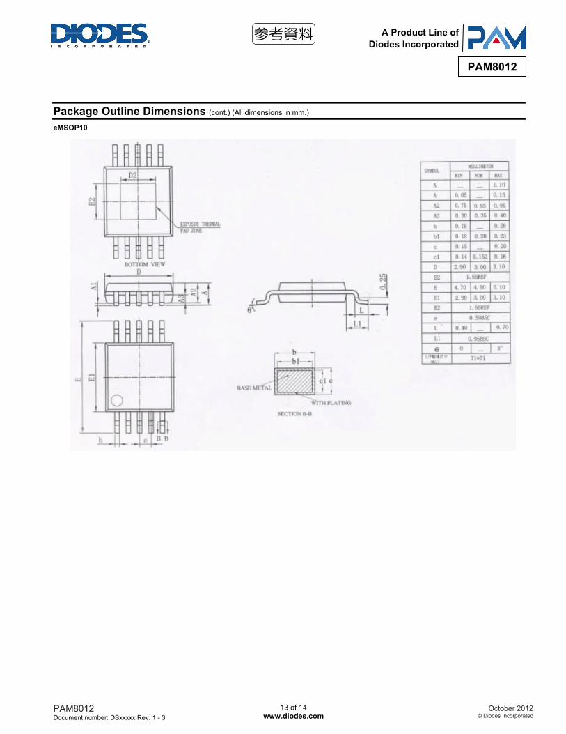
Package Outline Dimensions (cont.) (All dimensions in mm.) eMSOP10
参考資料