Embed Size (px)
Citation preview
PAM8303D Document number: DSxxxxx Rev. 1 - 7
1 of 16 www.diodes.com
November 2012© Diodes Incorporated
PAM8303D
A Product Line ofDiodes Incorporated
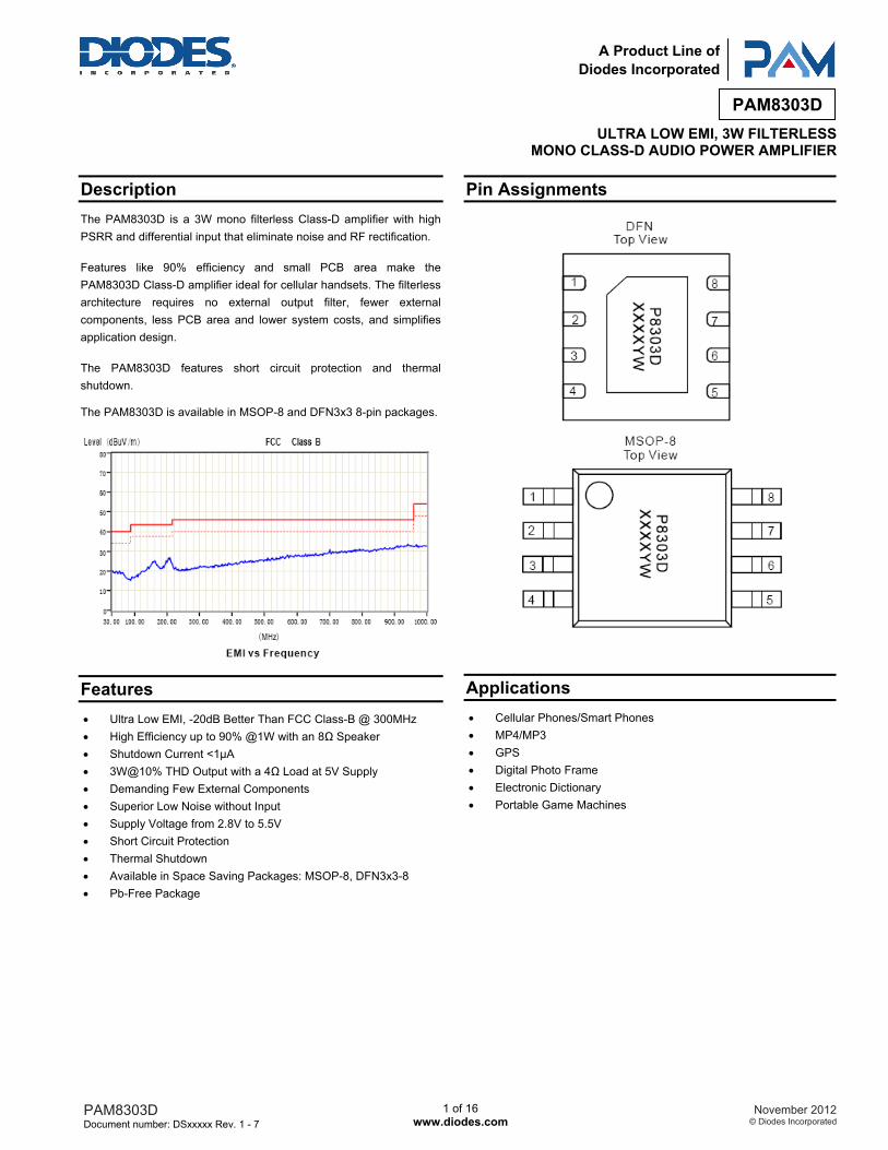
ULTRA LOW EMI, 3W FILTERLESS MONO CLASS-D AUDIO POWER AMPLIFIER
Description The PAM8303D is a 3W mono filterless Class-D amplifier with high PSRR and differential input that eliminate noise and RF rectification. Features like 90% efficiency and small PCB area make the PAM8303D Class-D amplifier ideal for cellular handsets. The filterless architecture requires no external output filter, fewer externalcomponents, less PCB area and lower system costs, and simplifies application design. The PAM8303D features short circuit protection and thermal shutdown. The PAM8303D is available in MSOP-8 and DFN3x3 8-pin packages.
Features • Ultra Low EMI, -20dB Better Than FCC Class-B @ 300MHz • High Efficiency up to 90% @1W with an 8Ω Speaker • Shutdown Current <1µA • 3W@10% THD Output with a 4Ω Load at 5V Supply • Demanding Few External Components • Superior Low Noise without Input • Supply Voltage from 2.8V to 5.5V • Short Circuit Protection • Thermal Shutdown • Available in Space Saving Packages: MSOP-8, DFN3x3-8 • Pb-Free Package
Pin Assignments
Applications • Cellular Phones/Smart Phones • MP4/MP3 • GPS • Digital Photo Frame • Electronic Dictionary • Portable Game Machines
PAM8303D Document number: DSxxxxx Rev. 1 - 7
2 of 16 www.diodes.com
November 2012© Diodes Incorporated
PAM8303D
A Product Line ofDiodes Incorporated
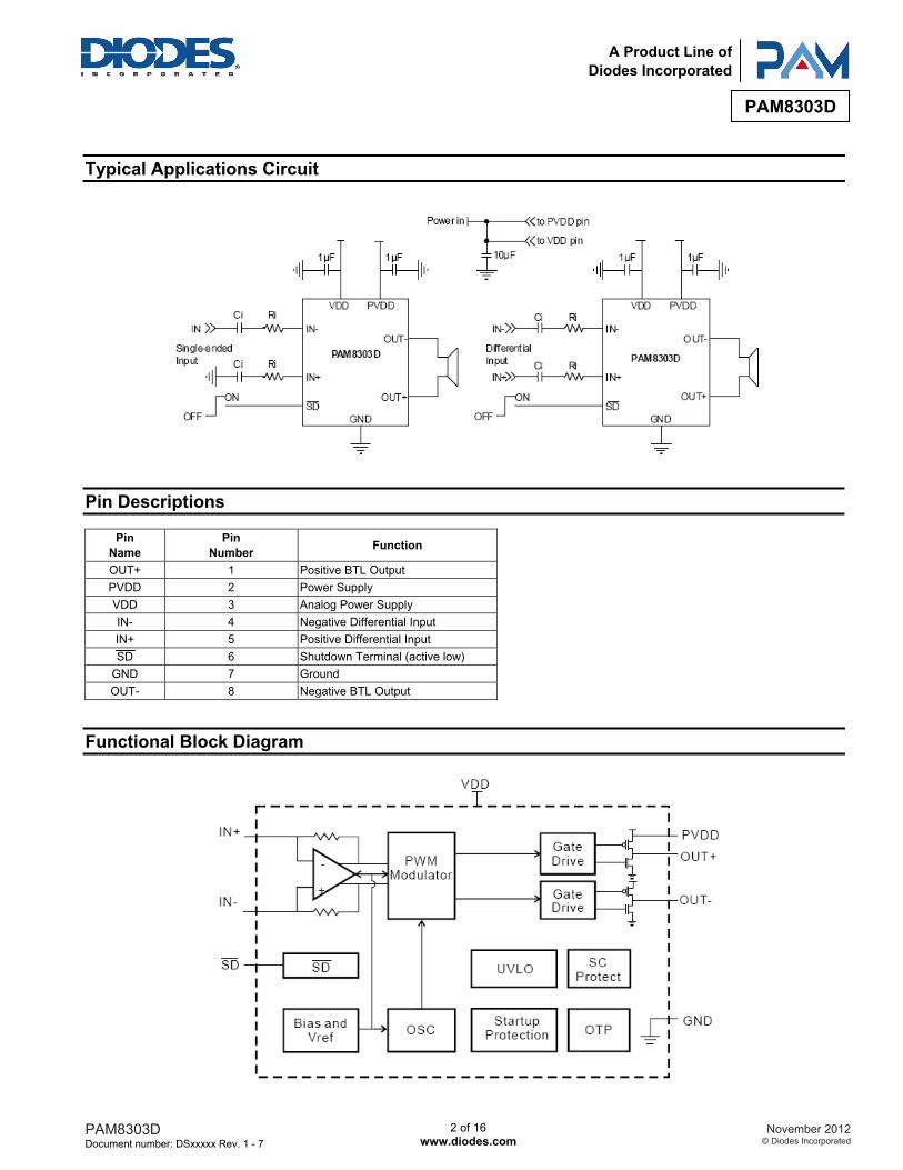
Typical Applications Circuit
Pin Descriptions
Pin Name
Pin Number Function
OUT+ 1 Positive BTL Output PVDD 2 Power Supply VDD 3 Analog Power Supply IN- 4 Negative Differential Input IN+ 5 Positive Differential Input SD 6 Shutdown Terminal (active low)
GND 7 Ground OUT- 8 Negative BTL Output
Functional Block Diagram

PAM8303D Document number: DSxxxxx Rev. 1 - 7
3 of 16 www.diodes.com
November 2012© Diodes Incorporated
PAM8303D
A Product Line ofDiodes Incorporated
Absolute Maximum Ratings (@TA = +25°C, unless otherwise specified.) These are stress ratings only and functional operation is not implied. Exposure to absolute maximum ratings for prolonged time periods may affect device reliability. All voltages are with respect to ground.
Parameter Rating Unit Supply Voltage 6.0
V Input Voltage -0.3 to VDD +0.3 Maximum Junction Temperature 150
°C Storage Temperature -65 to +150 Soldering Temperature 250, 10 sec
Recommended Operating Conditions (@TA = +25°C, unless otherwise specified.)
Parameter Rating Unit Supply Voltage Range 2.8 to 5.5 V Ambient Temperature Range -40 to +85 °C Junction Temperature Range -40 to +125 °C
Thermal Information
Parameter Package Symbol Max Unit
Thermal Resistance (Junction to Ambient) MSOP-8
θJA 180
°C/W DFN3x3-8 47.9 Thermal Resistance (Junction to Case) MSOP-8 θJC 75

PAM8303D Document number: DSxxxxx Rev. 1 - 7
4 of 16 www.diodes.com
November 2012© Diodes Incorporated
PAM8303D
A Product Line ofDiodes Incorporated
Electrical Characteristics (@TA = +25°C, VDD = 5V, Gain = 2V/V, RL = L(33µH) + R + L(33µH), unless otherwise specified.)
Symbol Parameter Test Conditions Min Typ Max Units VDD Supply Voltage 2.8 5.5 V
PO Output Power
THD+N = 10%, f = 1KHz, R = 4Ω VDD = 5.0V 2.85 3.00
W VDD = 3.6V 1.65 1.80 VDD = 3.2V 1.20 1.35
THD+N = 1%, f = 1KHz, R = 4Ω VDD = 5.0V 2.50 2.66
W VDD = 3.6V 1.15 1.30 VDD = 3.2V 0.85 1.0
THD+N = 10%, f = 1KHz, R = 8Ω VDD = 5.0V 1.65 1.80
W VDD = 3.6V 0.75 0.90 VDD = 3.2V 0.55 0.70
THD+N = 1%, f = 1KHz, R = 8Ω VDD = 5.0V 1.3 1.5
W VDD = 3.6V 0.55 0.72 VDD = 3.2V 0.40 0.55
THD+N Total Harmonic Distortion Plus Noise
VDD = 5.0V, PO = 1W, R = 8Ω f = 1kHz
0.28 0.35 % VDD = 3.6V, PO = 0.1W, R = 8Ω 0.40 0.45
VDD = 3.2V, PO = 0.1W, R = 8Ω 0.55 0.60 VDD = 5.0V, PO = 0.5W, R = 4Ω
f = 1kHz 0.20 0.25
% VDD = 3.6V, PO = 0.2W, R = 4Ω 0.35 0.40 VDD = 3.2V, PO = 0.1W, R = 4Ω 0.5 0.55
PSRR Power Supply Ripple Rejection VDD = 3.6V, Inputs AC-Grounded with CIN = 1µF
f = 217Hz -63 -55
dB f = 1kHz -62 -55 f = 10kHz -52 -40
Dyn Dynamic Range VDD = 5V, THD = 1%, R = 8Ω f = 1kHz 85 95
VN Output Noise Inputs AC-Grounded No A-Weighting 50 100
µV A-Weighting 30 60
CMRR Common Mode Rejection Ratio VIC = 100m, VPP, f =1kHz 40 63 dB
η Peak Efficiency RL = 8Ω, THD = 10%
f = 1kHz 85 90
RL = 4Ω, THD = 10% 80 86 %
IQ Quiescent Current VDD = 5.0V
R = 8Ω 7.5 10
VDD = 3.6V 4.6 7.0 VDD = 3.0V 3.6 5.0 mA
ISD Shutdown Current VDD = 3.0V to 5.0V VSD = 0.3V 0.5 2.0 µA
RDS(ON) Static Drain-to-Source On-State Resistor
CSP Package, High Side PMOS plus Low Side NMOS, I = 500mA
VDD = 5.0V 280 350 VDD = 3.6V 300 375 VDD = 3.0V 325 400
MSOP/DFN package, High Side PMOS plus Low Side NMOS, I = 500mA
VDD = 5.0V 365 420 VDD = 3.6V 385 450 VDD = 3.0V 410 500
RIN Input Resistance 150 KΩ fSW Switching Frequency VDD = 3V to 5V 200 250 300 KHz GV Closed Loop Gain VDD = 3V to 5V 300kΩ/RI dB VOS Output Offset Voltage Input AC-Ground, VDD = 5V 10 50 mV VIH Enable Input High Voltage VDD = 5V 1.5 V VIL Enable Input Low Voltage VDD = 5V 0.3 V
PAM8303D Document number: DSxxxxx Rev. 1 - 7
5 of 16 www.diodes.com
November 2012© Diodes Incorporated
PAM8303D
A Product Line ofDiodes Incorporated
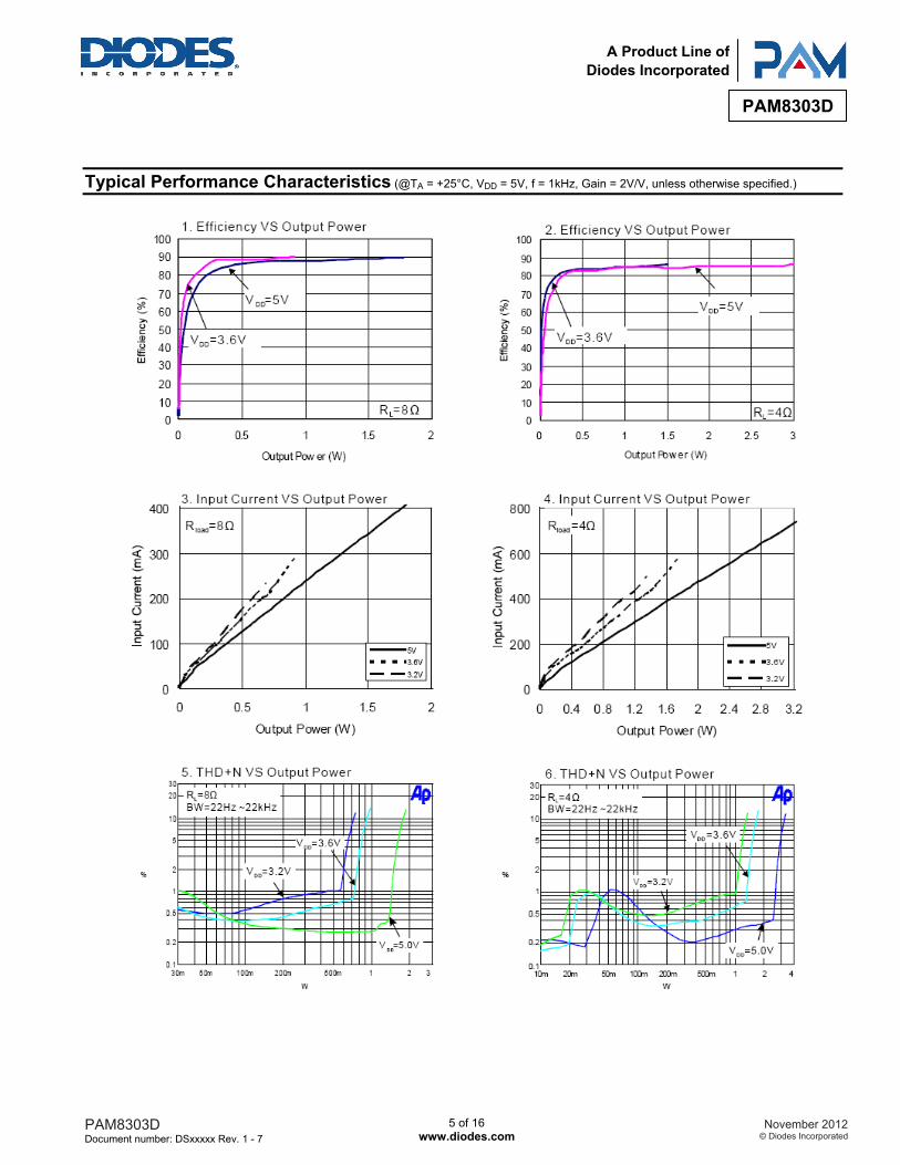
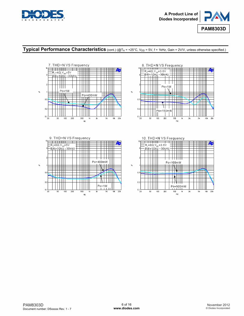
Typical Performance Characteristics (@TA = +25°C, VDD = 5V, f = 1kHz, Gain = 2V/V, unless otherwise specified.)
PAM8303D Document number: DSxxxxx Rev. 1 - 7
6 of 16 www.diodes.com
November 2012© Diodes Incorporated
PAM8303D
A Product Line ofDiodes Incorporated
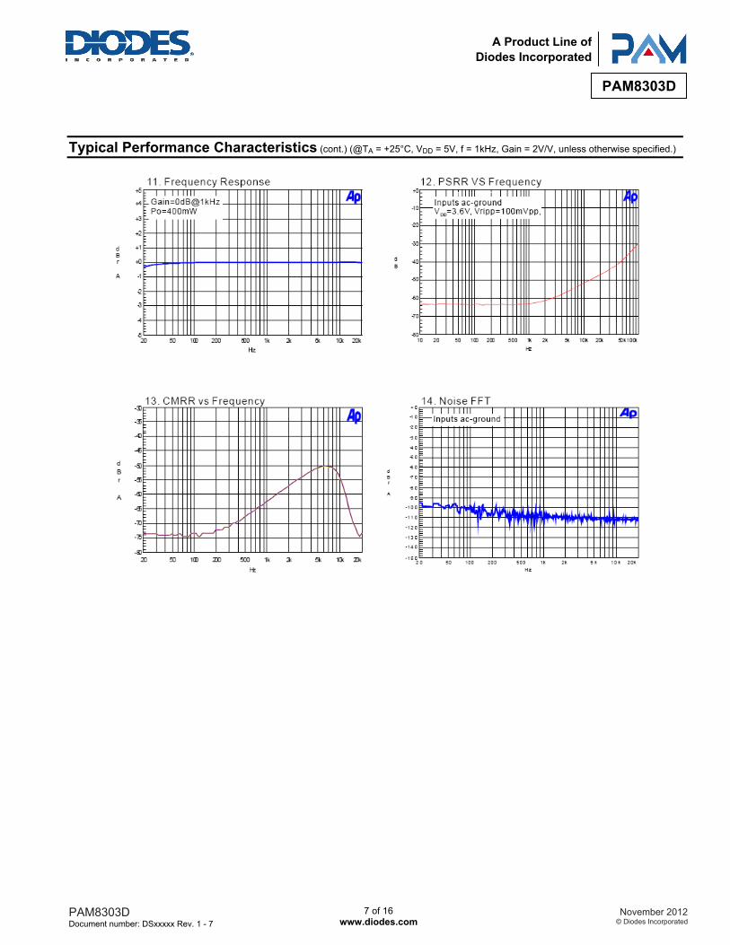
Typical Performance Characteristics (cont.) (@TA = +25°C, VDD = 5V, f = 1kHz, Gain = 2V/V, unless otherwise specified.)
PAM8303D Document number: DSxxxxx Rev. 1 - 7
7 of 16 www.diodes.com
November 2012© Diodes Incorporated
PAM8303D
A Product Line ofDiodes Incorporated
Typical Performance Characteristics (cont.) (@TA = +25°C, VDD = 5V, f = 1kHz, Gain = 2V/V, unless otherwise specified.)

PAM8303D Document number: DSxxxxx Rev. 1 - 7
8 of 16 www.diodes.com
November 2012© Diodes Incorporated
PAM8303D
A Product Line ofDiodes Incorporated
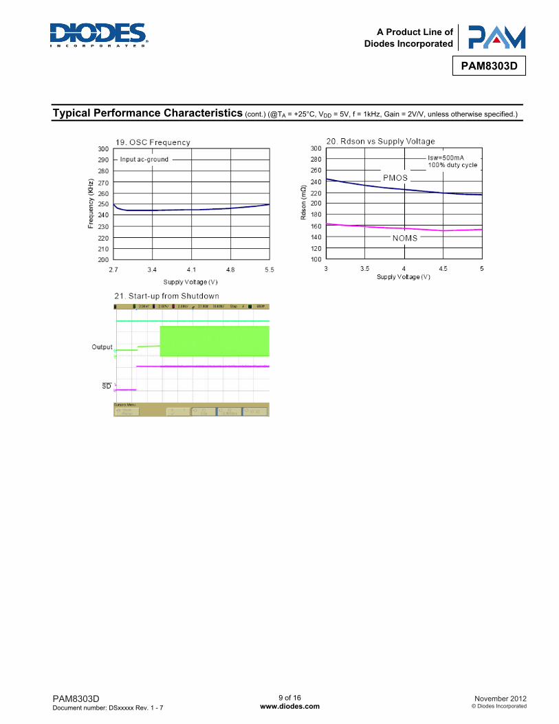
Typical Performance Characteristics (cont.) (@TA = +25°C, VDD = 5V, f = 1kHz, Gain = 2V/V, unless otherwise specified.)
PAM8303D Document number: DSxxxxx Rev. 1 - 7
9 of 16 www.diodes.com
November 2012© Diodes Incorporated
PAM8303D
A Product Line ofDiodes Incorporated
Typical Performance Characteristics (cont.) (@TA = +25°C, VDD = 5V, f = 1kHz, Gain = 2V/V, unless otherwise specified.)
PAM8303D Document number: DSxxxxx Rev. 1 - 7
10 of 16 www.diodes.com
November 2012© Diodes Incorporated
PAM8303D
A Product Line ofDiodes Incorporated
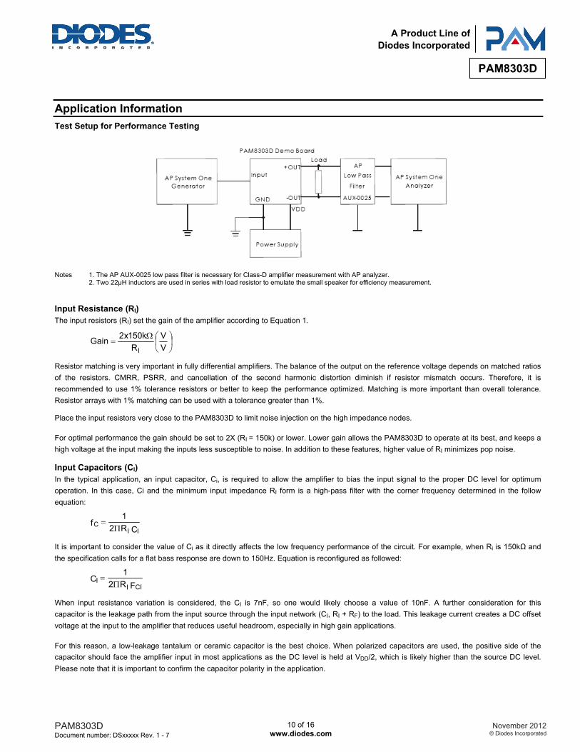
Application Information
Test Setup for Performance Testing
Notes 1. The AP AUX-0025 low pass filter is necessary for Class-D amplifier measurement with AP analyzer. 2. Two 22μH inductors are used in series with load resistor to emulate the small speaker for efficiency measurement. Input Resistance (RI) The input resistors (RI) set the gain of the amplifier according to Equation 1.
⎟⎠
⎞⎜⎝
⎛Ω=
VV
Rk150x2Gain
I
Resistor matching is very important in fully differential amplifiers. The balance of the output on the reference voltage depends on matched ratios of the resistors. CMRR, PSRR, and cancellation of the second harmonic distortion diminish if resistor mismatch occurs. Therefore, it is recommended to use 1% tolerance resistors or better to keep the performance optimized. Matching is more important than overall tolerance. Resistor arrays with 1% matching can be used with a tolerance greater than 1%. Place the input resistors very close to the PAM8303D to limit noise injection on the high impedance nodes. For optimal performance the gain should be set to 2X (RI = 150k) or lower. Lower gain allows the PAM8303D to operate at its best, and keeps a high voltage at the input making the inputs less susceptible to noise. In addition to these features, higher value of RI minimizes pop noise. Input Capacitors (CI) In the typical application, an input capacitor, Ci, is required to allow the amplifier to bias the input signal to the proper DC level for optimum operation. In this case, Ci and the minimum input impedance RI form is a high-pass filter with the corner frequency determined in the follow equation:
CR2
1f
IIC Π=
It is important to consider the value of Ci as it directly affects the low frequency performance of the circuit. For example, when Ri is 150kΩ and the specification calls for a flat bass response are down to 150Hz. Equation is reconfigured as followed:
FR2
1C
CIII Π=
When input resistance variation is considered, the CI is 7nF, so one would likely choose a value of 10nF. A further consideration for this capacitor is the leakage path from the input source through the input network (CI, RI + RF) to the load. This leakage current creates a DC offset voltage at the input to the amplifier that reduces useful headroom, especially in high gain applications. For this reason, a low-leakage tantalum or ceramic capacitor is the best choice. When polarized capacitors are used, the positive side of the capacitor should face the amplifier input in most applications as the DC level is held at VDD/2, which is likely higher than the source DC level. Please note that it is important to confirm the capacitor polarity in the application.
PAM8303D Document number: DSxxxxx Rev. 1 - 7
11 of 16 www.diodes.com
November 2012© Diodes Incorporated
PAM8303D
A Product Line ofDiodes Incorporated
Application Information (cont.)
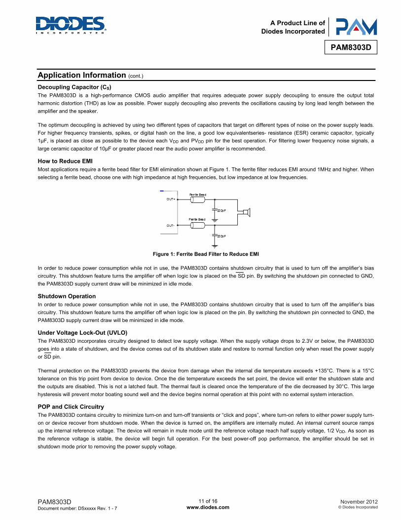
Decoupling Capacitor (CS) The PAM8303D is a high-performance CMOS audio amplifier that requires adequate power supply decoupling to ensure the output total harmonic distortion (THD) as low as possible. Power supply decoupling also prevents the oscillations causing by long lead length between the amplifier and the speaker. The optimum decoupling is achieved by using two different types of capacitors that target on different types of noise on the power supply leads. For higher frequency transients, spikes, or digital hash on the line, a good low equivalentseries- resistance (ESR) ceramic capacitor, typically 1µF, is placed as close as possible to the device each VDD and PVDD pin for the best operation. For filtering lower frequency noise signals, a large ceramic capacitor of 10µF or greater placed near the audio power amplifier is recommended. How to Reduce EMI Most applications require a ferrite bead filter for EMI elimination shown at Figure 1. The ferrite filter reduces EMI around 1MHz and higher. When selecting a ferrite bead, choose one with high impedance at high frequencies, but low impedance at low frequencies.
Figure 1: Ferrite Bead Filter to Reduce EMI
In order to reduce power consumption while not in use, the PAM8303D contains shutdown circuitry that is used to turn off the amplifier’s bias circuitry. This shutdown feature turns the amplifier off when logic low is placed on the SD pin. By switching the shutdown pin connected to GND, the PAM8303D supply current draw will be minimized in idle mode. Shutdown Operation In order to reduce power consumption while not in use, the PAM8303D contains shutdown circuitry that is used to turn off the amplifier’s bias circuitry. This shutdown feature turns the amplifier off when logic low is placed on the pin. By switching the shutdown pin connected to GND, the PAM8303D supply current draw will be minimized in idle mode. Under Voltage Lock-Out (UVLO) The PAM8303D incorporates circuitry designed to detect low supply voltage. When the supply voltage drops to 2.3V or below, the PAM8303D goes into a state of shutdown, and the device comes out of its shutdown state and restore to normal function only when reset the power supply or SD pin. Thermal protection on the PAM8303D prevents the device from damage when the internal die temperature exceeds +135°C. There is a 15°C tolerance on this trip point from device to device. Once the die temperature exceeds the set point, the device will enter the shutdown state and the outputs are disabled. This is not a latched fault. The thermal fault is cleared once the temperature of the die decreased by 30°C. This large hysteresis will prevent motor boating sound well and the device begins normal operation at this point with no external system interaction. POP and Click Circuitry The PAM8303D contains circuitry to minimize turn-on and turn-off transients or “click and pops”, where turn-on refers to either power supply turn-on or device recover from shutdown mode. When the device is turned on, the amplifiers are internally muted. An internal current source ramps up the internal reference voltage. The device will remain in mute mode until the reference voltage reach half supply voltage, 1/2 VDD. As soon as the reference voltage is stable, the device will begin full operation. For the best power-off pop performance, the amplifier should be set in shutdown mode prior to removing the power supply voltage.
PAM8303D Document number: DSxxxxx Rev. 1 - 7
12 of 16 www.diodes.com
November 2012© Diodes Incorporated
PAM8303D
A Product Line ofDiodes Incorporated
Application Information (cont.)
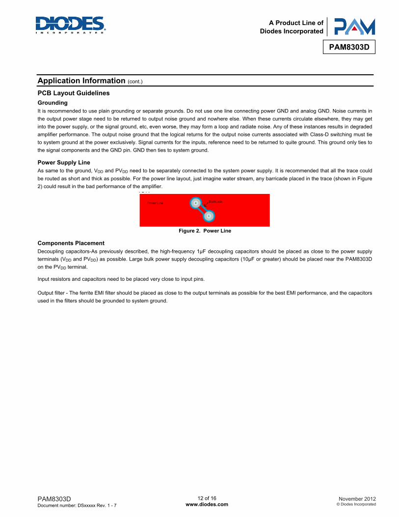
PCB Layout Guidelines Grounding It is recommended to use plain grounding or separate grounds. Do not use one line connecting power GND and analog GND. Noise currents in the output power stage need to be returned to output noise ground and nowhere else. When these currents circulate elsewhere, they may get into the power supply, or the signal ground, etc, even worse, they may form a loop and radiate noise. Any of these instances results in degraded amplifier performance. The output noise ground that the logical returns for the output noise currents associated with Class-D switching must tie to system ground at the power exclusively. Signal currents for the inputs, reference need to be returned to quite ground. This ground only ties to the signal components and the GND pin. GND then ties to system ground. Power Supply Line As same to the ground, VDD and PVDD need to be separately connected to the system power supply. It is recommended that all the trace could be routed as short and thick as possible. For the power line layout, just imagine water stream, any barricade placed in the trace (shown in Figure 2) could result in the bad performance of the amplifier.
Figure 2. Power Line
Components Placement Decoupling capacitors-As previously described, the high-frequency 1µF decoupling capacitors should be placed as close to the power supply terminals (VDD and PVDD) as possible. Large bulk power supply decoupling capacitors (10µF or greater) should be placed near the PAM8303D on the PVDD terminal. Input resistors and capacitors need to be placed very close to input pins. Output filter - The ferrite EMI filter should be placed as close to the output terminals as possible for the best EMI performance, and the capacitors used in the filters should be grounded to system ground.

PAM8303D Document number: DSxxxxx Rev. 1 - 7
13 of 16 www.diodes.com
November 2012© Diodes Incorporated
PAM8303D
A Product Line ofDiodes Incorporated
Ordering Information
Part Number Part Marking Package Type Standard Package
PAM8303DBYC P8303D XXXYW DFN3x3-8 3000 Units/Tape&Reel
PAM8303DBSC P8303D XXXYW MSOP-8 2500 Units/Tape&Reel
Marking Information
PAM8303D Document number: DSxxxxx Rev. 1 - 7
14 of 16 www.diodes.com
November 2012© Diodes Incorporated
PAM8303D
A Product Line ofDiodes Incorporated
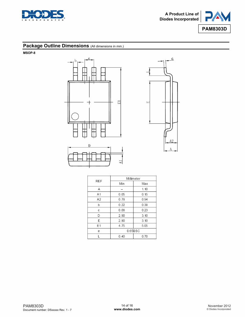
Package Outline Dimensions (All dimensions in mm.) MSOP-8

PAM8303D Document number: DSxxxxx Rev. 1 - 7
15 of 16 www.diodes.com
November 2012© Diodes Incorporated
PAM8303D
A Product Line ofDiodes Incorporated
Package Outline Dimensions (cont.) (All dimensions in mm.) DFN3x3-8
PAM8303D Document number: DSxxxxx Rev. 1 - 7
16 of 16 www.diodes.com
November 2012© Diodes Incorporated
PAM8303D
A Product Line ofDiodes Incorporated
IMPORTANT NOTICE DIODES INCORPORATED MAKES NO WARRANTY OF ANY KIND, EXPRESS OR IMPLIED, WITH REGARDS TO THIS DOCUMENT, INCLUDING, BUT NOT LIMITED TO, THE IMPLIED WARRANTIES OF MERCHANTABILITY AND FITNESS FOR A PARTICULAR PURPOSE (AND THEIR EQUIVALENTS UNDER THE LAWS OF ANY JURISDICTION). Diodes Incorporated and its subsidiaries reserve the right to make modifications, enhancements, improvements, corrections or other changes without further notice to this document and any product described herein. Diodes Incorporated does not assume any liability arising out of the application or use of this document or any product described herein; neither does Diodes Incorporated convey any license under its patent or trademark rights, nor the rights of others. Any Customer or user of this document or products described herein in such applications shall assume all risks of such use and will agree to hold Diodes Incorporated and all the companies whose products are represented on Diodes Incorporated website, harmless against all damages. Diodes Incorporated does not warrant or accept any liability whatsoever in respect of any products purchased through unauthorized sales channel. Should Customers purchase or use Diodes Incorporated products for any unintended or unauthorized application, Customers shall indemnify and hold Diodes Incorporated and its representatives harmless against all claims, damages, expenses, and attorney fees arising out of, directly or indirectly, any claim of personal injury or death associated with such unintended or unauthorized application. Products described herein may be covered by one or more United States, international or foreign patents pending. Product names and markings noted herein may also be covered by one or more United States, international or foreign trademarks. This document is written in English but may be translated into multiple languages for reference. Only the English version of this document is the final and determinative format released by Diodes Incorporated.
LIFE SUPPORT Diodes Incorporated products are specifically not authorized for use as critical components in life support devices or systems without the express written approval of the Chief Executive Officer of Diodes Incorporated. As used herein: A. Life support devices or systems are devices or systems which: 1. are intended to implant into the body, or
2. support or sustain life and whose failure to perform when properly used in accordance with instructions for use provided in the labeling can be reasonably expected to result in significant injury to the user.
B. A critical component is any component in a life support device or system whose failure to perform can be reasonably expected to cause the failure of the life support device or to affect its safety or effectiveness. Customers represent that they have all necessary expertise in the safety and regulatory ramifications of their life support devices or systems, and acknowledge and agree that they are solely responsible for all legal, regulatory and safety-related requirements concerning their products and any use of Diodes Incorporated products in such safety-critical, life support devices or systems, notwithstanding any devices- or systems-related information or support that may be provided by Diodes Incorporated. Further, Customers must fully indemnify Diodes Incorporated and its representatives against any damages arising out of the use of Diodes Incorporated products in such safety-critical, life support devices or systems. Copyright © 2012, Diodes Incorporated www.diodes.com