Embed Size (px)
Citation preview

DESIGN AND AUTOMATION OF VOLTAGE-SCALED CLOCK NETWORKS
A Thesis
Submitted to the Faculty
of
Drexel University
by
Ahmet Can Sitik
in partial fulfillment of the
requirements for the degree
of
Doctor of Philosophy
December 2015

c© Copyright 2015Ahmet Can Sitik. All Rights Reserved.

ii
Acknowledgments
This PhD study has been with its ups and downs, and I would like to take this opportunity thank individ-
uals who have helped me during my PhD journey. Without the support, guidance, and friendship of these
individuals, this study would not be possible.
I would like to first thank my advisor, Prof. Baris Taskin, for giving me this opportunity. He has trusted
in my abilities and let me choose my own research direction. This trust has helped me grow as a researcher
and an engineer. I appreciate his time for long discussions, and his initiatives in industry to help grow my
research through collaborations and internships.
I wish to thank my committee members Prof. Nagarajan Kandasamy, Prof. Caglan Kumbur, Prof. Prawat
Nagvajara and Prof. Ioannis Savidis for their encouragement, feedback and direction. All the current and
former members of the Drexel VLSI Lab have provided productive collaborations, advice and kept a positive
working environment. They include Leo Filippini, Swetha George, Dr. Vinayak Honkote, Scott Lerner, Dr.
Jianchao Lu, Michael Lui, Dr. Ankit More, Vasil Pano, Karthik “Paco” Sangaiah, Sharat Shekar, and Dr.
Ying Teng. I would like to specifically thank Ankit for being a friend and a mentor in my first years of PhD
journey, and mentoring me through my Intel journey in my final year. I would also like to acknowledge my
collaborators at Stony Brook University NanoCAS Lab, Weicheng Liu, and Prof. Emre Salman, for their
cooperation, discussion and feedback.
I would like to thank my collaborators in industry for their cooperation, guidance and feedback. They
include Benjamin Huang, Dr. Savithri Sundareswaran and Anis Jarrar from Freescale Semiconductor, Noor
Elahi from Texas Instruments, and Ravinder Rachala from AMD. Their feedback helped me improve my
research ideas and gave me a chance to tackle real world problems of the microelectronics industry.
I would like to thank my supervisors and mentors at my two internship experiences. I would like to thank
Dr. Kayhan Kucukcakar for giving me the opportunity to intern at PrimeTime, and his continued guidance
and discussion to broaden my perspective in physical design research. I would also like to thank my mentors
Dr. Li Ding and Dr. Ruijing Shen for their guidance, and patience with me. I would like to thank Dr. Dinesh

iii
Somasekhar, my supervisor at Intel, for the opportunity, and his guidance throughout my journey to prepare
me for my future career at Intel. I would like to thank my mentors Dr. Ankit More, Emily J. Shriver, and Dr.
Ahmed Abousamra for the weekly discussions, and helping me solidify my ideas throughout the project.
All my friends in Philadelphia who were with me through the ups and downs of my PhD journey. I would
like to extend special thanks to Prof. Ertan Agar, Basak Doyran, Cem Guvener, Prof. Utku Kursat Ercan,
Emre Olceroglu, and Dr. Reyhan Taspinar for being great friends.
I would like to thank my parents, Mehmet and Zeynep Sitik, to whom this thesis is also dedicated, for
their love and support.

iv
Table of Contents
LIST OF TABLES . . . . . . . . . . . . . . . . . . . . . . . . . . . . . . . . . . . . . . . . . . . . . ix
LIST OF FIGURES . . . . . . . . . . . . . . . . . . . . . . . . . . . . . . . . . . . . . . . . . . . . . xiii
ABSTRACT . . . . . . . . . . . . . . . . . . . . . . . . . . . . . . . . . . . . . . . . . . . . . . . . xv
1. INTRODUCTION . . . . . . . . . . . . . . . . . . . . . . . . . . . . . . . . . . . . . . . . . . 1
1.1 Problem Statement . . . . . . . . . . . . . . . . . . . . . . . . . . . . . . . . . . . . . . . . 2
1.2 Contributions of the Dissertation . . . . . . . . . . . . . . . . . . . . . . . . . . . . . . . . . 3
1.2.1 Contributions on Low Swing Clocking . . . . . . . . . . . . . . . . . . . . . . . . . . . . 3
1.2.2 Contributions on Multi-Voltage Single-Clock Domain Clock Mesh Design . . . . . . . . . 4
1.3 Organization of the Dissertation . . . . . . . . . . . . . . . . . . . . . . . . . . . . . . . . . 5
2. VOLTAGE-SCALED CLOCK DISTRIBUTION NETWORKS . . . . . . . . . . . . . . . . 6
2.1 Low Swing Clock Trees . . . . . . . . . . . . . . . . . . . . . . . . . . . . . . . . . . . . . . 8
2.1.1 Single-Vdd vs. Dual-Vdd Low Swing Clocking . . . . . . . . . . . . . . . . . . . . . . . . 8
2.1.2 Low Swing Clocking with Conventional Flip-Flops . . . . . . . . . . . . . . . . . . . . . 8
2.1.3 Low Swing Clocking with Low Swing-Aware Flip-Flops . . . . . . . . . . . . . . . . . . 12
2.1.4 Low Swing Clocking in FinFET Technology . . . . . . . . . . . . . . . . . . . . . . . . . 18
2.1.5 Low Swing Clocking in Gated Clock Trees . . . . . . . . . . . . . . . . . . . . . . . . . 21
2.2 Multi-Voltage Single-Clock Domain Clock Distribution Networks . . . . . . . . . . . . . . . 23
2.2.1 Multi-Voltage Clocking with Clock Tree Topology . . . . . . . . . . . . . . . . . . . . . 24
2.2.2 Multi-Voltage Clocking with Clock Mesh Topology . . . . . . . . . . . . . . . . . . . . . 25
2.2.3 Effect of PVT Variations in Multi-Voltage Clocking . . . . . . . . . . . . . . . . . . . . . 25
3. FEASIBILITY STUDY OF LOW SWING CLOCKING . . . . . . . . . . . . . . . . . . . . 28
3.1 Introduction . . . . . . . . . . . . . . . . . . . . . . . . . . . . . . . . . . . . . . . . . . . . 28
3.2 Observations on Local Timing . . . . . . . . . . . . . . . . . . . . . . . . . . . . . . . . . . 30
3.3 Methodology . . . . . . . . . . . . . . . . . . . . . . . . . . . . . . . . . . . . . . . . . . . 33
v
3.3.1 Buffer Characterization . . . . . . . . . . . . . . . . . . . . . . . . . . . . . . . . . . . . 34
3.3.2 Iterative Skew Minimization . . . . . . . . . . . . . . . . . . . . . . . . . . . . . . . . . 35
3.4 Experimental Analysis . . . . . . . . . . . . . . . . . . . . . . . . . . . . . . . . . . . . . . 39
3.4.1 Simulation Setup . . . . . . . . . . . . . . . . . . . . . . . . . . . . . . . . . . . . . . . 39
3.4.2 Results . . . . . . . . . . . . . . . . . . . . . . . . . . . . . . . . . . . . . . . . . . . . . 40
3.5 Conclusion . . . . . . . . . . . . . . . . . . . . . . . . . . . . . . . . . . . . . . . . . . . . 42
4. DESIGN AUTOMATION FOR LOW SWING CLOCKING . . . . . . . . . . . . . . . . . . 44
4.1 Introduction . . . . . . . . . . . . . . . . . . . . . . . . . . . . . . . . . . . . . . . . . . . . 44
4.2 Methodology . . . . . . . . . . . . . . . . . . . . . . . . . . . . . . . . . . . . . . . . . . . 46
4.2.1 Low Swing DFF Design . . . . . . . . . . . . . . . . . . . . . . . . . . . . . . . . . . . 46
4.2.2 Clock Timing Modeling . . . . . . . . . . . . . . . . . . . . . . . . . . . . . . . . . . . . 50
4.2.3 Slew-Aware Low Swing CTS . . . . . . . . . . . . . . . . . . . . . . . . . . . . . . . . . 51
4.3 Experimental Analysis . . . . . . . . . . . . . . . . . . . . . . . . . . . . . . . . . . . . . . 53
4.3.1 Simulation Setup . . . . . . . . . . . . . . . . . . . . . . . . . . . . . . . . . . . . . . . 53
4.3.2 Results at 45nm Technology . . . . . . . . . . . . . . . . . . . . . . . . . . . . . . . . . 54
4.3.3 Results at 32nm Technology . . . . . . . . . . . . . . . . . . . . . . . . . . . . . . . . . 55
4.3.4 Discussion on the Effect of Interconnect Resistance . . . . . . . . . . . . . . . . . . . . . 56
4.4 Conclusion . . . . . . . . . . . . . . . . . . . . . . . . . . . . . . . . . . . . . . . . . . . . 56
5. FINFET-BASED LOW SWING CLOCKING . . . . . . . . . . . . . . . . . . . . . . . . . . 65
5.1 Introduction . . . . . . . . . . . . . . . . . . . . . . . . . . . . . . . . . . . . . . . . . . . . 65
5.2 Methodology . . . . . . . . . . . . . . . . . . . . . . . . . . . . . . . . . . . . . . . . . . . 67
5.2.1 FinFET-Based Clock Buffer Design . . . . . . . . . . . . . . . . . . . . . . . . . . . . . 68
5.2.2 Timing Characterization of the FinFET-Based Clock Buffer Design . . . . . . . . . . . . . 69
5.2.3 Low Swing DFF Design . . . . . . . . . . . . . . . . . . . . . . . . . . . . . . . . . . . 69
5.2.4 Low Swing Clock Tree Design . . . . . . . . . . . . . . . . . . . . . . . . . . . . . . . . 71
5.3 Experimental Analysis . . . . . . . . . . . . . . . . . . . . . . . . . . . . . . . . . . . . . . 73
5.3.1 Simulation Setup . . . . . . . . . . . . . . . . . . . . . . . . . . . . . . . . . . . . . . . 73

vi
5.3.2 Low Swing vs. Full Swing Clocking in FinFET Technology . . . . . . . . . . . . . . . . . 75
5.3.3 FinFET-based Low Swing Clocking for High Performance . . . . . . . . . . . . . . . . . 77
5.3.4 FinFET-based Low Swing Clocking for Ultra Low Power . . . . . . . . . . . . . . . . . . 78
5.3.5 Leakage Power Comparison . . . . . . . . . . . . . . . . . . . . . . . . . . . . . . . . . 79
5.4 Conclusion . . . . . . . . . . . . . . . . . . . . . . . . . . . . . . . . . . . . . . . . . . . . 80
6. AN IMPROVED ALGORITHM FORSLEW-DRIVEN CLOCK TREE SYNTHESIS . . . . . . . . . . . . . . . . . . . . . . . . . . 81
6.1 Introduction . . . . . . . . . . . . . . . . . . . . . . . . . . . . . . . . . . . . . . . . . . . . 81
6.2 Deferred Merge Embedding (DME) . . . . . . . . . . . . . . . . . . . . . . . . . . . . . . . 84
6.2.1 Step 1: Merging Pair Selection . . . . . . . . . . . . . . . . . . . . . . . . . . . . . . . . 84
6.2.2 Step 2: Merging Point Computation . . . . . . . . . . . . . . . . . . . . . . . . . . . . . 85
6.2.3 Step 3: Net Splitting . . . . . . . . . . . . . . . . . . . . . . . . . . . . . . . . . . . . . 86
6.3 Proposed Improvements over DME . . . . . . . . . . . . . . . . . . . . . . . . . . . . . . . . 86
6.3.1 Step 1: Improvements in Merging Pair Selection . . . . . . . . . . . . . . . . . . . . . . . 86
6.3.2 Step 2: Improvements in Merging Point Computation . . . . . . . . . . . . . . . . . . . . 87
6.3.3 Step 3: Improvements in Net Splitting . . . . . . . . . . . . . . . . . . . . . . . . . . . . 90
6.4 Experimental Analysis . . . . . . . . . . . . . . . . . . . . . . . . . . . . . . . . . . . . . . 92
6.4.1 Simulation Setup . . . . . . . . . . . . . . . . . . . . . . . . . . . . . . . . . . . . . . . 92
6.4.2 Results at 45nm Planar CMOS Technology . . . . . . . . . . . . . . . . . . . . . . . . . 93
6.4.3 Results at 20nm FinFET Technology . . . . . . . . . . . . . . . . . . . . . . . . . . . . . 95
6.4.4 Run Time Analysis . . . . . . . . . . . . . . . . . . . . . . . . . . . . . . . . . . . . . . 97
6.5 Conclusion . . . . . . . . . . . . . . . . . . . . . . . . . . . . . . . . . . . . . . . . . . . . 98
7. AN IMPROVED ALGORITHM FORLOW SWING GATED CLOCK TREE SYNTHESIS . . . . . . . . . . . . . . . . . . . . . . 99
7.1 Introduction . . . . . . . . . . . . . . . . . . . . . . . . . . . . . . . . . . . . . . . . . . . . 99
7.2 Background . . . . . . . . . . . . . . . . . . . . . . . . . . . . . . . . . . . . . . . . . . . . 100
7.3 Methodology . . . . . . . . . . . . . . . . . . . . . . . . . . . . . . . . . . . . . . . . . . . 102
7.3.1 DME Method with Proposed Improvements . . . . . . . . . . . . . . . . . . . . . . . . . 102

vii
7.3.2 Local Clock Tree Synthesis . . . . . . . . . . . . . . . . . . . . . . . . . . . . . . . . . . 104
7.3.3 Top-Level Clock Tree Synthesis . . . . . . . . . . . . . . . . . . . . . . . . . . . . . . . 105
7.3.4 Complexity Analysis . . . . . . . . . . . . . . . . . . . . . . . . . . . . . . . . . . . . . 107
7.4 Experimental Analysis . . . . . . . . . . . . . . . . . . . . . . . . . . . . . . . . . . . . . . 108
7.4.1 Simulation Setup . . . . . . . . . . . . . . . . . . . . . . . . . . . . . . . . . . . . . . . 108
7.4.2 Experimental Results . . . . . . . . . . . . . . . . . . . . . . . . . . . . . . . . . . . . . 109
7.4.3 Run Time Analysis . . . . . . . . . . . . . . . . . . . . . . . . . . . . . . . . . . . . . . 111
7.5 Conclusion . . . . . . . . . . . . . . . . . . . . . . . . . . . . . . . . . . . . . . . . . . . . 111
8. MULTI-VOLTAGE SINGLE-CLOCK DOMAINCLOCK MESH DESIGN . . . . . . . . . . . . . . . . . . . . . . . . . . . . . . . . . . . . . . 113
8.1 Introduction . . . . . . . . . . . . . . . . . . . . . . . . . . . . . . . . . . . . . . . . . . . . 113
8.2 Methodology . . . . . . . . . . . . . . . . . . . . . . . . . . . . . . . . . . . . . . . . . . . 114
8.2.1 Mesh Size Selection . . . . . . . . . . . . . . . . . . . . . . . . . . . . . . . . . . . . . . 115
8.2.2 Pre-mesh Driver Selection . . . . . . . . . . . . . . . . . . . . . . . . . . . . . . . . . . 116
8.2.3 Pre-mesh Tree Synthesis . . . . . . . . . . . . . . . . . . . . . . . . . . . . . . . . . . . 117
8.3 An Improved Methodology for Variation-Awareness . . . . . . . . . . . . . . . . . . . . . . . 118
8.3.1 Pre-mesh Driver Selection . . . . . . . . . . . . . . . . . . . . . . . . . . . . . . . . . . 119
8.3.2 Multi-Corner-Aware Pre-mesh Tree Synthesis . . . . . . . . . . . . . . . . . . . . . . . . 120
8.4 Experimental Analysis . . . . . . . . . . . . . . . . . . . . . . . . . . . . . . . . . . . . . . 122
8.4.1 Simulation Setup . . . . . . . . . . . . . . . . . . . . . . . . . . . . . . . . . . . . . . . 122
8.4.2 Results for Single-Corner Analysis . . . . . . . . . . . . . . . . . . . . . . . . . . . . . . 123
8.4.3 Results for Multi-Corner Analysis . . . . . . . . . . . . . . . . . . . . . . . . . . . . . . 126
8.5 Conclusion . . . . . . . . . . . . . . . . . . . . . . . . . . . . . . . . . . . . . . . . . . . . 128
9. CONCLUSIONS AND FUTURE DIRECTIVES . . . . . . . . . . . . . . . . . . . . . . . . 130
9.1 Conclusions . . . . . . . . . . . . . . . . . . . . . . . . . . . . . . . . . . . . . . . . . . . . 130
9.1.1 Conclusions on Low Swing Clock Trees . . . . . . . . . . . . . . . . . . . . . . . . . . . 130
9.1.2 Conclusions on Multi-Voltage Single-Clock Domain Mesh . . . . . . . . . . . . . . . . . 131
9.2 Future Directives . . . . . . . . . . . . . . . . . . . . . . . . . . . . . . . . . . . . . . . . . 131

viii
9.2.1 Future Directives on Low Swing Clock Trees . . . . . . . . . . . . . . . . . . . . . . . . 132
9.2.2 Future Directives on Multi-Voltage Single-Clock Domain Clock Mesh . . . . . . . . . . . 132
BIBLIOGRAPHY . . . . . . . . . . . . . . . . . . . . . . . . . . . . . . . . . . . . . . . . . . . . . . 133
VITA . . . . . . . . . . . . . . . . . . . . . . . . . . . . . . . . . . . . . . . . . . . . . . . . . . . . 138
ix
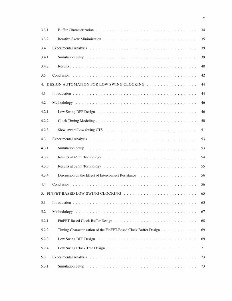
List of Tables
2.1 The comparison of full swing and low swing insertion delay characteristics at 20nm FinFET and32nm planar CMOS technologies for s38584. . . . . . . . . . . . . . . . . . . . . . . . . . . . 20
2.2 The leakage power consumption comparison of low swing and full swing implementations ofclock trees built on s38584, in 20nm FinFET and 32nm planar CMOS technologies. . . . . . . . 22
2.3 Insertion delay profile of the motivational clock tree example at two voltage domains shown inFigure 2.15. The maximum and the minimum insertion delays that define the global skew aremarked with bold. . . . . . . . . . . . . . . . . . . . . . . . . . . . . . . . . . . . . . . . . . . 26
2.4 Improved skew values with a delay insertion to the 1.2V Domain. . . . . . . . . . . . . . . . . 27
3.1 Measured TTS values, and the effect of a low swing clock supply on the local timing (average andmaximum slack decrease) under the same clock slew. The decreased slack, induced by increasedclock-to-q delay, is traded off for the power savings of low swing clocks. . . . . . . . . . . . . . 32
3.2 A typical lookup table for NBUFFX8 of Synopsys SAED Library at 80% of Vdd . The typicalcapacitance is found to be 45fF at a 100ps slew constraint, using the OPTIMIZE function ofHSPICE. The parent buffer (Level-1) is fixed at NBUFFX8, and the child buffer (Level-2) isvaried to observe the effect of sizing on delay. . . . . . . . . . . . . . . . . . . . . . . . . . . . 36
3.3 Normalized power and skew comparison against a full swing (FS) clock tree (CT), and an un-optimized low swing (LS) clock tree (CT) synthesized by IC Compiler, at 0.90×Vdd . Time-to-switch (TTS) constraint is at 88.5ps for this case and is satisfied at all benchmarks. . . . . . . . 41
3.4 Normalized power and skew comparison against a full swing (FS) clock tree (CT), and an un-optimized low swing (LS) clock tree (CT) synthesized by IC Compiler, at 0.85×Vdd . Time-to-switch (TTS) constraint is at 93.7ps for this case and is satisfied at all benchmarks. . . . . . . . 41
3.5 Normalized power and skew comparison against a full swing (FS) clock tree (CT), and an un-optimized low swing (LS) clock tree (CT) synthesized by IC Compiler, at 0.80×Vdd . Time-to-switch (TTS) constraint is at 99.5ps for this case and is satisfied at all benchmarks. . . . . . . . 42
3.6 Number of iterations and number of buffers modified for each benchmark circuit at fractions ofVdd levels. . . . . . . . . . . . . . . . . . . . . . . . . . . . . . . . . . . . . . . . . . . . . . . 42
4.1 Power-delay product comparison of the proposed LSDFF and conventional FSDFF as a functionof clock swing. . . . . . . . . . . . . . . . . . . . . . . . . . . . . . . . . . . . . . . . . . . . 49
4.2 Floorplan area, number of DFFs, and number of gates information of the benchmark circuits. . . 53
4.3 The comparison of clock tree power (CP in mW), DFF power (DFFP in mW), clock skew (Sk. inps), clock slew (Sl. in ps) and the clock-to-q delay (C2Q in ps) for the baseline full swing (FS),the low swing (LS) implementation with the methodology introduced in Chapter 3, and proposedlow swing (LS) methodology for 45nm technology along with wire 1 running at 1 GHz and worstcase corner. Low swing clock voltage is at 0.65×Vdd . . . . . . . . . . . . . . . . . . . . . . . . 58

x
4.4 The comparison of clock tree power (CP in mW), DFF power (DFFP in mW), clock skew (Sk. inps), clock slew (Sl. in ps) and the clock-to-q delay (C2Q in ps) for the baseline full swing (FS),the low swing (LS) implementation with the methodology introduced in Chapter 3, and proposedlow swing (LS) methodology for 45nm technology with wire 2 running at 1 GHz and worst casecorner. Low swing clock voltage is at 0.75×Vdd . . . . . . . . . . . . . . . . . . . . . . . . . . . 59
4.5 The comparison of clock tree power (CP in mW), DFF power (DFFP in mW), clock skew (Sk. inps), clock slew (Sl. in ps) and the clock-to-q delay (C2Q in ps) for the baseline full swing (FS),the low swing (LS) implementation with the methodology introduced in Chapter 3, and proposedlow swing (LS) methodology for 45nm technology with wire 1 running at 1.5 GHz and worstcase corner. Low swing clock voltage is at 0.75×Vdd . . . . . . . . . . . . . . . . . . . . . . . . 60
4.6 The comparison of clock tree power (CP in mW), DFF power (DFFP in mW), clock skew (Sk. inps), clock slew (Sl. in ps) and the clock-to-q delay (C2Q in ps) for the baseline full swing (FS),the low swing (LS) implementation with the methodology introduced in Chapter 3, and proposedlow swing (LS) methodology for 32nm technology with wire 1 running at 1 GHz and worst casecorner. Low swing clock voltage is at 0.75×Vdd . . . . . . . . . . . . . . . . . . . . . . . . . . . 61
4.7 The comparison of clock tree power (CP in mW), DFF power (DFFP in mW), clock skew (Sk. inps), clock slew (Sl. in ps) and the clock-to-q delay (C2Q in ps) for the baseline full swing (FS),the low swing (LS) implementation with the methodology introduced in Chapter 3, and proposedlow swing (LS) methodology for 32nm technology with wire 2 running at 1 GHz and worst casecorner. Low swing clock voltage is at 0.80×Vdd . . . . . . . . . . . . . . . . . . . . . . . . . . . 62
4.8 The comparison of clock tree power (CP in mW), DFF power (DFFP in mW), clock skew (Sk. inps), clock slew (Sl. in ps) and the clock-to-q delay (C2Q in ps) for the baseline full swing (FS),the low swing (LS) implementation with the methodology introduced in Chapter 3, and proposedlow swing (LS) methodology for 32nm technology with wire 1 running at 1.5 GHz and worstcase corner. Low swing clock voltage is at 0.90×Vdd . . . . . . . . . . . . . . . . . . . . . . . . 63
4.9 The comparison of clock tree power (CP in mW), DFF power (DFFP in mW), clock skew (Sk. inps), clock slew (Sl. in ps) and the clock-to-q delay (C2Q in ps) for the baseline full swing (FS),the low swing (LS) implementation with the methodology introduced in Chapter 3, and proposedlow swing (LS) methodology for 32nm technology with wire 2 running at 1.5 GHz and worstcase corner. Low swing clock voltage is at 0.95×Vdd . . . . . . . . . . . . . . . . . . . . . . . . 64
5.1 The comparison of the custom-designed FinFET-based buffer and the planar CMOS-based NBUFFX32of SAED 32nm library. . . . . . . . . . . . . . . . . . . . . . . . . . . . . . . . . . . . . . . . 69
5.2 The clock-to-q delay (C2Q) and the power consumption comparison of the conventional DFFtopology and the proposed low swing DFF topology in 20nm FinFET technology. . . . . . . . . 71
5.3 The comparison of clock buffer metrics (number of clock buffers/total buffer capacitance) andthe clock interconnect metrics (total interconnect length/total interconnect capacitance) betweenthe FinFET-based low swing (LS) and FinFET-based full swing (FS) clock trees, reported withthe information on benchmark circuits. . . . . . . . . . . . . . . . . . . . . . . . . . . . . . . . 75
5.4 The performance and power comparison of FinFET-based low swing (LS) and FinFET-based fullswing (FS) clock trees at 3 GHz, reported separately for the clock network and the DFF cells. . . 76
5.5 The performance and power comparison of planar CMOS-based low swing and planar CMOS-based full swing clock trees at 1.5 GHz, reported separately for the clock network and the DFFcells. . . . . . . . . . . . . . . . . . . . . . . . . . . . . . . . . . . . . . . . . . . . . . . . . . 77

xi
5.6 The clock tree power (excluding DFF) comparison of the proposed FinFET-based low swing (LS)clocking against the FinFET-based full swing (FS) clocking (both at 3 GHz), and planar CMOS-based low swing (LS) and full swing (FS) clocking (both at 1.5 GHz), normalized to FinFET-based low swing. . . . . . . . . . . . . . . . . . . . . . . . . . . . . . . . . . . . . . . . . . . 78
5.7 The total (clock network+DFF) power comparison of the proposed FinFET-based low swing (LS)clocking against the FinFET-based full swing (FS) clocking (both at 3 GHz), and planar CMOS-based low swing (LS) and full swing (FS) clocking (both at 1.5 GHz), normalized to FinFET-based low swing. . . . . . . . . . . . . . . . . . . . . . . . . . . . . . . . . . . . . . . . . . . 78
5.8 The clock tree power (excluding DFF) comparison of the proposed FinFET-based low swing (LS)clocking against the FinFET-based full swing (FS) clocking (both at 1.5 GHz), and planar CMOS-based low swing (LS) and full swing (FS) clocking (both at 1.5 GHz), normalized to FinFET-based low swing. . . . . . . . . . . . . . . . . . . . . . . . . . . . . . . . . . . . . . . . . . . 79
5.9 The total (clock network+DFF) power comparison of the proposed FinFET-based low swing (LS)clocking against the FinFET-based full swing (FS) clocking (both at 1.5 GHz), and planar CMOS-based low swing (LS) and full swing (FS) clocking (both at 1.5 GHz), normalized to FinFET-based low swing. . . . . . . . . . . . . . . . . . . . . . . . . . . . . . . . . . . . . . . . . . . 79
5.10 The leakage power comparison at low swing (LS) and full swing (FS) of both 20nm FinFET and32nm planar CMOS technologies in µW. . . . . . . . . . . . . . . . . . . . . . . . . . . . . . . 80
6.1 Experimental setup for each step: Pair Selection (Step 1 in Figure 6.1), Merging Point Computa-tion (Step 2 in Figure 6.1) and Net Splitting (Step 3 in Figure 6.1). . . . . . . . . . . . . . . . . 93
6.2 Experiments 1 and 2 to demonstrate the impact of the proposed pair selection and merging pointcomputation schemes with reported clock slew (Sl.), clock skew (Sk.), and clock power (CP) atthe worst PVT corner of 1 GHz and 0.90×Vdd in 45nm planar CMOS technology. . . . . . . . 94
6.3 Experiments 1 and 2 to demonstrate the impact of the proposed pair selection and merging pointcomputation schemes with reported clock slew (Sl.), clock skew (Sk.), and clock power (CP) atthe worst PVT corner of 1 GHz and 0.63×Vdd in 45nm planar CMOS technology. . . . . . . . 94
6.4 Experiments 1 and 2 to demonstrate the impact of the proposed pair selection and merging pointcomputation schemes with reported clock slew (Sl.), clock skew (Sk.), and clock power (CP) atthe worst PVT corner of 2 GHz and 0.90×Vdd in 20nm FinFET technology. . . . . . . . . . . . 95
6.5 Experiments 1 and 2 to demonstrate the impact of the proposed pair selection and merging pointcomputation schemes with reported clock slew (Sl.), clock skew (Sk.), and clock power (CP) atthe worst PVT corner of 2 GHz and 0.63×Vdd in 20nm FinFET technology. . . . . . . . . . . . 95
6.6 Experiments 1 and 2 to demonstrate the impact of the proposed pair selection and merging pointcomputation schemes with reported clock slew (Sl.), clock skew (Sk.), and clock power (CP) atthe worst PVT corner of 3 GHz and 0.90×Vdd in 20nm FinFET technology. . . . . . . . . . . . 96
6.7 Experiments 1 and 2 to demonstrate the impact of the proposed pair selection and merging pointcomputation schemes with reported clock slew (Sl.), clock skew (Sk.), and clock power (CP) atthe worst PVT corner of 3 GHz and 0.72×Vdd in 20nm FinFET technology. . . . . . . . . . . . 96
6.8 Run time comparison of all cases in 45nm planar CMOS technology at 1 GHz and 0.63×Vdd , inseconds. . . . . . . . . . . . . . . . . . . . . . . . . . . . . . . . . . . . . . . . . . . . . . . . 98
7.1 The floorplan size and the total number of clock sinks of benchmark circuits. . . . . . . . . . . 108
xii
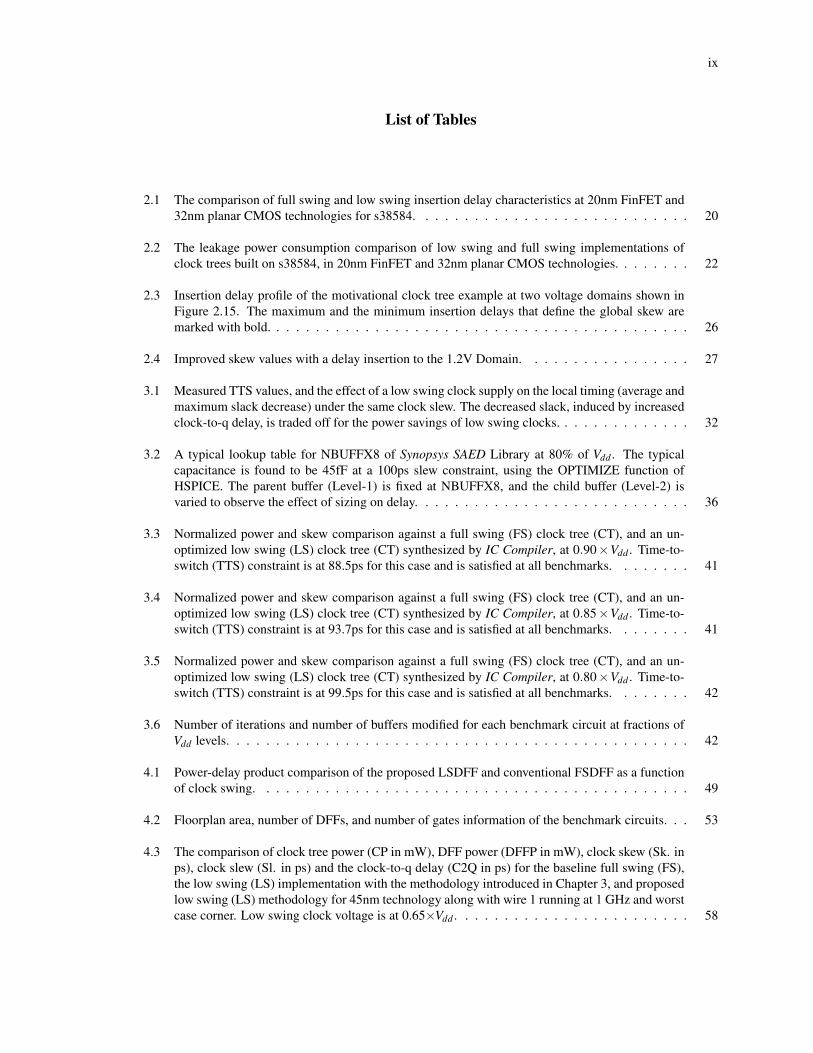
7.2 The number of clock sinks at each clock gate cluster and the percentage of gated clock sinksusing the configuration shown in Figure 7.5. . . . . . . . . . . . . . . . . . . . . . . . . . . . . 110
7.3 The comparison of clock tree power (CP), clock skew (Sk.) and clock slew (Sl.) of gated clocktree synthesis methodology in [45], the combination of the gated clock tree methodology in [45]and the prescribed skew methodology in [8], and the proposed gated clock tree synthesis method-ology, operating at 0.675V and 1.5 GHz in 45nm technology. . . . . . . . . . . . . . . . . . . . 110
7.4 Run time comparison of three methodologies in seconds. . . . . . . . . . . . . . . . . . . . . . 111
8.1 The power and the skew trade-off of the proposed methodology against clock networks synthe-sized by IC Compiler (ICC). . . . . . . . . . . . . . . . . . . . . . . . . . . . . . . . . . . . . 125
8.2 Created benchmark circuits. . . . . . . . . . . . . . . . . . . . . . . . . . . . . . . . . . . . . 126
8.3 Power comparison of improved multi-corner-aware multi-voltage clock mesh methodology (IM-CAMV Mesh) over single-voltage domain mesh (SV Mesh) synthesized by IC Compiler (ICC)and single-corner-aware multi-voltage clock mesh methodology (SCAMV Mesh) at best cor-ner (BC), nominal corner (NC), and worst corner (WC) in mW. . . . . . . . . . . . . . . . . . . 127
8.4 Skew comparison of improved multi-corner-aware multi-voltage clock mesh methodology (IM-CAMV Mesh) over single-voltage domain mesh (SV Mesh) synthesized by IC Compiler (ICC)and single-corner-aware multi-voltage clock mesh methodology (SCA Mesh) at best corner (BC),nominal corner (NC), and worst corner (WC) in ps, overall skew is bold. . . . . . . . . . . . . . 128
xiii
List of Figures
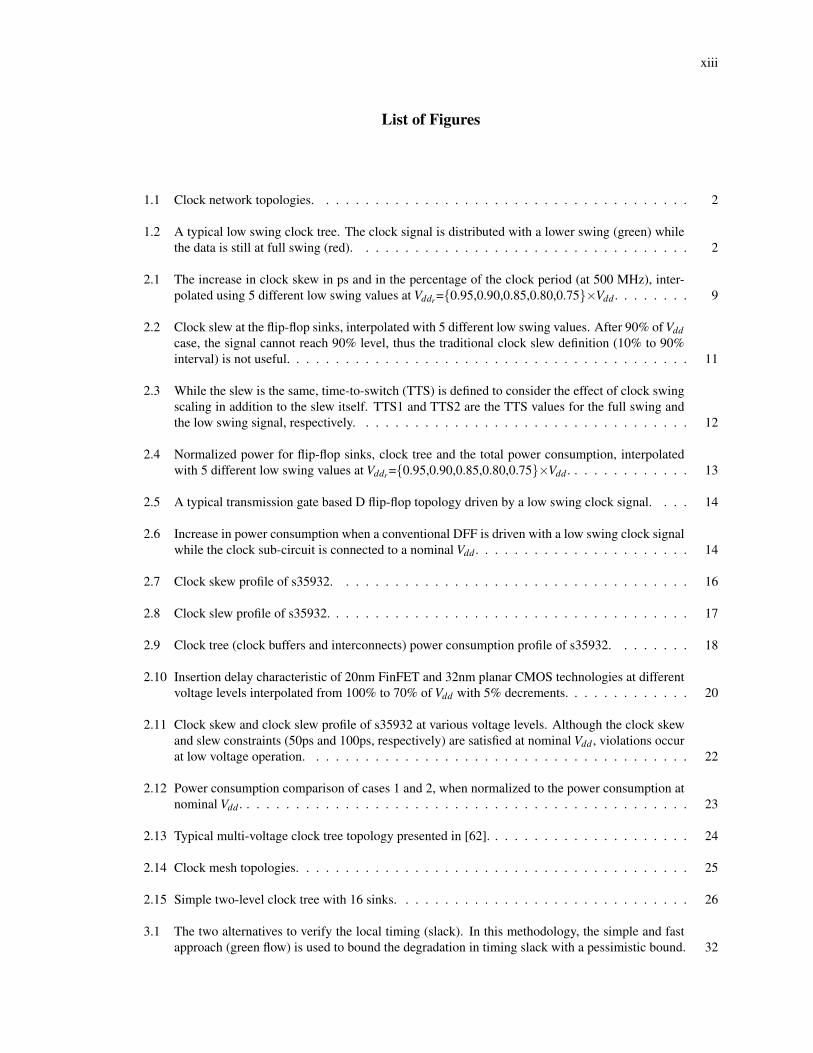
1.1 Clock network topologies. . . . . . . . . . . . . . . . . . . . . . . . . . . . . . . . . . . . . . 2
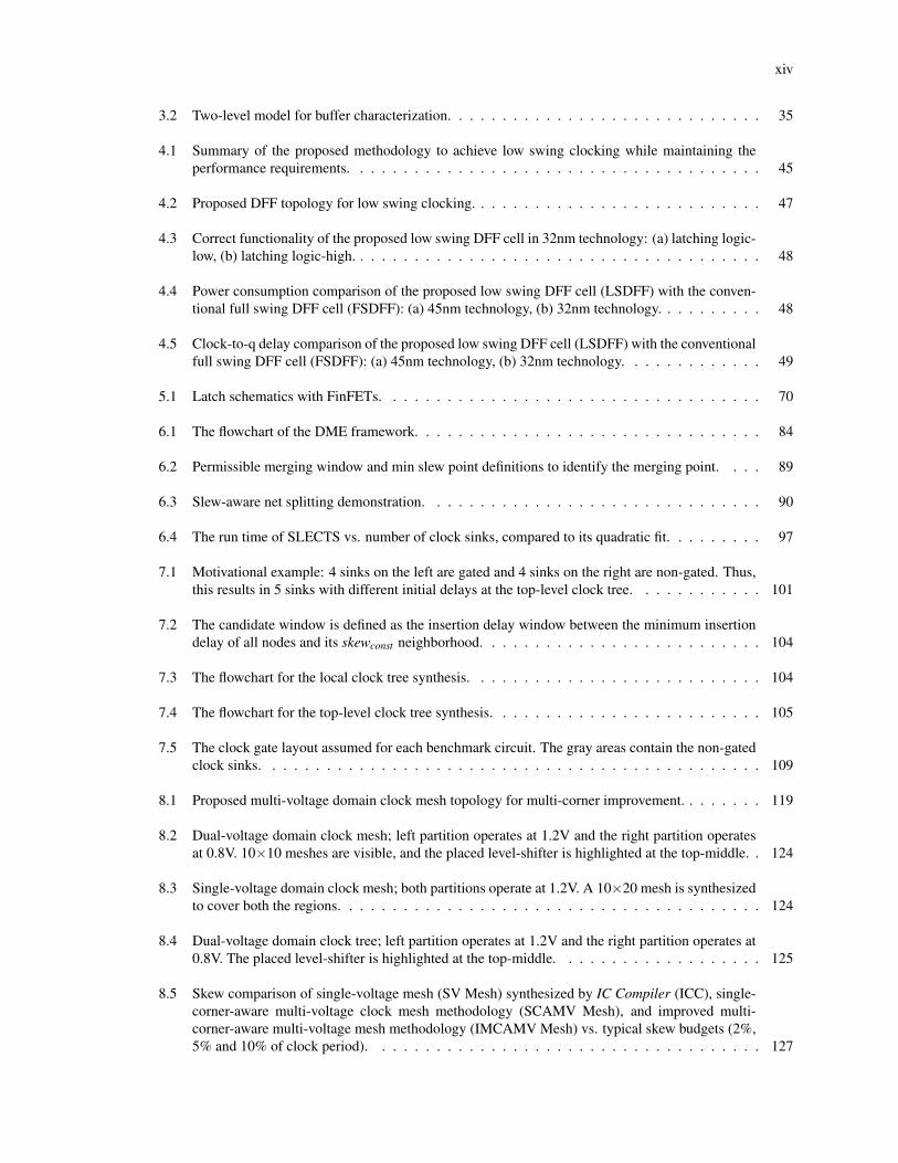
1.2 A typical low swing clock tree. The clock signal is distributed with a lower swing (green) whilethe data is still at full swing (red). . . . . . . . . . . . . . . . . . . . . . . . . . . . . . . . . . 2
2.1 The increase in clock skew in ps and in the percentage of the clock period (at 500 MHz), inter-polated using 5 different low swing values at Vddr =0.95,0.90,0.85,0.80,0.75×Vdd . . . . . . . . 9
2.2 Clock slew at the flip-flop sinks, interpolated with 5 different low swing values. After 90% of Vddcase, the signal cannot reach 90% level, thus the traditional clock slew definition (10% to 90%interval) is not useful. . . . . . . . . . . . . . . . . . . . . . . . . . . . . . . . . . . . . . . . . 11
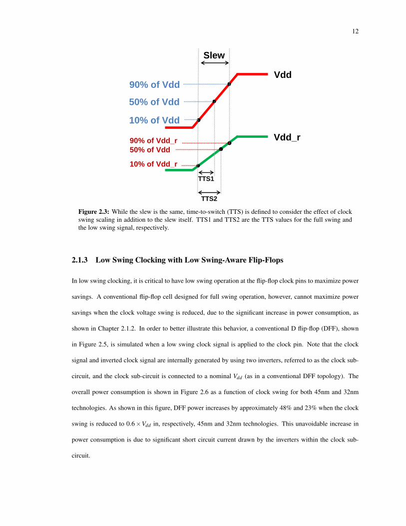
2.3 While the slew is the same, time-to-switch (TTS) is defined to consider the effect of clock swingscaling in addition to the slew itself. TTS1 and TTS2 are the TTS values for the full swing andthe low swing signal, respectively. . . . . . . . . . . . . . . . . . . . . . . . . . . . . . . . . . 12
2.4 Normalized power for flip-flop sinks, clock tree and the total power consumption, interpolatedwith 5 different low swing values at Vddr =0.95,0.90,0.85,0.80,0.75×Vdd . . . . . . . . . . . . . 13
2.5 A typical transmission gate based D flip-flop topology driven by a low swing clock signal. . . . 14
2.6 Increase in power consumption when a conventional DFF is driven with a low swing clock signalwhile the clock sub-circuit is connected to a nominal Vdd . . . . . . . . . . . . . . . . . . . . . . 14
2.7 Clock skew profile of s35932. . . . . . . . . . . . . . . . . . . . . . . . . . . . . . . . . . . . 16
2.8 Clock slew profile of s35932. . . . . . . . . . . . . . . . . . . . . . . . . . . . . . . . . . . . . 17
2.9 Clock tree (clock buffers and interconnects) power consumption profile of s35932. . . . . . . . 18
2.10 Insertion delay characteristic of 20nm FinFET and 32nm planar CMOS technologies at differentvoltage levels interpolated from 100% to 70% of Vdd with 5% decrements. . . . . . . . . . . . . 20
2.11 Clock skew and clock slew profile of s35932 at various voltage levels. Although the clock skewand slew constraints (50ps and 100ps, respectively) are satisfied at nominal Vdd , violations occurat low voltage operation. . . . . . . . . . . . . . . . . . . . . . . . . . . . . . . . . . . . . . . 22
2.12 Power consumption comparison of cases 1 and 2, when normalized to the power consumption atnominal Vdd . . . . . . . . . . . . . . . . . . . . . . . . . . . . . . . . . . . . . . . . . . . . . . 23
2.13 Typical multi-voltage clock tree topology presented in [62]. . . . . . . . . . . . . . . . . . . . . 24
2.14 Clock mesh topologies. . . . . . . . . . . . . . . . . . . . . . . . . . . . . . . . . . . . . . . . 25
2.15 Simple two-level clock tree with 16 sinks. . . . . . . . . . . . . . . . . . . . . . . . . . . . . . 26
3.1 The two alternatives to verify the local timing (slack). In this methodology, the simple and fastapproach (green flow) is used to bound the degradation in timing slack with a pessimistic bound. 32
xiv
3.2 Two-level model for buffer characterization. . . . . . . . . . . . . . . . . . . . . . . . . . . . . 35
4.1 Summary of the proposed methodology to achieve low swing clocking while maintaining theperformance requirements. . . . . . . . . . . . . . . . . . . . . . . . . . . . . . . . . . . . . . 45
4.2 Proposed DFF topology for low swing clocking. . . . . . . . . . . . . . . . . . . . . . . . . . . 47
4.3 Correct functionality of the proposed low swing DFF cell in 32nm technology: (a) latching logic-low, (b) latching logic-high. . . . . . . . . . . . . . . . . . . . . . . . . . . . . . . . . . . . . . 48
4.4 Power consumption comparison of the proposed low swing DFF cell (LSDFF) with the conven-tional full swing DFF cell (FSDFF): (a) 45nm technology, (b) 32nm technology. . . . . . . . . . 48
4.5 Clock-to-q delay comparison of the proposed low swing DFF cell (LSDFF) with the conventionalfull swing DFF cell (FSDFF): (a) 45nm technology, (b) 32nm technology. . . . . . . . . . . . . 49
5.1 Latch schematics with FinFETs. . . . . . . . . . . . . . . . . . . . . . . . . . . . . . . . . . . 70
6.1 The flowchart of the DME framework. . . . . . . . . . . . . . . . . . . . . . . . . . . . . . . . 84
6.2 Permissible merging window and min slew point definitions to identify the merging point. . . . 89
6.3 Slew-aware net splitting demonstration. . . . . . . . . . . . . . . . . . . . . . . . . . . . . . . 90
6.4 The run time of SLECTS vs. number of clock sinks, compared to its quadratic fit. . . . . . . . . 97
7.1 Motivational example: 4 sinks on the left are gated and 4 sinks on the right are non-gated. Thus,this results in 5 sinks with different initial delays at the top-level clock tree. . . . . . . . . . . . 101
7.2 The candidate window is defined as the insertion delay window between the minimum insertiondelay of all nodes and its skewconst neighborhood. . . . . . . . . . . . . . . . . . . . . . . . . . 104
7.3 The flowchart for the local clock tree synthesis. . . . . . . . . . . . . . . . . . . . . . . . . . . 104
7.4 The flowchart for the top-level clock tree synthesis. . . . . . . . . . . . . . . . . . . . . . . . . 105
7.5 The clock gate layout assumed for each benchmark circuit. The gray areas contain the non-gatedclock sinks. . . . . . . . . . . . . . . . . . . . . . . . . . . . . . . . . . . . . . . . . . . . . . 109
8.1 Proposed multi-voltage domain clock mesh topology for multi-corner improvement. . . . . . . . 119
8.2 Dual-voltage domain clock mesh; left partition operates at 1.2V and the right partition operatesat 0.8V. 10×10 meshes are visible, and the placed level-shifter is highlighted at the top-middle. . 124
8.3 Single-voltage domain clock mesh; both partitions operate at 1.2V. A 10×20 mesh is synthesizedto cover both the regions. . . . . . . . . . . . . . . . . . . . . . . . . . . . . . . . . . . . . . . 124
8.4 Dual-voltage domain clock tree; left partition operates at 1.2V and the right partition operates at0.8V. The placed level-shifter is highlighted at the top-middle. . . . . . . . . . . . . . . . . . . 125
8.5 Skew comparison of single-voltage mesh (SV Mesh) synthesized by IC Compiler (ICC), single-corner-aware multi-voltage clock mesh methodology (SCAMV Mesh), and improved multi-corner-aware multi-voltage mesh methodology (IMCAMV Mesh) vs. typical skew budgets (2%,5% and 10% of clock period). . . . . . . . . . . . . . . . . . . . . . . . . . . . . . . . . . . . 127
xv
AbstractDESIGN AND AUTOMATION OF VOLTAGE-SCALED CLOCK NETWORKS
Ahmet Can SitikAdvisor: Baris Taskin, Ph.D.
In this dissertation, a vital step of VLSI physical design flow, synthesis of clock distribution networks, is
investigated. Clock network synthesis (CNS) involves large and complex optimization problems to achieve
high performance and low power demands of current integrated circuits (ICs). Ineffectiveness of existing
methodologies to provide high performance at lower voltage nodes is the main driver for this dissertation
research. A design and automation flow for voltage-scaled clock networks is proposed to satisfy tight timing
constraints at high frequency (for high performance) and low voltage (for low power) operation.
One implementation of voltage-scaled clock networks is low (voltage) swing clocking, which is a known
technique, yet its applicability remains limited to designs with low performance demands. In this dissertation,
novel methodologies are introduced to i) apply low swing clocking to legacy designs as a power saving
methodology, ii) develop a complete CNS flow for low swing clocking of high performance ICs. These
methodologies include slew-driven approaches that are better suited to future transistor and interconnect
technologies. Second implementation of voltage-scaled clock networks is multi-voltage clocking, which is
another known technique, yet its applicability remains limited to clock tree topology. In this dissertation,
multi-voltage clocking with a clock mesh topology is investigated in order to address a missing aspect in the
current IC design flows.
Practical considerations of the current IC design flows are also investigated in this dissertation to expand
the applicability of the proposed CNS flow. A novel methodology is introduced to facilitate clock gating
within low swing clocking. The applicability of low swing clocking to FinFET technology, which is currently
the industry norm, is shown to be effective.


1
Chapter 1: INTRODUCTION
Clock distribution networks synchronize all sequential elements in an integrated circuit (IC), therefore, they
are vital for timing closure to ensure correct functionality of the IC. Comprising generous resources to deliver
this timing closure, power consumption of the clock network is 30% of the total IC power dissipation [44]. To
this end, design methodologies for CNS are well-studied in the literature and industrial applications to address
the trade-off between timing performance and power consumption [43, 22, 41, 14, 1, 32, 23, 8, 46, 33]. There
are two topologies that have been used for clock distribution networks: 1) Clock tree topology, shown in
Figure 1.1(a), is preferred in low power ICs due to its lower power consumption [23, 8, 46, 33], and 2) clock
mesh topology, shown in Figure 1.1(b), is preferred in high end microprocessor design due to its high timing
performance, despite higher power consumption [43, 22, 41, 14, 1, 32].
One of the well-known techniques to reduce power consumption is to scale down supply voltage swing.
To this end, voltage-scaled clock distribution networks are promising candidates for low power ICs, consid-
ering the significance of clock power consumption. In this dissertation, two aspects of voltage-scaled clock
networks is studied: Low swing clocking and multi-voltage clocking. Low swing clocking is one of the
considered techniques for low power design [39, 2, 64, 36] where the voltage swing of the clock distribu-
tion network is scaled down, while the voltage swing of the rest of the IC (sequential and combinational
logic) is kept at the higher swing in order not to degrade timing in local paths, as shown in Figure 1.2. In
low swing clocking, the power savings on the clock buffers and interconnects obtained through the voltage
scaling trades off clock timing performance, due to higher delay and slower switching (slew) at the clock
sinks (i.e. clock pins of sequential cells). Another technique is to consider multi-voltage designs where the
IC is split into different voltage domains with different performance targets and power budgets. In the par-
ticular case of multi-voltage single-clock domain ICs, synchronization of the clock sinks in the low voltage
domain to the ones in high voltage domain presents a challenge. Although clock tree topology is investigated
for multi-voltage single-clock domain ICs [62, 63], clock mesh topology, which is known to have high tim-
ing performance and immunity to process-voltage-temperature (PVT) variations, is not previously studied.
2
(a) Typical clock tree topology. (b) Typical clock mesh topology.
Figure 1.1: Clock network topologies.
Figure 1.2: A typical low swing clock tree. The clock signal is distributed with a lower swing while thedata is still at full swing.
In this dissertation, the challenges of low swing clocking are addressed, and the use of clock meshes for
multi-voltage single-clock domain ICs is investigated methodically.
1.1 Problem Statement
Voltage-scaled clock networks at reduced voltage swings achieve significant power savings while trading
off timing performance, thereby limiting the applicability of voltage-scaled clock networks to ICs with low
performance demands. To this end, achieving higher timing performance while preserving power savings
of voltage-scaled clock networks is the main problem investigated in this dissertation, in order to extend the
applicability of voltage-scaled clock networks. In particular, two themes of voltage-scaled clock networks

3
are studied in this dissertation. In the first theme, low swing clocking is studied to address the challenges that
degrades the timing performance (clock skew and slew) while preserving the power savings through voltage
scaling. In the second theme, multi-voltage single-clock domain clock meshes are introduced to minimize
power consumption through voltage scaling while preserving the high timing performance of clock mesh
topology.
1.2 Contributions of the Dissertation
The major contribution of this dissertation is to enable high timing performance while achieving significant
power savings through voltage scaling. In Chapter 1.2.1, proposed methodologies that address the challenges
of low swing clocking in high performance ICs are introduced. In Chapter 1.2.2, proposed methodologies
that address the challenges of implementing clock mesh topology in multi-voltage ICs are introduced.
1.2.1 Contributions on Low Swing Clocking
The current art of low swing clocking is effective for low power applications that do not demand high perfor-
mance [39, 2, 64, 36]. The applicability of low swing clocking remains limited for high performance designs
due to the following issues: i) Larger number of buffers and greater interconnect delay increase the insertion
delay on the clock path, leading to excessive clock skew, ii) increased switching time at the clock buffer out-
put (clock slew), leading to excessive buffering to satisfy timing constraints, iii) the effect of the low swing
clock on the local timing and flip-flop power consumption when synchronizing flip-flop cells running at full
data swing, iv) the decrease in the expected power savings of the low swing clocking operation, induced by
the efforts to minimize performance degradation, and v) the lack of practical considerations that current CNS
tools have, such as clock-gating, limiting the applicability of low swing clocking.
In this dissertation, the following novel methodologies are introduced in order to:
1. perform a feasibility study of low swing clocking by optimizing legacy full swing clock trees, address-
ing challenges (i) and (iv) [55, 56],
2. develop a novel slew-aware low swing clock tree and flip-flop design flow in order not to degrade clock
slew and local timing, addressing challenges (i), (ii), (iii), and (iv) [48, 49, 50],

4
3. extend the applicability of low swing clocking flow to FinFET technology [51],
4. develop a novel slew-driven clock tree synthesis flow in order to better address the timing challenges
of low swing clocking for the current and future interconnect technologies, and further improve power
savings [29],
5. facilitate clock gating in low swing clocking flow, addressing challenge (v).
1.2.2 Contributions on Multi-Voltage Single-Clock Domain Clock Mesh Design
Multi-voltage single-clock domain clock distribution networks with a tree topology is a popular technique
used for low-power design methodology with sophisticated automation techniques existent in industrial tool
flows. Multi-voltage single-clock domain clock trees are designed to deliver clock signal with local trees
in each voltage domain and these trees are connected at the upper level through level shifters [62]. What
is missing in the literature and in automation flows is the combination of the clock mesh topology and the
multi-voltage clocking techniques. To this end, the contribution in this dissertation is presented exclusively
targeting clock mesh topology. Multi-voltage single-clock domain clock mesh design is not a straight-forward
process, due to following challenges: i) a single clock mesh is not feasible as its electrically-shorted mesh
wires cannot drive the voltage sinks operating at different voltage levels, therefore, separate meshes are
needed for each domain, ii) the skew among these domains must be balanced, which is a challenge that
arises due to the isolation among the domains, iii) the skew introduced by the variation must be analyzed
and bounded considering multiple PVT corners, as isolated pre-mesh trees in different voltage domains have
different characteristics under PVT variations.
In this dissertation, a multi-voltage single-clock domain clock mesh design is introduced for the first time,
while addressing the listed challenges methodically. In particular, the following methodologies are proposed
in order to:
1. perform a feasibility study of multi-voltage domain clock mesh design, addressing challenges (i) and
(ii) [52],
2. develop an improved algorithm to consider PVT variations in multi-voltage clock mesh synthesis,
addressing challenges (i), (ii), and (iii) [53, 54].

5
1.3 Organization of the Dissertation
The dissertation is organized as follows. In Chapter 2, the preliminaries and the background information
of low swing clocking and multi-voltage domain clock distribution networks are presented. In Chapter 3,
the feasibility of low swing clocking is shown with a novel low swing clock tree optimization methodology
applied to legacy clock trees. In Chapter 4, the novel slew-aware low swing clock tree and flip-flop design
methodology is proposed. In Chapter 5, the applicability of low swing clocking is extended to FinFET
technology with a novel methodology that addresses unique challenges in FinFET technology. In Chapter 6,
a novel slew-driven clock tree synthesis methodology is proposed to address the timing challenges of the
current and future interconnect technologies more efficiently, and further improve power savings of low
swing clocking. In Chapter 7, a novel methodology is introduced in order to facilitate clock gating in low
swing clocking flow. In Chapter 8, the multi-voltage single-clock domain clock mesh design methodology is
proposed. In Chapter 9, the dissertation is finalized with concluding remarks and discussion of future work.

6
Chapter 2: VOLTAGE-SCALED CLOCK DISTRIBUTION NETWORKS
With increasing complexity in digital IC design along with rapid increase in the clock frequency and reducing
feature size, timing closure and power consumption have become major concerns in the VLSI industry [26].
The clock distribution network is vital for the synchronism of sequential cells, and it consumes 30% of total
on-chip power [44].
The synchronism of clock distribution network is defined by clock skew, which is the time difference
between the maximum and the minimum arrival times (t i) of all clock sinks (S):
skew = max∀i ∈ S
t i− min∀i ∈ S
t i. (2.1)
Furthermore, PVT variations affect the clock arrival time, contributing to clock skew. The common approach
in CNS is to define a skew budget, which can be zero, resulting in zero-skew clock networks, or a non-zero
bound that is a percentage of the clock period, resulting in bounded-skew clock networks. Clock tree topology
can be designed for zero, or bounded skew, yet it is susceptible to PVT variations. On the other hand, clock
mesh topology has low clock skew and tolerant to PVT variations, thanks to the short circuit connection of
clock mesh balancing out all arrival times. The integrity of the clock signal is another important metric to
guarantee that the clock signal reaches to all clock sinks. The integrity of the clock signal is defined by the
clock slew, which is the rise (fall) time of the clock signal at a sink i, measured from 10% (90%) to 90% (10%)
of its voltage swing:
slewi = t iV @90%− t i
V @10%. (2.2)
The common approach in CNS is to define a slew budget that is a percentage of the clock period to bound
clock slew of all sinks. Clock buffer insertion is performed to decrease clock slew within a bound, which
requires less clock buffers in clock tree topology due to less interconnect capacitance, whereas it requires
significantly more clock buffers in clock mesh topology due to the high interconnect capacitance of clock
mesh wiring. Clock skew and clock slew define the timing performance of clock distribution networks.

7
Power consumption is another concern for clock distribution networks. Due to the large capacitance of
clock buffers and interconnects switching at every cycle, dynamic power consumption of clock networks are
significantly high. Dynamic power consumption is given by the equation:
Pdyn = αCtotal fV 2dd (2.3)
where α is the activity factor, Ctotal is total capacitance, f is operation frequency and Vdd is the supply
voltage swing. Based on Eq. (2.3), the power minimization can be performed through clock activity or total
capacitance minimization, or lowering frequency or clock voltage swing. As lowering clock voltage swing
has the most significant effect (quadratic vs. linear), voltage-scaled clock distribution networks are promising
candidates for low power ICs.
A direct solution to minimize the overall on-chip power dissipation is to reduce the supply voltage. But
this reduction in supply voltage is at the cost of degradation in the performance of the design [13]. Another
solution is low swing clocking where voltage swing of the clock network is reduced while preserving the
voltage swing at the local paths in order not to degrade local timing performance. With the clock distribu-
tion network and flip-flops being the major contributors to the overall on-chip power dissipation, low swing
clocking is one of the highly considered techniques for low power design [39, 2, 64, 36]. In low swing clock
trees, presented in Chapter 2.1, the power savings on the clock buffers and interconnects obtained through
the voltage scaling trades off timing performance (clock skew and slew).
Another solution to reduce IC power consumption is to consider multi-voltage designs where the IC is
split into different voltage domains with different performance targets and power budgets. Thus, the overall IC
performance is not degraded by keeping the high performance demand blocks in the higher voltage domains,
and significant power savings are achieved in the lower voltage domains. However, in the particular case of
multi-voltage single-clock domain ICs, presented in Chapter 2.2, synchronization of clock sinks in different
voltage domain presents a unique challenge [62, 63], thereby degrading clock skew.

8
2.1 Low Swing Clock Trees
The comparison between single- and dual-Vdd low swing clocking implementations is discussed in Chap-
ter 2.1.1. The implications of low swing clocking on timing performance and power consumption with and
without low swing-aware flip-flop designs are analyzed in Chapter 2.1.2 and Chapter 2.1.3, respectively. In
order to study the implications of technology scaling on low swing clocking, timing and power consumption
trends are analyzed at 20nm FinFET technology in Chapter 2.1.4. The implications on timing performance
and power consumption in low swing gated clock trees are discussed in Chapter 2.1.5.
2.1.1 Single-Vdd vs. Dual-Vdd Low Swing Clocking
The implementation of low swing clocking can be realized in two ways depending on the number of unique
voltage sources on the chip: Single- or dual-Vdd configurations. In the single-Vdd implementation, it is
assumed that the only power grid available in the design is the full swing Vdd . Thus, the implementation of
low swing clocking includes level converting and low swing buffers in order to create and manipulate the low
swing voltage level [2]. This implementation is the only option when another power grid is not pre-planned,
because the overhead of creating another power grid can be cost prohibitive. It is observed that the single-Vdd
design implementation is not the ideal case for low swing clocking as the low swing voltage level obtained
with this implementation may not be robust, and this implementation consumes greater leakage power [2].
Alternatively, in most contemporary designs, especially for the low power implementations, additional
power grids are already pre-planned (and placed before the clock tree synthesis step). Thus, it is compliant
with common practice to assume the presence of a low swing power grid. This is the preferred implementation
method in this dissertation, in order to fully benefit from low swing clocking. Assuming the presence of a low
swing power grid (or multiple grids) floorplanned to be used for low power applications of the logic circuit,
the clock tree also benefits from a low swing grid in order to further decrease the power consumption, making
this approach a perfect candidate for low power applications.
2.1.2 Low Swing Clocking with Conventional Flip-Flops
A practical approach of low swing clocking is to convert a full swing clock tree built by an high quality CNS
tool to a low swing clock tree, in order for short-term applicability and integration with the existing industrial

9
0.750.80.850.90.9510
10
20
30
x Vdd
Incr
. in
Clo
ck S
kew
(ps
)
0.750.80.850.90.9510
0.5
1
1.5
Incr
. in
Clo
ck S
kew
(%
of T
)
Figure 2.1: The increase in clock skew in ps and in the percentage of the clock period (at 500 MHz),interpolated using 5 different low swing values at Vddr =0.95,0.90,0.85,0.80,0.75×Vdd .
flows. The disadvantage of this practical approach is the potential degradation in clock skew and clock slew,
and the negative effects of a low swing clock on the full (data) swing flip-flop sinks, which has a direct effect
on local timing (slack), and power consumption of flip-flop cells. To this end, observations on clock skew,
clock slew and power consumption are presented in this subsection.
Timing performance (clock skew and slew) and power consumption of a clock tree highly depend on
the supply voltage of its clock buffers and load capacitance that consists of the buffer, sink and interconnect
capacitances. There are known simple first order or more complex higher order models that can estimate
timing and power consumption of clock buffers using capacitance information for a known fixed supply
voltage Vdd [25, 40, 57]. However, a dedicated model is needed for this low swing implementation: A low
swing clock tree driving register sinks operating with full swing data input/output but with low swing clock
input. For this purpose, accurate SPICE simulations are performed for analysis. The changes in timing and
power consumption of the largest circuit of ISCAS’89 benchmarks, s35932, are monitored in 90nm planar
CMOS technology at 500 MHz.
Decrease in clock voltage increases clock buffer delay, increasing insertion delay of a clock tree. The
increase in insertion delay potentially increases clock skew in low swing operation. To this end, the change

10
in clock skew with respect to the change in the supply voltage of the clock buffers (i.e. low swing voltage
Vddr ) from 100% to 75% of the Vdd with 5% decrements is observed, and presented in Figure 2.1. It is shown
that the skew increases with decreasing low swing voltage level.
It is well-known that clock slew directly impacts timing slack on local data paths [60]. In the standard
VLSI design flow, clock slew is constrained to a practical maximum limit, helping define local timing (slack)
budgets. However, the traditional slew definition, i.e. the transition time between 10% and 90% of Vdd , is
meaningless for low swing clocks as the signal cannot reach 90% level when the low swing voltage is smaller
than 90% of the full swing, shown in Figure 2.2. Furthermore, when a low swing clock signal drives full
swing flip-flops, the impact on timing slack is more than the value of clock slew alone. This is because clock
voltage swing directly impacts the clock-to-q delay of flip-flop cells, thereby impacting timing slack in the
timing budget. Even if clock slew is kept the same as the clock slew constraint at full swing, a low swing
clock signal may cause a negative effect on the local timing (slack). In order to account for this effect, a new
term called time-to-switch (TTS) is defined as the time elapsed from 10% of the low swing clock to 50% of
the original full swing. TTS is a measure to reflect the time elapsed before the clock pin of a flip-flop cell
switches its state, as the flip-flop, unlike clock buffers, still runs at full swing. With this new definition, the
effect of the low swing clock is more accurately included into the timing constraint. In effect, TTS enables
the reflection of the timing properties of a low swing clock signal with the exact same slew as the original
full swing clock, which is very important for this implementation of low swing clocking.
For a full swing signal, TTS is expected to be approximately half of its slew value (TTS1 in Figure 2.3),
whereas a larger value is expected for a lower swing signal (TTS2 in Figure 2.3), as it takes longer to switch
with the low swing clock signal. The TTS definition considers the effect of low swing clock on the local tim-
ing, and this negative effect can be bounded by introducing a TTS constraint, along with the slew constraint.
It is argued at this point that if the negative impacts of the low swing clock are analyzed and measured with
this TTS definition, then the negative impacts on the timing slack of the actual circuit are bounded with these
measured values, when the TTS constraint is satisfied.
As for the power consumption, the reduction of the supply voltage of the clock buffers for low swing
operation is expected to decrease the power consumption of the clock tree. However, applying a low swing

11
0.750.80.850.90.9510
100
200
300
400
x Vdd
Clo
ck S
lew
(ps
)
0.750.80.850.90.9510
5
10
15
20
Clo
ck S
lew
(%
of T
)
Figure 2.2: Clock slew at the flip-flop sinks, interpolated with 5 different low swing values. After 90%of Vdd case, the signal cannot reach 90% level, thus the traditional clock slew definition (10% to 90%interval) is not useful.
clock signal to the flip-flops operating at the full swing data may increase the power consumption of flip-flop
cells due to the increase in short circuit power. In order to analyze these phenomena, the power dissipation of
individual parts of a low swing clock network is profiled while decreasing low swing voltage level on the clock
buffers. In Figure 2.4, power consumption of the clock tree (excluding flip-flop cells), power consumption
of the flip-flop cells (excluding clock tree), and the total power consumption (clock tree+flip-flop cells) are
shown individually. As expected, the power consumption of the clock tree decreases (almost) quadratically
with linearly decreasing low swing voltage level. On the other hand, the power consumption of the flip-flop
cells are observed to increase significantly. Due to this contrast, the total power consumption needs to be
analyzed carefully to understand the overall effect of a low swing clock driving full swing flip-flops. It is
shown in Figure 2.4 that the total power consumption decreases until 80% of Vdd , and starts increasing with
further decreased clock voltage swing. This “soft spot” occurs when the increase in the power consumption
of the flip-flop cells starts outweighing the power savings in the clock tree at lower swing levels. This
observation demonstrates that scaling the clock tree voltage level indefinitely, e.g. beyond less than 80% of
the nominal Vdd , is not advantageous for this sample experimental setup.
12
Vdd
Vdd_r
50% of Vdd
Slew
TTS1
50% of Vdd
10% of Vdd
90% of Vdd
TTS2
10% of Vdd_r
90% of Vdd_r
Figure 2.3: While the slew is the same, time-to-switch (TTS) is defined to consider the effect of clockswing scaling in addition to the slew itself. TTS1 and TTS2 are the TTS values for the full swing andthe low swing signal, respectively.
2.1.3 Low Swing Clocking with Low Swing-Aware Flip-Flops
In low swing clocking, it is critical to have low swing operation at the flip-flop clock pins to maximize power
savings. A conventional flip-flop cell designed for full swing operation, however, cannot maximize power
savings when the clock voltage swing is reduced, due to the significant increase in power consumption, as
shown in Chapter 2.1.2. In order to better illustrate this behavior, a conventional D flip-flop (DFF), shown
in Figure 2.5, is simulated when a low swing clock signal is applied to the clock pin. Note that the clock
signal and inverted clock signal are internally generated by using two inverters, referred to as the clock sub-
circuit, and the clock sub-circuit is connected to a nominal Vdd (as in a conventional DFF topology). The
overall power consumption is shown in Figure 2.6 as a function of clock swing for both 45nm and 32nm
technologies. As shown in this figure, DFF power increases by approximately 48% and 23% when the clock
swing is reduced to 0.6×Vdd in, respectively, 45nm and 32nm technologies. This unavoidable increase in
power consumption is due to significant short circuit current drawn by the inverters within the clock sub-
circuit.

13
0.750.80.850.90.9510.4
0.5
0.6
0.7
0.8
0.9
1
1.1
1.2
1.3
Nor
mal
ized
Pow
er
% of Vdd
DFF SinksClock NetworkTotal
Figure 2.4: Normalized power for flip-flop sinks, clock tree and the total power consumption, interpo-lated with 5 different low swing values at Vddr =0.95,0.90,0.85,0.80,0.75×Vdd .
In the typical DFF cell shown in Figure 2.5, clock signals drive both NMOS and PMOS transistors. If
the same DFF topology is used with a low swing clock signal by supplying a low Vdd to the clock sub-
circuit (whereas the data signal is still at full swing to maintain performance), the PMOS transistors driven
by the clock signal fail to completely turn off when the clock signal is high. For example, consider a 45nm
technology with a nominal Vdd of 1V. If the clock swing is reduced to 0.7V, the gate-to-source voltage of
the PMOS transistors becomes -0.3V since the data signal is at full swing and the inverters within the flip-
flop are connected to nominal (full swing) Vdd (unlike the inverters in the clock sub-circuit). Since -0.3V is
sufficiently close to the threshold voltage of PMOS transistors in this technology, this behavior significantly
affects the operation reliability of a traditional DFF cell driven by a low swing clock signal. As an example,
consider a rising-edge triggered master-slave flip-flop. When the clock signal is high, the master latch should
be turned off. However, due to low swing clock signal, the transmission gate (or tri-state inverter) within the
master latch cannot completely turn off. If the data signal is in a different state than the stored data within the
master latch, a race condition occurs which can possibly produce a metastable state.
In order to better illustrate the unreliability of conventional DFF cells operating with a low swing clock
signal, a traditional transmission gate based D flip-flop, as shown in Figure 2.5, is simulated with a 45nm
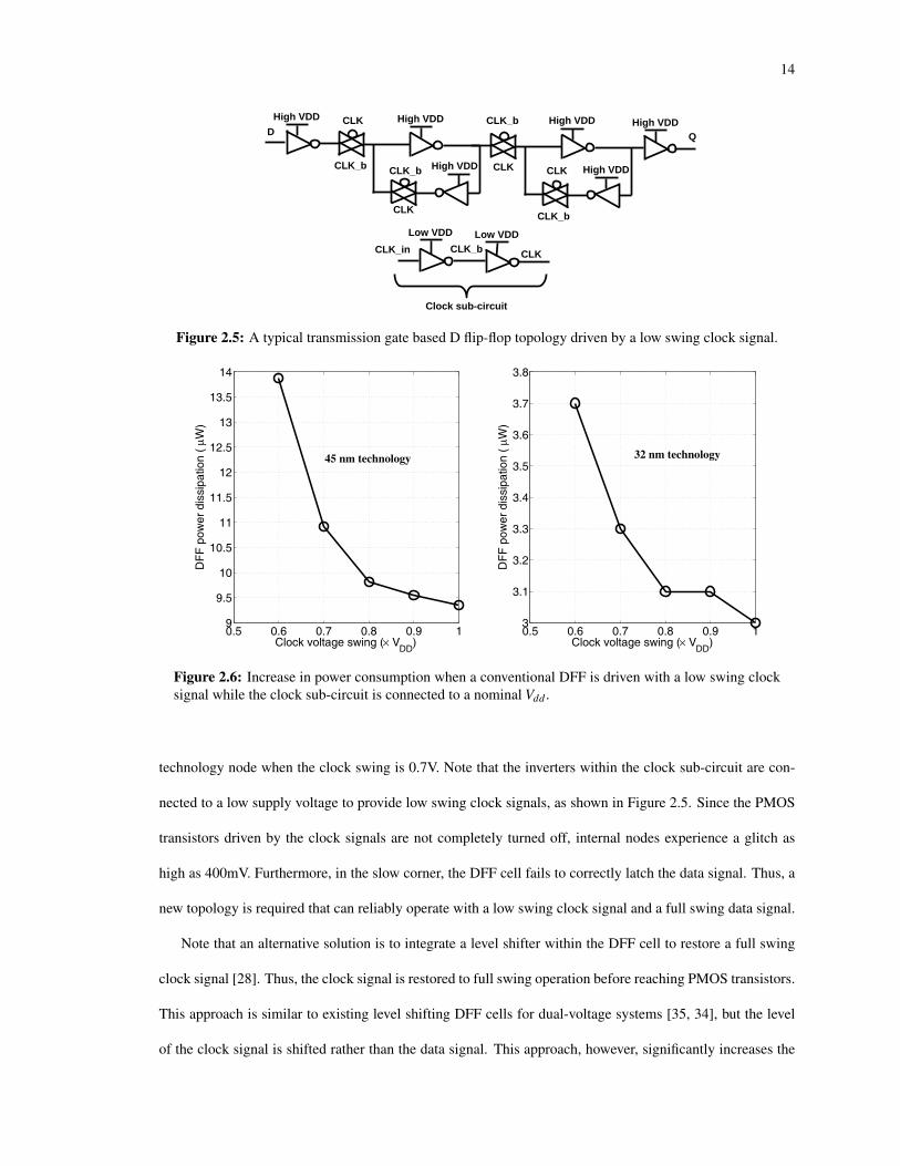
14
1
D Q
CLK_in CLK_b CLK
CLK
CLK_b
CLK_b
CLK
CLK
CLK_b CLK_b
CLK
Low VDD Low VDD
High VDD
High VDD
High VDD
High VDD
High VDD High VDD
Clock sub-circuit
Figure 2.5: A typical transmission gate based D flip-flop topology driven by a low swing clock signal.
0.5 0.6 0.7 0.8 0.9 19
9.5
10
10.5
11
11.5
12
12.5
13
13.5
14
Clock voltage swing ( VDD
)
DF
F p
ower
dis
sipa
tion
( W
)
0.5 0.6 0.7 0.8 0.9 13
3.1
3.2
3.3
3.4
3.5
3.6
3.7
3.8
Clock voltage swing ( VDD
)
DF
F p
ower
dis
sipa
tion
( W
)
45 nm technology 32 nm technology
Figure 2.6: Increase in power consumption when a conventional DFF is driven with a low swing clocksignal while the clock sub-circuit is connected to a nominal Vdd .
technology node when the clock swing is 0.7V. Note that the inverters within the clock sub-circuit are con-
nected to a low supply voltage to provide low swing clock signals, as shown in Figure 2.5. Since the PMOS
transistors driven by the clock signals are not completely turned off, internal nodes experience a glitch as
high as 400mV. Furthermore, in the slow corner, the DFF cell fails to correctly latch the data signal. Thus, a
new topology is required that can reliably operate with a low swing clock signal and a full swing data signal.
Note that an alternative solution is to integrate a level shifter within the DFF cell to restore a full swing
clock signal [28]. Thus, the clock signal is restored to full swing operation before reaching PMOS transistors.
This approach is similar to existing level shifting DFF cells for dual-voltage systems [35, 34], but the level
of the clock signal is shifted rather than the data signal. This approach, however, significantly increases the

15
overall power consumption of the DFF cell due to the integrated level shifter. Thus, the power saved at the
last stage of the clock network is lost within the DFFs, making this approach impractical for the primary
objective of this work.
A conventional flip-flop designed for a full swing clock signal suffers from a prohibiting trade-off between
reliability and power consumption. The reliability issue may cause the flip-flop to latch a wrong data due to
large spikes, which is exacerbated in corner cases. Alternatively, the increase in power consumption is not
tolerable since it conflicts with the primary purpose of this study. It is concluded here that low swing-aware
flip-flop cells are necessary to implement high performance low swing clocking.
Given a low swing-aware flip-flop, the implications of low swing clocking on the clock tree needs to be
re-visited. To this end, implications on timing performance (clock skew and slew) and power consumption of
clock trees with the presence of a low swing-aware flip-flop are presented. Note that the TTS definition is not
necessary in this implementation as the clock pin of the flip-flops are low swing-aware, and the clock slew is
measured from 10% to 90% of low swing level.
In order to investigate the implications of voltage scaling on timing and power characteristics, a sample
clock tree is synthesized for the largest circuit (s35932) of ISCAS’89 benchmarks. Four different cases are
generated by combining two interconnect technologies (wire 1 [59]: R=2Ω/µm, C=0.1fF/µm and wire 2 [37]:
R=8Ω/µm, C=0.2fF/µm) with two frequency/slew constraints:
• Case 1: Wire 1, 1 GHz, 150ps slew constraint,
• Case 2: Wire 2, 1 GHz, 150ps slew constraint,
• Case 3: Wire 1, 1.5 GHz, 100ps slew constraint,
• Case 4: Wire 2, 1.5 GHz, 100ps slew constraint.
The experiments are performed at the slowest PVT corner of two transistor technologies (SS, 0.95V, 125C
for 32nm SAED [59] and SS, 0.9 V, 125C for 45nm FreePDK [38]). The power supply voltage is scaled to
65% of the nominal value with 5% decrements to observe the effect of voltage scaling.
The effect of voltage scaling on clock skew is shown in Figure 2.7(a) and Figure 2.7(b). According
to Figure 2.7(a), in 45nm technology, clock skew slightly increases when the clock voltage is scaled. The

16
(a) Clock skew profile of s35932 with low swing clocking atvarious voltage levels in 45nm technology.
(b) Clock skew profile of s35932 with low swing clocking atvarious voltage levels in 32nm technology.
Figure 2.7: Clock skew profile of s35932.
increase in clock skew does not introduce a violation, assuming a 50ps skew constraint. In 32nm technology,
however, clock skew increases as clock voltage is reduced, reaching and even exceeding the skew constraint,
as shown in Figure 2.7(b). This violation can be fixed with a post-CTS optimization, however, a more
challenging issue in low swing clocking is the significant increase in clock slew, as described below.
Lower voltage degrades the drive ability of clock buffers, which significantly increases clock slew, partic-
ularly in nanoscale technologies where interconnect resistance is dominant. This deleterious effect is depicted
in Figure 2.8(a) and Figure 2.8(b) for, respectively, 45nm and 32nm technologies. According to these figures,
in low swing operation, clock slew increases by approximately 50% in 45nm technology, and approximately
100% in 32nm technology. Note that the same slew constraint as in full swing clocking can be satisfied at low
swing operation through buffering the existing topology. This approach, however, causes significant power
dissipation due to the necessity of high number of clock buffers to satisfy the slew constraint at each clock
sink. Furthermore, the increase in the number of clock buffers increases the insertion delay of clock tree,
potentially increasing the clock skew more than what is shown in Figure 2.7(a) and Figure 2.7(b). Due these
reasons and the failure to efficiently fix these violations through buffering, it is concluded here that a low
swing-aware re-synthesis is required.

17
(a) Clock slew profile of s35932 with low swing clocking atvarious voltage levels in 45nm technology.
(b) Clock slew profile of s35932 with low swing clocking atvarious voltage levels in 32nm technology.
Figure 2.8: Clock slew profile of s35932.
The effect of clock voltage on power consumption is investigated when the clock tree is re-synthesized
to satisfy both skew and slew constraints. The power consumption of the clock tree (clock buffers and
interconnects) at each voltage level is shown in Figure 2.9(a) and Figure 2.9(b) for, respectively, 45nm and
32nm technologies. Note that the lowest voltage in the graphs represent the minimum achievable voltage
without introducing any slew violations. According to Figure 2.9(a), for 45nm technology, at 100ps slew
constraint using wire 1, the power savings reach a maximum of approximately 33% when the clock swing
is at 75% of Vdd . Note that no feasible clock tree can be synthesized for 100ps slew constraint case using
wire 2. Thus, this case is omitted in the figure. At 150ps slew constraint using wire 1, the power savings
reach approximately 46% when the clock swing is at 65% of Vdd . Alternatively, at 150ps slew constraint
using wire 2, power savings reach approximately 44% when clock swing is at 75% of Vdd . According to
Figure 2.9(b), for 32nm technology at 100ps slew constraint, the power savings are approximately 6% when
the clock swing is at 90% and 95% of Vdd for, respectively, wire 1 and wire 2. For the 150ps slew constraint,
the power savings reach approximately 18% (when the clock swing is at 75% of Vdd) and 24% (when the
clock swing is at 80% of Vdd) for, respectively, wire 1 and wire 2.
As shown in Figure 2.9(a) and Figure 2.9(b), the minimum achievable clock swing varies depending
upon the interconnect technology (wire 1 versus wire 2) and the slew constraint. Furthermore, according to

18
(a) Clock tree (clock buffers and interconnects) power con-sumption profile of s35932 at various clock swings in 45nmtechnology.
(b) Clock tree (clock buffers and interconnects) power con-sumption profile of s35932 at various clock swings in 32nmtechnology.
Figure 2.9: Clock tree (clock buffers and interconnects) power consumption profile of s35932.
this experimental setup, depending upon the specific case (as described above), power savings vary between
approximately 6% up to approximately 46%. Thus, a slew-aware clock tree synthesis methodology is required
to efficiently use the resources at different interconnect and transistor technologies, and clock frequencies.
If this condition is satisfied, significant reduction in power can be achieved while also satisfying the same
timing constraints. Thus, significant reduction in power consumption is possible without degrading circuit
performance.
2.1.4 Low Swing Clocking in FinFET Technology
In sub-32nm technologies, FinFETs have emerged as a promising alternative to planar CMOS technology, as
it has smaller device delay and significantly low leakage current, thanks to its enhanced electrostatic control
of the transistor channel [10]. Although clock slew is still an important challenge for FinFET-based ICs,
its enhanced delay and leakage power properties provide additional benefits for low swing clocking. In
this subsection, the implications of low swing clocking on clock skew and power consumption are analyzed
thoroughly with comparisons between typical 32nm planar CMOS and 20nm FinFET technologies.
Although the insertion delay itself is not a design specification, higher insertion delay causes high clock
skew. Thus, minimizing the clock insertion delay is one of the design objectives. The insertion delay in-
19
creases when the clock swing (magnitude) is decreased, as presented in Chapter 2.1.3. On the other hand,
the gate delays in the FinFET technology are negligibly low, particularly when compared to the delays of the
interconnects. As such, the effect of low supply voltage on the gate/buffer delay must be re-considered and
compared against the planar CMOS technology.
In order to highlight this phenomenon, the insertion delays of a full swing and a low swing clock tree for
the 20nm FinFET and 32nm planar CMOS technologies are compared on s38584 of ISCAS’89 benchmarks.
20nm FinFET models are obtained from PTM models [47], and 32nm planar CMOS models are obtained
from SAED 32nm library of Synopsys [59], both of which are simulated using HSPICE of Synopsys. One
clock tree is synthesized at each technology so as to have similar insertion delays at full swing. These clock
trees are simulated at the full swing (Vdd) and the low swing (0.7×Vdd) in order to observe the respective
changes in the insertion delay. The insertion delay of each clock sink in s38584 is presented by normalizing
them to their full swing delays in Figure 2.10 from 100% of Vdd to 70% of Vdd with 5% decrements. It is
shown that the insertion delay of a clock sink in 32nm planar CMOS technology increases by approximately
120% whereas this increase is approximately 26% for the 20nm FinFET technology when clock voltage swing
is scaled down to 0.7×Vdd . In order to analyze the effect of the increase in insertion delay on clock skew, the
minimum and the maximum insertion delays, and the clock skew of FinFET-based and planar CMOS-based
clock trees at full swing and low swing operations are presented in Table 2.1. It is shown that the clock skew
increases severely in the low swing operation of 32nm planar CMOS (to 55.5ps, from 29.4ps at full swing),
compared to the increase in 20nm FinFET (to 29.3ps, from 22.2ps at full swing), even when the FinFET and
planar CMOS technologies have similar insertion delays at the full swing operation. This example shows the
superiority of FinFET technology over its counterpart in planar CMOS technology, by having small timing
sensitivity against a change in the supply voltage. With this observation, it is concluded here that FinFET
technology inherently improves one significant aspect of low swing trees (i.e. clock skew) by providing a low
insertion delay.

20
Figure 2.10: Insertion delay characteristic of 20nm FinFET and 32nm planar CMOS technologies atdifferent voltage levels interpolated from 100% to 70% of Vdd with 5% decrements.
Table 2.1: The comparison of full swing and low swing insertion delay characteristics at 20nm FinFETand 32nm planar CMOS technologies for s38584.
20nm FinFET 32nm planar CMOSMinimum Insertion Delay when CLK @Vdd (ps) 198.0 194.5Maximum Insertion Delay when CLK @Vdd (ps) 220.2 223.8Clock Skew when CLK @Vdd (ps) 22.2 29.3Minimum Insertion Delay when CLK @0.7×Vdd (ps) 250.0 419.3Maximum Insertion Delay when CLK @0.7×Vdd (ps) 279.4 474.8Clock Skew when CLK @0.7×Vdd (ps) 29.4 55.5
As for power consumption, the power consumption of a clock tree can be divided into 2 parts: Dynamic
and static (leakage) power consumption. The dynamic power consumption is formulated as:
Pdyn = αCtotal fV 2swing (2.4)
where α is the switching factor, f is the operating frequency and Vswing is the supply voltage of the clock
buffers. The total capacitance Ctotal is:
Ctotal = ∑∀i
Cbu f f eri +∑
∀ jCsink
j +∑ l× cunit (2.5)
with a design which has i clock buffers with an input capacitance of Cbu f f eri , j sinks with an input capacitance

21
of Csinkj , and a per-unit interconnect capacitance of cunit . Note that short-circuit power is neglected since
transition times are sufficiently small due to tight slew constraints. The low swing clock trees target to save
substantial (quadratic) dynamic power by scaling clock swing [Vswing in Eq. (2.4)]. For instance, a 30% drop
off from the full swing clock swing can lead to 51% savings in the dynamic power dissipation. However,
it is also important here to note that the number of clock buffers needs to be increased to satisfy the same
timing constraints in low swing operation as the full swing operation. This increase in the number of clock
buffers sacrifices some of the power savings obtained through Vswing scaling by increasing Ctotal . Thus, it is
concluded here that a high performance low swing clock tree design methodology should efficiently place
clock buffers in order to satisfy the same performance (timing) constraints as the full swing clock tree, while
minimally trading off the dynamic power savings by minimizing the increase in Ctotal .
Given a FinFET-based clock buffer library, the static (leakage) power consumption depends on the number
of clock buffers:
Pstatic ≈∑∀i
Pbu f f erileakage (2.6)
Thus, minimizing the number of clock buffers i for capacitance-induced dynamic power minimization op-
portunistically minimizes the static power consumption of the FinFET-based buffers. Furthermore, lowering
the Vdd level on the clock tree also decreases the leakage due to the lower electrical field on the transistor
channels. In order to highlight the low leakage property of FinFET technology compared to its counterpart in
planar CMOS technology, two clock trees are synthesized for s38584 of ISCAS’89 benchmarks, using 20nm
FinFET [47] and 32nm planar CMOS [59] libraries. The leakage power comparison of the two technologies
is presented in Table 2.2. It is shown that the leakage power consumption in FinFET decreases significantly
compared to planar CMOS technology. In the full swing implementation, the leakage power decreases to
15.3µW from 319.5µW. In low swing operation, the leakage power in planar CMOS technology decreases to
92.5µW, however it is still ≈7× as large as its FinFET counterpart.
2.1.5 Low Swing Clocking in Gated Clock Trees
The effects of low voltage operation on timing and power trends of gated clock trees are presented in this
subsection. When the clock voltage is scaled for low voltage operation, , the power consumption of the clock

22
Table 2.2: The leakage power consumption comparison of low swing and full swing implementationsof clock trees built on s38584, in 20nm FinFET and 32nm planar CMOS technologies.
CLK Level 20nm FinFET (µW) 32nm planar CMOS (µW)Full Swing (Vdd) 15.3 319.5Low Swing (0.7×Vdd) 13.1 92.5
Figure 2.11: Clock skew and clock slew profile of s35932 at various voltage levels. Although the clockskew and slew constraints (50ps and 100ps, respectively) are satisfied at nominal Vdd , violations occurat low voltage operation.
buffers decreases while the delay and the output slew of the clock buffers increase, as shown in Chapter 2.1.3.
The same is true for the integrated clock gating (ICG) cells. Similar to Chapter 2.1.3, the respective increases
in the output slew of buffers and clock gates accumulate through (e.g. clock branch) interconnects potentially
causing slew violations. Inserting additional buffers in order to avoid slew violations results in higher power
consumption, degrading the power savings obtained through low voltage clocking.
In order to investigate this trade-off, two clock tree cases for s35932 of ISCAS’89 benchmarks are con-
sidered as follows:
1. a gated clock tree is synthesized once at nominal Vdd , and its timing characteristics are observed at
lower voltage levels, allowing slew violations at low voltage operation,
2. a gated clock tree is re-synthesized at various voltage levels to satisfy the slew constraint.

23
Figure 2.12: Power consumption comparison of cases 1 and 2, when normalized to the power consump-tion at nominal Vdd .
These two cases are generated using 45nm technology [38] at 1.5 GHz while clock voltage is scaled from
100% to 70% of its nominal value (0.9V for this technology) with 5% decrements. In order to demonstrate
the timing degradation in case 1, its clock skew and clock slew are plotted at different voltage levels, and
shown in Figure 2.11. It is shown that voltage scaling on the clock tree results in clock skew and clock slew
violations even when these timing constraints (50ps for skew, and 100ps for slew) are satisfied at the nominal
voltage level. Thus, re-synthesis of gated clock trees are necessary, as in case 2. In order to demonstrate the
degradation in power savings while addressing the clock skew and clock slew challenges (to avoid violations),
the power consumption of case 1 and case 2 are compared in Figure 2.12. It is shown that power consumption
decreases significantly when the clock voltage is scaled down without a re-synthesis (with slew violations,
case 1) whereas the power savings start leveling after some point due to additional buffers inserted to satisfy
the slew constraint when clock trees are re-synthesized (case 2), similar to the outcome of Chapter 2.1.3.
2.2 Multi-Voltage Single-Clock Domain Clock Distribution Networks
Multi-voltage single-clock domain designs necessitate the use of different clocking techniques due to the
following challenges: 1) the insertion delay increases in lower voltage domains, requiring a delay insertion
in higher voltage domains to bound clock skew, and 2) level shifting (high-to-low or low-to-high) of clock

24
Figure 2.13: Typical multi-voltage clock tree topology presented in [62].
voltage swing is necessary for cross domain clock delivery. In addition to these challenges, additional buffer
insertion is necessary to satisfy slew constraints, as explained in Chapter 2.1. The power overheads of buffer
and level shifter cell insertion need to be analyzed against the power savings obtained through multi-voltage
design.
The implications of multi-voltage clocking on the clock tree and clock mesh topologies are presented
in Chapter 2.2.1 and Chapter 2.2.2, respectively. The effect of PVT variations on multi-voltage clocking is
presented in Chapter 2.2.3.
2.2.1 Multi-Voltage Clocking with Clock Tree Topology
Due to its easy integration into multi-voltage domain designs, multi-voltage clocking with a tree topology is a
popular technique with sophisticated automation techniques existent in industrial tool flows [62, 63]. Multi-
voltage clock trees are designed to deliver clock signal with local trees in each voltage domain and these trees
are connected at the upper level through level shifters, as shown in Figure 2.13 [62].
Multi-voltage clock tree topology is a power-efficient method of implementing multi-voltage clocking,
yet it has challenges to satisfy timing constraints. Clock tree topology is intolerant to PVT variations, which
exacerbates in the multi-voltage designs due to different timing characteristics of different voltage domains
at multiple PVT corners.

25
c
Premesh Tree
Premesh Drivers
Clock Source
(a) Typical single-voltage domain clock mesh topology.
c c
Clock Source
Premesh Trees
Premesh Drivers
LS
(b) Multi-voltage domain clock mesh topology.
Figure 2.14: Clock mesh topologies.
2.2.2 Multi-Voltage Clocking with Clock Mesh Topology
In the presence of PVT variations, clock mesh topology, shown in Figure 2.14, is a promising alternative.
Compared to clock tree topology, typical single-voltage clock mesh topology [shown in Figure 2.14(a)]
achieves low clock skew, and provides tolerance against PVT variations, thanks to the short circuit con-
nection of clock mesh wires balancing delay mismatches (i.e. clock skew) at the last level. However, de-
creasing the skew across multiple pre-mesh trees is a challenge for multi-voltage meshes as the pre-mesh
trees depicted in Figure 2.14(b) are isolated, and isolated clock meshes across voltage domains do not have
a short circuit connection. Clock skew within each domain can be reduced by using dense meshes for both
single-voltage [Figure 2.14(a)] and multi-voltage cases [Figure 2.14(b)]. However, this improvement in tim-
ing performance is enabled by trading off power consumption, as additional capacitance introduced by clock
mesh wires introduce additional power consumption, compared to the tree topology.
2.2.3 Effect of PVT Variations in Multi-Voltage Clocking
Multi-voltage clocking algorithms have the following challenges: First, gate delay changes with the change
of its supply voltage. Second, the variation in the gate delay is not the same for the identical gates when
they operate at different voltage levels. Clock skew is defined as the difference between the maximum and
the minimum insertion delays, which may fall on different branches within separate voltage domains. To
this end, the insertion delay profile of clock trees need to be carefully investigated to optimize clock skew.
This investigation also reveals how to design pre-mesh tree branches of clock meshes within separate voltage
domains in the presence of PVT variations of multiple corners. In order to analyze how the insertion delay

26
BUF
DFF
DFF
DFF
DFF
DFF
DFF
DFF
DFF
DFF
DFF DFF
DFF
DFF DFF
DFF DFF DFF
DFF DFF
DFF
DFF
DFF DFF
DFF
DFF
DFF
DFF
DFF
DFF DFF
DFF DFF
1.2V domain 0.8V domain
BUF
BUF
BUF
BUF
BUF
BUF
BUF
BUF
BUF
Figure 2.15: Simple two-level clock tree with 16 sinks.
Table 2.3: Insertion delay profile of the motivational clock tree example at two voltage domains shownin Figure 2.15. The maximum and the minimum insertion delays that define the global skew are markedwith bold.
Best (ps) Nom (ps) Worst (ps)Min ins delay in 0.8V D. 104.7 157.8 301.7Max ins delay in 0.8V D. 106.6 161.5 309.6
Inc. compared to Best - ≈ 55 ≈ 203Min ins delay in 1.2V D. 101.4 130.7 223.5Max ins delay in 1.2V D. 101.7 131.3 224.7
Inc. compared to Best - ≈ 30 ≈ 122Global Skew 5.3 30.8 86.1
varies depending on the supply voltage, a motivational example is presented with two voltage domains, each
with a simple two-level clock tree with 16 sinks, as depicted in Figure 2.15.
In this motivational example, one domain is supplied with 1.2V and the other is with 0.8V, and SPICE
models of SAED 90nm EDK library of Synopsys are used [58]. This simple example is synthesized by
IC Compiler of Synopsys using the same size of clock buffers. This circuit is simulated in CustomSim XA
simulator of Synopsys at 500 MHz, and the insertion delay is measured in three different PVT corners: The
best, nominal and the worst cases of the PVT corners. The insertion delay profile is shown in Table 2.3.
It is observed in Table 2.3 that the insertion delay variation is higher in the 0.8V domain which also
increases the skew switching from the best case to the worst case: Maximum insertion delay increases by
approximately 203ps to 309.6ps, whereas the minimum insertion delay only increases by approximately
122ps to 223.5ps. In this undesirable case, the maximum insertion delay increases the largest, as it is affected
by PVT variations the most going from the best to the worst case. The minimum insertion delay, on the other

27
Table 2.4: Improved skew values with a delay insertion to the 1.2V Domain.
Only first level upsized by one Both levels upsized by oneBest (ps) Nom (ps) Worst (ps) Best (ps) Nom (ps) Worst (ps)
Min ins. delay in 0.8V D. 104.6 157.5 301.1 104.6 157.5 301.2Max ins. delay in 0.8V D. 106.5 161.3 308.9 106.6 161.3 309.0Min ins. delay in 1.2V D. 115.2 145.1 239.6 129.9 164.8 269.5Max ins. delay in 1.2V D. 115.5 145.6 240.8 130.0 165.1 270.2Global Skew 10.9 16.2 69.3 25.4 7.6 39.5
hand, increases the least, which is also undesirable. It is desirable, instead, that the maximum insertion delay
path be delayed the least and the minimum insertion delay be delayed the most going from the best to worst
corner, to bound clock skew. The observation here is the fact that the maximum insertion delay path should
be placed in the higher voltage domain at the best case on purpose, as paths in the higher voltage domain has
a higher tolerance to PVT variations, in order to lower the skew budget across all PVT corners.
In order to demonstrate this postulate, the insertion delay of the higher voltage domain is increased grad-
ually by i) upsizing the first level of the two-level motivational clock tree, and ii) upsizing both levels of the
two-level clock tree. It is expected that the insertion delay in higher voltage (1.2V) domain increases by a de-
lay offset in all PVT corners, which may increase the skew in the best case corner, but decrease the skew in the
worst case, therefore, decrease the global skew. The insertion delay profiles of these two cases are presented
in Table 2.4. It is observed that the global skew is decreased when the insertion delay is gradually increased
in the higher voltage (1.2V) domain by upsizing the clock buffers. It is clear that a novel clock network syn-
thesis methodology should control the insertion delay of different voltage domains by either adding/removing
buffers or upsizing/downsizing over a naive, single-corner optimized tree. Notice how the minimum and the
maximum insertion delays (marked in bold) are consistently in the same voltage domain in all three corners
in the undesired case shown in Table 2.3. In the desired case, shown in Table 2.4, the delays vary between
paths in either voltage domains for PVT corners, the skew being affected less from PVT variations. Although
the skew is increased in the best corner (from 5.3ps to 25.4ps), global skew is defined as the worst case of
all corners: Thus, global skew is improved from 86.1ps to 39.5ps, when the insertion delay is shifted by an
upsizing. This example concludes that optimizing clock skew at all three corners simultaneously is possible,
yet it requires a methodical approach to address this challenge.

28
Chapter 3: FEASIBILITY STUDY OF LOW SWING CLOCKING
A novel methodology that implements a low swing clock tree on a legacy clock tree is proposed to show
the feasibility of low swing clocking. For low power IC design, low swing clock trees are one of the known
techniques to lower the overall power dissipation through decreasing the power consumption of the clock
network, while trading off the clock skew, clock slew and local timing (slack). In this chapter, an iterative
skew minimization scheme for low swing clock trees is proposed via in-place buffer sizing on a legacy
full swing clock tree. The proposed approach preserves the power savings of the low swing clock tree
implementation. The effect of the decreased clock swing on the local timing is analyzed: The degradation in
the timing slack is shown to be insignificant due to bounded TTS, eliminating most of the timing degradation
on the clock network or the logic paths induced by decreased clock swing. The experimental results show that
the proposed methodology can achieve an average of up to 11% power savings, with a skew degradation of
less than 5% compared to the original full swing clock tree, satisfying a practical skew budget. The proposed
methodology is highly practical as it only performs in-place buffer sizing on the original clock tree.
3.1 Introduction
Low swing clock trees can be implemented with varying implications at different levels. One previous ap-
proach proposes to use a low swing clock signal over the entire clock tree and convert the signal to full swing
at the sink level using level shifter cells [39]. Another approach introduces a custom flip-flop design, that can
directly be interfaced to a low swing clock signal by minimizing its negative effects on the local timing [20].
Another approach considers to design special buffer cells that can convert the swing of the voltage both full
swing-to-reduced swing (FSRS) and reduced swing-to-full swing (RSFS) in order to isolate full swing clock
source and clock sinks from the low swing clock tree [2]. These approaches of previous studies achieve
promising results, however, the applicability of low swing operation remains limited due to use of specialized
design elements (e.g. low swing level shifters, low swing flip-flops, etc.). If low swing clocking is performed
without the use of such specialized circuit elements, a number of key issues need to be methodically ad-

29
dressed for practical use, including: i) increase in clock skew, ii) degradation in the desired power reduction
due to the need to optimize clock skew, and iii) degradation in the timing slack due to the increase in the
clock slew. In the proposed methodology, a pragmatic approach is adopted to show the feasibility of low
swing clocking. The proposed approach converts a full swing clock tree built by an high quality clock tree
synthesis (CTS) tool to a low swing clock tree. The methodology does not depend on the existence of explic-
itly sized level shifters, or utilize special low swing flip-flop or level-shifting buffer cells, in order to remain
compatible with standard cell libraries in the industry. The proposed flow also keeps the clock skew below
the same practical limit that was used in the design of the original (full swing) clock tree design (issue 1),
preserves the power savings of the low swing implementation (issue 2), and has insignificant degradation in
the local timing (slack) by keeping the clock slew below the same practical limit as the original full swing
clock tree and considering the effect of clock swing scaling (issue 3). The proposed methodology is inte-
grated in its entirety into an industrial tool flow to demonstrate the practicality and short-term applicability
of the proposed novelties in low swing clocking. An automated methodology that synthesizes a low swing
clock network satisfying practical skew and slew constraints is proposed for the first time in this dissertation.
The proposed methodology is not a straight-forward procedure due to the following challenges:
1. the effect of sizing a clock buffer on the insertion delay of clock branches must be characterized as the
timing models of buffer library may not be available at the target low swing voltage level,
2. the effect of a low swing clock on the full (data) swing register sinks must be analyzed, as it has a direct
effect on the local timing (slack),
3. the skew and the slew must be bounded considering multiple PVT corners.
The proposed methodology receives a synthesized full swing clock tree as an input, performs a buffer library
characterization step so as to analyze the effect of upsizing/downsizing of each buffer cell in the library, and
minimizes the clock skew to bound it below a practical limit by sizing clock buffers considering the selected
low swing Vddr . Given these two steps, the proposed flow can target any point on the power vs. skew curve
by assigning the low swing Vddr . The low swing supply voltage Vddr can be provided by one of the following
means, depending on the availability of the voltage levels and the design resources:

30
1. a power grid at the low swing Vddr might already be present, pre-planned for a low-power implementa-
tion of logic,
2. power converters can be placed on an existing power grid to generate the desired low swing Vddr ,
3. an additional power grid can be generated at the desired low swing Vddr .
Given most contemporary designs have high number of clock and voltage domains, it is reasonable to assume
the availability of the voltage level desired for low swing clocking through options 1 or 2 above. The overhead
of the additional grid, if necessary as in option 3, might be prohibitive to the use of low swing clocking.
Assuming options 1 or 2 for the availability of the desired voltage level burdens little to no resources, and the
proposed methodology obtains substantial power savings, while preserving (almost) the same skew of a full
swing clock tree with a reasonable run time.
The rest of the chapter is organized as follows. The key observations that drive the proposed methodology
are introduced and discussed in Chapter 3.2. The proposed methodology of this work is explained in detail in
Chapter 3.3. The results of the performed experiments on benchmark circuits are presented in Chapter 3.4.
The chapter is finalized with concluding remarks in Chapter 3.5.
3.2 Observations on Local Timing
In order to observe the effect of low swing clocking on the local path delay, its relationship to TTS (defined in
Chapter 2.1.2) needs to be studied. However, the timing information for standard cells may not be available
at the selected low swing voltage level Vddr . The necessitated support is the timing data for standard cells at
varying voltage levels of low swing (e.g. 0.85×Vdd , 0.9×Vdd) which may not exist in libraries. Instead, gates
may be characterized only at supported voltage nodes, e.g. 0.8V for low voltage Vdd,low and 1.2V for high
voltage Vdd,high. The static timing analysis tools are not applicable to measure the timing slack (i.e. impact
of TTS) in the absence of these circuit models at different low swing voltage levels in the standard cell
libraries. In order to fill this gap in empirical verification, 20 random paths, which are created using the
available types of flip-flops and logic cells in the target library, are analyzed at 4 different voltage levels
of nominal Vdd (0.95×Vdd , 0.9×Vdd , 0.85×Vdd , 0.8×Vdd). This analysis is performed in order to observe
the relationship between TTS and the degradation in local timing. Naturally, these 20 random paths do not

31
theoretically validate the local timing but are empirically demonstrative of the effectiveness of low swing
clocking in causing only minimal degradation in the timing slack. It is also important to note that, this change
in the voltage level of the clock signal only significantly changes the clock-to-q delay of the flip-flop, and
the delay on the rest of the local timing path (that contributes to slack) is almost unaffected. It is noted here
that despite operating with low swing clocking, the slew of the flip-flop output is not degrading significantly,
as the combinational delay in the local timing path is not degrading in a measurable rate (< 1ps). Thus, it
is sufficient to analyze the relationship between TTS and the clock-to-q delay of different types of flip-flops
in the library independent of the logic paths in the design. There are four different flip-flops in the selected
90nm SAED Library [58] of Synopsys, therefore it is sufficient to consider 20 random paths.
In this demonstrative example of 20 random paths, 200ps is set as the slew constraint, which is a typical
value (10% of the clock period at 500 MHz operation). The circuit elements on the local data paths (combi-
nation logic and the flip-flops) are supplied by full swing voltage at 1.2V. The clock signal is applied with 4
different voltage levels of low swing, keeping the uniformity of operation with the same 200ps slew in each
low swing operation case.
In this experiment with 20 random paths, the effect of low swing clocking on the local timing are inves-
tigated in order to have a clear understanding of the parameters traded off against each other. The slew, the
measured TTS values, the average increase and the worst case increase in the clock-to-q delay of 20 random
paths at 4 voltage levels with a 200ps slew constraint are shown in Table 3.1. It is empirically confirmed that
the effect of low swing clock signal with a fixed slew has a minimal effect on the local timing. The degrada-
tion in the timing slack is 1.8ps, 3.4ps, 5.6ps and 8.8ps when the voltage swing is set to 95%, 90%, 85% and
80% of the nominal Vdd , respectively. It is also important to note here that the average clock-to-q delay of the
flip-flops at these 20 random cases is measured to be 361.0ps. Thus, degradation in the clock-to-q delay is
less than 2.4% of the nominal clock-to-q delay for all cases. Having gradually decreasing timing slack with a
downscaling low swing voltage level shows that the savings in the power consumption are successfully traded
off with degradation in timing slack (i.e. performance). The worst decrease across 20 random paths is 8.8ps
at 80%, which is insignificant as it is only 0.4% of the clock period.

32
Table 3.1: Measured TTS values, and the effect of a low swing clock supply on the local timing (averageand maximum slack decrease) under the same clock slew. The decreased slack, induced by increasedclock-to-q delay, is traded off for the power savings of low swing clocks.
Slew (ps) TTS (ps) Average Slack Max SlackDecrease (ps) Decrease (ps)
Vdd 200.0 79.7 - -0.95×Vdd 200.0 83.8 1.3 1.80.90×Vdd 200.0 88.5 2.9 3.40.85×Vdd 200.0 93.7 5.1 5.60.80×Vdd 200.0 99.5 7.8 8.8
Obtain TTS values
Construct TTS-based library models
Run Static Timing Analysis for verification
Perform SPICE accurate worst-case analysis on flip-flops
Set slack degradation on all local paths pessimistically for verification
Verified design
Complex & Time Consuming: More accurate
Simple & Fast: Pessimistic, less accurate
Figure 3.1: The two alternatives to verify the local timing (slack). In this methodology, the simple andfast approach (bottom flow) is used to bound the degradation in timing slack with a pessimistic bound.
It is concluded that, the measured TTS values here can be set as a new timing constraint to be used in
the optimization phase of the methodology in lieu of the slew constraint. There are two ways to perform
the verification of local timing (slack), shown in Figure 3.1. The first approach (top flow in Figure 3.1)
is to perform an additional cell characterization study of standard cells, in order to develop timing models
at varying voltage levels Vddr of low swing. This approach is not presented here nor used in experiments,
aiming not to divert the discussion from low swing clock tree design. The second approach (bottom flow in
Figure 3.1) is used in this work. The second approach is to perform a worst-case bound approach, where
SPICE simulations are performed to identify worst case timing values, and these values is imposed on the
timing conservatively.

33
3.3 Methodology
In Chapter 2.1.2, it is shown that substantial power savings can be obtained through low swing clocking with
a degradation in clock skew, and it is verified in Chapter 3.2 that the degradation in local timing (slack) is
insignificant with a bounded TTS. Based on these observations, the proposed design methodology optimizes
the low swing clock trees by:
1. minimizing the skew overhead of low swing clock trees without degrading the power savings and,
2. bounding TTS, so as to obtain clock trees that perform minimal to no different than full swing clock
trees with significant power savings.
The proposed methodology optimizes low swing clock trees generated from a full swing clock tree without
any placement or clock topology changes. The methodology only involves in-place buffer sizing, aiming not
to alter the logic placement or full swing clock tree topology, thus aiming for minimal disturbance of legacy
designs. The proposed methodology has three steps:
1. synthesizing an initial clock tree at full swing (unless there is already a legacy design),
2. performing timing characterization of clock buffers in the target library (unless there are already timing
models at the selected low swing voltage level),
3. applying iterative skew minimization considering time-to-switch (TTS) bounds.
The first step is conditional and not necessary if there is already a legacy design. If the proposed method-
ology is used to perform a low swing CTS, an initial optimal clock tree at full swing is necessary. This initial
CTS can be performed with any industrial tool at the traditional full voltage swing. This CTS creates a clock
tree that is optimized for a number of metrics such as routing congestion, tree depth, etc., therefore, it is a
good starting point for the proposed optimization methodology. The second step is also conditional and not
necessary if timing data exists for the cells at the target low swing voltage level Vddr . Note that, it is sufficient
to perform this characterization once for each voltage level of each buffer library. In order to observe the
effect of in-place buffer sizing, the existing timing data or the output of the buffer characterization step is
used to generate look-up tables, as explained in Chapter 3.3.1. In the third and the only mandatory step of the

34
proposed methodology, the skew minimization for low swing clock tree is performed at the given low swing
voltage Vddr . This iterative skew minimization scheme, which is presented in Chapter 3.3.2, is performed on
the clock tree that is initially synthesized for full swing, in order to decrease the skew under a skew bound
without violating the TTS constraint.
3.3.1 Buffer Characterization
Convex optimization methods for buffer sizing are not always feasible due to highly discrete nature of the
problem. Thus, discrete methods, such as iterative optimization as in the adapted approach of this study, are
necessary. In this step, a look-up table based approach is considered to store the delay characteristics of each
clock buffer in the library. The created look-up tables are used in the following discrete, iterative optimization
step (Chapter 3.3.2). Note that these look-up tables need to be created once for each buffer library, and the
utilization of these look-up tables in optimization step improves run-time profile.
In this step, a discrete set of buffer sizes in the library at a discrete set of candidate low swing voltage levels
are considered. The purpose of the characterization is to investigate the effect of upsizing and downsizing
of each buffer on the gate delay. Upsizing a buffer either increases its delay due to the increased loading
effect (input capacitance) on the previous stage, or decreases its delay due to the improved capability of
driving the next stage. Thus, the upsizing/downsizing characteristic of each buffer should be considered
individually and accurately. In order to create an accurate look-up table, a simple two-level circuit is created
by connecting two buffers and an output capacitance in series, as shown in Figure 3.2. The purpose of
this two-level circuit is to account for both the loading effect of each buffer to its previous stage, and the
effect of driving the load in the fanout cone of each buffer on the delay. When a buffer, e.g. NBUFFX8,
is being characterized, two NBUFFX8 buffers are placed in the two-level circuit with a typical capacitance
value. The typical capacitance value is found using the OPTIMIZE function of HSPICE, considering the
slew constraint. With this configuration, look-up tables that are accurate enough are obtained in order to
guide the following step of the proposed scheme (Chapter 3.3.2). However, sizing one buffer changes the
insertion delay on the neighboring paths as well, which is undesired. In order to limit this effect, the number
of times that a buffer can be upsized or downsized is limited by a factor N, which is specified depending
on the size and the granularity of the buffer library. In order to visualize a typical lookup table, the lookup

35
Level-1 Buffer Level-2 Buffer
Figure 3.2: Two-level model for buffer characterization.
table created for NBUFFX8 of Synopsys SAED 90nm Library [58] with N = 2 at 80% of Vdd is shown in
Table 3.2. The buffer at the first level is fixed at NBUFFX8 (a typical parent), and the buffer at the second
level is upsized/downsized to observe the sizing effect. The typical capacitance for the configuration is found
to be 45fF, using the OPTIMIZE function of HSPICE at a 100ps slew constraint. As shown in the Table 3.2,
downsizing NBUFFX8 to NBUFFX4 increases the path delay, whereas upsizing to NBUFFX16 decreases.
On the other hand, if the buffer is upsized twice to NBUFFX32, the path delay increases drastically. This
example shows the non-regular characteristic of buffer delays and the importance of an accurate look-up
table. A possible inaccuracy of these upsizing/downsizing may result in more number of iterations (i.e. more
number of SPICE simulations) in the following step (Chapter 3.3.2). However, this is not observed in the
experiments, therefore, the proposed buffer characterization step is considered practically sufficient. With N
upsizing and N downsizing, a total of 2N simulations are performed for each buffer, and this characterization
needs to be performed for each buffer in the library. Thus, the complexity of this step is O(Nk), for a library
that contains k different sizes of buffers. The parameter N is directly related to the buffer library size k,
thus, the run time of this step has a quadratic dependence to library size. However, as these simulations are
performed on the simple two-level circuit with a finite number of buffers, the run time of this step is on the
order of seconds.
3.3.2 Iterative Skew Minimization
Iterative skew minimization is the major novel step of the methodology. The objective is to preserve the power
savings of an adapted low swing clock tree with (almost) the same timing performance as the counterpart full
swing tree. To this end, this step of the proposed flow targets to minimize the skew of a low swing clock tree,

36
Table 3.2: A typical lookup table for NBUFFX8 of Synopsys SAED Library at 80% of Vdd . The typicalcapacitance is found to be 45fF at a 100ps slew constraint, using the OPTIMIZE function of HSPICE.The parent buffer (Level-1) is fixed at NBUFFX8, and the child buffer (Level-2) is varied to observe theeffect of sizing on delay.
Level-1 Buffer Level-2 Buffer Delay (ps)(Fixed) (Varied)NBUFFX8 NBUFFX8 249.9NBUFFX8 NBUFFX2 265.8NBUFFX8 NBUFFX4 271.1NBUFFX8 NBUFFX16 239.3NBUFFX8 NBUFFX32 342.2
degrade the power savings as minimally as possible and satisfy TTS constraint (defined in Chapter 2.1.2) by
performing an in-place buffer sizing scheme with the guidance of the look-up tables created in Chapter 3.3.1.
The algorithm is presented in Algorithm 1.
In this algorithm, the flip-flop clusters driven by the same clock buffer at the nth level are identified,
and they are considered to have identical insertion delay as they are connected to the same net, where delay
difference is less than 1ps. In order to identify the clusters on which sizing is necessary, an initial SPICE
simulation is performed (Line 2) to obtain the complete insertion delay range of all clusters (whose maximum
and minimum values define the skew). In order to obtain a bounded skew, the range should lie in a permissible
window (where the difference between the maximum and the minimum satisfies the skew constraint). The
clusters which are at either the minimum or the maximum side of the range are marked depending on how
much improvement would be achieved if their insertion delay is moved into the permissible window of
insertion delays (Line 8). By identifying clusters from both ends of the range, it is expected that the number
of buffers to be sized is minimized and the process of obtaining the permissible window is more flexible.
The clusters identified at these ends of the range are marked one at a time and pushed into an either max
or min queue, and dropped from insertion delay range (Lines 9-10). This operation continues until the
unmarked portion of the insertion delay range satisfies the skew constraint skewconst (i.e. the difference
between the maximum and the minimum insertion delay paths on the unmarked portion skewcurr should
be less than skewconst ). At this point, it is assumed that sizing the buffers of the marked clusters (e.g. in
the min and max queues waiting for their insertion delays to be resized into the permissible window) place

37
Algorithm 1 Iterative Skew MinimizationInput: Initial full swing clock tree, low swing voltage level Vddr , timing characterization information of
buffer library, skew constraint skewconst and skew margin skewmargin.Output: New buffer sizes.
1: Selected Buffers Queues, Qmax = Qmin = /0
2: Measure the initial skew, skewmeas3: while skewmeas > skewconst + skewmargin do4: skewcurr = skewmeas5: while skewcurr > skewconst do6: Find buffer Bmin, driving min ins. delay cluster7: Find buffer Bmax, driving max ins. delay cluster8: Select the buffer, which when removed, improves the skew the most, set empty set for the other9: Qmax = Qmax∪Bmax
10: Qmin = Qmin∪Bmin11: Update skewcurr with the remaining set12: end while13: while Qmax! = /0 do14: Pop one buffer, analyze its neighboring buffers15: if neighboring buffers have the same delay profile then16: Size their parent buffer17: else18: Size only the corresponding buffer19: end if20: end while21: while Qmin! = /0 do22: Pop one buffer, analyze its neighboring buffers23: if neighboring buffers have the same delay profile then24: Size their parent buffer25: else26: Size only the corresponding buffer27: end if28: end while29: Run SPICE to measure skewmeas and T T Smeas30: if T T Smeas > T T Sconst then31: Resize the violating branch32: end if33: end while
their insertion delays in the permissible window, and the skew constraint is satisfied at the end of the sizing
phase. After identifying the clusters whose buffers need to be sized, the sizing stage starts. In this stage, the
buffers are popped from the queue one at a time, and its neighboring clusters, the register clusters which are
driven by the same parent buffer at the (n− 1)st level, are investigated (lines 13-20 and 21-28). From the
experiments, it is observed that most clusters that share the same parent at the (n− 1)st level have similar
insertion delay characteristics. If such a case is identified, only this single buffer at the (n− 1)st level is
sized instead of the multiple children at the nth level. This sizing is performed with the guidance of the

38
look-up table from Chapter 3.3.1 for timing purposes (line 16 and 24). The observation to size the parent
buffer instead of multiple children is key with the proposed buffer sizing scheme, because by sizing only one
buffer, the insertion delays of multiple clusters can be moved into the permissible window. If this is not the
case (which is rarely seen in the experiments as industrial CTS tools scrupulously maximize common paths
in neighboring clock branches) only the driving buffer of the corresponding cluster at nth level is sized (lines
18 and 26). This operation is repeated until both max and min queues are empty. At this stage, a final SPICE
simulation is performed to verify that the skew is within the acceptable margin (skewconst + skewmargin), and
the TTS constraint is satisfied (Line 29). If the TTS constraint is violated at a branch, that branch is resized
back to its original. However, it is not encountered in the experiments, as the number of times a buffer
can be sized is limited (by N defined in Chapter 3.3.1). Furthermore, as the buffer sizing is performed
assuming the rest of the network would not be significantly affected, the simulation in this step is vital
to verify that assumption. If the assumption is incorrect, implying that the measured skew is not within
the acceptable margin (skewconst + skewmargin), another iteration is performed. Design-specific parameter
skewmargin is a user-specified acceptable degradation margin for the clock skew, which is set depending on
the performance and run time requirements. For instance, in the experiments, skewmargin is set to 10% of the
skew constraint (0.1×skewconst ). A higher skewmargin would lower the performance with a higher skew but
converge faster, whereas a lower skewmargin would generate a tighter design at the expense of more number
of iterations (i.e. higher run time).
This algorithm is performed at the worst case corner by default, because the highest skew would likely
occur at that corner, and should be bounded. However, the state-of-the-art circuits may have more complex
corners rather than nominal, best and worst, and the largest skew may not occur at the worst case corner.
In order to address that, a multi-corner compatibility verification step is added to preserve the multi-corner-
aware approach of the proposed work. In this second algorithm (Algorithm 2), the worst case corner selected
initially (Line 1) and Algorithm 1 is run (Line 3). In the next step, SPICE accurate simulations are performed
at all corners but the worst case corner to verify the skew bound (Line 4). If the verification fails, the corner
that has the highest skew is set to be the active corner (Line 8), and another iteration of Algorithm 2 is run.

39
Algorithm 2 Multi-Corner Verification1: Set active corner as worst corner2: while TRUE do3: Run Algorithm 14: Verify the skew bound at all PVT corners5: if verified then6: break7: else8: Set active corner as the corner with the largest skew9: end if
10: end while
3.4 Experimental Analysis
3.4.1 Simulation Setup
The proposed methodology is implemented with Tcl in order to inter-operate with the existing industrial
tools (e.g. Synopsys in this case) and tested on 3 largest circuits of ISCAS’89 benchmarks (s35932, s38417,
s38584) and one more benchmark circuit that is created (and called b1) by combining s35932 and s38584.
The combination is performed by combining the netlists of those two circuits, and place them in the same
floorplan. The purpose here is to investigate the quality of results on relatively larger circuits (i.e. with more
number of sinks), and show the scalability of the proposed methodology. Note that ISPD’10 clock contest
benchmarks cannot be used in this analysis, as they do not have (the logic) data to complete the analysis
in the Synopsys flow. Nonetheless, the largest ISCAS’89 benchmark circuit (s35932) has a similar number
of register sinks as that in the largest ISPD’10 clock contest benchmarks (and even higher with the created
b1). The RTL netlists are synthesized using Design Compiler of Synopsys, the physical placement and the
synthesis of the initial full swing clock tree is performed with IC Compiler of Synopsys. The power and the
skew analyses are performed using CustomSim XA simulator of Synopsys at the SPICE accuracy in 90nm
technology [58] operating at 500 MHz. The allowed number of buffer sizings N is set to 2, considering the
number of available buffer sizes is five in the selected SAED 90nm EDK Library of Synopsys. The allowed
degradation margin skewmargin is set to 10% of the skew at the original full swing clock tree, totaling a skew
budget of 1.1× skewconst . At each voltage level, the time-to-switch (TTS) constraint is set to the values found
in Table 3.1, not to degrade the timing slack more than the measured values (8.8ps at the worst case). In order

40
to account for the PVT variations, the optimization is performed at the worst case corner, and the final circuit
is verified at three different PVT corners, which are:
1. Best Corner (BC): V=1.1×Vdd , T=-40C, fast transistors (FF).
2. Nominal Corner (NC): V=Vdd , T=25C, typical transistors (TT).
3. Worst Corner (WC): V=0.9×Vdd , T=125C, slow transistors (SS).
3.4.2 Results
In order to show the effectiveness of the proposed methodology, the skew, the TTS and the power consumption
of the full swing clock tree synthesized by IC Compiler, the low swing clock tree before optimization and the
low swing clock tree after proposed optimization scheme are compared. The experimental results at voltage
levels of 0.90×Vdd , 0.85×Vdd and 0.80×Vdd are shown in Table 3.3, Table 3.4 and Table 3.5, respectively.
At 0.95×Vdd case, the power savings is at 4% with less than 10% degradation in skew, which is already within
the acceptable skew margin before the optimization. Thus, no optimization is performed for that case, and the
comparisons are not reported. The experimental results show that the proposed methodology is applicable
at all available voltage levels in order to obtain skew values as low as the corresponding full swing clock
tree while preserving the substantial decrease in the power consumption: The circuits running at 0.9×Vdd
operate with 8% power savings with no skew degradation, the circuits running at 0.85×Vdd operate with 11%
power savings with 5% skew degradation, the circuits running at 0.8×Vdd operate with 11% power savings
with 2% skew degradation. The decrease in power consumption is achieved through the degradation in the
slew, however the TTS constraint defined in Chapter 3.2 is satisfied at all voltage levels, which guarantees
an insignificant decrease in the timing slack (at 80% of supply voltage, 11% power savings obtained with a
slack decrease of ≈ 8ps, as shown in Table 3.1). Furthermore, it is also important to note that, the proposed
methodology can obtain different power savings (8% to 11%) and different slack degradation (3.4ps to 8.8ps,
as shown in Table 3.1) at different low swing voltage levels varying from 90% to 80% of Vdd , with (almost)
the same skew (at most 5% increase on average) within the budget (1.1× skewconst ). Thus, the proposed
methodology can target a wide range of applications by changing the applied low swing voltage level in order
to budget the available timing slack for power savings.
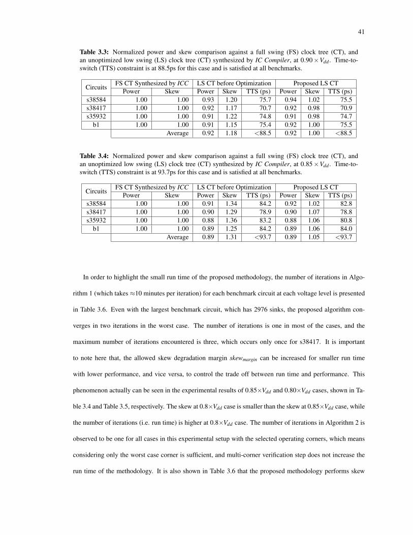
41
Table 3.3: Normalized power and skew comparison against a full swing (FS) clock tree (CT), andan unoptimized low swing (LS) clock tree (CT) synthesized by IC Compiler, at 0.90×Vdd . Time-to-switch (TTS) constraint is at 88.5ps for this case and is satisfied at all benchmarks.
Circuits FS CT Synthesized by ICC LS CT before Optimization Proposed LS CTPower Skew Power Skew TTS (ps) Power Skew TTS (ps)
s38584 1.00 1.00 0.93 1.20 75.7 0.94 1.02 75.5s38417 1.00 1.00 0.92 1.17 70.7 0.92 0.98 70.9s35932 1.00 1.00 0.91 1.22 74.8 0.91 0.98 74.7
b1 1.00 1.00 0.91 1.15 75.4 0.92 1.00 75.5Average 0.92 1.18 <88.5 0.92 1.00 <88.5
Table 3.4: Normalized power and skew comparison against a full swing (FS) clock tree (CT), andan unoptimized low swing (LS) clock tree (CT) synthesized by IC Compiler, at 0.85×Vdd . Time-to-switch (TTS) constraint is at 93.7ps for this case and is satisfied at all benchmarks.
Circuits FS CT Synthesized by ICC LS CT before Optimization Proposed LS CTPower Skew Power Skew TTS (ps) Power Skew TTS (ps)
s38584 1.00 1.00 0.91 1.34 84.2 0.92 1.02 82.8s38417 1.00 1.00 0.90 1.29 78.9 0.90 1.07 78.8s35932 1.00 1.00 0.88 1.36 83.2 0.88 1.06 80.8
b1 1.00 1.00 0.89 1.25 84.2 0.89 1.06 84.0Average 0.89 1.31 <93.7 0.89 1.05 <93.7
In order to highlight the small run time of the proposed methodology, the number of iterations in Algo-
rithm 1 (which takes ≈10 minutes per iteration) for each benchmark circuit at each voltage level is presented
in Table 3.6. Even with the largest benchmark circuit, which has 2976 sinks, the proposed algorithm con-
verges in two iterations in the worst case. The number of iterations is one in most of the cases, and the
maximum number of iterations encountered is three, which occurs only once for s38417. It is important
to note here that, the allowed skew degradation margin skewmargin can be increased for smaller run time
with lower performance, and vice versa, to control the trade off between run time and performance. This
phenomenon actually can be seen in the experimental results of 0.85×Vdd and 0.80×Vdd cases, shown in Ta-
ble 3.4 and Table 3.5, respectively. The skew at 0.8×Vdd case is smaller than the skew at 0.85×Vdd case, while
the number of iterations (i.e. run time) is higher at 0.8×Vdd case. The number of iterations in Algorithm 2 is
observed to be one for all cases in this experimental setup with the selected operating corners, which means
considering only the worst case corner is sufficient, and multi-corner verification step does not increase the
run time of the methodology. It is also shown in Table 3.6 that the proposed methodology performs skew

42
Table 3.5: Normalized power and skew comparison against a full swing (FS) clock tree (CT), andan unoptimized low swing (LS) clock tree (CT) synthesized by IC Compiler, at 0.80×Vdd . Time-to-switch (TTS) constraint is at 99.5ps for this case and is satisfied at all benchmarks.
Circuits FS CT Synthesized by ICC LS CT before Optimization Proposed WorkPower Skew Power Skew TTS (ps) Power Skew TTS (ps)
s38584 1.00 1.00 0.91 1.53 94.9 0.91 1.10 93.6s38417 1.00 1.00 0.89 1.42 89.5 0.89 0.89 89.3s35932 1.00 1.00 0.87 1.52 94.0 0.88 1.09 93.7
b1 1.00 1.00 0.88 1.39 95.2 0.88 0.99 94.9Average 0.89 1.46 <99.5 0.89 1.02 <99.5
Table 3.6: Number of iterations and number of buffers modified for each benchmark circuit at fractionsof Vdd levels.
Circuits Num of Num of Number of Iterations Number of Buffers ModifiedSinks Buffers 0.90× 0.85× 0.80× 0.90× 0.85× 0.80×
s38584 1238 134 1 1 1 1 3 4s38417 1463 150 1 1 3 1 3 2s35932 1728 170 1 2 2 2 3 6
b1 2976 315 1 2 2 3 4 6
minimization efficiently as the number of buffers that are sized (modified) are no more than six (6) among
the 100+ buffers in the clock trees. This is due to the fact that the insertion delay profile of the neighboring
clusters are considered at the buffer sizing stage, and multiple clusters in the region of interest are optimized
with a single sizing at the (n−1)st level.
3.5 Conclusion
In this chapter, a novel optimization scheme is proposed to minimize the clock skew of low swing clock
trees. Low swing clock trees are known to be power efficient, however they have drawbacks in requiring
additional circuitry or suffering from poor performance. This study introduces a fast iterative heuristic to
minimize the skew so as to perform minimal or no different than the full swing clock trees while preserving
power savings of the low swing clock trees. Moreover, it is shown that the low swing clock tree is enabled
with an insignificant degradation in the local timing (slack). The proposed scheme is highly practical, as it
is an added feature in the existing CTS tools with minimal effect on the physical design by only performing
in-place buffer sizing, and without requiring additional circuitry. The trade off between performance and
power consumption can be controlled by varying the applied low swing voltage Vddr on the clock buffers.

43
Furthermore, the trade off between run time and performance can be controlled by varying the allowed skew
degradation margin skewmargin. These features of the proposed scheme makes it highly applicable, as it can
be used for both high performance and low power applications.

44
Chapter 4: DESIGN AUTOMATION FOR LOW SWING CLOCKING
In this chapter, an automated low swing clocking methodology is developed through both circuit and algorith-
mic innovations. The primary objective is to significantly reduce the power consumed by the clock network
while maintaining the circuit performance the same. The methodology consists of two primary components:
1) a novel DFF cell that maximizes power savings by enabling low swing operation throughout the entire
clock network and 2) a novel CTS algorithm to ensure that the same timing constraints (i.e. clock frequency,
skew, and slew) are satisfied. The proposed methodology is integrated within an industrial design flow. Exper-
imental results on ISCAS’89 benchmark circuits demonstrate that the overall power consumed by the clock
tree can be reduced by up to 27% and 44% in, respectively, 32nm and 45nm technologies, while satisfying
the same timing constraints. Furthermore, the proposed low swing DFF cell maintains the clock-to-q delay
the same while achieving up to 32% and 15% power savings in the overall flip-flop power at, respectively,
1 GHz and 1.5 GHz clock frequencies.
4.1 Introduction
Achieving a reliable low swing clock network without sacrificing performance is challenging due to the
following issues: 1) clock buffers operating at a lower voltage increase the insertion delay along the clock
path, causing higher clock skew, 2) the drive ability of the clock buffers is degraded, producing higher clock
slew, and 3) the interface between a low swing clock signal and flip-flop may increase clock-to-q delay,
thereby reducing the timing slack within the data paths while also increasing power consumption. To alleviate
the first two issues, a larger number of clock buffers is required, which sacrifices the power savings. To
alleviate the third issue, a common approach is to restore full swing operation before the clock signal reaches
flip-flops [39, 2]. This approach significantly reduces power savings since the last stage of a clock network
has high switching capacitance.
In this study, these three primary issues are simultaneously addressed through both circuit and algorithmic
innovations, making low swing clocking a practical power reduction strategy for both low power and high

45
Novel Low Swing Clock Tree Synthesis
Clock Buffer Library
Target Skew & Slew
Novel Low Swing DFF Cell
Clock Pin Slew Constraint
Target C2Q delay
Placed Design at Nominal Voltage
Clock Network at Scaled Voltage
Proposed methodology
Figure 4.1: Summary of the proposed methodology to achieve low swing clocking while maintainingthe performance requirements.
performance applications. Furthermore, the proposed methodology is implemented within a standard design
flow for feasible integration into existing automation tools. As depicted in Figure 4.1, the methodology
consists of a novel DFF cell and a novel CTS methodology. The proposed DFF cell enables reliable low
swing operation at the clock sinks while maintaining the timing constraints the same. The proposed CTS
algorithm ensures that the same skew and slew constraints as in full swing operation are satisfied. More
specifically, the proposed methodology has the following characteristics:
1. The proposed low swing DFF cell achieves similar clock-to-q delay as traditional full swing DFF
topology while consuming less power. Reliable operation is ensured despite a low swing clock signal
and a full swing data signal.
2. The proposed slew-aware low swing CTS methodology considers not only capacitance, but also resis-
tance to efficiently utilize clock tree resources at different performance constraints, and target transistor
and interconnect technologies.
3. The increase in the insertion delay due to low swing operation on the clock tree is methodically com-
pensated by embedding a buffer insertion/wire snaking scheme within the CTS for skew minimization.

46
The output of the proposed methodology is a low swing clock tree, running at the same frequency, satisfy-
ing the same clock skew, clock slew constraints as conventional full swing operation, while saving significant
power at both clock tree and DFFs. The proposed methodology is implemented within a conventional IC
design flow, making the methodology highly applicable to automation.
The rest of the chapter is organized as follows. The proposed methodology is described in Chapter 4.2.
Experimental results are presented in Chapter 4.3. Finally, the chapter is concluded in Chapter 4.4.
4.2 Methodology
As shown in Figure 4.1, the proposed methodology consists of a low swing DFF cell and a low swing-aware
CTS algorithm. The proposed low swing DFF cell, presented in Chapter 4.2.1, enables low swing operation
in the clock tree without a power or a delay overhead, even though the logic data signal is at full swing. The
timing modeling of clock buffers and interconnects, presented in Chapter 4.2.2, provides necessary timing
models to the low swing-aware CTS tool. The proposed CTS algorithm, described in Chapter 4.2.3, generates
a low swing clock tree that maximizes the power savings while satisfying the original timing constraints.
4.2.1 Low Swing DFF Design
The proposed DFF topology, depicted in Figure 4.2, is based on the most commonly used, static D flip-flop
shown in Figure 2.5. Rather than using transmission gates, however, pass gates with NMOS transistors (N1,
N2, N5, and N6) are utilized as the switches in both master and slave latches. Thus, when the low swing
clock signal is at logic high, N1 and N6 can completely turn off. Pass gates, however, cannot transfer a full
voltage to the output. This issue is critical since the incoming data signal operates at full swing. Thus, node
A cannot reach a full Vdd , thereby increasing the short-circuit and leakage current in the following stages
in addition to increasing the clock-to-q delay. Furthermore, pass transistors are known to be less robust to
process variations. In order to alleviate these issues, a pull-up network consisting of two PMOS transistors is
added to both master and slave latches (P1 to P4). When the master node M transitions to logic low, P1 turns
on. If the data signal is also at logic low, then node A is pulled to full Vdd through P1 and P2. Note that P2 (in
the master latch) and P4 (in the slave latch) are added to prevent contention current (and therefore reduce
power consumption) when the data signal is at logic high and clock signal is at logic low. In this situation,
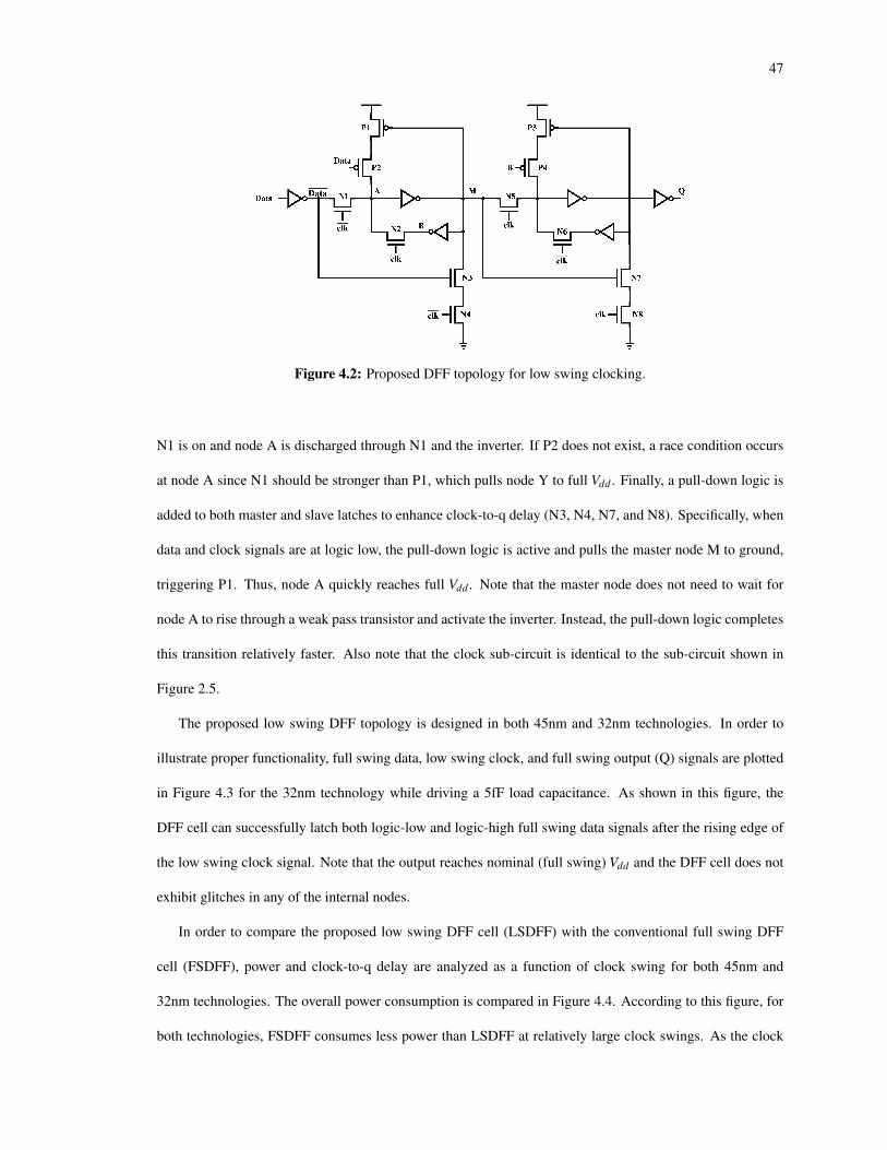
47
Figure 4.2: Proposed DFF topology for low swing clocking.
N1 is on and node A is discharged through N1 and the inverter. If P2 does not exist, a race condition occurs
at node A since N1 should be stronger than P1, which pulls node Y to full Vdd . Finally, a pull-down logic is
added to both master and slave latches to enhance clock-to-q delay (N3, N4, N7, and N8). Specifically, when
data and clock signals are at logic low, the pull-down logic is active and pulls the master node M to ground,
triggering P1. Thus, node A quickly reaches full Vdd . Note that the master node does not need to wait for
node A to rise through a weak pass transistor and activate the inverter. Instead, the pull-down logic completes
this transition relatively faster. Also note that the clock sub-circuit is identical to the sub-circuit shown in
Figure 2.5.
The proposed low swing DFF topology is designed in both 45nm and 32nm technologies. In order to
illustrate proper functionality, full swing data, low swing clock, and full swing output (Q) signals are plotted
in Figure 4.3 for the 32nm technology while driving a 5fF load capacitance. As shown in this figure, the
DFF cell can successfully latch both logic-low and logic-high full swing data signals after the rising edge of
the low swing clock signal. Note that the output reaches nominal (full swing) Vdd and the DFF cell does not
exhibit glitches in any of the internal nodes.
In order to compare the proposed low swing DFF cell (LSDFF) with the conventional full swing DFF
cell (FSDFF), power and clock-to-q delay are analyzed as a function of clock swing for both 45nm and
32nm technologies. The overall power consumption is compared in Figure 4.4. According to this figure, for
both technologies, FSDFF consumes less power than LSDFF at relatively large clock swings. As the clock
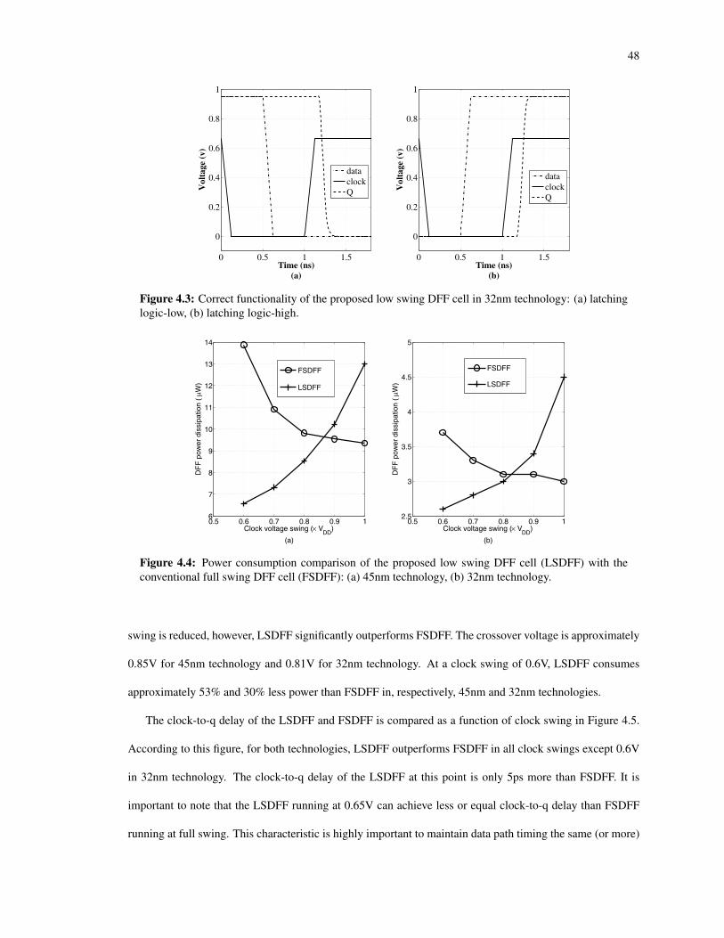
48
0 0.5 1 1.5
0
0.2
0.4
0.6
0.8
1
Time (ns)(a)
Vol
tage
(v)
dataclockQ
0 0.5 1 1.5
0
0.2
0.4
0.6
0.8
1
Time (ns)(b)
Vol
tage
(v)
dataclockQ
Figure 4.3: Correct functionality of the proposed low swing DFF cell in 32nm technology: (a) latchinglogic-low, (b) latching logic-high.
0.5 0.6 0.7 0.8 0.9 16
7
8
9
10
11
12
13
14
Clock voltage swing ( VDD
)
(a)
DF
F p
ower
dis
sipa
tion
( W
)
FSDFF
LSDFF
0.5 0.6 0.7 0.8 0.9 12.5
3
3.5
4
4.5
5
Clock voltage swing ( VDD
)
(b)
DF
F p
ower
dis
sipa
tion
( W
)
FSDFF
LSDFF
Figure 4.4: Power consumption comparison of the proposed low swing DFF cell (LSDFF) with theconventional full swing DFF cell (FSDFF): (a) 45nm technology, (b) 32nm technology.
swing is reduced, however, LSDFF significantly outperforms FSDFF. The crossover voltage is approximately
0.85V for 45nm technology and 0.81V for 32nm technology. At a clock swing of 0.6V, LSDFF consumes
approximately 53% and 30% less power than FSDFF in, respectively, 45nm and 32nm technologies.
The clock-to-q delay of the LSDFF and FSDFF is compared as a function of clock swing in Figure 4.5.
According to this figure, for both technologies, LSDFF outperforms FSDFF in all clock swings except 0.6V
in 32nm technology. The clock-to-q delay of the LSDFF at this point is only 5ps more than FSDFF. It is
important to note that the LSDFF running at 0.65V can achieve less or equal clock-to-q delay than FSDFF
running at full swing. This characteristic is highly important to maintain data path timing the same (or more)

49
0.5 0.6 0.7 0.8 0.9 160
65
70
75
80
85
90
Clock voltage swing ( VDD
)
(a)
DF
F c
lock−
to−
Q d
elay
(ps
)
FSDFF
LSDFF
0.5 0.6 0.7 0.8 0.9 160
65
70
75
80
85
90
95
100
105
Clock voltage swing ( VDD
)
(b)
DF
F c
lock−
to−
Q d
elay
(ps
)
FSDFF
LSDFF
Figure 4.5: Clock-to-q delay comparison of the proposed low swing DFF cell (LSDFF) with the con-ventional full swing DFF cell (FSDFF): (a) 45nm technology, (b) 32nm technology.
Table 4.1: Power-delay product comparison of the proposed LSDFF and conventional FSDFF as afunction of clock swing.
Clock Swing (×Vdd)Power-Delay Product (ps×µW)
45nm 32nmFSDFF LSDFF FSDFF LSDFF
1 769 793 288 2710.9 802 623 298 2080.8 834 526 298 1970.7 940 493 317 2130.6 1241 558 353 270
slack when the conventional flip-flops are replaced with LSDFFs. Finally, power-delay product of the two
flip-flops is listed in Table 4.1, demonstrating the superiority of the proposed LSDFF at each clock swing for
both technologies.
The proposed LSDFF has also been compared in [42] with several existing DFF topologies designed
for low voltage operation such as clocked CMOS and sense amplifier based topology [17], reduced clock
swing flip-flop topology [19], a NAND-type keeper flip-flop topology [61], and contention reduced flip-flop
topology [24]. All of these topologies have been designed to produce a similar clock-to-q delay to achieve
a fair comparison. At a clock swing of 0.7V, the proposed topology achieves, on average, 38.1% and 44.4%
reduction in, respectively, dynamic power and power-delay product while exhibiting similar clock-to-q delay.
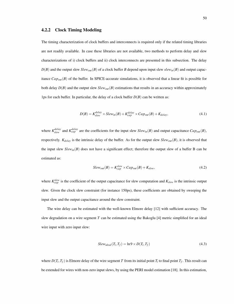
50
4.2.2 Clock Timing Modeling
The timing characterization of clock buffers and interconnects is required only if the related timing libraries
are not readily available. In case these libraries are not available, two methods to perform delay and slew
characterizations of i) clock buffers and ii) clock interconnects are presented in this subsection. The delay
D(B) and the output slew Slewout(B) of a clock buffer B depend upon input slew slewin(B) and output capac-
itance Capout(B) of the buffer. In SPICE-accurate simulations, it is observed that a linear fit is possible for
both delay D(B) and the output slew Slewout(B) estimations that results in an accuracy within approximately
1ps for each buffer. In particular, the delay of a clock buffer D(B) can be written as:
D(B) = Kdelayslew ×Slewin(B)+Kdelay
cap ×Capout(B)+Kdelay, (4.1)
where Kdelayslew and Kdelay
cap are the coefficients for the input slew Slewin(B) and output capacitance Capout(B),
respectively. Kdelay is the intrinsic delay of the buffer. As for the output slew Slewout(B), it is observed that
the input slew Slewin(B) does not have a significant effect; therefore the output slew of a buffer B can be
estimated as:
Slewout(B) = Kslewcap ×Capout(B)+Kslew, (4.2)
where Kslewcap is the coefficient of the output capacitance for slew computation and Kslew is the intrinsic output
slew. Given the clock slew constraint (for instance 150ps), these coefficients are obtained by sweeping the
input slew and the output capacitance around the slew constraint.
The wire delay can be estimated with the well-known Elmore delay [12] with sufficient accuracy. The
slew degradation on a wire segment T can be estimated using the Bakoglu [4] metric simplified for an ideal
wire input with zero input slew:
Slewideal(Ti,Tf ) = ln9×D(Ti,Tf ) (4.3)
where D(Ti,Tf ) is Elmore delay of the wire segment T from its initial point Ti to final point Tf . This result can
be extended for wires with non-zero input slews, by using the PERI model estimation [18]. In this estimation,

51
the output slew of the wire segment T is estimated at its final position Tf as:
Slewwire(Tf ) =√
Slewwire(Ti)2 +Slewideal(Ti,Tf )2 (4.4)
where Slewwire(Ti) is the input slew of the wire segment T estimated at its initial position Ti. In a buffered
RC network, the output of a buffer is the input of a wire segment and vice versa. Thus, Eq. (4.1) to Eq. (4.4)
are used to estimate the slew and the delay propagation along the clock tree.
4.2.3 Slew-Aware Low Swing CTS
The proposed slew-aware low swing CTS algorithm (Algorithm 3) adopts the well-known zero-skew-tree
deferred merge embedding (ZST-DME) method [5] to merge two nodes into one at each step. The merging
cost is inspired by [8], which considers both the capacitance and the delay as the cost metric. In this work,
this cost is modified to consider the slew and the delay, in order to accurately capture the impact of voltage
scaling (low swing operation) and higher wire resistance for sub-45nm technologies.
In Algorithm 3, lines 5-15 identify whether a merging pair is feasible. If a feasible pair is identified,
lines 16-30 describe the merge process including a novel embedded skew minimization scheme. If a feasible
pair is not identified, a buffering process is proposed in lines 31-36 to help satisfy the slew constraint (that
caused the infeasible merge process). The feasibility is monitored by checking if the slew constraint can be
satisfied with the presence of a buffer at the temporary merging point Ti, j of child nodes i and j by calculating
the maximum slew Ti, j produces, using Eq. (4.2), Eq. (4.3), and Eq. (4.4) (Lines 7-10). If no feasible point
is found, the buffers are inserted at the unmerged nodes, and their capacitance, delay and slew constraint
parameters are updated (Lines 32-35). If a feasible pair is available (i.e. satisfying the slew constraint) for
merging (Line 16), the one with the minimum cost (recorded at Line 11) is initialized as node k to merge
child nodes i and j at this new node (Lines 17-20). After the maximum and the minimum delay from k to the
child nodes are updated, it is checked if the difference between the maximum and the minimum is larger than
the skew constraint skewconst (Line 21). The case of a skew violation is fixed as follows: If the skew violation
is larger than the intrinsic buffer delay Kdelay, buffer insertion is preferred instead of large amounts of wire
snaking that would have been necessary (Lines 22-23). Otherwise, wire snaking is performed (Lines 24-25).

52
This procedure continues until the number of unmerged nodes is one (Lines 3-37), which is the source of the
clock tree.
Algorithm 3 Slew-Aware Low Swing Clock Tree SynthesisInput: Buffer library, timing models at the voltage level, skew and slew constraints (skewconst ,slewconst ).Output: Locations and connectivity information of clock buffer and interconnects.
1: Initialize nodes, Num o f unmerged = Num o f sinks2: Dmax(i)=Dmin(i)=0, slewconst(i)=slewconst for each node i3: while Num o f unmerged > 1 do4: Costcurr=∞
5: for i in Nodes do6: for j in Nodes do7: Slewout(Ti, j) = Kslew
cap ×Capout(Ti, j)+Kslew8: X = max[Slewideal(Ti, j, i), Slewideal(Ti, j, j)]9: Slewwire(Ti, j) =
√X2 +Slewout(Ti, j)2
10: if Cost(i, j) < Costcurr &&Slewwire(Ti, j) < Min[slewcons(i),slewcons( j)] then
11: Costcurr=Cost(i, j)12: Tempslew=Slewwire(Ti, j)13: end if14: end for15: end for16: if Costcurr != ∞ then17: Num of unmerged−−18: Initialize new node k=Ti, j19: Dmax(k)=max[Dmax(i)+D(i,k),Dmax( j)+D(j,k)]20: Dmin(k)=min[Dmin(i)+D(i,k),Dmin( j)+D(j,k)]21: while Dmax(k)-Dmin(k) > skewconst do22: if Dmax(k)-Dmin(k) > Kdelay then23: Insert a buffer at the lower delay node24: else25: Apply wire snaking at the lower delay node26: end if27: Update Dmax(k) and Dmin(k) using Eq. (4.1)28: Update Slewconst(i) and Slewconst( j)29: end while30: Slewconst(k)=√
min[Slewconst(i),Slewconst( j)]2−Tempslew2
31: else32: for i in Unmerged Nodes do33: Insert buffer, update Dmax(i), Dmin(i) using Eq. (4.1)34: slewconst(i)=slewconst35: end for36: end if37: end while
An important characteristic of this embedded skew minimization scheme is the ability to build a skew
balanced clock tree at each level. Thus, this approach has the potential to minimize the buffering/wiring cost
at the upper levels of the clock tree.

53
Table 4.2: Floorplan area, number of DFFs, and number of gates information of the benchmark circuits.
Benchmark Floorplan Size Number Numbercircuits (µm×µm) of DFFs of Gatess1423 83×82 74 657s9234 101×101 145 5597s5378 112×113 176 2779
s15850 173×169 513 9772s13207 169×166 593 7951s38584 280×272 1274 19353s38417 285×281 1575 22179s35932 289×281 1728 16065
4.3 Experimental Analysis
4.3.1 Simulation Setup
The proposed algorithm is implemented in Perl and the output circuits are tested using HSPICE of Synopsys
with FreePDK 45nm technology [38] and SAED 32nm technology [59]. The proposed low swing DFF cell
is also designed by using these technologies.
Eight largest circuits from ISCAS’89 benchmarks (floorplan sizes and number of DFF information are
listed in Table 4.2) are selected for experimental analyses. It is important to note that 1) ISPD’10 benchmarks
cannot be used for this work, as they do not contain any DFF information, and instead, ISPD’10 benchmarks
have capacitance information to model the clock pin of DFFs and 2) ISCAS’89 benchmarks have comparable
circuit size with ISPD’10 benchmarks (1728 vs. 2249 for the largest number of DFFs). The logic synthesis
and the physical placement of the DFF sinks are performed using SoC Encounter of Cadence. The largest
buffer from SAED library (NBUFFX32) [59] of Synopsys is used as the clock buffer. The experiments are
performed at the slowest corner (for delay, skew, and slew) of each technology in order to verify functionality
in reduced noise margins. These process, voltage, and temperature corners correspond, respectively, to slow-
slow (SS) device models, 0.9V and 125C for 45nm technology node; and slow-slow (SS) device models,
0.95V, and 125C for the 32nm technology node.
In order to highlight the efficacy of the proposed swing- and slew-aware CTS algorithm with the presence
of the proposed low swing DFF topology, the power consumption of the low swing clock tree (CP), the overall
power consumption of DFF cells (DFFP), clock skew (Sk.), maximum clock slew (Sl.) and the maximum

54
clock-to-q delay (C2Q) of the DFFs are compared with a full swing clock tree that has traditional full swing
DFFs. The low swing clocking methodology introduced in Chapter 3 is also included in the comparison.
For each technology node (45nm and 32nm), combinations of wire models (wire 1 and wire 2 described in
Chapter 2.1.3) and frequency constraints (1 GHz and 1.5 GHz with scaled slew constraints of 150ps and
100ps, respectively) are considered. Low swing voltage level is selected as the level that has minimum power
consumption for each case. The clock skew constraint is set to 50ps at all cases.
4.3.2 Results at 45nm Technology
The experimental results in 45nm technology are presented in the following three tables:
• Table 4.3: 45nm, wire 1, 150ps slew constraint at 1 GHz
• Table 4.4: 45nm, wire 2, 150ps slew constraint at 1 GHz
• Table 4.5: 45nm, wire 1, 100ps slew constraint at 1.5 GHz
As mentioned in Chapter 2.1.3, the case with wire 2 and 150ps slew constraint is omitted for this technology
since no feasible clock trees can be synthesized, even at full Vdd .
In Table 4.3, it is shown that the methodology introduced in Chapter 3 achieves a significant 58% power
savings in the clock tree. These savings, however, are possible with significantly high clock slew that violates
the slew constraint (150ps). The proposed slew-aware methodology simultaneously satisfies both skew and
slew constraints, while achieving a significant 37% power savings. Furthermore, the conventional full swing
DFF used in the methodology introduced in Chapter 3 has poor performance, increasing power consumption
by 27% and clock-to-q delay by 46.5ps, on average. Alternatively, the proposed low swing DFF achieves
22% overall power savings compared to the traditional DFF running at full swing, while providing smaller
clock-to-q delay (172.5ps vs. 176.2ps). A similar trend is observed in Table 4.4. The methodology introduced
in Chapter 3 achieves 47% power savings with slew violations throughout the clock tree, while increasing
DFF power consumption by 10% and clock-to-q delay by 22.5ps. Alternatively, proposed slew-aware clock
tree methodology satisfies both skew and slew constraints, and achieves 44% power savings within the clock
tree. The low swing DFF achieves 26% overall power savings compared to the traditional DFF operating at
full swing, and achieves similar clock-to-q delay (184.3ps vs. 179.5ps, on average). The experimental results

55
listed in Table 4.5 demonstrate that the proposed slew-aware CTS algorithm achieves 30% savings while
satisfying the skew and the slew constraints, whereas the methodology introduced in Chapter 3 achieves 37%
savings with slew violations. Compared to a more relaxed slew constraint (150ps), the power savings at a
tighter slew constraint (100ps) is slightly reduced (30% vs. 37%). This result is intuitive as there is smaller
margin for scaling the clock swing at a tighter slew constraint at the DFF sinks (the difference between
the slew at the clock buffer output and the target slew at the end point DFF). The proposed low swing DFF
achieves 23% power saving along with a comparable clock-to-q delay against the traditional DFF (176.3ps vs.
172.2ps, on average). In the methodology introduced in Chapter 3, however, the overall power consumption
of the DFF sinks and clock-to-q delay increases by, respectively, 7% and 19.2ps.
4.3.3 Results at 32nm Technology
The experimental results in 32nm technology are presented in the following four tables:
• Table 4.6: 32nm, wire 1, 150ps slew constraint at 1 GHz
• Table 4.7: 32nm, wire 2, 150ps slew constraint at 1 GHz
• Table 4.8: 32nm, wire 1, 100ps slew constraint at 1.5 GHz
• Table 4.9: 32nm, wire 2, 100ps slew constraint at 1.5 GHz
As demonstrated by Table 4.6, the methodology introduced in Chapter 3 achieves 45% power savings at
the expense of a significantly high clock slew (as much as twice the constraint). The proposed methodology,
however, achieves 17% power savings while satisfying both skew and slew constraints. Although the clock-
to-q delay in the methodology introduced in Chapter 3 is comparable to the clock-to-q delay of a traditional
DFF operating at full swing, the power consumption increases by 51%. Alternatively, the proposed low
swing DFF decreases power consumption by 9%. A similar trend is observed in Table 4.7. The proposed
slew-aware CTS methodology achieves 27% savings while satisfying both skew and slew constraints. In
the methodology introduced in Chapter 3, the power consumption of DFF increases by 30% whereas the
proposed low swing DFF decreases the overall DFF power by 15%. According to Table 4.8, the methodology
introduced in Chapter 3 provides 20% power savings in the clock tree with violations in clock slew, whereas

56
the proposed low swing CTS methodology achieves 5% savings within the clock tree without any violations.
Similar to 45nm technology, the power savings achieved by low swing clocking decreases at tighter slew
constraints (17% at 150ps vs. 5% at 100ps). The proposed low swing DFF achieves an additional 9% power
savings within the DFF, outperforming the conventional DFF of the methodology introduced in Chapter 3
that increases the overall power consumption by 6%.
4.3.4 Discussion on the Effect of Interconnect Resistance
An interesting observation is that low swing clocking achieves more reduction in power with wire 2 technol-
ogy (more resistive interconnect) than wire 1. For example, in 45nm technology, 44% reduction is achieved
with wire 2 (Table 4.4) as compared to 37% reduction with wire 1 (Table 4.3), despite operating at a higher
voltage swing (0.75×Vdd vs. 0.65×Vdd). This outcome demonstrates that although high wire resistance (of
wire 2) limits the feasibility of clock voltage scaling, the swing- and slew-aware CTS algorithm maximizes
the power savings when the interconnect resistance dominates (and therefore makes slew-awareness more
critical). A similar behavior is observed for the 32nm technology node, as demonstrated by Table 4.6 (17%
power savings with wire 1) and Table 4.7 (27% power savings with wire 2).
When the interconnect resistance dominates, the increase in the device resistance (due to voltage scaling)
has a smaller negative impact, thereby favoring low swing clocking as an efficient power reduction strategy.
This behavior is highly critical since interconnect resistance further dominates device resistance in sub-32nm
FinFET technologies. Thus, the proposed slew-aware CTS algorithm is highly applicable in scaling the clock
voltage of future technology nodes and maximizing power savings, while satisfying the required skew and
slew constraints.
4.4 Conclusion
A design methodology is proposed for low swing clocking with a low swing-aware DFF design. The primary
objective is to achieve significant reduction in power consumption without degrading circuit performance.
The proposed methodology consists of a novel low swing DFF cell and a novel swing- and slew-aware CTS
algorithm. The proposed DFF cell can reliably operate with a low swing clock signal, thereby enabling low
swing operation throughout the entire clock network. Thus, power savings are maximized. The proposed

57
CTS algorithm ensures that the same clock frequency, skew and slew as in full swing operation are satisfied.
Furthermore, the slew-aware CTS algorithm is sufficiently flexible to target various performance constraints
while adapting to the differences in the transistor and interconnect technologies. The entire methodology is
integrated into an industrial design flow for automation. Experimental results on largest ISCAS’89 bench-
mark circuits demonstrate significant reductions in clock power for both 45nm and 32nm technology nodes,
while satisfying all of the timing constraints.

58
Tabl
e4.
3:T
heco
mpa
riso
nof
cloc
ktr
eepo
wer
(CP
inm
W),
DFF
pow
er(D
FFP
inm
W),
cloc
ksk
ew(S
k.in
ps),
cloc
ksl
ew(S
l.in
ps)
and
the
cloc
k-to
-qde
lay
(C2Q
inps
)fo
rth
eba
selin
efu
llsw
ing
(FS)
,the
low
swin
g(L
S)im
plem
enta
tion
with
the
met
hodo
logy
intr
oduc
edin
Cha
pter
3,an
dpr
opos
edlo
wsw
ing
(LS)
met
hodo
logy
for4
5nm
tech
nolo
gyal
ong
with
wir
e1
runn
ing
at1
GH
zan
dw
orst
case
corn
er.L
owsw
ing
cloc
kvo
ltage
isat
0.65×
V dd.
Cir
cuits
Full
Swin
g(F
S)L
owSw
ing
(LS)
Met
hod
inC
hapt
er3
Prop
osed
Low
Swin
g(L
S)C
PD
FFP
Sk.
Sl.
C2Q
CP
DFF
PSk
.Sl
.C
2QC
PD
FFP
Sk.
Sl.
C2Q
s142
30.
280.
270.
248
.216
6.7
0.12
0.32
0.1
94.8
199.
90.
120.
210.
310
1.2
168.
8s9
234
0.37
0.53
0.3
63.8
169.
30.
160.
640.
312
0.8
208.
10.
170.
410.
313
3.7
173.
0s5
378
0.42
0.68
0.1
80.4
172.
90.
180.
790.
114
4.6
212.
80.
330.
5014
.312
3.6
172.
0s1
5850
1.26
1.89
8.3
127.
718
0.4
0.53
2.40
16.1
222.
723
3.1
0.79
1.46
12.3
138.
317
2.8
s132
071.
342.
1828
.413
8.0
182.
40.
572.
8037
.924
2.6
237.
90.
831.
6920
.114
0.8
173.
8s3
8584
3.19
4.66
37.9
118.
617
8.5
1.34
5.87
48.2
210.
522
9.1
2.01
3.65
22.5
141.
317
2.9
s384
173.
695.
7546
.912
5.3
179.
81.
507.
3238
.723
7.2
231.
12.
324.
5239
.914
0.3
173.
0s3
5932
3.91
6.32
9.2
121.
317
9.9
1.66
7.99
8.8
210.
922
9.3
2.58
4.96
44.9
142.
617
3.3
Nor
m.
1.00
1.00
<50
ps<
150p
s17
6.2
0.42
1.27
<50
psV
IO22
2.7
0.63
0.78
<50
ps<
150p
s17
2.5

59
Tabl
e4.
4:T
heco
mpa
riso
nof
cloc
ktr
eepo
wer
(CP
inm
W),
DFF
pow
er(D
FFP
inm
W),
cloc
ksk
ew(S
k.in
ps),
cloc
ksl
ew(S
l.in
ps)
and
the
cloc
k-to
-qde
lay
(C2Q
inps
)fo
rth
eba
selin
efu
llsw
ing
(FS)
,the
low
swin
g(L
S)im
plem
enta
tion
with
the
met
hodo
logy
intr
oduc
edin
Cha
pter
3,an
dpr
opos
edlo
wsw
ing
(LS)
met
hodo
logy
for4
5nm
tech
nolo
gyw
ithw
ire
2ru
nnin
gat
1G
Hz
and
wor
stca
seco
rner
.Low
swin
gcl
ock
volta
geis
at0.
75×
V dd.
Cir
cuits
Full
Swin
g(F
S)L
owSw
ing
(LS)
Met
hod
inC
hapt
er3
Prop
osed
Low
Swin
g(L
S)C
PD
FFP
Sk.
Sl.
C2Q
CP
DFF
PSk
.Sl
.C
2QC
PD
FFP
Sk.
Sl.
C2Q
s142
30.
360.
270.
988
.217
3.9
0.20
0.29
1.2
110.
319
1.6
0.19
0.19
1.1
108.
518
2.5
s923
40.
870.
5317
.612
6.3
179.
70.
470.
5723
.315
8.3
200.
80.
560.
384.
079
.617
6.0
s537
80.
970.
656.
412
4.3
180.
30.
520.
707.
115
3.4
200.
10.
610.
4725
.613
2.6
186.
0s1
5850
2.51
1.87
27.7
117.
517
8.7
1.36
2.02
36.2
147.
619
8.7
1.63
1.39
49.9
141.
618
7.6
s132
073.
202.
1631
.512
7.6
179.
91.
732.
3538
.516
3.4
201.
61.
801.
5917
.110
9.7
182.
0s3
8584
8.83
4.71
47.6
137.
918
1.3
4.62
5.21
43.5
168.
120
2.9
4.56
3.47
33.5
124.
218
4.5
s384
179.
345.
8249
.813
3.6
180.
54.
856.
4647
.026
1.5
216.
75.
204.
2938
.213
4.2
187.
0s3
5932
9.56
6.38
37.4
136.
918
1.6
5.14
7.02
36.8
173.
820
3.4
5.47
4.70
39.2
141.
118
8.4
Nor
m.
1.00
1.00
<50
ps<
150p
s17
9.5
0.53
1.10
<50
psV
IO20
2.0
0.56
0.74
<50
ps<
150p
s18
4.3

60
Tabl
e4.
5:T
heco
mpa
riso
nof
cloc
ktr
eepo
wer
(CP
inm
W),
DFF
pow
er(D
FFP
inm
W),
cloc
ksk
ew(S
k.in
ps),
cloc
ksl
ew(S
l.in
ps)
and
the
cloc
k-to
-qde
lay
(C2Q
inps
)fo
rth
eba
selin
efu
llsw
ing
(FS)
,the
low
swin
g(L
S)im
plem
enta
tion
with
the
met
hodo
logy
intr
oduc
edin
Cha
pter
3,an
dpr
opos
edlo
wsw
ing
(LS)
met
hodo
logy
for4
5nm
tech
nolo
gyw
ithw
ire
1ru
nnin
gat
1.5
GH
zan
dw
orst
case
corn
er.L
owsw
ing
cloc
kvo
ltage
isat
0.75×
V dd.
Cir
cuits
Full
Swin
g(F
S)L
owSw
ing
(LS)
Met
hod
inC
hapt
er3
Prop
osed
Low
Swin
g(L
S)C
PD
FFP
Sk.
Sl.
C2Q
CP
DFF
PSk
.Sl
.C
2QC
PD
FFP
Sk.
Sl.
C2Q
s142
30.
420.
410.
244
.416
6.3
0.23
0.43
0.2
67.7
180.
70.
230.
300.
165
.917
2.1
s923
40.
550.
800.
361
.316
9.1
0.31
0.85
0.3
88.6
186.
30.
590.
5912
.976
.017
5.0
s537
80.
630.
980.
179
.017
2.3
0.35
1.04
0.2
112.
419
1.5
0.63
0.74
50.
674
.017
4.3
s158
502.
172.
876.
292
.517
4.2
1.20
3.05
5.2
129.
919
4.1
1.47
2.20
15.7
84.6
177.
1s1
3207
2.29
3.32
14.4
90.1
173.
31.
273.
5317
.712
8.5
194.
41.
542.
529.
688
.217
8.0
s385
845.
067.
1625
.493
.617
4.3
2.81
7.64
29.4
131.
119
4.4
3.90
5.60
10.9
86.8
177.
8s3
8417
6.66
8.90
25.6
95.4
174.
93.
689.
5334
.313
2.8
195.
44.
426.
9428
.187
.817
8.2
s359
327.
569.
7523
.390
.517
3.5
4.17
10.3
930
.912
8.2
194.
45.
087.
6018
.886
.517
8.0
Nor
m.
1.00
1.00
<50
ps<
100p
s17
2.2
0.55
1.07
<50
psV
IO19
1.4
0.70
0.77
<50
ps<
100p
s17
6.3

61
Tabl
e4.
6:T
heco
mpa
riso
nof
cloc
ktr
eepo
wer
(CP
inm
W),
DFF
pow
er(D
FFP
inm
W),
cloc
ksk
ew(S
k.in
ps),
cloc
ksl
ew(S
l.in
ps)
and
the
cloc
k-to
-qde
lay
(C2Q
inps
)fo
rth
eba
selin
efu
llsw
ing
(FS)
,the
low
swin
g(L
S)im
plem
enta
tion
with
the
met
hodo
logy
intr
oduc
edin
Cha
pter
3,an
dpr
opos
edlo
wsw
ing
(LS)
met
hodo
logy
for3
2nm
tech
nolo
gyw
ithw
ire
1ru
nnin
gat
1G
Hz
and
wor
stca
seco
rner
.Low
swin
gcl
ock
volta
geis
at0.
75×
V dd.
Cir
cuits
Full
Swin
g(F
S)L
owSw
ing
(LS)
Met
hod
inC
hapt
er3
Prop
osed
Low
Swin
g(L
S)C
PD
FFP
Sk.
Sl.
C2Q
CP
DFF
PSk
.Sl
.C
2QC
PD
FFP
Sk.
Sl.
C2Q
s142
30.
150.
110.
382
.310
9.9
0.08
0.15
0.2
161.
111
8.0
0.13
0.10
30.8
137.
711
8.7
s923
40.
220.
220.
511
5.0
112.
20.
120.
320.
423
4.5
120.
10.
200.
2028
.812
7.3
120.
7s5
378
0.27
0.27
0.3
135.
311
3.5
0.15
0.41
0.4
283.
012
0.6
0.25
0.24
3.3
121.
612
0.7
s158
500.
820.
782.
613
1.3
113.
50.
451.
184.
927
9.7
119.
70.
690.
7027
.214
1.6
118.
8s1
3207
0.94
0.88
20.4
130.
211
2.6
0.53
1.32
39.9
282.
212
0.5
0.73
0.81
24.8
144.
611
8.5
s385
842.
161.
9228
.614
6.7
113.
01.
182.
9137
.630
4.3
120.
71.
731.
7525
.614
6.0
119.
2s3
8417
2.47
2.40
12.9
148.
711
3.8
1.36
3.62
13.4
306.
712
0.7
2.11
2.17
41.5
144.
311
8.7
s359
322.
822.
6222
.114
4.7
113.
01.
553.
9547
.230
8.7
120.
72.
302.
3849
.014
8.5
119.
4N
orm
.1.
001.
00<
50ps
<15
0ps
112.
70.
551.
51<
50ps
VIO
120.
10.
830.
91<
50ps
<15
0ps
119.
3
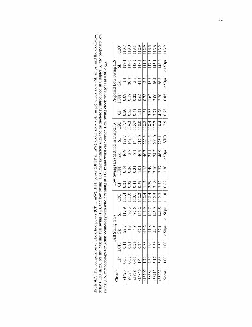
62
Tabl
e4.
7:T
heco
mpa
riso
nof
cloc
ktr
eepo
wer
(CP
inm
W),
DFF
pow
er(D
FFP
inm
W),
cloc
ksk
ew(S
k.in
ps),
cloc
ksl
ew(S
l.in
ps)
and
the
cloc
k-to
-qde
lay
(C2Q
inps
)fo
rth
eba
selin
efu
llsw
ing
(FS)
,the
low
swin
g(L
S)im
plem
enta
tion
with
the
met
hodo
logy
intr
oduc
edin
Cha
pter
3,an
dpr
opos
edlo
wsw
ing
(LS)
met
hodo
logy
for3
2nm
tech
nolo
gyw
ithw
ire
2ru
nnin
gat
1G
Hz
and
wor
stca
seco
rner
.Low
swin
gcl
ock
volta
geis
at0.
80×
V dd.
Cir
cuits
Full
Swin
g(F
S)L
owSw
ing
(LS)
Met
hod
inC
hapt
er3
Prop
osed
Low
Swin
g(L
S)C
PD
FFP
Sk.
Sl.
C2Q
CP
DFF
PSk
.Sl
.C
2QC
PD
FFP
Sk.
Sl.
C2Q
s142
30.
330.
1129
.711
2.9
111.
40.
210.
1446
.917
9.7
117.
70.
200.
091.
412
8.1
113.
7s9
234
0.52
0.21
1.3
90.5
111.
00.
320.
263.
714
9.4
116.
20.
350.
1820
.313
9.5
113.
0s5
378
0.65
0.25
4.8
87.6
110.
10.
410.
318.
114
4.4
115.
70.
410.
225.
614
3.2
113.
1s1
5850
1.60
0.76
47.1
136.
211
2.2
0.99
1.01
40.9
217.
011
8.0
1.21
0.65
41.3
148.
711
2.9
s132
071.
790.
8843
.214
1.9
112.
41.
121.
1546
.722
5.3
118.
21.
310.
7512
.514
1.7
112.
9s3
8584
4.52
1.90
41.8
145.
711
2.4
2.79
2.49
21.1
229.
511
8.4
3.35
1.62
45.7
147.
311
3.5
s384
175.
122.
3844
.514
5.9
112.
53.
183.
1024
.220
9.0
117.
73.
712.
0036
.414
5.1
113.
6s3
5932
5.66
2.59
32.1
141.
511
2.3
3.52
3.37
46.9
225.
111
8.4
4.28
2.20
26.8
148.
011
3.2
Nor
m.
1.00
1.00
<50
ps<
150p
s11
1.8
0.62
1.30
<50
psV
IO11
7.5
0.73
0.85
<50
ps<
150p
s11
3.2

63
Tabl
e4.
8:T
heco
mpa
riso
nof
cloc
ktr
eepo
wer
(CP
inm
W),
DFF
pow
er(D
FFP
inm
W),
cloc
ksk
ew(S
k.in
ps),
cloc
ksl
ew(S
l.in
ps)
and
the
cloc
k-to
-qde
lay
(C2Q
inps
)fo
rth
eba
selin
efu
llsw
ing
(FS)
,the
low
swin
g(L
S)im
plem
enta
tion
with
the
met
hodo
logy
intr
oduc
edin
Cha
pter
3,an
dpr
opos
edlo
wsw
ing
(LS)
met
hodo
logy
for3
2nm
tech
nolo
gyw
ithw
ire
1ru
nnin
gat
1.5
GH
zan
dw
orst
case
corn
er.L
owsw
ing
cloc
kvo
ltage
isat
0.90×
V dd.
Cir
cuits
Full
Swin
g(F
S)L
owSw
ing
(LS)
Met
hod
inC
hapt
er3
Prop
osed
Low
Swin
g(L
S)C
PD
FFP
Sk.
Sl.
C2Q
CP
DFF
PSk
.Sl
.C
2QC
PD
FFP
Sk.
Sl.
C2Q
s142
30.
210.
150.
276
.611
0.3
0.17
0.16
0.2
97.8
112.
70.
290.
1419
.682
.110
6.1
s923
40.
470.
3010
.879
.710
9.7
0.38
0.32
13.1
100.
111
2.0
0.43
0.27
5.2
75.7
106.
0s5
378
0.54
0.37
1.0
82.1
110.
70.
440.
391.
410
3.2
112.
90.
550.
331.
673
.410
6.5
s158
501.
441.
048.
687
.311
0.1
1.16
1.10
9.8
109.
111
2.5
1.46
0.97
33.7
86.6
106.
2s1
3207
1.71
1.22
4.5
85.9
110.
11.
371.
296.
210
8.3
112.
31.
591.
1212
.485
.510
6.0
s385
844.
172.
6128
.085
.510
9.7
3.35
2.76
35.9
107.
211
2.2
3.76
2.40
14.1
87.7
106.
1s3
8417
4.66
3.26
13.5
87.4
109.
93.
743.
4517
.211
0.0
112.
34.
492.
9736
.486
.810
6.1
s359
325.
043.
5811
.184
.810
9.9
4.05
3.80
15.7
107.
311
2.6
4.74
3.25
28.9
89.2
106.
0N
orm
.1.
001.
00<
50ps
<10
0ps
110.
10.
801.
06<
50ps
VIO
112.
40.
950.
91<
50ps
<10
0ps
106.
1

64
Tabl
e4.
9:T
heco
mpa
riso
nof
cloc
ktr
eepo
wer
(CP
inm
W),
DFF
pow
er(D
FFP
inm
W),
cloc
ksk
ew(S
k.in
ps),
cloc
ksl
ew(S
l.in
ps)
and
the
cloc
k-to
-qde
lay
(C2Q
inps
)fo
rth
eba
selin
efu
llsw
ing
(FS)
,the
low
swin
g(L
S)im
plem
enta
tion
with
the
met
hodo
logy
intr
oduc
edin
Cha
pter
3,an
dpr
opos
edlo
wsw
ing
(LS)
met
hodo
logy
for3
2nm
tech
nolo
gyw
ithw
ire
2ru
nnin
gat
1.5
GH
zan
dw
orst
case
corn
er.L
owsw
ing
cloc
kvo
ltage
isat
0.95×
V dd.
Cir
cuits
Full
Swin
g(F
S)L
owSw
ing
(LS)
Met
hod
inC
hapt
er3
Prop
osed
Low
Swin
g(L
S)C
PD
FFP
Sk.
Sl.
C2Q
CP
DFF
PSk
.Sl
.C
2QC
PD
FFP
Sk.
Sl.
C2Q
s142
30.
480.
151.
679
.311
0.0
0.43
0.16
1.7
86.6
110.
70.
430.
151.
786
.710
8.8
s923
40.
770.
311.
390
.911
1.1
0.69
0.31
1.0
99.2
111.
80.
750.
299.
790
.310
8.6
s537
80.
970.
374.
987
.611
0.0
0.87
0.38
5.2
95.7
111.
10.
940.
355.
688
.410
8.9
s158
502.
891.
079.
390
.510
9.9
2.59
1.09
11.2
99.2
110.
52.
721.
028.
694
.310
8.8
s132
073.
121.
2313
.687
.610
9.7
2.80
1.26
13.9
96.2
110.
92.
861.
1813
.392
.610
8.4
s385
847.
932.
6218
.894
.011
0.0
7.11
2.69
21.4
103.
011
1.0
7.66
2.52
33.9
92.0
108.
7s3
8417
8.74
3.26
10.1
92.8
110.
47.
853.
3411
.810
2.4
110.
98.
563.
1132
.887
.710
8.7
s359
3210
.13
3.56
17.5
90.7
109.
89.
083.
6418
.199
.711
0.9
9.60
3.41
29.2
93.1
109.
0N
orm
.1.
001.
00<
50ps
<10
0ps
110.
10.
901.
02<
50ps
VIO
111.
00.
960.
96<
50ps
<10
0ps
108.
7

65
Chapter 5: FINFET-BASED LOW SWING CLOCKING
A low swing clocking methodology is introduced to achieve low power operation at 20nm FinFET technol-
ogy. Low swing clock trees are used in existing methodologies, in order to decrease the dynamic power
consumption, in a trade-off for 3 issues: 1) The effect of leakage power consumption, which is becoming
more dominant when the process scales sub-32nm, 2) the increase in insertion delay, resulting in a high clock
skew, and 3) the difficulty in driving the existing DFF sinks with a low swing clock signal without a tim-
ing violation. In this chapter, a FinFET-based low swing clocking methodology is introduced to preserve
the dynamic power savings of low swing clocking while minimizing these three negative effects facilitated
through an efficient use of FinFET technology. At scaled performance constraints, the proposed methodol-
ogy at a 20nm FinFET technology leads to 42% total power savings (clock network+DFF) compared to a
FinFET-based full swing counterpart at the same frequency (3 GHz) thanks to the dynamic power savings of
low swing clocking. Furthermore, the proposed methodology achieves 3% power savings while doubling the
frequency, compared to a planar CMOS-based low swing implementation running at 1.5 GHz, thanks to the
leakage power savings of FinFET technology.
5.1 Introduction
FinFET-based circuits can be used to replace the incumbent planar CMOS-based circuits with existing meth-
ods, leading to improvements in static (i.e. leakage) power consumption. Alternatively, in a more methodical
manner, FinFET-based low power design methodologies can be developed. Unlike a straight-forward re-
placement, FinFET-aware methodologies would combine the leakage power superiority of the FinFETs with
1) dynamic power minimization techniques and 2) FinFET-specific design features, such as an increased fre-
quency operation, and the use of improved driving capability and low gate delay of FinFET devices. This
chapter describes one such advancement in the science of clock tree synthesis, facilitating the use of FinFET
technology.

66
The proposed design methodology achieves advancements in: i) low swing clock tree synthesis, and ii) a
novel DFF topology to accommodate low swing clocking. The outcome is a design methodology for low
swing clock tree synthesis in 20nm FinFET technology that demonstrates i) substantial dynamic power sav-
ings, leading to 36% in the clock tree power (excluding DFF) and 42% in total power (clock network+DFF)
compared to its full swing counterpart in FinFET technology operating at 3 GHz, compounded with ii) sub-
stantial leakage power savings, leading to a total power savings of 3% while doubling (from 1.5 GHz to
3 GHz) the frequency, compared to its planar CMOS counterpart running with a low swing clock. If the
improvements through the combination of low swing clocking and use of FinFETs are compared against a
traditional, full swing implementation with the planar CMOS technology, 24% power savings is obtained
in total power compared to a planar CMOS-based full swing implementation, while doubling the clock
frequency.
The proposed low swing clock tree design methodology is not a straight-forward procedure due to the
following issues:
1. Currently, there are no standard buffer or flip-flop libraries in FinFET technology that are available for
academic use, therefore, custom clock buffer and flip-flop designs are necessary.
2. The timing characterization of these custom FinFET-based buffer and flip-flop designs needs to be
performed at full swing and the target low swing voltage nodes so as to be used by the clock network
design methodology.
3. The differences in the input capacitance and the timing characteristics of the FinFET buffers compared
to planar CMOS buffers, and their relationship to interconnect scaling at sub-32nm technology, prohibit
a straight-forward planar CMOS-replacement approach, therefore, a methodical approach is necessary.
4. A novel, low swing flip-flop aware clock tree design methodology is necessary to provide clock trees
with the slew specifications of the original full swing clock tree.
The proposed methodology is implemented with i) a custom FinFET-based clock buffer with a selected driv-
ing capability considering the original design constraints of the full swing system, ii) a custom low swing
flip-flop design (low swing DFF) that has almost identical clock-to-q delay compared to traditional full swing

67
flip-flops. Timing characterization of the clock buffer and low swing DFF are performed so as to be used by
the clock tree design methodology. The clock tree design methodology consists of a clustering stage and a
novel buffering scheme to achieve low skew values while minimizing the power consumption of the clock
buffers and interconnects.
The rest of the chapter is structured as follows. In Chapter 5.2, the proposed methodology is introduced
and explained in detail. The experimental results are presented in Chapter 5.3 and the chapter is finalized
with concluding remarks in Chapter 5.4.
5.2 Methodology
The proposed design methodology that enables the implementation of low swing clock trees at a FinFET
technology node consists of 4 major steps:
1. design of a FinFET-based clock buffer library design, which is an optional step, required only if a
FinFET-based buffer library is not readily available.
2. timing characterization of the buffer library, which is another optional step, required only if the timing
models of the buffer library are not readily available.
3. design of a low swing DFF, which is a required step as the low swing DFF directly affects the overall
performance and the power consumption.
4. synthesis of a low swing DFF-aware clock tree, considering the timing constraints (clock skew and
slew) and the power consumption.
At the time of this dissertation, a FinFET-based standard cell library is not available for academic use.
Thus, a clock buffer is custom-designed, as explained in Chapter 5.2.1, so as to have similar driving capabil-
ities as the reference NBUFFX32 cell in the baseline planar CMOS-based buffer library (SAED32nm [59]
of Synopsys). This is important for a fair comparison between the implementations in the incumbent pla-
nar CMOS technology and the one proposed in the FinFET technology. The timing characterization of this
custom-designed buffer is presented in Chapter 5.2.2 so as to generate a timing model to be used at the clock
tree design step. After these optional steps, which are only performed due to the absence of a FinFET-based

68
cell library, the required steps of the proposed flow is similar to the automated flow for planar CMOS technol-
ogy shown in Figure 4.1. In the proposed flow, the low swing flip-flop, which is introduced in Chapter 5.2.3,
is designed considering the functionality, robustness, and power consumption. Then, the clock tree synthesis
is performed, which is presented in Chapter 5.2.4, considering the skew and the slew to target (almost) the
same performance on the local paths while saving significant power in the clock tree via low swing clocking.
5.2.1 FinFET-Based Clock Buffer Design
This step is optional, and is not necessary in the presence of a FinFET-based clock buffer library. The clock
buffer design presented here does not define the novelty of the presented work of this methodology, but
is needed to have a complete design flow. The design is limited to a single buffer, in order not to divert
the focus of the methodology to the (potentially sub-optimal) quality of the created buffer library. Instead,
having only one type of buffer highlights the elegance of the proposed FinFET-based low swing clocking
methodology. The custom clock buffer is designed to have a similar driving capability as the maximum size
buffer of the SAED 32nm library of Synopsys, namely NBUFFX32. As the transistor width and length are
process parameters in a FinFET technology, the sizing of the buffer is performed by changing the number of
fins. The number of fins is a discrete parameter whose optimal value cannot be computed through continuous
optimization methods. Instead, the desired number of fins is found with an iterative search. First, the second
inverter in the buffer is sized to achieve similar (close but not exact due to the discrete number of fins) driving
characteristics as NBUFFX32 when the input slew is at 50ps. Representative of a typical clock branch length
at the technology node, a 200µm wire is connected as the output load. In this scenario, the number of fins
is computed to be 29 for PFET and 25 for NFET. After this optimization, the number of fins of the first
inverter is changed so as to drive the second inverter with a similar slew value. The number of fins for the
NFET and the PFET of the first inverter of the buffer is determined to be 2. With this optimization, the
designed FinFET-based buffer and NBUFFX32 of SAED 32nm library drive the 200µm wire load with a
similar output slew (approximately 39ps and 37ps, respectively). The complete comparison of these two
buffers is summarized in Table 5.1. Having similar driving characteristics for both the FinFET and planar
CMOS buffers enables a fair comparison of technologies when two clock trees synthesized using these two
buffers are compared.

69
Table 5.1: The comparison of the custom-designed FinFET-based buffer and the planar CMOS-basedNBUFFX32 of SAED 32nm library.
Technology 1st Inverter (P/N) 2nd Inverter (P/N) Output Load Output Slew (ps)20nm FinFET 2fin/2fin 29fin/25fin 200µm wire 38.732nm Planar CMOS 800nm/420nm 800nm/420nm 200µm wire 37.2
5.2.2 Timing Characterization of the FinFET-Based Clock Buffer Design
The timing characterization of clock buffers can be performed in various ways. One option is to use higher
order models [40, 25] that can accurately estimate the timing characteristic of buffers at the expense of run
time. Another option is to store empirical data in lookup tables in order to decrease run time with similar
accuracy. For the proposed clock tree design methodology, a simple first order model is used as a third
option, as first order models are sufficient for the clock tree synthesis. The first order model helps achieve
substantial accuracy with simple metrics, which are also easily integrated into the clock tree design and
optimization process. A commonly used model for the clock buffers is the RC model, where each buffer
is modeled as a resistance (Rout ) and a capacitance (Cout ). With this model, it is easier to combine buffer
delay with the wire delay, which is also modeled as an equivalent RC network. Despite its simplicity, these
models produce substantially accurate timing metrics (such as Elmore delay [12]). With this observation,
the FinFET-based custom clock buffer introduced in Chapter 5.2.1 is characterized by sweeping the output
capacitance to estimate Rout and Cout . As the wire capacitance is dominant for sub-32nm technologies, the
wire length at the output is swept with desired data points, and the Rout and Cout can be obtained with a
linear fit on empirical data. For instance, the output load is swept from a 20µm wire to 200µm with 10 data
points for the experimental setup of this work. The accuracy of the adopted timing characterization metrics
is empirically demonstrated in the experimental results.
5.2.3 Low Swing DFF Design
The proposed DFF design is based on the low swing DFF topology introduced in Chapter 4.2.1. This topology
is implemented in FinFET technology, and the sizing of the transistors are performed to achieve similar clock-
to-q delay as its full swing counterpart. The conventional full swing latch in FinFET technology is shown in
Figure 5.1(a), and the proposed low swing latch used to build the low swing DFF is shown in Figure 5.1(b).

70
D
Q
CLK
CLK
CLK
T GN1
T GP1
T GP2
T GN2
(a) Classical full swing latch.
CLK
CLK
CLKD
Q
N1
N2
P2
X
P1
(b) Proposed low swing latch.
Figure 5.1: Latch schematics with FinFETs.
In order to compare the performance (i.e. clock-to-q delay) and the power consumption of two topologies,
both traditional full swing flip-flop (using two of the latches shown in Figure 5.1(a) in a master-slave latch
configuration) and the proposed low swing flip-flop (using two of the latches shown in Figure 5.1(b) in a
master-slave latch configuration) are implemented in 20nm FinFET technology, assuming a low swing voltage
at 0.7×Vdd . As clock-to-q delay depends on the slew at the clock pin, the clock slew is set to 50ps at full
Vdd and adjusted to 25ps for the 0.7×Vdd operation to achieve similar clock-to-q delay. The clock-to-q (C2Q)
delay and the power consumption of the conventional DFF topology when the clock input is at full Vdd , the
conventional DFF topology when the clock input is at 0.7×Vdd , and the proposed DFF topology when the
clock input is at 0.7×Vdd are compared in Table 5.2. It is important to note here that the supply voltages of data
paths are set as full Vdd at all three cases. It is shown in Table 5.2 that the clock-to-q delay of the conventional
DFF increases by ≈10ps when a low swing clock at 0.7×Vdd is applied. On the other hand, this increase
is 7.4ps and 7.8ps for the D = 1 and D = 0 cases, respectively, for the proposed DFF topology, limiting the
increase in clock-to-q delay by 2.2% and 2.3% of the clock period at 3 GHz, compared to the traditional full
swing flip-flop. Furthermore, it is important to note that there is contention current through the PFETs not

71
Table 5.2: The clock-to-q delay (C2Q) and the power consumption comparison of the conventional DFFtopology and the proposed low swing DFF topology in 20nm FinFET technology.
Power (µW) C2Q (D=1)(ps) C2Q (D=0)(ps)Conventional DFF: Data @Vdd , CLK @Vdd 5.4 21.4 20.4Conventional DFF: Data @Vdd , CLK @0.7×Vdd 7.6 31.9 31.3Proposed DFF: Data @Vdd , CLK @0.7×Vdd 2.7 28.8 28.2
completely turned off in the conventional DFF with clock at 0.7×Vdd case, similar to the contention current
through PMOS transistors in planar CMOS technology shown in Chapter 4.2.1. Thus, there is unstable
behavior resulting in possible failures due to the large current spikes generated by the contention current. It
is also shown that the power consumption of the conventional DFF increases significantly (from 5.4uW to
7.6uW) when a low swing clock is applied, as in the case of 32nm planar CMOS (shown in Figure 2.4). On
the other hand, the power consumption of the proposed DFF topology decreases significantly (from 5.4uW to
2.7uW). Thus, the proposed low swing DFF in FinFET technology has a superior behavior over a conventional
DFF, similar to the behavior for its planar CMOS counterpart (presented in Chapter 4).
5.2.4 Low Swing Clock Tree Design
In this subsection, the proposed low swing clock tree design methodology is introduced. The inputs of the
proposed algorithm are i) a placed design, with input capacitance information of flip-flop sinks, ii) the timing
models of the clock buffers and the clock wires, and iii) the skew and the slew constraints. With these inputs,
the algorithm returns the buffer and the wire locations, and their connectivity as the output. The algorithm is
presented in Algorithm 4.
The algorithm starts by initializing each sink as a node, and setting a bottom up delay (bottomup delay)
of 0 to each node (Lines 1-4), as these nodes are the leaves of the clock tree. Then, the algorithm searches
for the minimum cost (min cost) pair by iterating through all pairs (Lines 7-15). In the algorithm, the cost
is defined as the total capacitance: The sum of the capacitance of two nodes (i and j) to be merged, and
the capacitance of the interconnect that connects them (wirei, j). Once the minimum cost pair is found, these
nodes are recorded for merging (Lines 11-12). If a feasible pair is found (Line 16), the merging point of this
pair is calculated so as to have the same delay using the well-known deferred merge embedding for zero skew

72
Algorithm 4 FinFET-Based Low Swing Clock Tree Design MethodologyInput: DFF placement, timing models for the buffers and the interconnects, the skew and the maximum
capacitance constraint max cap.Output: Locations and connectivity information of clock buffers and interconnects.
1: Initialize each sink as a node2: for i in Nodes do3: bottomup delay(i)=04: end for5: while num of nodes > 1 do6: min cost=max cap7: for i in Nodes do8: for j in Nodes do9: if merging costi, j < min cost then
10: min cost=merging costi, j11: f oundi=i12: f ound j= j13: end if14: end for15: end for16: if min cost <= max cap then17: Find merging point( f oundi, f ound j,bottomup delay( f oundi),bottomup delay( f ound j))18: Create new node k, delete f oundi and f ound j19: bottomup delay(k) = (wire delay f oundi,k + bottomup delay( f oundi) + wire delay f ound j ,k +
bottomup delay( f ound j))/220:21: else22: Buffer all nodes23: Update their input capacitance24: end if25: end while
trees (ZST-DME) [5] routing algorithm (Line 17), these nodes are merged into a new node (k) (Line 18). If
wire snaking is necessary, it is avoided assuming a low power application, and the merging point is placed
on the child node where wire snaking is (e.g. would have been) necessary. The bottom up delay metric of
new node k is updated as the delay from the merging point to the its child (wire delayi,k) plus the bottom
up delay of that child (bottomup delay(i)). Note that the delay from this node to its two children is not
identical when the wire snaking is necessary (as the wire snaking is avoided). Thus, the bottom up delay
at this node is defined to be the average of the two bottom up delays calculated using bottom up delays of
two children (Line 19). If no feasible pair is found (Line 21), all nodes are buffered, although they do not
have the same capacitance (Lines 22-23). The purpose here is to create a balanced clock tree, i.e. reaching
each clock sink through the same number of levels. Having this uniform structure is very important for
73
low swing clock tree synthesis as the lack of uniformity can vary insertion delays significantly, resulting in
excessive clock skew. After buffering is performed, the capacitance values of these nodes are updated to be
the input capacitance of the buffer, and the same algorithm is followed recursively until only one node, i.e.
the clock source, is left (Lines 5-25). The algorithm successfully synthesizes a buffered bounded skew tree by
combining a well-known routing approach with a novel buffering scheme, addressing the lack of automation
tools in FinFET technology.
5.3 Experimental Analysis
The proposed methodology is implemented using a 20nm FinFET technology in comparison to a 32nm planar
CMOS technology. The experimental setup is introduced in Chapter 5.3.1 and the experimental results for
various cases are presented in Chapter 5.3.2 through Chapter 5.3.5. In particular, three primary goals of the
experiments are:
1. to evaluate the applicability of low swing clocking in a FinFET-based design as a dynamic power
saving (36% at the same frequency) methodology (Chapter 5.3.2).
2. to demonstrate that low swing clocking permits a higher frequency (2×) at the same power budget (3%
power savings) with a methodical implementation in FinFET technology, compared to its planar CMOS
counterpart (Chapter 5.3.3).
3. to demonstrate that low swing clocking provides significant power savings (46% power savings) at
the same frequency budget with a methodical implementation in FinFET technology, compared to its
planar CMOS counterpart (Chapter 5.3.4).
5.3.1 Simulation Setup
The proposed clock tree design methodology is coded in Perl, and tested on 3 largest circuits (s38584, s38417
and s35932) of ISCAS’89 benchmarks. It is noted here that ISPD’10 clock network contest benchmarks are
not usable for the proposed methodology in this study, as they lack the logic information for the local paths.
Instead, they have capacitance values, modeling clusters of flip-flop cells as a single capacitance. Thus, the
proposed low swing DFF cells, and the low swing DFF-aware clock tree design methodology cannot be tested

74
on those benchmarks. However, the maximum number of sinks in ISPD’10 benchmarks (2249) is comparable
to the maximum number of sinks in ISCAS’89 benchmarks (1728 for s35932), therefore, ISCAS’89 bench-
marks are sufficient to show the quality of results. The logic synthesis of the RTL netlists of the benchmark
circuits is performed using Design Compiler of Synopsys, and the placement of the flip-flop cells is per-
formed using IC Compiler of Synopsys in SAED 32nm planar CMOS technology [59] operating at 1.5 GHz.
As a complete cell library for 20nm FinFET technology is not available, the same DFF placement is used for
the experimental analysis performed in the FinFET technology node. This placement is not accurate, as the
FinFET-based cell library does not exist, but it serves to provide an attainable, re-producable approximation
to the expected placement in the absence of FinFET libraries. The FinFET-based clock buffer, introduced in
Chapter 5.2.3, and FinFET-based low swing DFF cell, introduced in Chapter 5.2.3, are implemented in the
PTM 20nm FinFET library [47]. The power and the skew analyses are performed using HSPICE simulator of
Synopsys. The full swing voltage levels are set as the default values in each technology, 1.05V and 0.9V for
the 32nm planar CMOS [59] and 20nm FinFET [47] technologies, respectively. The low swing voltage level
is assumed to be 70% of the nominal Vdd level at each case. The wire models for the 32nm technology are ob-
tained from [37], which has unit resistance and unit capacitance of R=8Ω/µm and C=0.2fF/µm, respectively,
with the default 50nm wire width. The wire models for 20nm technology are adopted from the 22nm technol-
ogy implementation in [3], which projects a 13% less capacitance from the 32nm technology implementation,
resulting in a C=0.174fF/µm. The per unit resistance remains the same as reported in [3], which is R=8Ω/µm.
The clock slew and the clock skew requirements of the FinFET-based and planar CMOS-based circuits are
selected to enable rational comparisons: As discussed in Chapter 5.2.3, the slew constraint is used as a proxy
for clock-to-q delay, where the clock-to-q delay is methodically mandated to remain the same regardless of
the presence of a low swing operation. To this end, for the FinFET-based circuits, the clock slew constraint
is set to 50ps for the full swing case, and 25ps for the low swing case. It is shown in Chapter 5.2.3 that the
clock-to-q delay at 70% of Vdd is≈28ps, almost the same as its full swing counterpart at a clock-to-q delay of
≈21ps with these slew constraints. For planar CMOS-based circuits at 1.5 GHz (half the frequency), the slew
constraint is set to 100ps, scaled proportionally from 50ps in the FinFET-based circuits. This constraint is
the same (100ps) for both low and full swing implementations because their clock-to-q delays are measured

75
Table 5.3: The comparison of clock buffer metrics (number of clock buffers/total buffer capacitance)and the clock interconnect metrics (total interconnect length/total interconnect capacitance) betweenthe FinFET-based low swing (LS) and FinFET-based full swing (FS) clock trees, reported with theinformation on benchmark circuits.
Circuit Floorplan Size Number of Clock Buffer Info (# / fF) Clock Interconnect Info (µm/fF)(µm×µm) Sinks FS LS FS LS
s38584 250×251 1239 86/12.9 220/33.0 14783/2572.2 14551/2531.9s38417 262×264 1461 94/14.1 247/37.1 16826/2927.7 16374/2849.1s35932 211×212 1728 88/13.2 259/38.9 16683/2902.8 16343/2843.7
to be identical with the same input slew, as shown in Chapter 4.3.3. The clock skew constraint is set to 50ps
for both technologies. This is considered reasonable, as the placements are identical for planar CMOS- and
FinFET-based circuits (due to the lack of a FinFET cell library).
5.3.2 Low Swing vs. Full Swing Clocking in FinFET Technology
The experimental results of the proposed FinFET-based low swing clocking methodology compared to its
full swing counterpart are presented in this subsection. The total clock buffer capacitance and the total clock
interconnect capacitance values are reported in Table 5.3, including the number of sinks and floorplan size
information of each benchmark circuit. The columns FS and LS demonstrate these clock network metrics for
the full swing and the low swing operation with FinFETs, respectively.
The increase in the number of clock buffers is expected for the low swing operation as the clock slew
constraint is set to 25ps (as opposed to 50ps in the full swing case) at that case to accommodate the low swing
DFF design. Partially compensating for the increase in the number of clock buffers, the total interconnect
length is smaller at the low swing case, thanks to the clustering algorithm working more efficiently with the
increased number of buffers in low swing clocking. It is observed in Table 5.3 that the increase in the total
capacitance is countered by the decrease in the interconnect capacitance, serving to minimize the overhead of
low swing clocking on the total switching capacitance. This observation is supported by the dynamic power
consumption comparison of the full swing and low swing implementations of the FinFET-based clock trees.
The comparison of the FinFET-based full swing clock tree against the FinFET-based low swing clock tree is
presented in Table 5.4. It is shown that there are significant power savings, which are recorded on average to
be 36% for the clock tree (excluding DFF power) and 52% for the DFF cells. Strikingly, these savings are

76
Table 5.4: The performance and power comparison of FinFET-based low swing (LS) and FinFET-basedfull swing (FS) clock trees at 3 GHz, reported separately for the clock network and the DFF cells.
Circuit CT Power (mW) DFF Power (mW) Skew (ps) Max Slew (ps) C2Q Delay (ps)FS LS FS LS FS LS FS LS FS LS
s38584 11.64 7.31 5.84 2.86 18.9 28.2 47.6 24.6 20.9 28.1s38417 13.02 8.25 6.97 3.33 21.1 41.7 47.9 24.9 21.0 28.7s35932 12.76 8.44 8.27 3.89 19.6 33.7 49.3 24.7 21.1 28.1Avrg. Imp. over FS 36% 52% -14.7 SATISFIED -7.3
recorded despite the number of clock buffers almost tripling to provide a sharper clock slew to the low swing
DFFs. It is iterated for a theoretical interpretation of the empirical result here that, the savings are at 36%,
less than the expected 51% savings from the ideal V 2dd savings (0.7×0.7=0.49). This degradation in power
savings is due to the fact that the input capacitance of low swing DFF cell is higher than the traditional full
swing DFF (0.23fF vs. 0.06fF). However, this degradation in the expected power savings is compensated by
the savings in the DFF power, thanks to the novel low swing DFF cell. It is shown in Table 5.4 that the power
savings at the DFF-only cells are 52%. The savings in the power consumption of the FinFET-based clock
networks through low swing clocking are realized via degrading the timing performance with a negligible
amount. It is shown in Table 5.4 that the degradation in the clock skew and the degradation in the clock-to-q
delay are 14.7ps and 7.3ps, respectively, totaling to a margin of 22.0ps within a clock cycle, which is still as
low as 6.6% of the clock period at a high speed 3 GHz operation.
For comparison purposes, the same algorithm (Algorithm 4) is used to design low swing and full swing
planar CMOS-based clock trees in SAED 32nm planar CMOS library [59]. The low swing DFF topology
is also implemented in this technology. The results are presented in Table 5.5. It is observed that power
savings can also be obtained in planar CMOS technologies via low swing clocking as was widely reported in
literature [2, 64] and in Chapter 4 of this dissertation. However, due to the superiority of the FinFET technol-
ogy (low leakage power, decreased performance overhead due to low buffer delay), the power savings of low
swing clock tree in FinFET technology are 6% more than its planar CMOS counterpart (36% vs. 30%). Fur-
thermore, the power savings at the DFF-only cells are as low as 3% in planar CMOS technology (compared
to 52% in FinFET technology). Note that the transistor delay (of the clock sub-circuit in DFF topology shown
in Figure 2.5) increases more significantly at a reduced voltage in planar CMOS technology than its FinFET
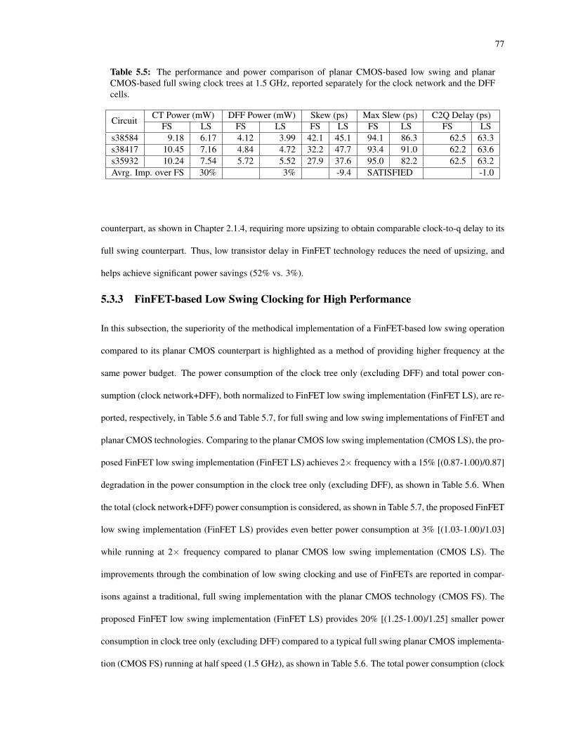
77
Table 5.5: The performance and power comparison of planar CMOS-based low swing and planarCMOS-based full swing clock trees at 1.5 GHz, reported separately for the clock network and the DFFcells.
Circuit CT Power (mW) DFF Power (mW) Skew (ps) Max Slew (ps) C2Q Delay (ps)FS LS FS LS FS LS FS LS FS LS
s38584 9.18 6.17 4.12 3.99 42.1 45.1 94.1 86.3 62.5 63.3s38417 10.45 7.16 4.84 4.72 32.2 47.7 93.4 91.0 62.2 63.6s35932 10.24 7.54 5.72 5.52 27.9 37.6 95.0 82.2 62.5 63.2Avrg. Imp. over FS 30% 3% -9.4 SATISFIED -1.0
counterpart, as shown in Chapter 2.1.4, requiring more upsizing to obtain comparable clock-to-q delay to its
full swing counterpart. Thus, low transistor delay in FinFET technology reduces the need of upsizing, and
helps achieve significant power savings (52% vs. 3%).
5.3.3 FinFET-based Low Swing Clocking for High Performance
In this subsection, the superiority of the methodical implementation of a FinFET-based low swing operation
compared to its planar CMOS counterpart is highlighted as a method of providing higher frequency at the
same power budget. The power consumption of the clock tree only (excluding DFF) and total power con-
sumption (clock network+DFF), both normalized to FinFET low swing implementation (FinFET LS), are re-
ported, respectively, in Table 5.6 and Table 5.7, for full swing and low swing implementations of FinFET and
planar CMOS technologies. Comparing to the planar CMOS low swing implementation (CMOS LS), the pro-
posed FinFET low swing implementation (FinFET LS) achieves 2× frequency with a 15% [(0.87-1.00)/0.87]
degradation in the power consumption in the clock tree only (excluding DFF), as shown in Table 5.6. When
the total (clock network+DFF) power consumption is considered, as shown in Table 5.7, the proposed FinFET
low swing implementation (FinFET LS) provides even better power consumption at 3% [(1.03-1.00)/1.03]
while running at 2× frequency compared to planar CMOS low swing implementation (CMOS LS). The
improvements through the combination of low swing clocking and use of FinFETs are reported in compar-
isons against a traditional, full swing implementation with the planar CMOS technology (CMOS FS). The
proposed FinFET low swing implementation (FinFET LS) provides 20% [(1.25-1.00)/1.25] smaller power
consumption in clock tree only (excluding DFF) compared to a typical full swing planar CMOS implementa-
tion (CMOS FS) running at half speed (1.5 GHz), as shown in Table 5.6. The total power consumption (clock

78
Table 5.6: The clock tree power (excluding DFF) comparison of the proposed FinFET-based lowswing (LS) clocking against the FinFET-based full swing (FS) clocking (both at 3 GHz), and planarCMOS-based low swing (LS) and full swing (FS) clocking (both at 1.5 GHz), normalized to FinFET-based low swing.
Circuit FinFET (@3 GHz) Planar CMOS (@1.5 GHz)FinFET LS FinFET FS CMOS LS CMOS FS
s38584 7.31 11.64 6.17 9.18s38417 8.25 13.02 7.16 10.45s35932 8.44 12.76 7.54 10.24Normalized Average Power 1.00 1.56 0.87 1.25
Table 5.7: The total (clock network+DFF) power comparison of the proposed FinFET-based lowswing (LS) clocking against the FinFET-based full swing (FS) clocking (both at 3 GHz), and planarCMOS-based low swing (LS) and full swing (FS) clocking (both at 1.5 GHz), normalized to FinFET-based low swing.
Circuit FinFET (@3 GHz) Planar CMOS (@1.5 GHz)FinFET LS FinFET FS CMOS LS CMOS FS
s38584 10.17 17.48 10.16 13.30s38417 11.58 19.99 11.98 15.29s35932 12.33 21.03 13.06 15.96Normalized Average Power 1.00 1.72 1.03 1.31
network+DFF) provides even better power savings at 24% [(1.31-1.00)/1.31] while doubling the frequency,
as shown in Table 5.7.
5.3.4 FinFET-based Low Swing Clocking for Ultra Low Power
With the use of FinFET technology, it is desired not only to reduce the leakage power but also to improve
performance through frequency scaling. However, FinFET technology can also be used in ultra low power
applications, taking advantage of low power structure of FinFETs at the same frequency constraints as planar
CMOS technology. In order to investigate this scenario for low power operation only, the power consump-
tion is also compared while both technologies are running at 1.5 GHz. The comparison of clock tree power
consumption only (excluding DFF) is presented in Table 5.8, and the comparison of the combined (clock
tree+DFF) power consumption is presented in Table 5.9. In this scenario for low power operation without
frequency scaling, the proposed FinFET low swing implementation (FinFET LS) can achieve 44% [(1.80-
1.00)/1.80] power savings at the clock tree only (excluding DFF) compared to planar CMOS low swing
implementation (CMOS LS), as shown in Table 5.8 at the same frequency constraint (1.5 GHz). When the
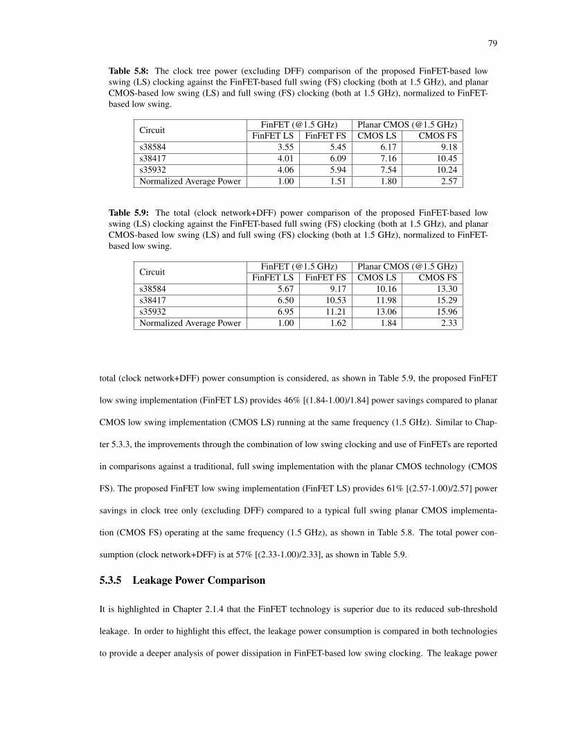
79
Table 5.8: The clock tree power (excluding DFF) comparison of the proposed FinFET-based lowswing (LS) clocking against the FinFET-based full swing (FS) clocking (both at 1.5 GHz), and planarCMOS-based low swing (LS) and full swing (FS) clocking (both at 1.5 GHz), normalized to FinFET-based low swing.
Circuit FinFET (@1.5 GHz) Planar CMOS (@1.5 GHz)FinFET LS FinFET FS CMOS LS CMOS FS
s38584 3.55 5.45 6.17 9.18s38417 4.01 6.09 7.16 10.45s35932 4.06 5.94 7.54 10.24Normalized Average Power 1.00 1.51 1.80 2.57
Table 5.9: The total (clock network+DFF) power comparison of the proposed FinFET-based lowswing (LS) clocking against the FinFET-based full swing (FS) clocking (both at 1.5 GHz), and planarCMOS-based low swing (LS) and full swing (FS) clocking (both at 1.5 GHz), normalized to FinFET-based low swing.
Circuit FinFET (@1.5 GHz) Planar CMOS (@1.5 GHz)FinFET LS FinFET FS CMOS LS CMOS FS
s38584 5.67 9.17 10.16 13.30s38417 6.50 10.53 11.98 15.29s35932 6.95 11.21 13.06 15.96Normalized Average Power 1.00 1.62 1.84 2.33
total (clock network+DFF) power consumption is considered, as shown in Table 5.9, the proposed FinFET
low swing implementation (FinFET LS) provides 46% [(1.84-1.00)/1.84] power savings compared to planar
CMOS low swing implementation (CMOS LS) running at the same frequency (1.5 GHz). Similar to Chap-
ter 5.3.3, the improvements through the combination of low swing clocking and use of FinFETs are reported
in comparisons against a traditional, full swing implementation with the planar CMOS technology (CMOS
FS). The proposed FinFET low swing implementation (FinFET LS) provides 61% [(2.57-1.00)/2.57] power
savings in clock tree only (excluding DFF) compared to a typical full swing planar CMOS implementa-
tion (CMOS FS) operating at the same frequency (1.5 GHz), as shown in Table 5.8. The total power con-
sumption (clock network+DFF) is at 57% [(2.33-1.00)/2.33], as shown in Table 5.9.
5.3.5 Leakage Power Comparison
It is highlighted in Chapter 2.1.4 that the FinFET technology is superior due to its reduced sub-threshold
leakage. In order to highlight this effect, the leakage power consumption is compared in both technologies
to provide a deeper analysis of power dissipation in FinFET-based low swing clocking. The leakage power
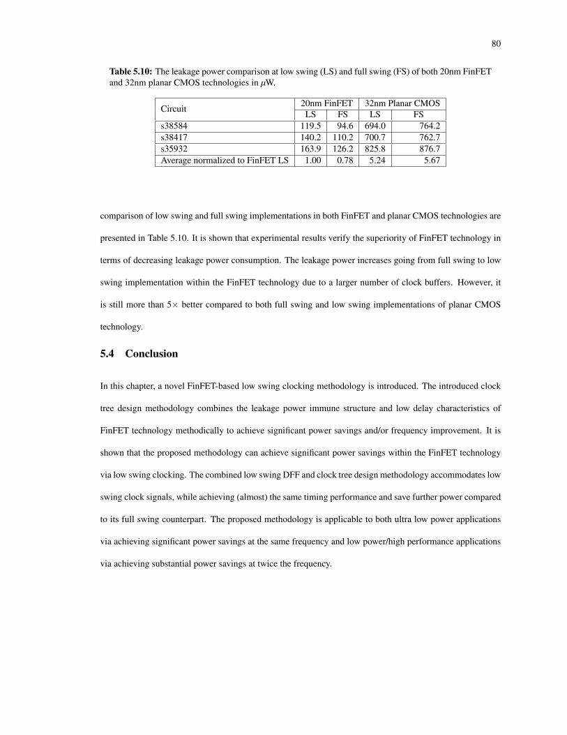
80
Table 5.10: The leakage power comparison at low swing (LS) and full swing (FS) of both 20nm FinFETand 32nm planar CMOS technologies in µW.
Circuit 20nm FinFET 32nm Planar CMOSLS FS LS FS
s38584 119.5 94.6 694.0 764.2s38417 140.2 110.2 700.7 762.7s35932 163.9 126.2 825.8 876.7Average normalized to FinFET LS 1.00 0.78 5.24 5.67
comparison of low swing and full swing implementations in both FinFET and planar CMOS technologies are
presented in Table 5.10. It is shown that experimental results verify the superiority of FinFET technology in
terms of decreasing leakage power consumption. The leakage power increases going from full swing to low
swing implementation within the FinFET technology due to a larger number of clock buffers. However, it
is still more than 5× better compared to both full swing and low swing implementations of planar CMOS
technology.
5.4 Conclusion
In this chapter, a novel FinFET-based low swing clocking methodology is introduced. The introduced clock
tree design methodology combines the leakage power immune structure and low delay characteristics of
FinFET technology methodically to achieve significant power savings and/or frequency improvement. It is
shown that the proposed methodology can achieve significant power savings within the FinFET technology
via low swing clocking. The combined low swing DFF and clock tree design methodology accommodates low
swing clock signals, while achieving (almost) the same timing performance and save further power compared
to its full swing counterpart. The proposed methodology is applicable to both ultra low power applications
via achieving significant power savings at the same frequency and low power/high performance applications
via achieving substantial power savings at twice the frequency.

81
Chapter 6: AN IMPROVED ALGORITHM FORSLEW-DRIVEN CLOCK TREE SYNTHESIS
A slew-driven clock tree synthesis (SLECTS) methodology is proposed to improve the quality of low voltage
clock trees. High interconnect resistance in the targeted state-of-the-art technologies dominates the device
resistance, especially in FinFET technologies, increasing the challenge of satisfying the slew constraint in
clock tree synthesis. This increase necessitates a paradigm shift from the traditional delay (and skew)-driven
methodology, such as the one in Chapter 4, to the proposed slew-driven methodology. SLECTS is developed
to i) satisfy tight slew constraints, which might be costly or infeasible with delay (skew)-driven methodolo-
gies and ii) reduce the power dissipation of the clock tree, thanks to targeting slew and skew constraints
simultaneously and methodically. The experimental results performed on ISPD’10 benchmarks on a 45nm
planar CMOS technology running at 1 GHz show that SLECTS achieves 7% and 17% savings compared to a
traditional skew-driven methodology at, respectively, the nominal Vdd voltage (0.9×Vdd at worst corner) and
a low voltage 0.7×Vdd operation (0.63×Vdd at worst corner). The improved savings in the power dissipation
at lower voltages are significant to demonstrate the value of SLECTS: The challenge in satisfying the slew
at low voltages is circumvented (through methodically controlling slew) with SLECTS, thereby providing
improved power savings (17% at 0.63×Vdd vs. 7% at 0.9×Vdd). Furthermore, the experimental analysis at
a 20nm FinFET technology has shown that up to 17% power savings are possible with SLECTS at 3 GHz
operation.
6.1 Introduction
The clock distribution network design is directly affected by the technology (i.e. interconnect and transistor)
scaling. In particular for clock slew, interconnect resistance significantly increases at every new technology
node [16]. The increase in the interconnect resistance makes it more challenging to satisfy slew constraints
on long wires. Furthermore, low voltage/swing IC design is becoming a norm to limit power density while
keeping up with Moore’s Law, which exacerbates clock slew. Despite the well-understood detrimental effects
of interconnect resistance and the low voltage on clock slew, using clock slew as a driving factor for clock tree

82
synthesis has not been investigated methodically. Instead, slew-constrained design techniques are proposed
in recent work [6, 31] and in the study performed in Chapter 4, to fix (or avoid) timing violations due to
slew. Exploiting slew-awareness as part of the clock tree synthesis (i.e. slew-driven) has not been previously
addressed.
The major contribution of this study is the introduction of a slew-driven CTS methodology called SLECTS.
SLECTS methodology is adept at delivering timing and power targets that are significantly more aggressive
compared to traditional delay/skew-driven CTS methodologies. Instead of targeting skew minimization as
the primary objective and resolving slew violations with buffer insertion with a capacitance or a slew bound,
as in traditional skew-driven CTS, SLECTS targets slew optimization at every stage of the synthesis, such
as clustering (i.e. merging) clock tree nodes, defining routing points and handling long interconnects. An-
other approach of traditional skew-driven CTS is to perform skew minimization in the first stage and resolve
slew violations in post-CTS optimization. SLECTS, on the other hand, uses buffering and clustering more
efficiently to constrain skew and slew simultaneously, so the tree is correct by design. Due to this efficient
slew handling and efficient use of buffering, SLECTS leads to reduced power dissipation while satisfying
the slew and skew constraints. In the algorithmic infrastructure developed on the popular deferred-merge-
embedding (DME) procedure, the proposed slew-driven CTS methodology features innovations of 1) a new
cost metric for the merging process, 2) a new merging point computation method, and 3) a new net splitting
method.
SLECTS is developed to replace the core DME routines that drive contemporary CTS tools. As a result,
contemporary skew-driven CTS tools will convert to a slew-driven flow, which is more appropriate for state-
of-the-art technologies. The experimental results demonstrate that the net splitting method is essential for
the slew-feasibility of a clock tree that has long interconnects. Cost metric and merging point computation
novelties complement the novelty of this methodology to improve the power consumption compared to ex-
isting methods. The final power savings compared to the (traditional, skew-driven) DME implementation of
Chapter 4 satisfying the same skew and slew constraints are 7% while operating at the nominal voltage (10%
off from Vdd at 0.9×Vdd at the worst corner) of a 1 GHz 45nm technology node. The power savings against
the conventional improve to 17% while operating at a lower voltage node (at 0.63×Vdd). The increased

83
savings of 17% (up from 7%) for 0.63×Vdd operation highlights the slew-driven approach of the proposed
methodology of this chapter in performing better in tighter slew constraints (i.e. at a lower voltage). As an
added analysis, experimentation with the FinFET-based technologies demonstrate that the proposed slew-
driven CTS methodology facilitates voltage and frequency scaling that is highly challenging in traditional
CTS methodologies. In this setup, the power savings are up to 10% at 2 GHz, and up to 17% in 3 GHz
compared to skew-driven CTS methodologies, validating the slew-driven approach of SLECTS at a 20nm
FinFET technology node [47]: Power savings of SLECTS improve at higher frequencies as the challenge of
handling slew increases.
The potential to i) perform voltage scaling and ii) achieve lower propagation delays with FinFET gates (that
permit frequency scaling) is well-known. In FinFET technology, the slew constraints are tighter due to these
multi-GHz frequencies of operation (i.e. through frequency scaling). One grand impact of SLECTS is to
satisfy these tighter slew constraints that are exacerbated by the increasing dominance of slew at lower volt-
ages (i.e. through voltage scaling). In brief, frequency scaling of CTS is enabled with SLECTS beyond those
that are economically possible with skew-driven CTS algorithms. This novelty not only enables clock signals
with higher operating frequencies to be distributed over a clock tree network, but also accomplishes this dis-
tribution with substantial power savings compared to skew-driven CTS methods. For reference, experimental
results in 20nm technology [47] show 55% and 51% power savings at 2 GHz and 3 GHz, respectively, when
the SLECTS power savings steps (merging pair selection and merging point computation) are combined with
the power savings through voltage scaling (that is enabled thanks to the net splitting method of SLECTS).
Furthermore, the efficient voltage scaling through SLECTS results in achieving 1.5× frequency (from 2 GHz
to 3 GHz) with an insignificant 3% increase in power consumption.
The rest of the chapter is organized as follows. The deferred merge embedding (DME) method is intro-
duced in Chapter 6.2. The proposed improvements to obtain the slew-driven clock tree synthesis (SLECTS)
methodology is presented in Chapter 6.3. The experimental results of the proposed methodology are pre-
sented in Chapter 6.4. The chapter is concluded in Chapter 6.5.
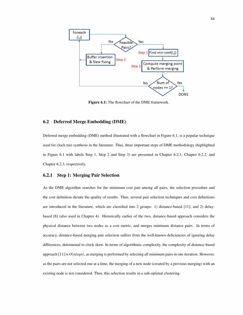
84
Step 1
Step 2
Step 3
Figure 6.1: The flowchart of the DME framework.
6.2 Deferred Merge Embedding (DME)
Deferred merge embedding (DME) method illustrated with a flowchart in Figure 6.1, is a popular technique
used for clock tree synthesis in the literature. Thus, three important steps of DME methodology (highlighted
in Figure 6.1 with labels Step 1, Step 2 and Step 3) are presented in Chapter 6.2.1, Chapter 6.2.2, and
Chapter 6.2.3, respectively.
6.2.1 Step 1: Merging Pair Selection
As the DME algorithm searches for the minimum cost pair among all pairs, the selection procedure and
the cost definition dictate the quality of results. Thus, several pair selection techniques and cost definitions
are introduced in the literature, which are classified into 2 groups: 1) distance-based [11], and 2) delay-
based [8] (also used in Chapter 4). Historically earlier of the two, distance-based approach considers the
physical distance between two nodes as a cost metric, and merges minimum distance pairs. In terms of
accuracy, distance-based merging pair selection suffers from the well-known deficiencies of ignoring delay
differences, detrimental to clock skew. In terms of algorithmic complexity, the complexity of distance-based
approach [11] is O(nlogn), as merging is performed by selecting all minimum pairs in one iteration. However,
as the pairs are not selected one at a time, the merging of a new node (created by a previous merging) with an
existing node is not considered. Thus, this selection results in a sub-optimal clustering.

85
The more contemporary and common of the two approaches, delay-based approach, is expectedly higher
in accuracy in terms of satisfying skew, the primary objective of traditional skew-driven CTS algorithms.
Delay is typically estimated with Elmore delay [12], and common merging pair cost computations consider
potential wire-snaking between candidate nodes, as well. The delay-based approach in [8], for instance, first
identifies the candidate merging node with the maximum delay target (i.e. candidate node with the minimum
insertion delay from the node to the clock sinks in its downstream). The approach then finds a minimum
cost pair for this node where cost is defined as the (e.g. Elmore) delay to a candidate pair node, including
the distance added to perform potential wire snaking. This approach provides better skew results (compared
to [11]), however, restricting the selection of the minimum insertion delay node as one of the pair does not
guarantee the minimum distance selection, thereby degrading clock slew. In terms of algorithmic complexity,
the maximum delay target node and its minimum cost pair are identified with a linear search [both O(n)
complexity], resulting in a complexity of O(n2).
6.2.2 Step 2: Merging Point Computation
After selecting the minimum cost pair, as described in Chapter 6.2.1, the merging point is determined to
perform routing of this pair. A common practice [8] is to select a specific point for merging considering skew,
using the zero-skew-tree DME (ZST-DME) algorithm [5], as performed in Chapter 4. The zero skew merging
point is computed as follows [8]:
Li =0.5cunitL(i, j)2 +L(i, j)C j
Ci +C j +L(i, j)cunit+
t j− tirunit(Ci +C j +L(i, j)cunit)
(6.1)
where L(i, j) is the distance between two nodes (µm), runit and cunit are the per unit resistance (Ω/µm) and
capacitance ( f F/µm) of the interconnect, respectively, ti and t j are the insertion delay from i and j to their
sinks, respectively, Ci and C j are the capacitance at nodes i and j, respectively. Another approach in [9]
proposes a bounded-skew-tree DME (BST-DME) to define merging regions considering the skew constraint
in the bottom-up phase, and picks the minimum wirelength point at each region in the top-down phase. This
early approach is applicable only in “unbuffered” clock routing. In practice (and literature), buffered clock
tree routing has long been the norm [8], particularly when satisfying the slew constraint is paramount. An-

86
other practice is to use ZST-DME or BST-DME approaches as a first step, while allowing slew violations,
and consider buffering as an added optimization step to remove violations. In slew-driven buffering, com-
puting merging regions at each iteration of the bottom-up phase is computationally expensive due to the
highly complex slew estimation equation (introduced in Chapter 6.3.2), and allowing slew violations results
in algorithmic decisions based on inaccurate(ly high) slew on the nodes with violations.
6.2.3 Step 3: Net Splitting
The high interconnect resistance of the scaled semiconductor technologies require even shorter wires to be
split which would not be necessary in older technologies. To this end, traditional DME-based CTS algorithms,
such as the one in Chapter 4, consider buffer insertion at the merging points only, and do not consider splitting
the net (i.e. with buffering) after selecting merging pairs. This would result in slew violations on long distance
nets and would not permit the desired voltage and frequency scaling. Thus, the contemporary approach is
to synthesize clock tree with slew violations and fix these violations later in the physical design flow, as a
post-CTS optimization.
6.3 Proposed Improvements over DME
In order to be compatible with the existing CTS methodologies, the proposed methodology of SLECTS is
developed within the DME framework through novel improvements. The slew driven novelties in SLECTS
are highlighted on the traditional DME framework in Figure 6.1 with labels Step 1, Step 2 and Step 3. In
particular, SLECTS consists of 3 novel contributions, which are:
1. a pair selection and cost metric definition considering physical distance for efficient sink cluster-
ing (Step 1),
2. a slew- and skew-aware merging point computation for routing (Step 2),
3. a slew- and insertion delay-aware net splitting (Step 3) to avoid slew violations.
6.3.1 Step 1: Improvements in Merging Pair Selection
The contemporary and common delay-based cost definitions in the merging pair selection has two drawbacks
making them formidable for SLECTS: 1) Delay-based cost results in pairing nodes that are physically farther

87
to minimize skew, which is detrimental to slew, 2) Considering wire snaking as part of cost metric is inaccu-
rate. Wire snaking is detrimental to slew, therefore, buffer insertion is a more viable option for the merging
pairs that requires significantly high wire snaking.
Consequently, in this study, the distance-based approach (similar to [11]) is selected as the cost metric
favoring reduced slew degradation on the path. It is important to note here that using a distance-based cost
results in several subtree clusters that have different capacitance and delay values. This would make merging
harder at the top-level of a clock tree due to the insertion delay mismatches. However, the potential effects of
these mismatches are fixed by buffer insertion and/or wire snaking, and the power overhead of these processes
are shown, experimentally, to be less than those necessary to fix slew following a traditional skew-driven
CTS application through DME. Overall, SLECTS uses the distance (i.e. wire length) between two nodes as
a cost metric for clustering nodes (i.e. merging), and utilizes slew with more accurate estimations (than net
length, such as the one introduced in Chapter 6.3.2). This is a striking conclusion and a drastic change from
traditional DME-based CTS routines.
Algorithmically, the merging pair selection in SLECTS is performed by considering all possible pairs (up
to n2 possibilities) at each iteration. This theoretical O(n3) complexity of this selection scheme is avoided
with data re-use. In the first iteration, the costs of all n2 pairs of initial n nodes are computed [complexity
of O(n2)]. Starting from the second iteration, only the costs of merging the recently added node with the
remaining (n− 1) nodes [O(n)] are computed [complexity of O(n2)] as the other pairing combinations are
already computed in the first iteration. Thus, although the asymptotic complexity is still O(n3), the algorithm
performs O(n2) computations and O(n3) look-ups. It is shown in the experimental results (Chapter 6.4) that
the run time of the proposed methodology has a quadratic dependence [O(n2)] on the circuit size.
6.3.2 Step 2: Improvements in Merging Point Computation
In this study, the skew constraint-based merging regions are constructed in the bottom-up phase, similar
to the BST-DME methodology [9]. Unlike BST-DME methodology where merging regions are propagated
in the bottom-up phase and the merging points are determined in the top-down phase, the merging point
is determined within this merging region considering the slew constraint in the same phase. This is an
algorithmic change from traditional BST-DME in order to satisfy skew and slew constraints simultaneously.
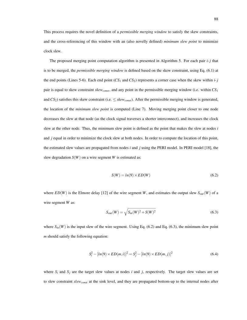
88
This process requires the novel definition of a permissible merging window to satisfy the skew constraints,
and the cross-referencing of this window with an (also novelly defined) minimum slew point to minimize
clock slew.
The proposed merging point computation algorithm is presented in Algorithm 5. For each pair i- j that
is to be merged, the permissible merging window is defined based on the skew constraint, using Eq. (6.1) at
the end points (Lines 5-6). Each end point (CS1 and CS2) represents a corner case when the skew within i- j
pair is equal to skew constraint skewconst , and any point in the permissible merging window (i.e. within CS1
and CS2) satisfies this skew constraint (i.e. ≤ skewconst ). After the permissible merging window is generated,
the location of the minimum slew point is computed (Line 7). Moving merging point closer to one node
decreases the slew at that node (as the clock signal traverses a shorter interconnect), and increases the clock
slew at the other node. Thus, the minimum slew point is defined as the point that makes the slew at nodes i
and j equal in order to minimize the clock slew at both nodes. In order to compute the location of this point,
the estimated slew values are propagated from nodes i and j using the PERI model. In PERI model [18], the
slew degradation S(W ) on a wire segment W is estimated as:
S(W ) = ln(9)×ED(W ) (6.2)
where ED(W ) is the Elmore delay [12] of the wire segment W , and estimates the output slew Sout(W ) of a
wire segment W as:
Sout(W ) =√
Sin(W )2 +S(W )2 (6.3)
where Sin(W ) is the input slew of the wire segment. Using Eq. (6.2) and Eq. (6.3), the minimum slew point
m should satisfy the following equation:
S2i − [ln(9)×ED(m, i)]2 = S2
j − [ln(9)×ED(m, j)]2 (6.4)
where Si and S j are the target slew values at nodes i and j, respectively. The target slew values are set
to slew constraint slewconst at the sink level, and they are propagated bottom-up to the internal nodes after
89
Algorithm 5 Merging Point ComputationInput: Insertion delays and locations of nodes i and j, skew constraint skewconst .Output: Location of new node k.
1: Maxi = max[Dins(i)]2: Max j = max[Dins( j)]3: Mini = min[Dins(i)]+ skewconst4: Min j = min[Dins(i)]+ skewconst5: Compute CS1 by computing LCS1 with Eq. (6.1) for ti = Maxi, t j = Min j6: Compute CS2 by computing LCS2 with Eq. (6.1) for ti = Mini, t j = Max j7: Compute min slew point m by solving Eq. (6.4)8: if min(CS1,CS2)< m < max(CS1,CS2) then9: Merging point k = m
10: else if min(CS1,CS2)> m then11: Merging point k = max(CS1,CS2)12: else13: Merging point k = min(CS1,CS2)14: end if
(a) Minimum slew point is within the permissible mergingwindow, it is set as the merging point.
(b) Minimum slew point is outside the permissible mergingwindow, the closest end point is set as the merging point.
Figure 6.2: Permissible merging window and min slew point definitions to identify the merging point.
each merging. After Eq. (6.4) is re-organized in a closed-form, it becomes a third-order equation (as Elmore
delay scales quadratically with wirelength). Thus, a single real positive root can be found when the equation
satisfies ∆<0. Note that, ∆>0 case only occurs when m is computed to be farther than j [i.e. L(m, i)> L( j, i)],
in which case m can directly be set to j. In other cases (i.e. when ∆ <0), the position of point m is checked
to identify whether it is within the permissible merging window (Line 8). If this is the case, m is set as the
merging point k, as shown in Figure 6.2(a) (Line 9). Otherwise, k is set as one of the corner points, as shown
in Figure 6.2(b), so as to satisfy skew constraints (Lines 10-13). For the cases where permissible merging
window does not exist (i.e. no possible point to satisfy skew constraint), buffer insertion (when the delay
mismatch is larger than one clock buffer delay) or wire snaking (when the delay mismatch is smaller than one
clock buffer delay) is considered.

90
(a) A naive location-based net splitting. (b) The proposed insertion delay-aware net splitting.
Figure 6.3: Slew-aware net splitting demonstration.
6.3.3 Step 3: Improvements in Net Splitting
SLECTS satisfies slew constraints while considering the insertion delays of the nodes to be merged. The
purpose of considering insertion delays is to avoid a high buffering and wire snaking cost that is induced by a
large mismatch between the insertion delays, and keep number of buffer levels balanced for PVT variations.
In order to highlight this phenomenon, a motivational example is presented in Figure 6.3. It is assumed that
three nodes i, j and k are to be merged and a single buffer insertion cannot satisfy the slew constraint at either
pair of nodes. Thus, the net of the selected pair of nodes needs to be split with buffer insertion to satisfy the
slew constraint. Assume that i- j pair has the lowest cost (i.e. minimum distance as defined in Chapter 6.3.1),
and is selected to be merged. A naive approach, depicted in Figure 6.3(a), could start splitting from node i
in order to bring the merging point closer to j and k for a lower merging cost in the next iteration. However,
this would significantly increase the insertion delay at node i, resulting in excessive buffering and/or wire
snaking when merging i with the other nodes. The insertion delay-aware net splitting technique, presented in
Algorithm 6, is proposed to address this issue. The proposed approach first finds the minimum cost pair (si
and s j in Line 4) and determines which node of the selected (i.e. minimum cost) pair has a smaller insertion
delay. Then, the distance is computed from this lower insertion delay node (either si in Line 8 or s j in Line 10)
to generate a new node m (Line 12). Starting net splitting from the node that has a smaller insertion delay
provides a more balanced buffering, such as the one depicted in Figure 6.3(b).

91
Algorithm 6 Net splitting for to avoid slew violationsInput: Insertion delays and locations of nodes i and j, slew constraint slewconst , timing information of clock
buffers and interconnects.Output: Location and insertion delay of new node m.
1: Costcurr = ∞
2: for (i, j) in Unmerged nodes do3: if Cost(i, j)<Costcurr then4: Costcurr =Cost(i, j),si = i,s j = j5: end if6: end for7: if Dins(si)< Dins(s j) then8: Compute L using Eq. (6.7) with si9: else
10: Compute L using Eq. (6.7) with s j11: end if12: Generate new node m at the computed location
In the proposed approach, the splitting point is determined as the longest feasible distance from the
selected (smaller insertion delay) node. The longest feasible distance is computed using the slew constraint,
the timing models of buffer and the interconnect metrics (per-unit resistance and capacitance). The output
slew S(B) of a buffer B is estimated as:
S(B) = Kslewcap ×Cout +Kslew (6.5)
in Chapter 4.2.2, where Kslewcap is the capacitance coefficient of output slew, Cout is the output capacitance
of the buffer B and Kslew is the no-load slew of the buffer. The slew propagation on the wire segment is
estimated using Eq. (6.2) and Eq. (6.3). Note that the input slew of the wire segment in Eq. (6.3) is equal to
the output slew of the buffer driving this wire [S(B) = Sin(W )]. Combining Eq. (6.5), Eq. (6.2) and Eq. (6.3),
the maximum distance L that a net can be split from a node i must satisfy the following equation:
Slewconst =√(Kslew
cap × (L× cunit +Capi))2 +(ln(9)×ED(W ))2 (6.6)
where cunit is the per-unit capacitance of the wire. As Elmore delay has quadratic dependence to distance L,
Eq. (6.6) is a fourth-order equation. However, the equation can be simplified by setting fixed values to discrete

92
variables, and assuming that they are constants. The discrete variables are the capacitance coefficient (Kslewcap )
of each buffer in the library, per-unit resistance (runit ) and capacitance (cunit ) of the clock routing layer. The
equation can be re-solved for each fixed case of these variables, making the capacitance at node i (Capi) the
only variable of the equation. After this simplification, the solution of L has a form of:
L =1
K1×Cap2i +K2×Capi +K3
(6.7)
where K1, K2 and K3 are the quadratic, linear and constant coefficients for the capacitive load at node i,
respectively. After the simplification, Eq. (6.7) can be solved for each clock buffer and clock routing layer
combination to generate coefficients (K1, K2 and K3) for each case. In this study, Matlab is used to obtain
these coefficients (K1, K2 and K3) by performing a quadratic fit for 1L . Once these coefficients are obtained
for each clock buffer and clock routing layer combination, they are placed into look-up tables. In this study,
the largest size buffer in the library is used in order to split as large distance as possible in one iteration.
6.4 Experimental Analysis
The simulation setup is described in Chapter 6.4.1. The experimental results for 45nm planar CMOS technol-
ogy [38] and 20nm FinFET technology [47] are presented in Chapter 6.4.2 and Chapter 6.4.3, respectively.
Run time analysis of the proposed methodology is performed in Chapter 6.4.4.
6.4.1 Simulation Setup
The proposed methodology is implemented with Perl and the quality of results is presented with select
ISPD’10 benchmarks. The power and the skew analyses are performed using HSPICE of Synopsys at 45nm
planar CMOS technology [38] and 20nm FinFET technology [47]. The benchmark circuits are operated at
1 GHz for 45nm planar CMOS technology, and at 2 GHz and 3 GHz for 20nm FinFET technology to study
frequency scaling. The wire models are obtained from ISPD’10 clock contest, which provides a per unit
resistance of R=0.3 Ω/µm and a per unit capacitance of C=0.16 fF/µm for 45nm technology. For the exper-
imental analysis of 20nm FinFET technology, the floorplan area, per unit resistance and capacitance of the
wire models and the sink capacitance values of ISPD’10 benchmarks are scaled by 0.25×, considering the

93
technology scaling (45nm to 20nm, square of technology scaling≈0.25). The slew constraint is set to 10% of
clock period for each frequency, and the skew constraint is set to 100ps and 50ps for 45nm planar CMOS and
20nm FinFET technologies, respectively. All experiments are performed at the worst PVT corner (0.9×Vdd ,
SS, 125C for 45nm planar CMOS, and 0.9×Vdd , SS, -40C for 20nm FinFET) to identify the lower bounds
of improvement of SLECTS.
In order to demonstrate the contribution of each step of the proposed methodology, four cases are gener-
ated as shown in Table 6.1. Two comparisons are performed with these four cases:
1. Case 1 vs. Case 2 to demonstrate the impact of the proposed pair selection scheme (Step 1).
2. Case 2 vs. Case 3 to demonstrate the impact of merging pair computation technique (Step 2).
Improvements due to Step 3 are a necessity in the proposed experimental flow (Case 0 vs. Case 1), as Case
0 implementation of the pair selection step 1 in [8] and merging point computation step 2 in [5] do not lead
to feasible clock trees (without net splitting technique introduced as step 3) for the ISPD’10 benchmarks (i.e.
slew/skew violations).
6.4.2 Results at 45nm Planar CMOS Technology
The results in Table 6.2 and Table 6.3 are presented for the nominal Vdd and low voltage (0.7×Vdd), respec-
tively. Note that the worst case Vdd is set as 0.90× each target Vdd , i.e. it is set to 63% of nominal Vdd when a
low voltage node that runs at 0.70×Vdd (0.70×0.90 = 0.63) is considered. These results highlight the power
savings provided by the proposed merging pair selection (Step 1) and merging point computation (Step 2)
methods with the presence of high interconnect resistance, enabled by the net splitting technique (Step 3) for
all cases. It is shown in Table 6.2 that the SLECTS methodology provides 7% power savings compared to
Table 6.1: Experimental setup for each step: Pair Selection (Step 1 in Figure 6.1), Merging PointComputation (Step 2 in Figure 6.1) and Net Splitting (Step 3 in Figure 6.1).
Step 1 Step 2 Step 3Case 0 Method in [8] Method in [5] N/ACase 1 Method in [8] Method in [5] Prop. methodCase 2 Prop. method Method in [5] Prop. methodCase 3 Prop. method Prop. method Prop. method

94
Table 6.2: Experiments 1 and 2 to demonstrate the impact of the proposed pair selection and mergingpoint computation schemes with reported clock slew (Sl.), clock skew (Sk.), and clock power (CP) atthe worst PVT corner of 1 GHz and 0.90×Vdd in 45nm planar CMOS technology.
Circuits Case 1 (DME) Case 2 Case 3 (SLECTS)Sl.(ps) Sk.(ps) CP(mW) Sl.(ps) Sk.(ps) CP(mW) Sl.(ps) Sk.(ps) CP(mW)
cns03 83.4 35.0 31.7 84.7 51.7 30 87.0 52.8 30.7cns04 86.4 79.5 41.5 86.5 55.4 37.4 89.8 41.8 37.2cns05 84.8 27.0 19.0 81.5 54.1 18.1 87.4 51.1 17.5cns06 84.5 42.4 24.9 82.3 32.8 25.1 88.2 63.5 24.1cns07 88.2 50.6 42.1 87.7 37.9 38.7 90.1 47.8 38.9cns08 85.0 44.0 29.7 83.2 32.4 26.8 92.9 48.2 26.6Norm. <100 <100 1.00 <100 <100 0.93 <100 <100 0.93
Table 6.3: Experiments 1 and 2 to demonstrate the impact of the proposed pair selection and mergingpoint computation schemes with reported clock slew (Sl.), clock skew (Sk.), and clock power (CP) atthe worst PVT corner of 1 GHz and 0.63×Vdd in 45nm planar CMOS technology.
Circuits Case 1 (DME) Case 2 Case 3 (SLECTS)Sl.(ps) Sk.(ps) CP(mW) Sl.(ps) Sk.(ps) CP(mW) Sl.(ps) Sk.(ps) CP(mW)
cns03 83.8 93.0 27.0 84.9 43.0 22.6 86.2 71.0 22.8cns04 85.6 83.0 31.4 85.4 51.0 26.8 85.5 92.0 27.4cns05 84.4 91.0 14.1 85.2 51.0 13.0 86.9 74.0 11.7cns06 85.6 81.0 18.8 87.3 96.2 18.4 90.8 84.6 18.4cns07 84.0 88.0 38.5 85.3 71.0 27.8 85.0 62.0 27.8cns08 84.3 69.0 24.3 85.3 47.5 20.3 85.2 77.9 19.8Norm. <100 <100 1.00 <100 <100 0.84 <100 <100 0.83
the traditional skew-driven DME-based CTS of Case 1 at 0.90×Vdd . Although the power savings are a mere
7% at 0.90×Vdd , the power savings of SLECTS methodology has an increasing trend with decreasing clock
voltage (tested at 10% decrements from Vdd , with 10% off for worst case operation): 7% at 0.90×Vdd (shown
in Table 6.2), 11% at 0.81×Vdd , 16% at 0.72×Vdd and 17% at 0.63×Vdd (shown in Table 6.3), compared to
Case 1 operating at the same Vdd fractions. This outcome verifies the slew-driven CTS claim of this study,
providing higher power savings when it is harder to satisfy slew constraints with reduced driving strength of
clock buffers (i.e. at lower voltage levels). It is concluded here that the proposed methodology can provide
significant power savings by enabling voltage scaling and exploiting slew. For reference, the power savings
of SLECTS at 0.63×Vdd is a substantial 33% compared to Case 1 (DME) running at 0.90×Vdd , when the
power savings of SLECTS and the power savings through voltage scaling enabled by SLECTS are combined.
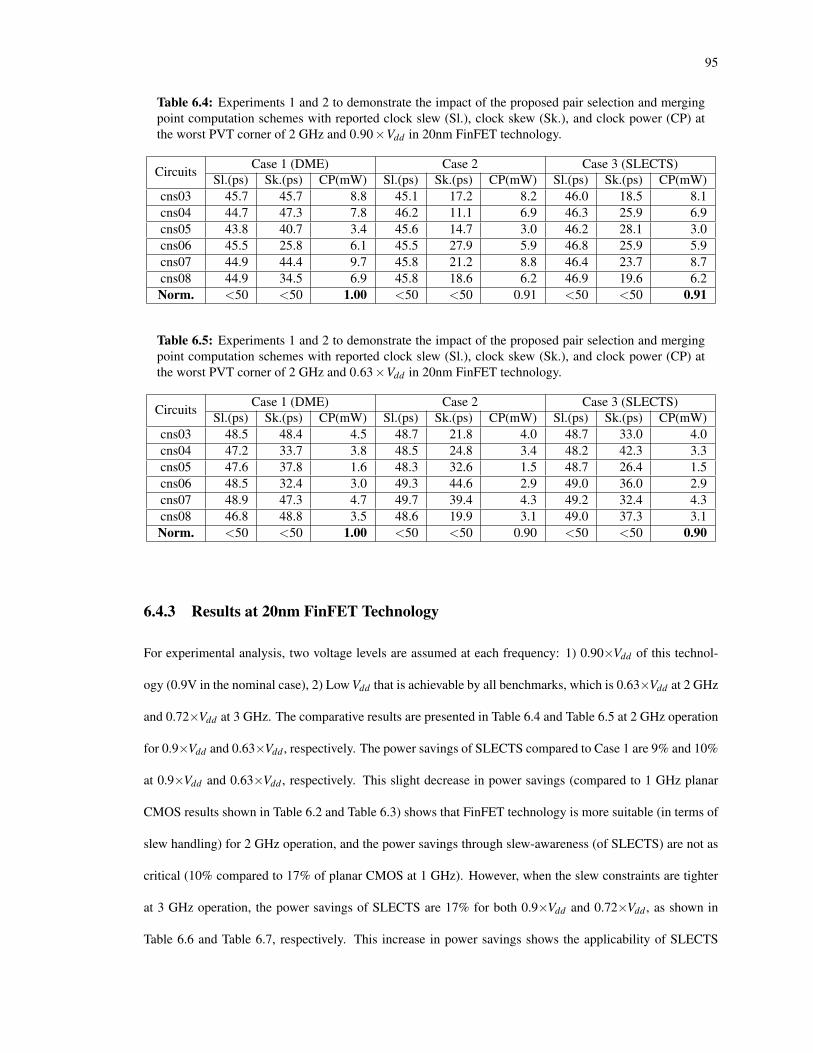
95
Table 6.4: Experiments 1 and 2 to demonstrate the impact of the proposed pair selection and mergingpoint computation schemes with reported clock slew (Sl.), clock skew (Sk.), and clock power (CP) atthe worst PVT corner of 2 GHz and 0.90×Vdd in 20nm FinFET technology.
Circuits Case 1 (DME) Case 2 Case 3 (SLECTS)Sl.(ps) Sk.(ps) CP(mW) Sl.(ps) Sk.(ps) CP(mW) Sl.(ps) Sk.(ps) CP(mW)
cns03 45.7 45.7 8.8 45.1 17.2 8.2 46.0 18.5 8.1cns04 44.7 47.3 7.8 46.2 11.1 6.9 46.3 25.9 6.9cns05 43.8 40.7 3.4 45.6 14.7 3.0 46.2 28.1 3.0cns06 45.5 25.8 6.1 45.5 27.9 5.9 46.8 25.9 5.9cns07 44.9 44.4 9.7 45.8 21.2 8.8 46.4 23.7 8.7cns08 44.9 34.5 6.9 45.8 18.6 6.2 46.9 19.6 6.2Norm. <50 <50 1.00 <50 <50 0.91 <50 <50 0.91
Table 6.5: Experiments 1 and 2 to demonstrate the impact of the proposed pair selection and mergingpoint computation schemes with reported clock slew (Sl.), clock skew (Sk.), and clock power (CP) atthe worst PVT corner of 2 GHz and 0.63×Vdd in 20nm FinFET technology.
Circuits Case 1 (DME) Case 2 Case 3 (SLECTS)Sl.(ps) Sk.(ps) CP(mW) Sl.(ps) Sk.(ps) CP(mW) Sl.(ps) Sk.(ps) CP(mW)
cns03 48.5 48.4 4.5 48.7 21.8 4.0 48.7 33.0 4.0cns04 47.2 33.7 3.8 48.5 24.8 3.4 48.2 42.3 3.3cns05 47.6 37.8 1.6 48.3 32.6 1.5 48.7 26.4 1.5cns06 48.5 32.4 3.0 49.3 44.6 2.9 49.0 36.0 2.9cns07 48.9 47.3 4.7 49.7 39.4 4.3 49.2 32.4 4.3cns08 46.8 48.8 3.5 48.6 19.9 3.1 49.0 37.3 3.1Norm. <50 <50 1.00 <50 <50 0.90 <50 <50 0.90
6.4.3 Results at 20nm FinFET Technology
For experimental analysis, two voltage levels are assumed at each frequency: 1) 0.90×Vdd of this technol-
ogy (0.9V in the nominal case), 2) Low Vdd that is achievable by all benchmarks, which is 0.63×Vdd at 2 GHz
and 0.72×Vdd at 3 GHz. The comparative results are presented in Table 6.4 and Table 6.5 at 2 GHz operation
for 0.9×Vdd and 0.63×Vdd , respectively. The power savings of SLECTS compared to Case 1 are 9% and 10%
at 0.9×Vdd and 0.63×Vdd , respectively. This slight decrease in power savings (compared to 1 GHz planar
CMOS results shown in Table 6.2 and Table 6.3) shows that FinFET technology is more suitable (in terms of
slew handling) for 2 GHz operation, and the power savings through slew-awareness (of SLECTS) are not as
critical (10% compared to 17% of planar CMOS at 1 GHz). However, when the slew constraints are tighter
at 3 GHz operation, the power savings of SLECTS are 17% for both 0.9×Vdd and 0.72×Vdd , as shown in
Table 6.6 and Table 6.7, respectively. This increase in power savings shows the applicability of SLECTS
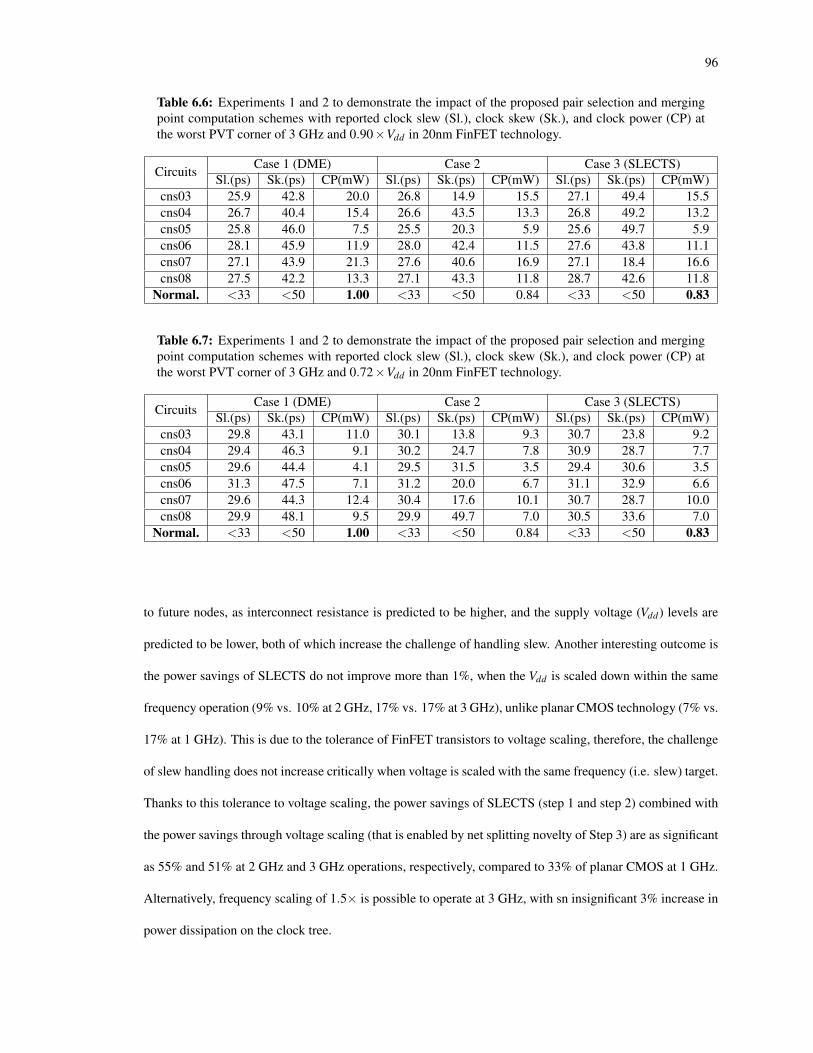
96
Table 6.6: Experiments 1 and 2 to demonstrate the impact of the proposed pair selection and mergingpoint computation schemes with reported clock slew (Sl.), clock skew (Sk.), and clock power (CP) atthe worst PVT corner of 3 GHz and 0.90×Vdd in 20nm FinFET technology.
Circuits Case 1 (DME) Case 2 Case 3 (SLECTS)Sl.(ps) Sk.(ps) CP(mW) Sl.(ps) Sk.(ps) CP(mW) Sl.(ps) Sk.(ps) CP(mW)
cns03 25.9 42.8 20.0 26.8 14.9 15.5 27.1 49.4 15.5cns04 26.7 40.4 15.4 26.6 43.5 13.3 26.8 49.2 13.2cns05 25.8 46.0 7.5 25.5 20.3 5.9 25.6 49.7 5.9cns06 28.1 45.9 11.9 28.0 42.4 11.5 27.6 43.8 11.1cns07 27.1 43.9 21.3 27.6 40.6 16.9 27.1 18.4 16.6cns08 27.5 42.2 13.3 27.1 43.3 11.8 28.7 42.6 11.8
Normal. <33 <50 1.00 <33 <50 0.84 <33 <50 0.83
Table 6.7: Experiments 1 and 2 to demonstrate the impact of the proposed pair selection and mergingpoint computation schemes with reported clock slew (Sl.), clock skew (Sk.), and clock power (CP) atthe worst PVT corner of 3 GHz and 0.72×Vdd in 20nm FinFET technology.
Circuits Case 1 (DME) Case 2 Case 3 (SLECTS)Sl.(ps) Sk.(ps) CP(mW) Sl.(ps) Sk.(ps) CP(mW) Sl.(ps) Sk.(ps) CP(mW)
cns03 29.8 43.1 11.0 30.1 13.8 9.3 30.7 23.8 9.2cns04 29.4 46.3 9.1 30.2 24.7 7.8 30.9 28.7 7.7cns05 29.6 44.4 4.1 29.5 31.5 3.5 29.4 30.6 3.5cns06 31.3 47.5 7.1 31.2 20.0 6.7 31.1 32.9 6.6cns07 29.6 44.3 12.4 30.4 17.6 10.1 30.7 28.7 10.0cns08 29.9 48.1 9.5 29.9 49.7 7.0 30.5 33.6 7.0
Normal. <33 <50 1.00 <33 <50 0.84 <33 <50 0.83
to future nodes, as interconnect resistance is predicted to be higher, and the supply voltage (Vdd) levels are
predicted to be lower, both of which increase the challenge of handling slew. Another interesting outcome is
the power savings of SLECTS do not improve more than 1%, when the Vdd is scaled down within the same
frequency operation (9% vs. 10% at 2 GHz, 17% vs. 17% at 3 GHz), unlike planar CMOS technology (7% vs.
17% at 1 GHz). This is due to the tolerance of FinFET transistors to voltage scaling, therefore, the challenge
of slew handling does not increase critically when voltage is scaled with the same frequency (i.e. slew) target.
Thanks to this tolerance to voltage scaling, the power savings of SLECTS (step 1 and step 2) combined with
the power savings through voltage scaling (that is enabled by net splitting novelty of Step 3) are as significant
as 55% and 51% at 2 GHz and 3 GHz operations, respectively, compared to 33% of planar CMOS at 1 GHz.
Alternatively, frequency scaling of 1.5× is possible to operate at 3 GHz, with sn insignificant 3% increase in
power dissipation on the clock tree.

97
Figure 6.4: The run time of SLECTS vs. number of clock sinks, compared to its quadratic fit.
6.4.4 Run Time Analysis
As explained in Chapter 6.3.1, the asymptotic O(n3) complexity of merging pair selection algorithm has
reduced to O(n2) with data re-use. In order to empirically verify this, the run time of SLECTS as a function of
number of clock sinks is plotted, and presented in Figure 6.4. It is shown that the run time has a O(n2) profile,
matching well to the quadratic fit, with R2=0.99. For comparison purposes, the run times of all cases (Case 1
through Case 3) are presented in Table 6.8. As the run time depends solely on the number of sinks, the run
time for only one representative case (45nm planar CMOS at 1 GHz and 0.63×Vdd) is reported. Although all
cases have the same complexity [O(n2)], the run time of Case 2 is significantly better than Case 1 (≈3.3×).
This speedup is due to the proposed data re-use introduced in Chapter 6.3.1 performing better than targeting
the node with minimum delay at each iteration, as proposed in [8]. The run time of Case 3 is slightly higher
than Case 2 due to the additional cost of computing minimum slew point in Step 2 (Chapter 6.3.2). For
SLECTS, the benchmark with the highest run time is cns07 (which has the highest number of clock sinks of
1915) with a run time of 976 seconds (≈16 minutes). Note that this run time is significantly smaller than the
run time limit (12 hours) of ISPD’10 clock contest (from where the benchmark circuits and the experimental
setup are adopted).

98
Table 6.8: Run time comparison of all cases in 45nm planar CMOS technology at 1 GHz and 0.63×Vdd ,in seconds.
Circuits Case 1 (DME) Case 2 Case 3 (SLECTS)cns03 791 239 274cns04 2756 806 851cns05 485 142 156cns06 427 139 149cns07 3148 909 976cns08 661 212 230
Normalized 1.00 0.30 0.32
6.5 Conclusion
In this chapter, a slew-driven clock tree synthesis (SLECTS) methodology is introduced. In SLECTS, the
high interconnect resistance is managed with a net splitting technique on long wires, and new merging point
selection and computation techniques are introduced for power savings. The proposed methodology is shown
to be effective for power savings, increasingly at lower voltage nodes. Thus, it is highly applicable for low
power designs. Furthermore, the SLECTS methodology has been verified on FinFET-based clock trees to
achieve voltage scaling for low power or frequency scaling for performance, while providing additional power
savings compared to existing methodologies. SLECTS can be integrated into contemporary academic and
industrial CTS tool flows for a slew-driven approach, similar to DME having been popular for the traditional
skew-driven CTS approaches.

99
Chapter 7: AN IMPROVED ALGORITHM FORLOW SWING GATED CLOCK TREE SYNTHESIS
In this chapter, a novel algorithm is proposed for low swing gated clock tree synthesis. In gated clock
tree synthesis, it is a challenging problem to satisfy the skew constraint across the gated and non-gated
sinks. This challenge is exacerbated when clock swing is reduced for a low power operation. The proposed
methodology of this chapter synthesizes a low swing gated clock tree to combine power savings of low swing
clocking and clock gating, while addressing these challenges to satisfy both clock skew and slew constraints.
The experimental results performed on the large circuits of ISCAS’89 benchmarks operating at 1.5 GHz
in the 45nm technology show that the proposed methodology satisfies tight skew (50ps) and slew (100ps)
constraints that a previous gated clock tree synthesis methodology is not able to satisfy. Even though the
previous gated clock tree synthesis methodology can be combined with a prescribed skew approach to satisfy
these constraints, the proposed methodology still outperforms in power savings by 20%.
7.1 Introduction
Clock gating is a popular technique for low power ICs [21, 30, 31, 45, 7, 15]. In this study, a novel low swing
gated clock tree synthesis methodology is introduced to combine the power savings of low swing clocking
and clock gating. The proposed methodology is adept at satisfying tight clock timing constraints. True to
typical physical design flow, the connectivity and placement of clock gates, determined at the synthesis and
placement stages, respectively, are preserved. The proposed methodology has a two-stage approach. In the
first stage, local clock trees are synthesized for each local clock gate cluster (i.e. clock sinks under the same
clock gate) and buffer insertion, if necessary, is performed to satisfy the slew constraint. In the second stage,
top-level clock tree is generated by utilizing a prescribed skew approach along with a novel delay insertion
scheme to deliver the clock signal to the clock gate inputs and non-gated clock sinks. The prescribed skew ap-
proach is instrumental in providing the flexibility to handle different local clock tree insertion delays (induced
by the varying fanout sizes of clock gates) and insertion delays of non-gated clock paths, and the delay inser-
tion scheme is instrumental to satisfy the skew constraint. Both of these proposed local and top-level clock

100
tree synthesis procedures utilize a slew-aware buffer insertion methodology in order to avoid slew violations
in low swing operation. The outcome of this two-stage clock tree synthesis proposal is a low swing gated
clock tree that satisfies tight skew and slew constraints thanks to the novelties of slew-awareness and integra-
tion of prescribed skew. The experimental results performed on seven circuits from ISCAS’89 benchmarks
operating at 1.5 GHz in 45nm technology [38] show that the proposed methodology:
1. satisfies tight clock skew (50ps) and slew (100ps) constraints, where the previous gated clock tree syn-
thesis methodology [45] cannot synthesize feasible clock trees due to the excessive wire snaking (per-
formed to satisfy the skew constraint) resulting in slew violations,
2. achieves 20% power savings compared to the combination of the gated clock tree synthesis methodol-
ogy [45] and a prescribed skew approach [8] that satisfies the same clock skew (50ps) and slew (100ps)
constraints.
The rest of the chapter is organized as follows. The background information on clock gating is presented
in Chapter 7.2. The proposed methodology is introduced and explained in detail in Chapter 7.3. The experi-
mental results are presented in Chapter 7.4. The chapter is finalized with concluding remarks in Chapter 7.5.
7.2 Background
Clock gating is a popular low-power methodology that has been well-studied in the literature [21, 30, 31, 45,
7, 15]. In [21], a methodology is proposed to optimize the location of clock gates in the clock tree, and in [30],
a clock gate cloning and register merging methodology is introduced for power minimization. A clock skew
scheduling approach is considered in our collaborative study [27] to improve available timing slack. These
methodologies consider post-CTS optimization on already existing clock trees (in essence, orthogonal to the
work in this study). In [31], a gated clock tree synthesis is considered while considering the activity patterns
for power optimization and assuming a symmetrical tree structure that achieves bounded clock skew. In [45],
a zero skew gated clock tree synthesis methodology is proposed where the clock skew is minimized with wire
snaking at necessary clock branches. In [7], a type-matching algorithm is proposed where the clock buffers
at the same clock tree level as clock gates are replaced with clock gates to obtain a uniform structure and
minimize clock skew. In [15], a delay-matching approach is proposed where clock gates and clock buffers

101
Figure 7.1: Motivational example: 4 sinks on the left are gated and 4 sinks on the right are non-gated.Thus, this results in 5 sinks with different initial delays at the top-level clock tree.
with identical driving strengths are re-sized to balance insertion delays of gated and non-gated paths in the
clock tree and minimize clock skew.
A common scenario in today’s designs is to clock gate some (typically high) portion of clock sinks,
and keep high activity clock sinks non-gated. In such a scenario, gated clock tree synthesis encounters an
additional challenge due to the insertion delay mismatch between the gated and the non-gated clock paths. In
order to highlight this mismatch, a motivational example is presented in Figure 7.1. In Figure 7.1, four sinks
on the left are gated with one common ICG cell and the other four on the right are non-gated. A two-level
local clock tree is built for the gated portion sourced at the top-level ICG cell. After local clock tree synthesis,
there are five sinks for the top-level clock tree with non-equal target delays: Four non-gated sinks on the right
that have no children, and one sink (clock pin of ICG cell) on the left that has the delay of the ICG cell plus
insertion delay of the local clock tree. The assumption of a symmetrical clock tree in [31] is not valid in this
scenario, and the non-uniformity of gated and non-gated sinks results in excessive clock skew. In [45], clock
skew is minimized through wire snaking, which is prohibitive when the delay mismatch between gated and
non-gated paths requires excessive wire snaking, resulting in slew violations. The type-matching approach
in [7] is prohibitive as clock gates can be at any level of the tree, requiring many (or all) clock buffers to be
swapped with clock gates. Finally, the delay-matching approach in [15] requires re-sizing of clock buffers
and ICG cells for each target technology and voltage level, which is impractical. It is important to note here
that the mismatch between gated and non-gated paths (shown in Figure 7.1) is more significant in low swing
operation, resulting in high insertion delay mismatches.

102
It is concluded here that a low swing gated clock tree synthesis methodology needs to address clock
skew challenges between gated and non-gated paths of the clock tree and clock slew challenges of low swing
operation concurrently. To this end, the proposed methodology presented in Chapter 7.3 exploits a prescribed
skew approach along with a novel delay insertion scheme to satisfy the skew constraint, and considers a
slew-aware buffer insertion scheme to satisfy the slew constraint.
7.3 Methodology
The low swing gated clock tree synthesis methodology has a two-stage bottom-up flow based on well-known
deferred-merge-embedding (DME) method with proposed improvements described in Chapter 7.3.1. The
first stage, described in Chapter 7.3.2, is local clock tree synthesis when connectivity and placement of ICG
cells determined at the logic and physical synthesis stages are preserved. The second stage, described in
Chapter 7.3.3, details the top-level clock tree synthesis that uses a prescribed skew approach along with a
novel delay insertion scheme to address clock skew challenge introduced by clock gating. Both stages utilize
a slew-aware buffer insertion methodology to address clock slew challenge at low swing operation. The time
complexities of the algorithms are presented in Chapter 7.3.4, demonstrating the scalability of the proposed
low swing gated CTS methodology.
7.3.1 DME Method with Proposed Improvements
DME is a well-known methodology for zero skew [5] and bounded skew [9] routing whose buffered ver-
sions are adapted for clock tree synthesis in literature [45, 11, 8], and the methodology in Chapter 4. The
DME method, outlined in Algorithm 7, provides a flexible framework adopted for zero skew [11], prescribed
skew [8], and gated [45] CTS by considering different set of candidate nodes for merging (line 1), and us-
ing different cost (line 6) and feasibility metrics (line 5). For instance, all pairs of nodes are considered as
candidates for merging in the methodologies of [45, 11] whereas in the methodology of [8], the node with
the minimum insertion delay is enforced to be in the pair to minimize insertion delay. Cost metric is defined
as the distance between two nodes in the methodologies of [45, 11], and in the methodology of [8] and the
methodology introduced in Chapter 4, it is defined as the distance added with the potential wire snaking
between two nodes to consider the delay differences. As for the feasibility metric, the methodologies in

103
Algorithm 7 Traditional DME Algorithm used for CTSInput: Location and capacitance information of clock sinks, cost and feasibility metrics.Output: Locations and connectivity information of clock buffers and interconnects.
1: Select a subset of candidate nodes2: Costcurr=∞
3: for i in Canditate Nodes do4: for j in Candidate Nodes do5: if Cost(i, j) < Costcurr && Feasible(i, j) == 1 then6: Costcurr=Cost(i, j)7: end if8: end for9: end for
10: if Costcurr != ∞ then11: Perform merging to initialize new node k=Ti, j12: else13: for i in Unmerged Nodes do14: Insert buffer to fix violations.15: end for16: end if
[45, 8, 11] use a maximum capacitance constraint, and the methodology introduced in Chapter 4 considers a
maximum slew constraint.
In this study, the traditional DME method is adopted with feasibility metric defined as the maximum slew
constraint (as in the methodology introduced in Chapter 4) and distance as the cost metric (as in [45, 11]).
The novelty of the proposed methodology is introduced in the selection of candidate nodes for merging,
and it is complemented by a novel delay insertion methodology to satisfy clock skew constraint. For gated
clock trees, selecting pairs that have similar delay characteristics is critical to avoid skew violations between
the nodes of the pair. However, selecting pairs that are physically apart requires long interconnect between
the nodes of the pair, potentially causing slew violations. In order to consider skew and slew concurrently,
a novelly defined candidate window is introduced in the proposed methodology. The candidate window
is the insertion delay window that spans the minimum insertion delay node and the nodes whose insertion
delays are within the minimum insertion delay plus skew constraint skewconst , as shown in Figure 7.2. As
the difference between any pair of insertion delays is smaller than the skew constraint, all combination of
pairs selected within the candidate window satisfies the skew constraint. After the candidate window is
constructed (line 1), the pair with the minimum cost (i.e. distance) is selected to minimize interconnection,

104
Figure 7.2: The candidate window is defined as the insertion delay window between the minimuminsertion delay of all nodes and its skewconst neighborhood.
Initialize sink delays as 0
Use DME for merging of all pairs
Connect local source to ICG
Slew violation at
ICG?
Buffer insertion to local source
Done
YesNo
Figure 7.3: The flowchart for the local clock tree synthesis.
thereby minimizing degradation in slew. If the minimum cost pair is feasible (i.e. no slew violation), merging
of this pair is performed (line 11), and the candidate window is updated to reflect the change in the timing
information (insertion delay and slew) of this node. If all pairs are infeasible, buffer insertion is performed at
all nodes to avoid a slew violation (line 14), and the same procedure is followed until all nodes are merged.
The specific use of Algorithm 7 for each stage is explained in Chapter 7.3.2 and Chapter 7.3.3.
7.3.2 Local Clock Tree Synthesis
The local clock trees for each clock gate cluster are synthesized using the flow in Figure 7.3, based on
Algorithm 7. Furthermore, an additional step is introduced in the form of buffer insertion to satisfy the slew
constraint. At the first step, the algorithm initializes each clock sink within the clock gate cluster with zero
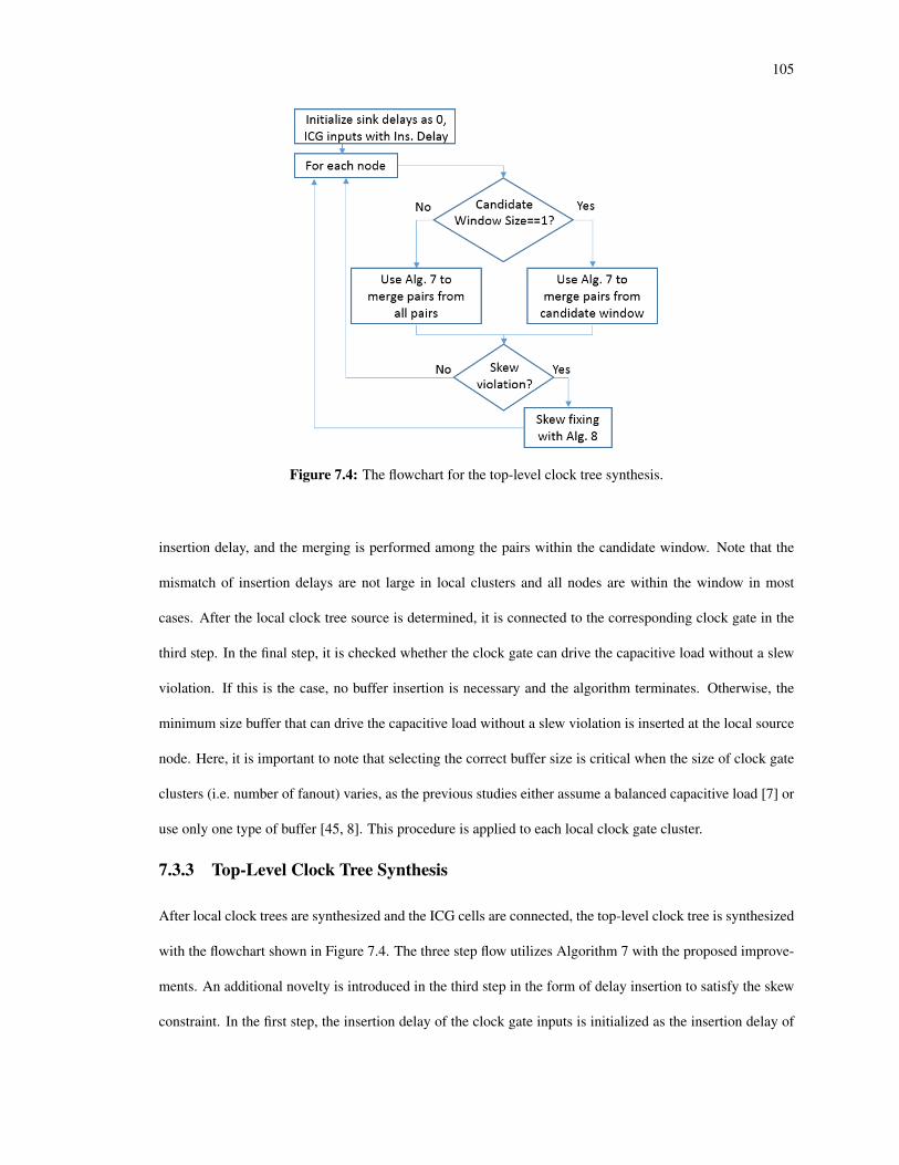
105
Figure 7.4: The flowchart for the top-level clock tree synthesis.
insertion delay, and the merging is performed among the pairs within the candidate window. Note that the
mismatch of insertion delays are not large in local clusters and all nodes are within the window in most
cases. After the local clock tree source is determined, it is connected to the corresponding clock gate in the
third step. In the final step, it is checked whether the clock gate can drive the capacitive load without a slew
violation. If this is the case, no buffer insertion is necessary and the algorithm terminates. Otherwise, the
minimum size buffer that can drive the capacitive load without a slew violation is inserted at the local source
node. Here, it is important to note that selecting the correct buffer size is critical when the size of clock gate
clusters (i.e. number of fanout) varies, as the previous studies either assume a balanced capacitive load [7] or
use only one type of buffer [45, 8]. This procedure is applied to each local clock gate cluster.
7.3.3 Top-Level Clock Tree Synthesis
After local clock trees are synthesized and the ICG cells are connected, the top-level clock tree is synthesized
with the flowchart shown in Figure 7.4. The three step flow utilizes Algorithm 7 with the proposed improve-
ments. An additional novelty is introduced in the third step in the form of delay insertion to satisfy the skew
constraint. In the first step, the insertion delay of the clock gate inputs is initialized as the insertion delay of

106
Algorithm 8 Novel Buffer insertion/Wire snaking to fix skew violations.Input: Buffer library B, skew constraint skewconst , skew factor skew f actor, slew constraint at target node
slewconst(k).Output: List of inserted buffers, and length of required wire snaking.
1: for b in B do2: if Slew(b)< slewconst(k) then3: Insert b4: end if5: end for6: while Dmax(k) - Dmin(k)> skewconst do7: for b in B do8: if Dmax(k) - Dmin(k) - D(b)< skewconst × skew f actor then9: Insert b, found=1
10: end if11: end for12: if found==0 then13: if Inserting max size buffer improves skew then14: Insert max size buffer from B15: else16: Insert wire snaking, break;17: end if18: end if19: end while
their corresponding local trees, and the insertion delay of the non-gated sinks is set to 0. In the second step,
Algorithm 7 is used to construct the top-level clock tree. As different initial delays are defined for each node
in the first step, a prescribed skew approach is considered at the top-level in order to bound overall skew.
Thanks to the candidate window, shown in Figure 7.2, the minimum cost pair is selected within pairs with
small insertion delay differences ( < skewconst ). However, there may be cases, especially at higher levels
in the clock tree, where the insertion delay difference between two nodes is larger than the skew constraint
skewconst , i.e. the candidate merging window contains only one node. In such a case, the minimum cost
pair among all pairs is selected, and a delay insertion methodology, presented in Algorithm 8, is proposed
to bound the overall clock skew in the third step. Algorithm 8 starts with insertion of the minimum size
buffer that can drive the capacitive load without a slew violation (Lines 1-5). The purpose of inserting min-
imum size buffer (that can drive the capacitive load) is the fact that i) higher device resistance of a smaller
size buffer provides a higher delay when driving the same capacitive load, ii) smaller size buffer potentially
consumes less power. After the insertion of the first buffer, the buffer insertion is continued (at the fan-in

107
of the first buffer) with the maximum size buffer that improves the skew (Lines 6-19). Theoretically, this
approach selects the maximum size buffer from the buffer library. However, the solution can be stuck at a
local minimum (that causes an impractically large wire snaking) due to the large delay change caused by the
maximum size buffer, especially at the low swing operation. Thus, a more relaxed approach is proposed here.
The buffer insertion is performed with the following condition: If a buffer can decrease the skew to a margin
closer to the skew constraint (i.e skew f actor× skewconst , skew f actor >1.0), that buffer is inserted (Lines 7-11),
otherwise the maximum size buffer in the library is inserted if it decreases the skew (Line 14). With this flex-
ibility, buffers with different sizes are exploited in order to avoid large wire snaking at the final step, which
possibly results in a slew violation. The buffer insertion is finalized when it is not capable of decreasing the
skew below skewconst , and wire snaking is used as the final step (Line 16). It is important to note here that the
wire snaking is not necessary if the target buffer library has enough granularity of buffer sizes (i.e. small delay
difference in adjacent buffer sizes). In such a case, the skew f actor can also be set to 1.0 as the granularity of
the buffer sizes provides the necessary delay change. If such a library is not present, as in the experimental
setup of this paper, the skew f actor can be set to generate enough margin for the insertion of the minimum
size buffer: The insertion of the minimum size buffer in target library provides ≈70ps delay change, thus the
factor is set to (70-skewconst )/skewconst=1.4 when skewconst is 50ps.
7.3.4 Complexity Analysis
Given N sinks with n clock gate clusters, the algorithm in Figure 7.3 selects one sink in the cluster and
iterates through other ( Nn−1 ) sinks and merges the minimum cost pair. This operation continues until only 1
node is left, which is the input of the clock gate. Thus, the complexity of this algorithm is O(N2
n2 ) per clock
gate cluster, resulting in an overall complexity of O(N2
n ). After clock gates are connected, the algorithm in
Figure 7.4 iterates through each pair within the candidate window, which has n clock gate inputs at the worst
case, therefore, the complexity of this algorithm is O(n2). The total complexity of the proposed methodology
is O(N2
n )+O(n2) when the design has N clock sinks and n clock gate clusters. The worst case complexity of
this algorithm occurs for a non-gated implementation (n=1), which results in an O(N2) complexity, as in the
methodology proposed in Chapter 4. However, considering large portion of clock sinks are gated in today’s
ICs (n >>1), the proposed methodology has a sub-quadratic complexity.

108
Table 7.1: The floorplan size and the total number of clock sinks of benchmark circuits.
Circuits Floorplan Size (µm× µm) Total Number of Sinkss13207 169×166 593s15950 173×169 513s38584 280×272 1274s38417 285×281 1575s35932 289×281 1728
b1 394×381 2838b2 393×387 3002
7.4 Experimental Analysis
7.4.1 Simulation Setup
The proposed algorithm is implemented as a Perl script and the generated netlists are simulated in HSPICE of
Synopsys using 45nm planar CMOS technology from FreePDK library [38] at 1.5 GHz. Five largest circuits
from ISCAS’89 benchmarks are selected with two additional custom blocks (b1 and b2) that are generated
by combining two benchmarks (b1 : s38417+ s38584, b2 : s35932+ s38584) for scalability. The detailed
information about the benchmark circuits used for experimental analysis is presented in Table 7.1. The logic
synthesis of RTL netlists is performed using RTL Compiler of Cadence and the physical placement of DFFs
is performed using SoC Encounter of Cadence. The buffer library has five buffers with various driving
strengths (from X2 to X32), and wire model has per unit values of R=2Ω/µm and C=0.1 f F/µm at the clock
routing layer. The clock skew constraint is set to 50ps (7.5% of clock period) and the slew constraint is set
to 100ps (15% of clock period) at the worst PVT corner (0.9V, 125C, SS transistors). The purpose of using
worst case corner is to maintain the reliability of low swing operation even at the most extreme conditions (i.e.
in lieu of a variation analysis). The low swing voltage level is set to 0.75×Vdd , as it is shown to be the break
point where power savings start leveling in Chapter 2.1.5, which results in 0.675V (0.75×0.9V). In order to
generate a clock gating structure with various fanout sizes, each design is partitioned into a hypothetical 16
grids, and each grid is assigned (or not assigned) to a clock gate as shown in Figure 7.5. The clock gate is
assumed to be placed at the geometrical center of the sinks of each cluster with a 20% activity. Relevant
information is presented for each benchmark circuit in Table 7.2. It is shown that ≈67% of clock sinks are
gated, where each clock gate cluster has a varying number of clock sinks, representing a realistic scenario.

109
Figure 7.5: The clock gate layout assumed for each benchmark circuit. Unlabeled areas contain thenon-gated clock sinks.
The methodology in [45] uses wire snaking to satisfy skew constraints, however, wire snaking is pro-
hibitive when the mismatch between gated and non-gated clock paths are significantly large, as in the ex-
perimental setup of this paper. In order to have a fair comparison against the proposed methodology, the
gated clock tree synthesis methodology [45] is combined with the prescribed skew methodology in [8], as an
additional case for comparison. The quality of results is compared between three cases, which are:
1. a low swing gated clock tree synthesized using the methodology in [45],
2. a low swing gated clock tree synthesized using the methodology in [45], combined with the prescribed
skew methodology in [8], demonstrative of the presumed state-of-the-art as basis for comparison,
3. a low swing gated clock tree synthesized using proposed two-stage approach, with the proposed pre-
scribed skew methodology and the novel delay insertion scheme.
7.4.2 Experimental Results
In Table 7.3, clock power consumption (CP), clock skew (Sk.), and clock slew (Sl.) are compared for the three
cases introduced in Chapter 7.4.1. As shown in Table 7.3, all clock trees implemented with the gated clock
tree synthesis methodology in [45] results in simulation failures, which are caused by large clock slew (due
to excessive wire snaking) that prevents certain nets from switching. On the other hand, when the gated clock

110
Table 7.2: The number of clock sinks at each clock gate cluster and the percentage of gated clock sinksusing the configuration shown in Figure 7.5.
Circuits Number of Sinks in Each Cluster GatingClus. 1 Clus. 2 Clus. 3 Clus. 4 Ptg.
s13207 141 43 165 44 66%s15950 117 25 145 44 65%s38584 291 84 405 87 68%s38417 366 84 527 98 68%s35932 430 109 530 116 69%
b1 588 165 945 199 67%b2 912 164 776 228 69%
Table 7.3: The comparison of clock tree power (CP), clock skew (Sk.) and clock slew (Sl.) of gatedclock tree synthesis methodology in [45], the combination of the gated clock tree methodology in [45]and the prescribed skew methodology in [8], and the proposed gated clock tree synthesis methodology,operating at 0.675V and 1.5 GHz in 45nm technology.
Circuits [45] [45] + [8] Proposed MethodologyCP(mW) Sk.(ps) Sl.(ps) CP(mW) Sk.(ps) Sl.(ps) CP(mW) Sk.(ps) Sl.(ps)
s13207 Simulation Failure 1.72 49.0 95.4 1.06 36.3 91.1s15850 Simulation Failure 1.62 43.6 88.2 0.93 48.4 87.3s38584 Simulation Failure 3.56 46.1 96.3 2.24 43.0 93.7s38417 Simulation Failure 2.77 42.4 87.2 2.41 49.2 89.3s35932 Simulation Failure 2.84 36.5 96.5 2.51 42.5 95.2
b1 Simulation Failure 5.18 48.5 94.2 4.32 48.5 92.9b2 Simulation Failure 4.76 24.1 94.3 4.45 49.7 94.5
Norm. N/A 1.00 <50 <100 0.80 <50 <100
tree synthesis methodology [45] is combined with a prescribed skew approach [8], this combined method-
ology synthesizes feasible clock trees that satisfy the clock skew and slew constraints (50ps and 100ps,
respectively). The proposed methodology satisfies the clock skew and slew constraints, while achieving a
significant 20% power savings against the combined methodology of [45] and [8], thanks to the prescribed
skew approach with the novel delay insertion scheme and the slew-aware buffer insertion. Thus, the pro-
posed methodology not only satisfies tight skew and slew constraints that previous gated clock tree synthesis
methodology [45] is not able to satisfy, it also synthesizes more power-efficient clock trees, compared to the
combination of methodologies in [45] and [8] that obtains a feasible clock tree.

111
Table 7.4: Run time comparison of three methodologies in seconds.
Circuits [45] [45] + [8] Prop. Method.s13207 15 10 13s15950 22 15 19s38584 242 157 197s38417 466 305 389s35932 584 367 458
b1 2356 1588 2095b2 2943 1802 2177
Normalized 1.00 0.64 0.81
7.4.3 Run Time Analysis
Three cases considered in this experimental setup use different methods to select candidate pairs for merg-
ing (line 1 in Algorithm 7), as explained in Chapter 7.3.1. Thus, run times of these three cases are compared
in Table 7.4 to analyze the effect of different selection methods. The methodology in [45] considers all pos-
sible combinations to select pairs, therefore its run time is the highest. The methodology in [8] finds the node
with the minimum insertion delay, and finds its minimum cost pair, therefore the run time is significantly
smaller with 36% improvement when two methodologies are combined. The methodology of this paper se-
lects pairs from the combinations of pairs from the nodes within the candidate window, therefore it considers
a reduced number of combinations compared to [45], which results in 19% run time improvement. The run
time improvement of this paper (19%) is less than the run time improvement through the combination of [45]
and [8] (36%), however, it is shown that the run time of the largest benchmark circuit (that has 3002 DFF
sinks) is a reasonable ≈36 minutes with the proposed methodology.
7.5 Conclusion
In this chapter, a novel low swing gated clock tree synthesis methodology is introduced. The proposed
methodology synthesizes local clock trees for each clock gate cluster while preserving the clock gate loca-
tions, and the top-level clock tree by considering the insertion delay mismatch between the gated and the
non-gated clock sinks. The proposed prescribed skew methodology along with the novel delay insertion and
the slew-aware buffer insertion schemes is shown to be effective to satisfy tight clock skew and slew con-
straints, while achieving significant power savings against the previous work. The proposed methodology is

112
implemented within the IC physical design flow and integrated into an industrial tool, therefore, it is highly
practical for automation purposes.

113
Chapter 8: MULTI-VOLTAGE SINGLE-CLOCK DOMAINCLOCK MESH DESIGN
In multi-voltage designs, a single clock mesh that spans multiple voltage domains is infeasible due to the
incompatibility of voltage levels of the clock drivers on the electrically-shorted mesh, therefore, each voltage
domain requires a separate mesh. The skew among these isolated clock meshes needs to be bounded and
a novel pre-mesh tree synthesis is required to tolerate the impact of PVT variations exacerbated due to the
separation of clock meshes at multiple voltage domains. The case study performed with large ISCAS’89
benchmark circuits operating at 500 MHz in 90nm technology highlights two important results that highlight
the benefits of multi-voltage domain clock mesh design when optimized for a single corner: 1) The multi-
voltage domain clock mesh can achieve 37% lower power with a 10.0ps increase in clock skew over the
single-voltage domain clock mesh, and 2) the multi-voltage domain clock mesh achieves 64.5ps less skew
with a 21% increase in power dissipation over a multi-voltage domain clock tree. When the multi-corner op-
eration is considered for variation-awareness, the multi-voltage domain clock mesh achieves up to 42% lower
power on average with an average skew of 39.0ps, lower than 2% of the clock period, over a typical single-
voltage domain clock mesh. Furthermore, multi-corner-aware multi-voltage domain clock mesh decreases
the global skew across all corners by 190.4ps on average over a multi-voltage domain clock mesh optimized
for a single corner, with a 15% degradation in power consumption necessary for variation-tolerance.
8.1 Introduction
In this chapter, a novel multi-voltage domain clock mesh design methodology is presented. Multi-voltage do-
main clock mesh design has following challenges: First, a single clock mesh is not feasible as its electrically-
shorted mesh wires cannot drive the voltage sinks operating at different voltage levels. Thus, separate meshes
are needed for each domain. Second, clock skew across these voltage domains must be balanced, which is
a challenge that arises due to the isolation of the pre-mesh trees of different voltage domains. Third, the
skew introduced by the PVT variations must be analyzed and bounded considering multiple PVT corners, as
isolated pre-mesh trees in different voltage domains have different tolerances against the PVT variations.

114
The experiments performed on the large circuits of ISCAS’89 benchmarks in 90nm technology at 500 MHz
highlight that the proposed multi-voltage domain clock mesh achieves:
1. 37% power savings with a 10.0ps increase in the skew over the single-voltage domain clock mesh,
2. 21% increase in power consumption with a 64.5ps decrease in the skew over the multi-voltage domain
clock tree,
when optimized for a single PVT corner.
Literature on clock meshes focuses on design methodologies for mesh reduction and optimization, and
ignores multi-corner analysis, as the ubiquitous shorting of branches provides remarkable robustness under
PVT variations. However, this assumption only holds true for a traditional, single-voltage domain clock mesh.
When a multi-voltage single-clock domain design is considered, a clock network built with the mesh topology
becomes uncharacteristically susceptible to PVT variations. This susceptibility emerges as a multi-voltage
domain clock mesh is constructed with disjoint pre-mesh trees and meshes, each synchronizing an individual
voltage domain. Hence, a novel methodology is necessary to synthesize a variation-tolerant, power-efficient
multi-voltage domain clock network. When the multi-corner improvements are considered, there are two
additional benefits:
1. Proposed multi-corner-aware multi-voltage domain clock mesh achieves up to 42% lower power across
three PVT corners with a worst case skew of 39.0ps on average, which resides in the 2% budget of the
clock period.
2. Proposed improvements achieve 190.4ps lower skew in average and a much tighter slew compared to
optimizing multi-voltage domain clock mesh design at only one PVT corner, with a 15% degradation
in the power consumption at that corner.
8.2 Methodology
A novel methodology to synthesize a mesh-based clock distribution network in a multi-voltage design flow
is proposed. The steps of the proposed methodology are:
1. the physical placement in each voltage domain is performed using standard EDA tools,

115
2. a uniform mesh size is selected for each voltage domain considering the skew constraints in the domain,
3. pre-mesh drivers are placed at each intersection, and sized considering the slew constraints,
4. pre-mesh tree is synthesized iteratively to bound the global skew.
In clock mesh design, uniform clock mesh grids are preferred to place the mesh wires between power
rails to prevent crosstalk. Thus, uniform clock mesh grids are considered in this study. In the typical single-
voltage domain clock mesh design, shown in Figure 2.14(a), the mesh wires are directly connected to the
sinks and the mesh is driven by a pre-mesh tree. For the multi-voltage domain clock mesh, on the other
hand, each domain needs its own clock mesh. To that end, local meshes are placed at each voltage domain
with their own pre-mesh trees. Then, the local roots of each voltage domain are connected to a master root
through level shifters, as shown in Figure 2.14(b). The mesh size selection, buffer driver selection and sizing,
and the pre-mesh tree synthesis procedures are presented in Chapter 8.2.1, Chapter 8.2.2 and Chapter 8.2.3,
respectively. The methodologies presented in Chapter 8.2.1 and Chapter 8.2.2 are simple algorithms that do
not define the novelty of this work but complement the design flow. Note that any alternative method for
mesh size selection and mesh driver sizing can be seamlessly integrated, which demonstrates the practicality
of the proposed method for automation purposes.
8.2.1 Mesh Size Selection
The clock skew within a voltage domain is directly related to the density of the clock mesh. With a sparser
mesh, the distance from the intersection (i.e. buffer locations) to the mesh connection point of a stub wire,
and the distance from the sink flip-flop to the mesh connection point increases, both of which are contribut-
ing to clock skew. On the other hand, a denser mesh increases the mesh capacitance, which increases the
power consumption. To that end, the smallest N×N mesh size is targeted in each voltage domain by a simple
exhaustive search by increasing N until the skew becomes less then a user-defined threshold. If prior informa-
tion is available on a suitable clock mesh size or depending on the floorplan size, a larger initial mesh size N
can be selected to start the iterations. This procedure is presented in Algorithm 9.

116
Algorithm 9 Mesh Size SelectionInput: Sink locations, skew constraint skewi
const for each voltage domain i.Output: The mesh size Ni for each voltage domain i.
1: for Each voltage domain i do2: Initialize Ni, e.g. Ni=13: Calculate skewi
max4: while skewi
max > skewiconst do
5: Ni = Ni + 16: Update skewi
max7: end while8: end for9: Return Ni for each domain i
Algorithm 10 Pre-mesh Driver SelectionInput: Mesh size for each voltage domain i, buffer library, slew constraint slewconst .Output: The size of buffers at each intersection.
1: for Each voltage domain i do2: Place minimum buffer at each intersection3: Calculate slewmax4: while slewi
max > slewconst do5: Replace all buffers with the next larger buffer cell in the library6: Update slewi
max7: end while8: end for9: Return the selected driver for each domain i
8.2.2 Pre-mesh Driver Selection
After the mesh size is selected, the pre-mesh drivers are placed at each intersection. A simple heuristic is
used to select these buffers. First, minimum size buffers are placed at each intersection, and the buffer sizes
are iteratively increased to satisfy the slew constraint. The slew constraint is typically set to 5% of the clock
period in high performance ICs. To that end, the user-defined slew constraint, slewconst , is selected as 5% of
the clock period, although it can be set to another value depending on the performance requirements. Note
that this constraint may be degraded by the synthesized pre-mesh tree in the following step, yet the slew target
needs to be selected in this stage as it is used as a guide that drives the pre-mesh tree synthesis stage. In the
pre-mesh driver selection procedure, all the buffers are sized up at the same time with an identical scale for
the sake of simplicity. This procedure is shown in Algorithm 10.

117
Algorithm 11 Cross Domain Delay MatchingInput: Mesh size of each domain, assigned voltage for each domain, buffer library for each domain, slew
constraint slewconst , cross domain skew constraint skewcrossconst .
Output: Pre-mesh tree for each domain i.1: Place the (n-1)st level of the pre-mesh tree using slewconst2: Calculate the maximum delay delayi
max for each voltage island i3: while max∀i(delayi
max)−min∀i(delayimax)> skewcross
const do4: K = min∀i(delayi
max) and k as the corresponding domain5: Set M = max∀i(delayi
max)6: while K < M− skewcross
const/2 do7: Add a minimum buffer to k8: Update K = delayk
max9: end while
10: if K > M+ skewcrossconst/2 then
11: Remove the last-added buffer from k12: Update K = delayk
max13: end if14: while K < M do15: Increase the size of the minimum buffer in domain k to the one larger buffer in the library16: Update K = delayk
max17: end while18: end while19: Return the pre-mesh tree for each domain i
8.2.3 Pre-mesh Tree Synthesis
Pre-mesh tree synthesis is the most critical step of the multi-voltage domain clock mesh design flow, as the
insertion delay at all voltage domains must be matched to bound clock skew. Moreover, as the slew of the
clock mesh (Chapter 8.2.2) is not completely independent from the pre-mesh tree, it should not be degraded
when building the pre-mesh tree.
In the multi-voltage design flow, standard EDA tools cannot match the insertion delays of the pre-mesh
trees driving clock meshes that belong to different voltage domains. In this study, an iterative algorithm is
proposed to accomplish this task. In the algorithm, the pre-mesh tree is built up iteratively without degrading
the slew at the clock sinks until the skew across all voltage domains becomes less than a user-specified
threshold. This procedure is shown in Algorithm 11.
In Algorithm 11, first, the (n-1)st level of the pre-mesh tree is synthesized considering the slew con-
straints (line 1). The purpose is not to degrade the slew set in Algorithm 10 more than 20% (note that overall
slew limit is determined as a combination of the slew constraint slewconst in Chapter 8.2.2 and this degra-

118
dation margin in Algorithm 11). Next, the insertion delay of each clock sink is calculated to observe the
delay differences among the voltage domains (line 2). The skew among the clock sinks within the same
voltage domain is very small. Thus, the maximum insertion delay in each voltage domain is selected as
the common insertion delay of that domain without loss of generality. In line 3, the iterations start in a
while loop until the difference between the maximum and the minimum insertion delays across all voltage
domains is less than the user-defined cross-domain skew threshold skewcrossconst . The voltage domain with the
minimum insertion delay is determined and labeled as k, and the minimum and the maximum insertion delays
across all voltage domains are labeled as K and M, respectively (lines 4-5). An iterative minimum size buffer
insertion is performed to voltage domain k until the delay K of this domain exceeds a minimum threshold (M-
skewcrossconst /2) (lines 6-9). If K also exceeds the maximum threshold (M+skewcross
const /2), the last-added buffer is
removed from K (lines 10-13). In line 14, the delay of the voltage domain, K is compared to M. If it is smaller
than M, K is increased gradually by increasing the buffer sizes in voltage domain k starting from the buffer
with the minimum size, until it exceeds M (lines 14-17). After this step, the same procedure is followed on
the voltage domain with the second smallest insertion delay. The iterations terminate when the global skew
is less than the user-specified threshold. In this procedure, the solution quality depends on the user-defined
cross-domain skew threshold skewcrossconst , as it is the key parameter that controls the trade-off between the skew
and the power consumption (tight skew constraints increases the number of buffers inserted). The global skew
constraint is typically 2% of the clock period. To that end, the user defined global skew constraint skewcrossconst
is selected as the 2% of the clock period in this study, although it can be set to a different value depending on
the performance requirements.
8.3 An Improved Methodology for Variation-Awareness
An improved methodology is presented to consider multiple PVT corners for multi-voltage domain clock
mesh design. By considering multiple PVT corners simultaneously, variation-tolerance is targeted. Given
an initial placement and the mesh size (determined in Chapter 8.2.1), the steps of the modified multi-corner-
aware methodology are:
1. placement of pre-mesh drivers at each intersection, and their sizing considering the slew constraints at
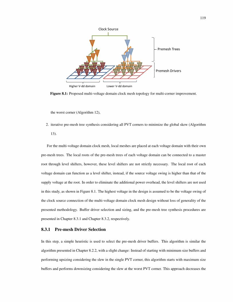
119
c c
Clock Source
Premesh Trees
Premesh Drivers
Higher V-dd domain Lower V-dd domain
Figure 8.1: Proposed multi-voltage domain clock mesh topology for multi-corner improvement.
the worst corner (Algorithm 12),
2. iterative pre-mesh tree synthesis considering all PVT corners to minimize the global skew (Algorithm
13).
For the multi-voltage domain clock mesh, local meshes are placed at each voltage domain with their own
pre-mesh trees. The local roots of the pre-mesh trees of each voltage domain can be connected to a master
root through level shifters, however, these level shifters are not strictly necessary. The local root of each
voltage domain can function as a level shifter, instead, if the source voltage swing is higher than that of the
supply voltage at the root. In order to eliminate the additional power overhead, the level shifters are not used
in this study, as shown in Figure 8.1. The highest voltage in the design is assumed to be the voltage swing of
the clock source connection of the multi-voltage domain clock mesh design without loss of generality of the
presented methodology. Buffer driver selection and sizing, and the pre-mesh tree synthesis procedures are
presented in Chapter 8.3.1 and Chapter 8.3.2, respectively.
8.3.1 Pre-mesh Driver Selection
In this step, a simple heuristic is used to select the pre-mesh driver buffers. This algorithm is similar the
algorithm presented in Chapter 8.2.2, with a slight change: Instead of starting with minimum size buffers and
performing upsizing considering the slew in the single PVT corner, this algorithm starts with maximum size
buffers and performs downsizing considering the slew at the worst PVT corner. This approach decreases the

120
Algorithm 12 Multi-Corner-Aware Pre-mesh Driver SelectionInput: Mesh size for each voltage domain i, buffer library, slew constraint slewconst .Output: The sizes of each pre-mesh driver buffers.
for Each voltage domain i doPlace maximum size buffer at each intersectionCalculate slewi
maxwhile slewi
max < slewconst doReplace all buffers with the next smaller buffer cell in the libraryUpdate slewi
maxend while
end forReturn the selected driver for each domain i
number of iterations because satisfying the slew constraint at the worst corner requires larger sizes of buffers,
compared to the corner that single corner-optimized methodology considers. This algorithm is shown in
Algorithm 12.
8.3.2 Multi-Corner-Aware Pre-mesh Tree Synthesis
A novel methodology that synthesizes a pre-mesh tree to optimize the global skew considering all PVT
corners simultaneously is presented. This stage also considers the slew at the sinks, not to degrade the slew
more than an allowed margin within the slew budget, as the maximum slew (Chapter 8.3.1) of the design is
not completely independent from the pre-mesh tree.
It is important to note the significance of the proposed skew-and-slew budgeted multi-corner-aware, multi-
voltage domain clock mesh design methodology within the current state of the art clock mesh design automa-
tion: In the multi-voltage design flow, standard EDA tools cannot match the insertion delays of the pre-mesh
trees driving clock meshes that belong to different voltage domains even in a single corner, as stated in Chap-
ter 8.2. In this study, an iterative algorithm is proposed to accomplish this task at all PVT corners, expanding
the applicability of the methodology presented in Chapter 8.2.3. In the algorithm, the pre-mesh tree is syn-
thesized iteratively, until the lowest global skew across all corners is achieved. This procedure is shown in
Algorithm 13.
In this algorithm, first, the (n-1)st level of the pre-mesh tree is synthesized with the maximum size buffers
in an N×N topology. The iterations starts (generically) with N=1 (line 1), and it is increased by 1 (also

121
Algorithm 13 Multi-Corner-Aware Multi-Voltage Domain Pre-mesh Tree SynthesisInput: Pre-mesh drivers for each domain, assigned voltage for each domain, buffer library for each domain
i and each corner c, slew constraint slewconst .Output: Pre-mesh tree for each domain i.
1: Set N = 12: while slewmax > slewconst + slewmargin do3: Place N × N max size buffers at the (n-1)st level of each domain i4: N = N + 15: end while6: if max insertion delay is in the same domain for all cases then7: while max insertion delay is still at the same domain j do8: Add a max size buffer of that voltage domains other than j9: end while
10: end if11: currskew = max∀c(max∀i(delayi
max) - (min∀i(delayimin))
12: prevskew = T13: while k j < num o f levels j do14: Downsize the k-th level of the max insertion delay domain j15: prevskew = currskew16: currskew = max∀c(max∀i(delayi
max) - (min∀i(delayimin))
17: if currskew > prevskew then18: Undo that step, mark k-th level as done19: k j = k j + 120: end if21: end while22: while currskew > prevskew do23: Add parallel buffers at the max insertion delay domain at the first level24: prevskew = currskew25: currskew = max∀c(max∀i(delayi
max) - (min∀i(delayimin))
26: end while
generically) at each iteration until the slew constraint with the degradation margin is met at all corners (lines 2-
5). Then, the insertion delays are measured to see if the maximum insertion delay path is in the same voltage
domain for all cases. As shown in Chapter 2.2.3, optimizing the skew across all corners simultaneously
requires an early arrival of the clock signal in the lower voltage domain at the best case so as to have a
balanced skew at the worst case, and for the skew budget to be lower. Hence, having the maximum insertion
delay in the same voltage domain is an undesired case. This undesired case is avoided with a maximum size
buffer insertion in the next level of each voltage domain other than the voltage domain with the maximum
insertion delay (lines 6-10). The purpose of selecting maximum size buffers in this stage is the fact that having
less number of levels in the pre-mesh tree with larger size buffers is more variation-tolerant than having more
number of levels with smaller buffers. Buffer insertion stage ends when the maximum insertion delay paths

122
are no longer encountered in the same voltage domain for different corners. The buffer insertion stage is
succeeded by the buffer sizing stage. In the buffer sizing stage, the buffers are downsized starting from the
first level of the voltage domain whose maximum insertion delay path sets the global skew (line 14). If
downsizing improves the skew, that step is performed. Otherwise, that step is undone and that level is marked
as “done” (lines 17-20). Downsizing continues with the voltage domain with the second highest insertion
delay and finalizes when all levels of all voltage domains are marked as “done”. After this stage, pruning
stage starts. In this last stage, the number of levels or the sizes of the buffers are unchanged, but parallel
buffers of the same sizes are added at the first level of the voltage domain with the maximum insertion delay
iteratively as long as the global skew is improved (lines 22-25). The algorithm is an heuristic and does not
guarantee an optimal solution, yet it is empirically shown to be effective. The algorithm visits each voltage
domain constant number of times, and simulates only for the best and the worst corners. Thus, the complexity
is O(n) with n voltage domains and m PVT corners.
8.4 Experimental Analysis
The simulation setup of the presented experimental analysis is presented in Chapter 8.4.1. In Chapter 8.4.2,
the effectiveness of the multi-voltage domain clock mesh topology against existing topologies implemented
by industrial design tools optimized for a single PVT corner is shown. The effectiveness of the improved
multi-corner-aware methodology of Chapter 8.3.2, which expands the applicability of multi-voltage domain
clock mesh topology with variation-awareness, is presented in Chapter 8.4.3.
8.4.1 Simulation Setup
The proposed methodologies in Chapter 8.2 and Chapter 8.3 are implemented in Tcl in order to inter-operate
with standard EDA tools. Similar to most standard cell libraries, the selected SAED 90nm EDK Library [58]
has two voltage levels, a high voltage at 1.2V and a low voltage at 0.8V. Consequently, the number of voltage
domains in this study is two. The RTL netlists are synthesized using Design Compiler of Synopsys and the
placement of the circuits are performed using IC Compiler of Synopsys. The skew and the power analyses
are performed using CustomSim XA simulator of Synopsys at the SPICE accuracy level. Due to the tight
slack constraints at the domain that operates at 0.8V, 500 MHz is selected as the operating frequency. The

123
user-defined constraints are selected as follows: The skew inside a voltage domain skewiconst is selected as
2ps for both voltage domains to keep the intra-domain skew small. The maximum slew slewconst is selected
as 100ps, with a degradation margin allowance in pre-mesh tree synthesis of 20% totaling to a slew budget of
120ps. The cross domain (global) skew skewcrossconst is selected as 40ps, as explained Chapter 8.2.3. In order to
verify the variation-tolerance, the multi-corner analysis is performed at 3 different PVT corners:
1. Best Corner (BC): V=1.1×Vdd , T=-40C, fast transistors (FF)
2. Nominal Corner (NC): V=Vdd , T=25C, typical transistors (TT)
3. Worst Corner (WC): V=0.9×Vdd , T=125C, slow transistors (SS)
that are available in the target technology library.
8.4.2 Results for Single-Corner Analysis
Within the two voltage domains, two of the largest circuits of ISCAS’89 benchmarks, s35932 and s38417,
are placed. The larger design s35932, with 1728 sinks, is supplied with 0.8V and the smaller s38417, with
1564 sinks, is supplied with 1.2V without loss of generality. In order to compare the quality of results to the
standard single-voltage domain clock mesh and multi-voltage domain clock tree, the following procedure is
performed: A single-voltage domain clock mesh is synthesized by selecting the mesh size and the pre-mesh
drivers using the proposed methods given in Chapter 8.2.1 and Chapter 8.2.2 for consistency. Then, the
pre-mesh tree is synthesized using IC Compiler. Also, a dual-voltage domain clock tree is synthesized and
optimized by IC Compiler of Synopsys.
The synthesized dual-voltage domain clock mesh, single-voltage domain clock mesh and the dual-voltage
domain clock tree are shown in Figure 8.2, Figure 8.3 and Figure 8.4, respectively. The proposed methodol-
ogy outputs a 10×10 mesh for both of the partitions and selects NBUFFX4 from the SAED 90nm library as
the pre-mesh driver. The maximum slew at the clock sinks in the proposed dual-voltage domain clock mesh
design (shown in Figure 8.2) is 108.7ps, which is within the allowed margin of 120ps. The experimental
results show that the proposed multi-voltage domain clock mesh can reduce the power dissipation by 37%
compared to the single-voltage domain clock mesh (shown in Figure 8.3), with a slight increase in clock
skew from 0.9ps to 10.9ps. Compared to the dual-voltage domain clock tree synthesized and optimized by IC
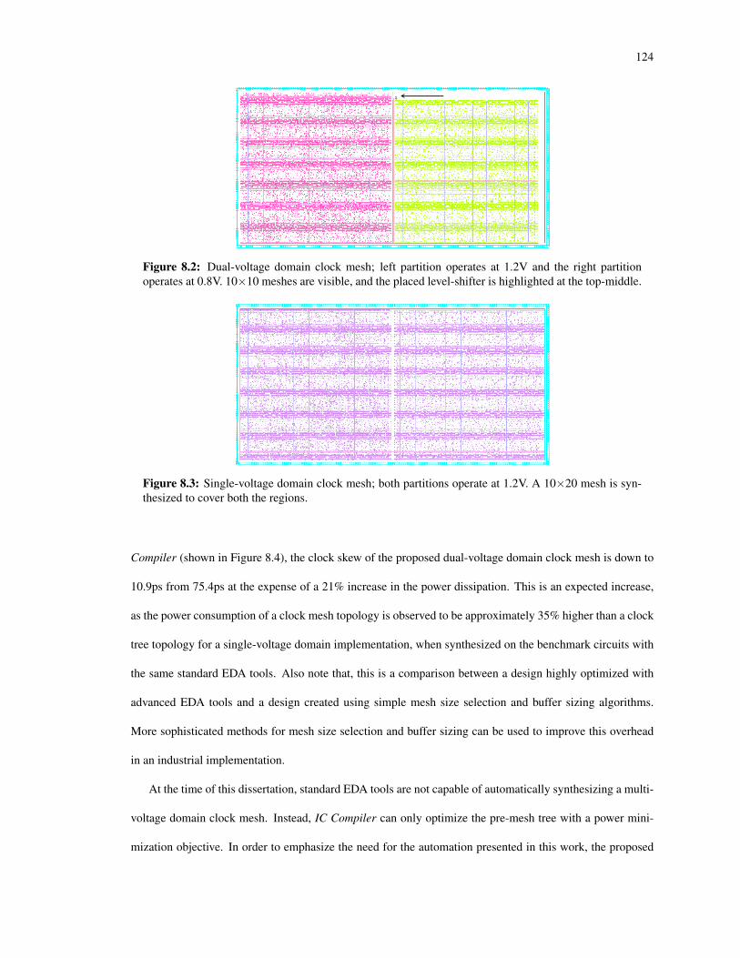
124
Figure 8.2: Dual-voltage domain clock mesh; left partition operates at 1.2V and the right partitionoperates at 0.8V. 10×10 meshes are visible, and the placed level-shifter is highlighted at the top-middle.
Figure 8.3: Single-voltage domain clock mesh; both partitions operate at 1.2V. A 10×20 mesh is syn-thesized to cover both the regions.
Compiler (shown in Figure 8.4), the clock skew of the proposed dual-voltage domain clock mesh is down to
10.9ps from 75.4ps at the expense of a 21% increase in the power dissipation. This is an expected increase,
as the power consumption of a clock mesh topology is observed to be approximately 35% higher than a clock
tree topology for a single-voltage domain implementation, when synthesized on the benchmark circuits with
the same standard EDA tools. Also note that, this is a comparison between a design highly optimized with
advanced EDA tools and a design created using simple mesh size selection and buffer sizing algorithms.
More sophisticated methods for mesh size selection and buffer sizing can be used to improve this overhead
in an industrial implementation.
At the time of this dissertation, standard EDA tools are not capable of automatically synthesizing a multi-
voltage domain clock mesh. Instead, IC Compiler can only optimize the pre-mesh tree with a power mini-
mization objective. In order to emphasize the need for the automation presented in this work, the proposed

125
Figure 8.4: Dual-voltage domain clock tree; left partition operates at 1.2V and the right partition oper-ates at 0.8V. The placed level-shifter is highlighted at the top-middle.
Table 8.1: The power and the skew trade-off of the proposed methodology against clock networkssynthesized by IC Compiler (ICC).
Clock Networks Skew (ps) Power (mW) ImprovementSkew (ps) Power
Proposed dual-voltage mesh 10.9 67.23 - -Dual-voltage tree synthesized by ICC 75.4 55.60 64.5 -21%Single-voltage mesh optimized by ICC 0.9 106.96 -10.0 37%Dual-voltage mesh optimized by ICC 229.6 61.96 218.7 -9%Single-voltage tree synthesized by ICC 73.8 79.51 62.9 15%
multi-voltage domain clock mesh design is compared to the multi-voltage domain clock mesh design whose
pre-mesh tree is optimized in IC Compiler. As automated tools cannot match the insertion delay at different
voltage domains as necessitated by the proposed multi-voltage domain clock mesh implementation, the EDA
tool optimizes the power with a larger delay mismatch. Proposed methodology achieves substantially better
skew at 10.9ps (less than 1% of the clock period) compared to 229.4ps with a 9% increase in the power
dissipation. In order to highlight the power savings of the proposed methodology, it is also compared with
a single-voltage domain clock tree, synthesized and optimized by IC Compiler. The proposed method dissi-
pates 18% less power compared to the single-voltage domain clock tree with a skew of 73.8ps. The power and
the skew trade-off of the proposed dual-voltage domain clock mesh compared to the other implementations
synthesized by IC Compiler (ICC) is summarized in Table 8.1.

126
Table 8.2: Created benchmark circuits.
0.8V Domain 1.2V DomainBenchmark 1 s35932 s38417Benchmark 2 s38417 s35932Benchmark 3 s35932 s38584Benchmark 4 s38584 s35932
8.4.3 Results for Multi-Corner Analysis
For testing purposes, four benchmark circuits are created by placing different combinations of the three largest
circuits of ISCAS’89 benchmarks, s35932, s38417 and s38584 within two voltage domains. These combina-
tions are shown in Table 8.2. In order to compare the quality of results to the standard single-voltage domain
clock mesh and the single-corner-aware methodology introduced in Chapter 8.2, the following procedure is
performed: A single-voltage domain clock mesh is synthesized using IC Compiler in the multi-corner mode,
and its pre-mesh drivers are sized using the proposed method given in Chapter 8.3.1 for consistency. The
single-corner-aware methodology introduced in Chapter 8.2 is also presented on the same circuits to compare
to the improved multi-corner-aware algorithm. The mesh size is selected as 10×10, similar to Chapter 8.4.2,
to have a fair comparison.
The pre-mesh buffer sizing (Chapter 8.3.1) and the pre-mesh tree synthesis stage (Chapter 8.3.2) of the
improved multi-corner-aware methodology takes, respectively, two and nine iterations at most to converge.
The experimental results are shown in Table 8.3 and Table 8.4. Recall that the contemporary practical ob-
jective in clock distribution network design is to optimize power within a given skew/slew bound. It is
visible from Table 8.4, that a single-voltage domain clock mesh is the best in terms of clock skew, as the
single-voltage domain clock mesh (famously) has a very high variation-tolerance. The important contribu-
tion of this methodology is that, when multi-voltage designs are implemented, the clock mesh can preserve its
variation-tolerance while reducing the power dissipation through multi-voltage design. The improved multi-
corner-aware methodology can achieve up to 42% power savings compared to a single-voltage domain clock
mesh. The skew increases from 1.7ps to 39.0ps on average, as shown in Table 8.4, yet it is still less than
2% of the clock period. In comparison, the single-corner-aware algorithm introduced in Chapter 8.2 does not

127
2% 5% 10%
Figure 8.5: Skew comparison of single-voltage mesh (SV Mesh) synthesized by IC Compiler (ICC),single-corner-aware multi-voltage clock mesh methodology (SCAMV Mesh), and improved multi-corner-aware multi-voltage mesh methodology (IMCAMV Mesh) vs. typical skew budgets (2%, 5%and 10% of clock period).
Table 8.3: Power comparison of improved multi-corner-aware multi-voltage clock mesh methodol-ogy (IMCAMV Mesh) over single-voltage domain mesh (SV Mesh) synthesized by IC Compiler (ICC)and single-corner-aware multi-voltage clock mesh methodology (SCAMV Mesh) at best corner (BC),nominal corner (NC), and worst corner (WC) in mW.
Circuits SV Mesh synth. by ICC SCAMV Mesh IMCAMV MeshBC NC WC BC NC WC BC NC WC
Benchmark 1 467.64 112.69 201.89 272.56 66.52 137.90 304.19 82.97 132.72Benchmark 2 502.04 128.33 220.41 219.09 80.28 148.54 254.88 95.96 140.25Benchmark 3 385.19 93.17 178.90 197.55 48.34 104.18 231.41 64.51 102.70Benchmark 4 434.58 106.73 184.59 212.60 72.29 145.62 239.84 88.26 132.65
Avg. % Improvement 49% 40% 32% 42% 25% 35%
satisfy the 5% (or 10%) skew budget at 229.5ps on average, which is approximately 11% of the clock period,
as highlighted in Figure 8.5. It is concluded that the single-corner-aware algorithm introduced in Chapter 8.2
is useful in demonstrating the feasibility of a multi-voltage domain clock mesh topology, yet it is intolerant to
PVT variations. The improved multi-corner-aware methodology synthesizes effective multi-voltage domain
clock mesh designs across multiple PVT corners, therefore, it complements the study.
It is reported in Table 8.3 that the power dissipation in the multi-voltage domain clock mesh is much lower
compared to a single-voltage domain clock mesh. The total power savings on the multi-voltage circuit will
be even higher considering the additional savings on the logic, which are not reported here (as total power
savings depend on the particular voltage domain partitioning technique and may sway the results). The
power savings of the improved multi-corner-aware methodology has 15% degradation in power consumption

128
Table 8.4: Skew comparison of improved multi-corner-aware multi-voltage clock mesh methodol-ogy (IMCAMV Mesh) over single-voltage domain mesh (SV Mesh) synthesized by IC Compiler (ICC)and single-corner-aware multi-voltage clock mesh methodology (SCA Mesh) at best corner (BC), nom-inal corner (NC), and worst corner (WC) in ps, overall skew is bold.
Circuits SV Mesh synth. by ICC SCAMV Mesh IMCAMV MeshBC NC WC BC NC WC BC NC WC
Benchmark 1 1.3 1.0 0.6 228.0 21.1 177.3 40.2 20.2 28.8Benchmark 2 1.5 2.7 4.0 227.4 21.6 178.7 38.9 18.5 30.9Benchmark 3 2.5 1.9 1.2 229.6 20.6 179.2 30.3 10.0 39.1Benchmark 4 1.6 1.3 0.8 232.8 16.4 170.1 30.3 10.1 38.0Avg. Skew 1.7 229.5 39.0
Degradation -227.7 -37.3
in the nominal case over the single-corner-aware methodology, as optimization at multiple PVT corners is
considered. The 15% power degradation, therefore, is not a penalty but a necessity to achieve a slew and a
skew constrained design. The slew constraint in single-corner-aware methodology is 120ps in the nominal
case, but it is observed to be 240.4ps in the worst case, which requires an extravagant 12% slew budget. In
comparison, the worst case slew budget in the improved multi-corner-aware methodology is 120ps, which is
satisfied at 108.4ps, 5% of the clock period, in the worst case. The degradation in power savings is 7% in the
best case corner, and there is a 3% improvement in power savings in the worst case corner. These improved
power consumption profile at the best and the worst corner highlights the multi-corner optimization objective
of the improved multi-corner-aware methodology.
8.5 Conclusion
Two novel methodologies are proposed to synthesize variation-tolerant, multi-voltage, single-clock domain
clock meshes for high performance ICs. The single-corner-aware methodology highlights the feasibility of
multi-voltage domain clock mesh design by demonstrating the limitations of industrial tool flows in clock
mesh synthesis for multi-voltage designs. Improved multi-corner-aware methodology enables a variation-
tolerant multi-voltage domain clock mesh synthesis for improved applicability. Slew-and-skew budgeted
pre-mesh tree synthesis considers all PVT corners for high practicality. It is shown in the experimental results
that multi-voltage domain clock mesh topology is a good alternative to clock tree topology to satisfy tight
clock skew and slew constraints with limited penalty in power consumption. In this work, simple algorithms

129
are used for mesh size and pre-mesh driver size selection within voltage domains to emphasize the elegance of
multi-voltage domain clock mesh topology and the multi-corner-aware pre-mesh tree synthesis. Thus, these
methodologies can easily be combined with existing clock mesh optimization and buffer sizing algorithms
for improved results and a wider practical applicability.

130
Chapter 9: CONCLUSIONS AND FUTURE DIRECTIVES
Design automation of voltage-scaled clock distribution networks is an active research topic as the increased
density of current ICs requires low power methods to limit power density and meet tight power budgets. In
this dissertation, novel algorithms are proposed to synthesize low swing clock trees to achieve higher timing
performance while preserving power savings of low swing clocking. Furthermore, a novel topology, multi-
voltage single-clock domain clock mesh, is introduced in order to achieve significant power savings while
preserving the high timing performance of clock mesh topology. The conclusions of this dissertation are
presented in Chapter 9.1, and the future directives on voltage-scaled clock distribution networks are presented
in Chapter 9.2.
9.1 Conclusions
The conclusions for low swing clock trees and multi-voltage single-clock domain clock mesh are presented
in Chapter 9.1.1 and Chapter 9.1.2, respectively.
9.1.1 Conclusions on Low Swing Clock Trees
In this dissertation, several algorithms are introduced in order to i) show the feasibility of low swing clock
trees, ii) develop automated flows for low swing clocking to achieve significant power savings at the same
performance constraints, iii) extend the applicability of low swing clocking to FinFET technology, iv) present
slew-driven algorithms that achieves additional power savings in the future technology nodes, v) facilitate
clock gating within the low swing clocking flow to extend the applicability of low swing clocking.
The feasibility study presented in Chapter 3 has shown that low swing clock trees can be enabled through
in-place buffer sizing on legacy full swing clock trees with limited degradation on timing and flip-flop power
consumption.
The automated flow presented in Chapter 4 has shown that a slew-aware low swing clock tree synthesis
combined with a low swing flip-flop design can satisfy the same timing constraints as its full swing coun-
terpart, while achieving significant power savings. It is also shown that the different targets on the power-

131
performance trade-off curve can be achieved at different frequency targets, across different transistor and
interconnect technologies.
The FinFET-based low swing clocking flow in Chapter 5 has shown that the unique properties of FinFET
technology (in reducing leakage power and having smaller gate delay) make low swing clocking a perfect
candidate for significant power savings. It is also shown that the combined improvements of FinFET tech-
nology and the proposed design flow enables frequency scaling with the same power target, and significant
power savings with the same frequency target.
The slew-driven clock tree synthesis algorithm presented in Chapter 6 has shown that focusing on clock
slew rather than clock skew is more beneficial for the future technology nodes where the interconnect
resistance is more significant than device resistance. Slew-driven approach has outperformed traditional
skew/delay-driven approaches in the low voltage and high frequency implementations, providing additional
power savings for low swing clocking at high performance ICs.
The low swing gated clock tree synthesis algorithm presented in Chapter 7 has introduced an improved
algorithm to facilitate clock gating within low swing clocking flow. It is shown that this algorithm can
successfully combine the power savings of clock gating and low swing clocking, while satisfying the same
timing constraints.
9.1.2 Conclusions on Multi-Voltage Single-Clock Domain Mesh
The multi-voltage single-clock domain clock mesh topology is introduced in Chapter 8. This dissertation
is the first work that shows that multi-voltage clock mesh topology is effective to preserve the high tim-
ing performance of clock mesh topology while achieving significant power savings. It is also shown that
the multi-corner-aware algorithm synthesizes multi-voltage domain clock meshes that are effective across
different PVT corners.
9.2 Future Directives
In this dissertation, various algorithms has been proposed to synthesize voltage-scaled clock distribution
networks that satisfies tight timing constraints while achieving significant power savings. In this section,
future studies are proposed in order to improve the effectiveness of voltage-scaled clock distribution networks.

132
9.2.1 Future Directives on Low Swing Clock Trees
The applicability of low swing clock trees can be extended through additional improvements. One possible
improvement is to perform a low swing clock tree and low swing voltage grid co-synthesis. With this co-
synthesis, not only the low swing clock tree is optimal, but also the power grid for the target voltage swing
is optimized for the low swing clock tree. This co-synthesis approach helps reduce the negative effects of
voltage supply variation, and helps compute an optimal voltage swing that considers both clock tree and the
low swing power grid.
9.2.2 Future Directives on Multi-Voltage Single-Clock Domain Clock Mesh
One possible future directive to improve multi-voltage single-clock domain clock distribution networks is to
study dynamically scaled voltage domains, rather than pre-assigned static voltage levels. This implementation
requires a multi-corner multi-mode (MCMM) algorithm that considers not only multiple PVT corners but also
multiple modes of voltage assignment. This algorithm will extend the applicability of multi-voltage single-
clock domain clock mesh to current microprocessors where dynamic voltage and frequency scaling (DVFS)
is a norm.

133
Bibliography
[1] A. Abdelhadi, R. Ginosar, A. Kolodny, and E. G. Friedman. Timing-driven variation-aware nonuni-form clock mesh synthesis. In Proceedings of the ACM International Great Lakes Symposium on
VLSI (GLSVLSI), pages 15–20, May 2010.
[2] F. H. A. Asgari and M. Sachdev. A low-power reduced swing global clocking methodology. IEEE
Transactions on Very Large Scale Integration (TVLSI) Systems, 12(5):538–545, May 2004.
[3] C. Auth and et al. A 22nm high performance and low-power CMOS technology featuring fully-depletedtri-gate transistors, self-aligned contacts and high density MIM capacitors. In Proceedings of the IEEE
Symposium on VLSI Technology (VLSIT), pages 131–132, Jun. 2012.
[4] H. B. Bakoglu. Circuits, Interconnects, and Packaging for VLSI. Addison-Wesley, 1990.
[5] K. D. Boese and A. B. Kahng. Zero-skew clock routing trees with minimum wirelength. In Proceedings
of the IEEE International ASIC Conference and Exhibit, pages 17–21, 1992.
[6] Y. Cai, C. Deng, Q. Zhou, H. Yao, F. Niu, and C. N. Sze. Obstacle-avoiding and slew-constrained clocktree synthesis with efficient buffer insertion. IEEE Transactions on Very Large Scale Integration (TVLSI)
Systems, 23(1):142–155, Jan. 2014.
[7] C.-M. Chang, S.-H. Huang, Y.-K. Ho, J.-Z. Lin, H.-P. Wang, and Y.-S. Lu. Type-matching clock treefor zero skew clock gating. In Proceedings of the ACM/IEEE Design Automation Conference (DAC),pages 714–719, June 2008.
[8] R. Chaturvedi and J. Hu. Buffered clock tree for high quality IC design. In Proceedings of IEEE
International Symposium on Quality Electronic Design (ISQED), pages 381–386, March 2004.
[9] J. Cong, A. B. Kahng, C.-K. Koh, and C.-W. A. Tsao. Bounded-skew clock and steiner routing. ACM
Transactions on Design Automation of Electronic Systems (TODAES), 3(3):341–388, Jul. 1998.
[10] B. S. Doyle and et al. High performance fully-depleted tri-gate CMOS transistors. IEEE Electron
Device Letters, 24(4):263–265, April 2003.
[11] M. Edahiro. A clustering-based optimization algorithm in zero-skew routings. In Proceedings of the
ACM/IEEE Design Automation Conference (DAC), pages 612–616, June 1993.
[12] W. C. Elmore. The transient response of damped linear networks with particular regard to widebandamplifiers. Journal of Applied Physics, 19(1):55–63, 1948.
[13] R. Gonzalez, B. M. Gordon, and M. A. Horowitz. Supply and threshold voltage scaling for low powerCMOS. IEEE Journal of Solid-State Circuits (JSSC), 32(8):1210–1216, Aug. 1997.
[14] M. R. Guthaus, X. Hu, G. Wilke, G. Flach, and R. Reis. High-performance clock mesh optimization.ACM Transactions on Design Automation of Electronic Systems (TODAES), 17(3):33:1–33:17, Jul 2012.

134
[15] S.-J. Hsu and R.-B. Lin. Clock gating optimization with delay-matching. In Proceedings of the IEEE
Design, Automation Test in Europe (DATE) Conference, pages 1–6, March 2011.
[16] The ITRS Technology Working Groups. International Technology Roadmap for Semiconductors (ITRS)
2010 Update, 2010.
[17] Z. Jianjun and S. Yihe. A low clock swing, power saving and generic technology based D flip-flop withsingle power supply. In Proceedings of the IEEE International Conference on ASIC (ASICON), pages142–144, Oct. 2007.
[18] C. V. Kashyap, C. J. Alpert, F. Liu, and A. Devgan. Closed-form expressions for extending step delayand slew metrics to ramp inputs for RC trees. IEEE Transactions on Computer-Aided Design (TCAD)
of Integrated Circuits and Systems, 23(4):509–516, April 2004.
[19] H. Kawaguchi and T. Sakurai. A reduced clock-swing flip-flop (RCSFF) for 63% power reduction.IEEE Journal of Solid-State Circuits (JSSC), 33(5):807–811, May 1998.
[20] C. Kim and S. M. Kang. A low-swing clock double-edge triggered flip-flop. IEEE Journal of Solid-State
Circuits (JSSC), 37(5):648–652, May 2002.
[21] T. S. Kiong and N. Soin. Low power clock gates optimization for clock tree distribution. In Proceedings
of the IEEE International Symposium on Quality Electronic Design (ISQED), pages 488–492, Mar.2010.
[22] N.A. Kurd and et al. A multigigahertz clocking scheme for the Pentium 4 microprocessor. IEEE Journal
of Solid-State Circuits (JSSC), 36(11):1647–1653, Nov. 2001.
[23] D. J. Lee, M. C. Kim, and I. L. Markov. Low-power clock trees for CPUs. In Proceedings of the
IEEE/ACM International Conference on Computer-Aided Design (ICCAD), pages 444–451, Nov. 2010.
[24] D. Levacq, M. Yazid, H. Kawaguchi, M. Takamiya, and T. Sakurai. Half Vdd clock-swing flip-flopwith reduced contention for up to 60% power saving in clock distribution. In Proceedings of the IEEE
European Solid State Circuits Conference (ESSCIRC), pages 190–193, Sep. 2007.
[25] P. Li and E. Acar. A waveform independent gate model for accurate timing analysis. In Proceedings of
the IEEE International Conference on Computer Design (ICCD), pages 363–365, Oct. 2005.
[26] D. Liu and C. Svensson. Power consumption estimation in CMOS VLSI chips. IEEE Journal of Solid-
State Circuits (JSSC), 29(6):663–670, Jun. 1994.
[27] W. Liu, E. Salman, C. Sitik, and B. Taskin. Clock skew scheduling in the presence of heavily gatedclock networks. In Proceedings of the ACM International Great Lakes Symposium on VLSI (GLSVLSI),pages 283–288, May 2015.
[28] W. Liu, E. Salman, C. Sitik, and B. Taskin. Enhanced level shifter for multi-voltage operation. InProceedings of the IEEE Internation Symposium on Circuits and Systems (ISCAS), pages 1442–1445,May 2015.
[29] W. Liu, E. Salman, C. Sitik, B. Taskin, S. Sundareswaran, and B. Huang. Circuits and algorithms tofacilitate low swing clocking in nanoscale technologies. In Proceedings of the Semiconductor Research
Corporation (SRC) TECHCON, Sept 2015.

135
[30] S.-C. Lo, C.-C. Hsu, and M. P.-H. Lin. Power optimization for clock network with clock gate cloningand flip-flop merging. In Proceedings of the ACM International Symposium on Physical Design (ISPD),pages 77–84, Mar. 2014.
[31] J. Lu, W.-K. Chow, and C.-W. Sham. Fast power- and slew-aware gated clock tree synthesis. IEEE
Transactions on Very Large Scale Integration (TVLSI) Systems, 20(11):2094–2103, Nov. 2012.
[32] J. Lu, X. Mao, and B. Taskin. Clock mesh synthesis with gated local trees and activity driven registerclustering. In Proceedings of the IEEE/ACM International Conference on Computer-Aided Design (IC-
CAD), pages 691–697, Nov 2012.
[33] J. Lu, Y. Teng, and B. Taskin. A reconfigurable clock polarity assignment flow for clock gated designs.IEEE Transactions on Very Large Scale Integration (TVLSI) Systems, 20(6):1002–1011, 2012.
[34] H. Mahmoodi-Meimand and K. Roy. Self-precharging flip-flop (SPFF): A new level converting flip-flop. In Proceedings of the IEEE European Solid-State Circuits Conference (ESSCIRC), pages 407–410,September 2002.
[35] H. Mahmoodi-Meimand and K. Roy. Dual-edge triggered level converting flip-flops. In Proceedings of
the IEEE International Symposium on Circuits and Systems (ISCAS), pages 661–664, May 2004.
[36] D. Markovic, J. Tschanz, and V. De. Feasibility study of low-swing clocking. In Proceedings of the
International Conference on Microelectronics, volume 2, pages 547–550, May 2004.
[37] S. Natarajan and et al. A 32nm logic technology featuring 2nd-generation high-k + metal-gate transis-tors, enhanced channel strain and 0.171µm2 SRAM cell size in a 291Mb array. In Proceedings of the
IEEE International Electron Devices Meeting (IEDM), pages 1–3, Dec. 2008.
[38] NCSU. FreePDK 45nm Library v1.4, 2011.
[39] J. Pangjun and S. S. Sapatnekar. Low-power clock distribution using multiple voltages and reducedswings. IEEE Transactions on Very Large Scale Integration (TVLSI) Systems, 10(3):309–318, June2002.
[40] S. Raja, F. Varadi, M. Becer, and J. Geada. Transistor level gate modeling for accurate and fast timing,noise, and power analysis. In Proceedings of the ACM/IEEE Design Automation Conference (DAC),pages 456–461, June 2008.
[41] A. Rajaram and D. Z. Pan. Meshworks: A comprehensive framework for optimized clock mesh networksynthesis. IEEE Transactions on Computer-Aided Design (TCAD) of Integrated Circuits and Systems,29(12):1945–1958, Dec 2010.
[42] M. Rathore, W. Liu, E. Salman, C. Sitik, and B. Taskin. A novel static D-flip-flop topology for lowswing clocking. In Proceedings of the ACM International Great Lakes Symposium on VLSI (GLSVLSI),pages 301–306, May 2015.
[43] G. Shamanna, N. Kurd, J. Douglas, and M. Morrise. Scalable, sub-1W, sub-10ps clock skew, globalclock distribution architecture for Intel Core i7/i5/i3 microprocessors. In Proceedings of the IEEE
Symposium on VLSI Circuits (VLSIC), pages 83–84, June 2010.

136
[44] R. S. Shelar and M. Patyra. Impact of local interconnects on timing and power in a high performancemicroprocessor. IEEE Transactions on Computer-Aided Design (TCAD) of Integrated Circuits and
Systems, 32(10):1623–1627, 2013.
[45] W. Shen, Y. Cai, X. Hong, and J. Hu. An effective gated clock tree design based on activity and registeraware placement. IEEE Transactions on Very Large Scale Integration (TVLSI) Systems, 18(12):1639–1648, Dec. 2010.
[46] X.-W. Shih and Y.-W. Chang. Fast timing-model independent buffered clock-tree synthesis. IEEE
Transactions on Computer-Aided Design (TCAD) of Integrated Circuits and Systems, 31(9):1393–1404,2012.
[47] S. Sinha, G. Yeric, V. Chandra, B. Cline, and Y. Caoi. Exploring sub-20nm finFET design with pre-dictive technology models. In Proceedings of the ACM/IEEE Design Automation Conference (DAC),pages 283–288, 2012.
[48] C. Sitik, L. Filippini, E. Salman, and B. Taskin. High performance low swing clock tree synthesiswith custom D flip-flop design. In Proceedings of the IEEE Computer Society Annual Symposium on
VLSI (ISVLSI), pages 498–503, Jul. 2014.
[49] C. Sitik, S. Lerner, and B. Taskin. Timing characterization of clock buffers for clock tree synthesis.In Proceedings of the IEEE International Conference Computer Design (ICCD), pages 230–236, Oct2014.
[50] C. Sitik, W. Liu, E. Salman, and B. Taskin. Design methodology for voltage-scaled clock distribu-tion networks. submitted to IEEE Transactions on Very Large Scale Integration (TVLSI) Systems (first
review), Sept. 2015.
[51] C. Sitik, E. Salman, L. Filippini, S. J. Yoon, and B. Taskin. FinFET-based low-swing clocking. ACM
Journal of Emerging Technologies in Computing Systems (JETC), 12(2):13:1–13:20, Sep. 2015.
[52] C. Sitik and B. Taskin. Multi-voltage domain clock mesh design. In Proceedings of IEEE International
Conference on Computer Design (ICCD), pages 201–206, Sept. 2012.
[53] C. Sitik and B. Taskin. Implementation of domain-specific clock meshes for multi-voltage socs with iccompiler. In Proceedings of the Synopsys User Group Conference (SNUG) Silicon Valley, March 2013.
[54] C. Sitik and B. Taskin. Multi-corner multi-voltage domain clock mesh design. In Proceedings of the
ACM International on Great Lakes Symposium on VLSI (GLSVLSI), pages 209–214, May 2013.
[55] C. Sitik and B. Taskin. Skew-bounded low swing clock tree optimization. In Proceedings of the ACM
International Great Lakes Symposium on VLSI (GLSVLSI), pages 49–54, May 2013.
[56] C. Sitik and B. Taskin. Iterative skew minimization for low swing clocks. Elsevier Integration, the VLSI
Journal, 47(3):356–364, Jun. 2014. Special issue: VLSI for the new era.
[57] D. Sylvester and C. Wu. Analytical modeling and characterization of deep-submicrometer interconnect.Proceedings of the IEEE, 89(5):634–664, 2001.
[58] Synopsys Inc. Synopsys 90nm Generic Library, 2009.

137
[59] Synopsys Inc. Synopsys 32nm Generic Library, 2012.
[60] Synopsys Inc. PrimeTime and PrimeTime SI User Guide Version H-2013.06, 2013.
[61] M. Tokumasu, H. Fujii, M. Ohta, T. Fuse, and A. Kameyama. A new reduced clock-swing flip-flop:NAND-type keeper flip-flop (NDKFF). In Proceedings of the IEEE Custom Integrated Circuits Confer-
ence, pages 129–132, Sep. 2002.
[62] C.-C. Tsai, C.-C. Kuo, and T.-Y. Lee. Voltage-island aware X-clock tree construction for power min-imization. In Proceedings of the IEEE International Conference on Computer Science and Service
System (CSSS), pages 4132–4135, June 2011.
[63] C.-C. Tsai, T.-H. Lin, S.-H. Tsai, and H.-M. Chen. Clock planning for multi-voltage and multi-modedesigns. In Proceedings of the IEEE International Symposium on Quality Electronic Design (ISQED),pages 1–5, March 2011.
[64] Q. K. Zhu and M. Zhang. Low-voltage swing clock distribution schemes. In Proceedings of IEEE
International Symposium on Circuits and Systems (ISCAS), pages 418–421, May 2001.

138
Vita
A. Can Sitik was born in Istanbul, Turkey. He received a Bachelor of Science degree in Electrical and
Electronics Engineering from Middle East Technical University (METU), Ankara, Turkey, in 2011, and a
Master of Science degree in Computer Engineering from Drexel University in 2013. During his PhD study, he
focused on low-voltage clock tree synthesis methodologies for high performance ICs. His research interests
include clock network synthesis, EDA for VLSI physical design, and IC timing.
Can served as a Teaching and Research Assistant in Drexel University. As a teaching assistant, he taught
several undergraduate and graduate level computer engineering classes. He participated in development of an
undergraduate embedded system design course, which is presented in IEEE MSE Conference. As a research
assistant, he has published several articles at ACM/IEEE journals and conferences, including JETC, ICCD,
GLSVLSI, ISCAS, and industrial conferences Synopsys SNUG and SRC TECHCON. In 2014, he spent
6 months at Synopsys Inc., Sunnycale, CA, as a graduate software engineering intern working on clock
network timing estimation in PrimeTime R&D team. In 2015, he spent 6 months at Intel Co., Hillsboro,
OR, as a graduate software engineering intern working on high-level power estimation in Datacenter Group.
Upon graduation, he is going to join Intel, Co. as a Software R&D Engineer to work on IC timing and power
estimation.