Embed Size (px)
Citation preview

HAL Id: hal-03122577https://hal.archives-ouvertes.fr/hal-03122577
Submitted on 27 Jan 2021
HAL is a multi-disciplinary open accessarchive for the deposit and dissemination of sci-entific research documents, whether they are pub-lished or not. The documents may come fromteaching and research institutions in France orabroad, or from public or private research centers.
L’archive ouverte pluridisciplinaire HAL, estdestinée au dépôt et à la diffusion de documentsscientifiques de niveau recherche, publiés ou non,émanant des établissements d’enseignement et derecherche français ou étrangers, des laboratoirespublics ou privés.
Design and characterization of an efficient dual patchrectenna for Microwave Energy Recycling in the ISM
BandHakim Takhedmit, Laurent Cirio, Odile Picon, Christian Vollaire, Bruno
Allard, François Costa
To cite this version:Hakim Takhedmit, Laurent Cirio, Odile Picon, Christian Vollaire, Bruno Allard, et al.. Designand characterization of an efficient dual patch rectenna for Microwave Energy Recycling in theISM Band. Progress In Electromagnetics Research C, EMW Publishing, 2013, 43, pp.93-108.10.2528/PIERC13073105. hal-03122577

Progress In Electromagnetics Research C, Vol. 43, 93–108, 2013
DESIGN AND CHARACTERIZATION OF AN EFFI-CIENT DUAL PATCH RECTENNA FOR MICROWAVEENERGY RECYCLING IN THE ISM BAND
Hakim Takhedmit1, *, Laurent Cirio1, Odile Picon1,Christian Vollaire2, Bruno Allard2, and Francois Costa3
1ESYCOM Laboratory, Universite Paris-Est, EA2552, UPEMLV,Champs-sur-Marne 77454, France2AMPERE Laboratory, UMR 5005, EC-INSA Lyon, Lyon 69130,France3SATIE Laboratory, UMR 8029, ENS Cachan, Cachan 94235, France
Abstract—This paper describes the design, modeling and optimiza-tion of an efficient ISM band dual patch rectenna capable of achievingmore than 80% RF-to-DC conversion efficiency at low/medium powerdensities. The circuit is based on a full-wave rectifier, designed and op-timized at 2.45 GHz with ADS software and the FDTD algorithm. Theperformances of the rectenna have been accurately predicted using thefull-wave 3D-FDTD method extended to lumped linear and non-linearelements. It exhibits 73% (VDC = 1.1V for RL = 1.2 kΩ) measured ef-ficiency at a low power density of 14µW/cm2 and 84% (VDC = 1.94V)at 43 µW/cm2. The differences between the experimental and FDTDsimulated efficiencies are less than 3%. The proposed circuit is par-ticularly suitable for low/medium power recycling and power remotesupply of wireless sensors, sensor nodes and actuators.
1. INTRODUCTION
The growing proliferation of wireless communication devices raisesthe issue of their energy autonomy. The remote and contactlesspowering of abandoned sensors and actuators is a sample of application.Conventional solutions like the use of batteries present constraintsof lifetime and recycling operations. The concept of wireless powertransmission (WPT) [1] using far-field RF radiation appears as an
Received 31 July 2013, Accepted 17 September 2013, Scheduled 18 September 2013* Corresponding author: Hakim Takhedmit ([email protected]).

94 Takhedmit et al.
attractive alternative. In this study, we focused on the microwavecapture and conversion in the ISM (Industrial-Scientific-Medical) bandat 2.45 GHz.
The key component of a WPT system is called rectenna [2, 3]. Itcontains a receiving antenna and an RF-to-DC rectifier. The rectifier isoften made up of a combination of Schottky diodes, an input HF filter,an output bypass capacitor and an output load resistor that modelsthe input impedance of the device to be powered. The output dc filteris often constituted by a lumped shunt capacitor [2, 4–7], a distributedmicrostrip low-pass filter [3] or a radial stub [8, 9]. In addition, via-holeconnections are often used for dc path [3–8].
The RF-to-DC rectifier can take several configurations. The singleserial [3, 4, 8] and shunt [2, 5] configurations are the most used. Thevoltage doubler [2, 6, 7] topology can also be used so as to enhance theoutput dc voltage. To achieve high dc output (power and/or voltage),antenna arrays [10–12] or rectenna arrays [2, 12–14] have to be usedto rectify a large amount of incoming power. In rectenna arrays,different interconnection topologies of elements can be considered:series, parallel and cascaded. For a given input RF power level, theRF-to-DC conversion efficiency is mainly affected by the diode losses,which are dominant, and the impedance mismatching. In addition, thereceiving antenna efficiency affects greatly the global efficiency of therectenna.
In [15], the authors propose an ISM band rectenna operating at2.45GHz. It consists of a modified circular monopole loaded witha rectangular ring and a half-wave rectifier. It exhibits a maximumefficiency of 50% at 155µW/cm2.
A rectenna for RF energy scavenging at 866MHz is reportedin [16]. It uses a modified bowtie antenna to collect the electromagneticenergy coming from UHF RFID systems, and Schottky diodes for theRF-to-DC conversion. An experimental efficiency of about 65% isobtained at 60µW/cm2.
A dual-band rectenna, operating at 1.96 and 2.45 GHz, isdescribed in [17] and dedicated for wireless powering at low powerdensities, from 20 to 200µW/cm2. Measured efficiencies of about 54and 57% were obtained in the two frequency bands, respectively.
This paper addresses design, optimization and characterization ofa high-efficiency ISM band dual patch rectenna well suitable for drivingsmart actuators [13] and wireless sensors or sensor nodes [18]. Then,the circuit has been optimized to operate at 10 mW RF input powerwhich corresponds to a power density of about 100µW/cm2 on thedual patch antenna and an efficiency of 87% but some results will bealso given at low power (around 1 mW). Unlike the most published

Progress In Electromagnetics Research C, Vol. 43, 2013 95
results on the RF-to-DC rectifying circuit, the proposed structureneeds neither via-hole connections nor bypass capacitor. This is dueto its symmetrical topology. Further, no input HF filter has been usedresulting in a simpler structure.
This paper is organized as follows: a description of the dualaccesses microwave rectifier is given in Section 2, followed byan accurate 3D-FDTD modeling of the rectenna in Section 3.Experimental characterization, results and comments are given inSection 4.
2. MICROWAVE RECTIFIER: DESIGN ANDOPTIMIZATION
The RF-to-DC rectifier shown in Fig. 1 is based on a symmetricalbridge with two microstrip accesses. It has been designed andoptimized at 2.45 GHz and 10 mW RF input power (5 mW oneach access). The parameters such as microstrip-line lengths,characteristic impedances and resistive load have been optimizedusing Advanced Design System (ADS) [19]. To take into accountall the electromagnetic couplings between elements, a global analysistechnique [9] that associates Momentum electromagnetic simulator andHarmonic Balance (HB), has been achieved.
W1
L1
L 2
W2
W3
W4
L3
L 4
RL
P1 P2
P5
P7
P4 P6
P8
P3
P9
P10
HSMS 2863
HSMS 2864
RF input 1
RF input 2
D1 D3
D2 D4
V1
V2
Figure 1. Layout of the full-wave rectifier.

96 Takhedmit et al.
The rectifier was etched on Rogers Duroid 5880 substrate (εr =2.2, h = 1.575mm and tan δ = 0.0009), it includes four Schottky diodes(D1 to D4). Diodes are arranged by pair and mounted on single surfacemount SOT 23 packages, one with common anode (HSMS-2863) andthe second with common cathode (HSMS-2864), and operate from915MHz to 5.8 GHz. These diodes are characterized by a forward andbreakdown voltages of 0.3 and 7 V, respectively. The zero bias junctioncapacitance Cj0 is 0.18 pF and the series resistance Rs is 5 Ω [20].Two folded quarter wavelength open stubs, connected at points P9 andP10, behave like short circuits at the operating frequency and thereforeisolate the resistive load RL. At the point P1 (P2), the incident RFpower from access 1 (2) is split in two balanced RF components whichpropagate in phase towards diodes D1 and D2 (D3 and D4). Due tothe non-linear characteristic of diodes, the incident RF signal is thenpartially converted into dc current. Moreover, high-order harmonicscomponents are generated.
The output dc voltage (VDC = V1 − V2) is measured across anoutput resistive load of 1.2 kΩ without reference to the ground plane,optimized at 10mW received power. Thus, there is no need of via-holeconnections. The optimization criterion is based on the RF-to-DCconversion efficiency (η), defined as follows:
η(%) = 100× PDC
PRF= 100× V 2
DC
PRF ×RL(1)
where PRF is the total RF input power on both accesses (1 and 2), PDC
the output dc power, and VDC the output voltage over the resistive load(RL).
Table 1 summarizes the optimized dimensions and the charac-teristic impedances of microstrip-line sections of the rectifier. Theseparameters, and the output load value, are accurately adjusted so as tomaximize the RF-to-DC conversion efficiency and considering a simu-lated serial diode impedance of 78–j256Ω at 10mW RF input power.
Table 1. Lengths, widths and characteristic impedances of the linesections.
Microstrip-line section Length (mm) Width (mm) ZC (Ω)L1, W1 10 4.8 50L2, W2 17.6 1.53 95L3, W3 17.9 1.53 95L4, W4 11.5 0.95 117
Progress In Electromagnetics Research C, Vol. 43, 2013 97
(a) (b)
Frequency (GHz)
S
, S
(dB
)1
12
2
0
-5
-10
-15
-20
-25
-30
-35
S
, S
(dB
)1
12
2
0
-5
-10
-15
-20
-25
-30
-352 2.2 2.4 2.6 2.8 3
Input power (mW)10
-110
010
110
2
P =0.1 mWRF
P =0.316 mW
P =1 mW
P =3.16 mW
P =10 mW
RF
RF
RF
RF
f =2.4 GHzf =2.45 GHzf =2.5 GHz
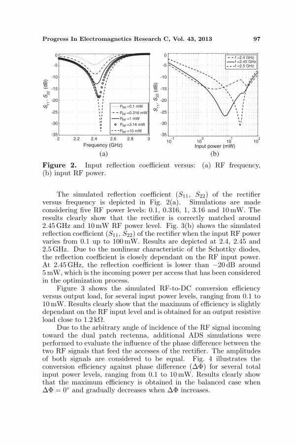
Figure 2. Input reflection coefficient versus: (a) RF frequency,(b) input RF power.
The simulated reflection coefficient (S11, S22) of the rectifierversus frequency is depicted in Fig. 2(a). Simulations are madeconsidering five RF power levels: 0.1, 0.316, 1, 3.16 and 10 mW. Theresults clearly show that the rectifier is correctly matched around2.45GHz and 10 mW RF power level. Fig. 3(b) shows the simulatedreflection coefficient (S11, S22) of the rectifier when the input RF powervaries from 0.1 up to 100mW. Results are depicted at 2.4, 2.45 and2.5GHz. Due to the nonlinear characteristic of the Schottky diodes,the reflection coefficient is closely dependant on the RF input power.At 2.45GHz, the reflection coefficient is lower than −20 dB around5mW, which is the incoming power per access that has been consideredin the optimization process.
Figure 3 shows the simulated RF-to-DC conversion efficiencyversus output load, for several input power levels, ranging from 0.1 to10mW. Results clearly show that the maximum of efficiency is slightlydependant on the RF input level and is obtained for an output resistiveload close to 1.2 kΩ.
Due to the arbitrary angle of incidence of the RF signal incomingtoward the dual patch rectenna, additional ADS simulations wereperformed to evaluate the influence of the phase difference between thetwo RF signals that feed the accesses of the rectifier. The amplitudesof both signals are considered to be equal. Fig. 4 illustrates theconversion efficiency against phase difference (∆Φ) for several totalinput power levels, ranging from 0.1 to 10 mW. Results clearly showthat the maximum efficiency is obtained in the balanced case when∆Φ = 0 and gradually decreases when ∆Φ increases.

98 Takhedmit et al.
Output load (kΩ)0 2 4 6 8 10
Effi
cien
cy (
%)
80
70
60
50
40
30
20
10
0
P =0.1 mWRF
P =0.316 mW
P =1 mWP =3.16 mW
P =10 mW
RF
RF
RF
RF
Figure 3. Conversion efficiencyversus output load.
0 20 40 60 80 100 120 140 160 180
∆Φ ( )O
80
70
60
50
40
30
20
0
Effi
cien
cy (
%)
10
P =0.1 mWRF
P =0.316 mWP =1 mWP =3.16 mWP =10 mW
RF
RF
RF
RF
Figure 4. Conversion efficiencyversus phase difference betweenthe two accesses of the rectifier.
3. RECTINNA CIRCUIT: 3D-FDTD MODELING
The rectifier previously described has been associated with two linearlypolarized patch antennas (see Fig. 5). The rectenna was etched on theRogers Duroid 5880 substrate with εr = 2.2 and 1.575 mm thickness.
The single patch antenna has been designed and optimized underAnsys HFSS software. Its dimensions are depicted on Fig. 5. The twopatches have then been arranged to form the antenna array (see Fig. 6).The radiating elements are connected through a planar tee junctionrespectively constituted by a 50Ω and 25 Ω characteristic impedancemicrostrip lines. The 50-Ω feeding lines are 6.85mm shifted at theedge of the antenna to excite the transverse vertical mode (along xcoordinate) of the antenna. This configuration is also called the H-
o y
x
Patch antenna 2
P
R
(SOT 23 package)
(SOT 23 package)
L = 48.46
Patch antenna 1
L =
24.
17
L =
39.
35
L
f
HSMS 2863
HSMS 2864
Figure 5. Layout of the proposed rectenna (All dimensions are inmillimeters).

Progress In Electromagnetics Research C, Vol. 43, 2013 99
Elevation angle ( )
Rad
iatio
n pa
ttern
-100 -50 0 50O
100
1
0.9
0.8
0.7
0.6
0.5
0.4
0.3
0.2
0.1
0
H-plane
E-plane
E-planeH-plane
Figure 6. Normalized radiation pattern of the antenna array.
plane arrangement [21]. Here, the edge-to-edge separation is 56.9 mm(λ0/2.15), resulting in a mutual coupling between patches less than−32 dB.
The array presents a simulated reflection coefficient (S11) of−22 dB. The simulated gain of the single patch antenna is 7.14 dBat 2.45 GHz at its broadside (θ = 0). This corresponds to aneffective aperture of 61.8 cm2 (123.6 cm2 for the corresponding dualpatch array). The normalized radiation pattern of the antenna arrayin the E- and H-planes is shown in Fig. 6. Two side lobes appear atθ ≈ ±60, in the H-plane.
To accurately analyze and take into account the electromagneticcouplings between the rectifying circuit and the patch antennas, thefull-wave three-dimensional Finite Difference Time Domain 3D-FDTDmethod [22] has been introduced. The algorithm has been extended tolumped linear and non-linear elements [23–26] to describe and analyzethe rectenna in term of current distributions [27]. Furthermore, thetotal-field/scattered-field formulation [28] and the Uniaxial PerfectlyMatched Layers (UPML) [29] have also been used.
The FDTD parameters will be specified and simulation resultspresented and discussed. The smallest cells in the x and y directionsare ∆x = 0.467mm and ∆y = 0.279 mm. Two cells have been chosento correctly model the substrate thickness (∆z = 0.7875 mm) alongthe z axis. The total mesh dimensions are 227 × 137 × 49 cells inthe x, y and z directions, respectively. The time step is 0.726 psand simulations are performed considering 100000 time steps. Thepatch antennas are modeled by 41 cells in length (L6) and 56 cellsin width (L5). The feed-line width W1 and length L1 are 15∆xand 11∆y, respectively. Schottky diodes (D1 to D4) are modeled by

100 Takhedmit et al.
a 0.84mm × 0.82mm × 0.7875mm cells and the output load RL isconsidered over two cells of 0.5 mm in length and one cell of 0.896 mm inwidth. Using the total-field/scattered-field formulation, the rectenna isilluminated by a linearly polarized incident plane wave of E = 19 V/m(ρ = 96µW/cm2) at its broadside.
The rectifying circuit, described in Section 2, and the patchantenna are correctly matched. They present an input impedance closeto 50Ω at 2.45GHz. Due to the absence of the input HF filters, theinfluence of the antennas on the rectifier at 4.9 and 7.35 GHz harmonicfrequencies must be evaluated in term of input impedance. Table 2shows the HFSS-simulated input impedance (real and imaginary parts)of the patch antenna at the 2.45GHz fundamental frequency and firstharmonics, computed at the feed-point Pf (see Fig. 5).
Table 2. Input impedance of the single patch antenna.
FrequencyFundamental(2.45GHz)
2nd harmonic(4.9GHz)
3rd harmonic(7.35GHz)
Rin (Ω) 48.9 16 16Xin (Ω) 5.2 −14 30.9
The matching (or mismatching) stage is obtained by accuratelyadjust the length L1 of the printed line between the antenna andthe rectifier parts. Then, a parametric study has been conducted tofind the optimal value of L1 that provides an impedance matching at2.45GHz and a mismatching at the second and third order harmonics.
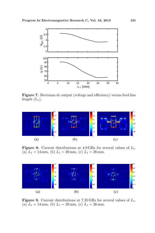
Figure 7 shows the simulated output dc voltage and efficiencywhen L1 varies from 6 up to 30 mm. The FDTD results show that theefficiency decreases from 90.8% to 57.8% and the output dc voltagevaries between 3.6 and 2.87V. For L1 = 8 mm, an output dc voltageof 3.59 V and 90.6% efficiency were obtained. When L1 decreasesfrom 8 mm to 6 mm, the rectenna output doesn’t change greatly(VDC = 3.6V and η = 90.8%). Therefore, this line length was setto be 8 mm for the experimental realization.
To accurately evaluate the influence of the line-length L1 on therectifier behavior at both second and third order harmonics, FDTDcurrent distributions on transmission lines have been calculated forthree different values of L1 (14, 20 and 26 mm), after Fast FourierTransform (FFT) computation. The current distributions (Js) arecomputed using tangential components of magnetic field (Hx and Hy).Results are depicted in Figs. 8 and 9.
When L1 varies, the amount of power generated by the diodes at4.9 and 7.35 GHz could be transmitted to antennas where superficial
Progress In Electromagnetics Research C, Vol. 43, 2013 101
4
3.5
3
2.5
2
V
(V
)D
C
100
90
80
70
60
50
η (
%)
0 5 10 15 20 25 30 35
L (mm)1
Figure 7. Rectenna dc output (voltage and efficiency) versus feed-linelength (L1).
(a) (b) (c)
Figure 8. Current distributions at 4.9 GHz for several values of L1.(a) L1 = 14 mm, (b) L1 = 20 mm, (c) L1 = 26 mm.
(a) (c)(b)
Figure 9. Current distributions at 7.35GHz for several values of L1.(a) L1 = 14 mm, (b) L1 = 20 mm, (c) L1 = 26 mm.

102 Takhedmit et al.
current appears on the patches (L1 = 26 mm) and then radiated. Thereis no input lowpass filter and then, the patch antenna acts as a load forthe rectifier at high order harmonics. This may modify the behaviorof the rectifier and can decrease its performances.
Figure 10 shows the current distributions on transmission linescomputed in the frequency domain when L1 is optimal and set to be8mm. This study will be limited to the 7.35 GHz third order harmonic.Results show that all diodes (D1 to D4) have the same dc current andthat flowing through the output load RL is twice.
(a) (b)
(c) (d)
Figure 10. Current distributions Js (A/m). (a) DC, (b) 2.45 GHz,(c) 4.9 GHz, (d) 7.35GHz.
At 2.45 GHz, two folded quarter wavelength open stubs, connectedto points P9 and P10, behave like short circuits (a peak of currentappears on the main lines). These stubs block the unwanted 2.45GHzfundamental frequency and isolate the resistive load RL.
At the 4.9 GHz second harmonic, the Schottky diodes have beenaccurately localized on a null of the current to minimize the powerlosses. In addition, the distance between D1 (D3) and D2 (D4) isthree times half-wavelength at 4.9 GHz. Consequently, the secondorder harmonic is then distributed by a standing wave inside the mainclosed loop P1-P2-P1 with a peak of current (∼ short circuit) at pointsP1 and P2. The unwanted second harmonic has been confined andthere are no propagation effects towards microstrip patch antennas,

Progress In Electromagnetics Research C, Vol. 43, 2013 103
where no current exists.The results clearly show that the 7.35 GHz third-order harmonic
has a very low level and is reduced. It is mainly confined anddistributed by a standing wave inside the rectifier part between pointsP7 and P8. By finely adjust the feed-line length (L1 = 8 mm), theantenna and the rectifier have been mismatched at this harmonic. Thecurrent distribution also shows that there are no propagation effectstowards antennas, where no current appears.
4. EXPERIMENTAL CHARACTERIZATION
The rectenna shown in Fig. 5 has been realized and experimentallycharacterized inside an anechoic chamber using the dedicatedmeasurement setup shown in Fig. 11. It contains an RF generator(Agilent E8251A) and a transmitting horn antenna (Gt = 12 dB). Inaddition, a power amplifier with 37 dB gain has been connected to theRF source to increase the transmitted power. The rectenna is localizedin the far field zone ((2.D2/λ0) > 53 cm) at a distance of d = 1m fromthe transmitter. The output dc voltage across RL has been measuredby a voltmeter.
Anechoic chamber
Power
Amplifier
RF
generator
Horn
antenna
d = 1 mRectenna
circuit
Voltmeter
Figure 11. Dedicated measurement setup.
Two dedicated measurements have been performed. The first oneconsists to measure the dc voltage and efficiency as a function of powerdensity and the second one consists to measure the output voltage asa function of elevation angle (θ) in both E- and H-planes (Φ = 0 and90).
The overall efficiency (η) of the rectenna is defined as the ratiobetween the output dc power and the effective RF power. The Friistransmission equation including effective aperture of antennas andcable losses gives this effective incident RF power (PRF) toward therectifier [13].

104 Takhedmit et al.
The single patch antenna has been realized and experimentallycharacterized. It has a maximum gain of 6.2 dB and an effectiveaperture of 49.8 cm2. Thus, the total effective aperture of the dualpatch array is set to be twice (99.6 cm2). The differences withthe simulated results are mainly due to the tolerances during thefabrication process but also to the errors during the measurements.
The measured and FDTD simulated output dc voltages whenreceived power density varies from 0 to 158µW/cm2 (E = 24.4V/m,PRF = 15.7mW), are shown in Fig. 12(a). Experimental and FDTDcurves are similar and are very close. The dc voltage increases whenpower density increases. For a low power density of 4.5µW/cm2
(E = 4.1 V/m, PRF = 0.45mW), an output voltage of 0.5 V wasmeasured across an optimal load of 1.2 kΩ. A maximum voltage of4V was measured when the power density is 158µW/cm2. Fig. 12(b)compares the measured and FDTD simulated rectenna efficiencies asa function of power density (0–158µW/cm2).
(a) (b)
0
0.5
1
1.5
2
2.5
3
3.5
4
4.5
Outp
ut voltage (
V)
FDTD method Measured
0 0.02 0.04 0.06 0.08 0.1 0.12 0.14 0.16 0.18
0
10
20
30
40
50
60
70
80
90
100
Power density (mW/cm )
Recte
nna e
ffic
iency (
%)
FDTD methodMeasured
2
0 0.02 0.04 0.06 0.08 0.1 0.12 0.14 0.16 0.18
Power density (mW/cm )2
Figure 12. Simulated and measured (a) dc output voltage,(b) efficiency versus power density.
The experimental efficiency has a minimum value of 51.1% andis obtained at 4.5µW/cm2. It exceeds 72% from 14µW/cm2 (E =7.3V/m, PRF = 1.4 mW) and is above 80% from 43µW/cm2 (E =12.8 V/m, PRF = 4.3mW). Measurements are in good agreement withsimulations. The differences between experiments and FDTD resultsare less than 3% in the power density range of 0–158µW/cm2.
Figure 13 shows a comparison between measured and FDTDsimulated output voltage as a function of elevation angle (θ) in bothE- and H-planes. To compare experimental and FDTD results, therectenna was illuminated so that it receives the same RF power in bothcases. In FDTD simulations, an incident plane wave of 96µW/cm2
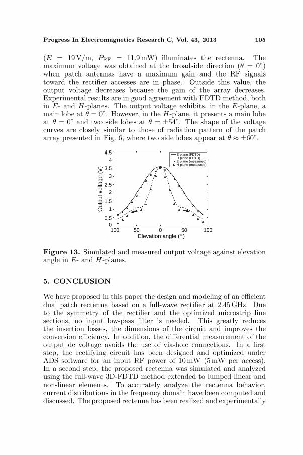
Progress In Electromagnetics Research C, Vol. 43, 2013 105
(E = 19 V/m, PRF = 11.9mW) illuminates the rectenna. Themaximum voltage was obtained at the broadside direction (θ = 0)when patch antennas have a maximum gain and the RF signalstoward the rectifier accesses are in phase. Outside this value, theoutput voltage decreases because the gain of the array decreases.Experimental results are in good agreement with FDTD method, bothin E- and H-planes. The output voltage exhibits, in the E-plane, amain lobe at θ = 0. However, in the H-plane, it presents a main lobeat θ = 0 and two side lobes at θ = ±54. The shape of the voltagecurves are closely similar to those of radiation pattern of the patcharray presented in Fig. 6, where two side lobes appear at θ ≈ ±60.
100 50 0 50 1000
0.5
1
1.5
22.5
3
3.5
44.5
Elevation angle ( )
Out
put v
olta
ge (
V)
E plane (FDTD)H plane (FDTD)E plane (measured)H plane (measured)
o
Figure 13. Simulated and measured output voltage against elevationangle in E- and H-planes.
5. CONCLUSION
We have proposed in this paper the design and modeling of an efficientdual patch rectenna based on a full-wave rectifier at 2.45GHz. Dueto the symmetry of the rectifier and the optimized microstrip linesections, no input low-pass filter is needed. This greatly reducesthe insertion losses, the dimensions of the circuit and improves theconversion efficiency. In addition, the differential measurement of theoutput dc voltage avoids the use of via-hole connections. In a firststep, the rectifying circuit has been designed and optimized underADS software for an input RF power of 10 mW (5 mW per access).In a second step, the proposed rectenna was simulated and analyzedusing the full-wave 3D-FDTD method extended to lumped linear andnon-linear elements. To accurately analyze the rectenna behavior,current distributions in the frequency domain have been computed anddiscussed. The proposed rectenna has been realized and experimentally

106 Takhedmit et al.
characterized. It exhibits a measured efficiency of 73% at a powerdensity of 14µW/cm2 (E = 7.3 V/m, PRF = 1.4mW) and 84% at43µW/cm2 (E = 12.8V/m, PRF = 4.3mW). An output dc voltageof 4 V has been measured through an optimal load of 1.2 kΩ when thepower density is 158µW/cm2. Measured results are very close to thoseobtained by the full-wave 3D-FDTD simulations. The differences onthe efficiency are less than 3% over the power density range from 0to 158µW/cm2. The reported circuit can be useful for wireless powertransmission applications. It should also find applications in ambientelectromagnetic energy recycling, where power densities are relativelylow. This new rectenna is particularly suitable to power remote supplyof wireless and low consumption sensors, sensor nodes and actuators.
ACKNOWLEDGMENT
This work is supported by the ANR (Agence Nationale de la Recherche)through the project REC-EM ANR-10-BLAN-0906.
REFERENCES
1. Brown, W. C., “The history of power transmission by radiowaves,” IEEE Trans. Microw. Theory and Tech., Vol. 32, No. 9,1230–1242, Sep. 1984.
2. Ren, Y. J. and K. Chang, “5.8-GHz circularly polarized dual-dioderectenna and rectenna array for microwave power transmission,”IEEE Trans. Microw. Theory and Tech., Vol. 54, No. 4, 1495–1502, Apr. 2006.
3. Douyere, A., J. D. Lan, S. Luk, and F. Alicalapa, “High efficiencymicrowave rectenna circuit: Modeling and design,” ElectronicsLetters, Vol. 44, No. 24, Nov. 2008.
4. Zbitou, J., M. Latrach, and S. Toutain, “Hybrid rectenna andmonolithic integrated zero-bias microwave rectifier,” IEEE Trans.Microw. Theory and Tech., Vol. 54, No. 1, 147–152, Jan. 2006.
5. Strassner, B. and K. Chang, “5.8-GHz circularly polarizedrectifying antenna for wireless microwave power transmission,”IEEE Trans. Microw. Theory and Tech., Vol. 50, No. 8, 1870–1876, Aug. 2002.
6. Heikkinen, J. and M. Kivikoski, “Low-profile circularly polarizedrectifying antenna for wireless power transmission at 5.8 GHz,”IEEE Microw. Wireless Compon. Lett., Vol. 14, No. 4, 162–164,Apr. 2004.

Progress In Electromagnetics Research C, Vol. 43, 2013 107
7. Heikkinen, J. and M. Kivikoski, “A novel dual-frequency circularlypolarized rectenna,” IEEE Antennas Wireless Propag. Lett.,Vol. 2, 330–333, 2003.
8. Akkermans, J. A. G., M. C. van Beurden, G. J. N. Doodeman, andH. J. Visser, “Analytical models for low-power rectenna design,”IEEE Antennas Wireless Propag. Lett., Vol. 4, 187–190, 2005.
9. Takhedmit, H., B. Merabet, L. Cirio, B. Allard, F. Costa,C. Vollaire, and O. Picon, “Design of a 2.45GHz rectennausing a global analysis technique,” Proceed. of the 3rd EuropeanConference on Antennas and Propagation, EuCAP 2009, 2321–2325, Berlin, Germany, Mar. 23–27, 2009.
10. Marian, V., C. Vollaire, J. Verdier, and B. Allard, “An alternativeenergy source for low power autonomous sensors,” Proceed. of the5th European Conference on Antennas and Propagation, EuCAP2011, 405–409, Rome, Italy, Apr. 11–15, 2011.
11. Ahn, C.-H., S.-W. Oh, and K. Chang, “A high gain rectifyingantenna combined with reflectarray for 8 GHz wireless powertransmission,” IEEE International Symposium on Antennas andPropagation, APSURSI 2009, 1–4, Charleston, USA, Jun. 1–5,2009.
12. Olgun, U., C.-C. Chen, and J. L. Volakis, “Investigationof rectenna array configurations for enhanced RF powerinvestigation,” IEEE Antennas Wireless Propag. Lett., Vol. 10,262–265, 2011.
13. Epp, L. W., A. R. Khan, H. K. Smith, and R. P. Smith, “Acompact dual-polarized 8.51-GHz rectenna for high-voltage (50 V)actuator applications,” IEEE Trans. Microw. Theory and Tech.,Vol. 48, No. 1, 111–119, Jan. 2000.
14. Takhedmit, H., L. Cirio, B. Merabet, B. Allard, F. Costa,C. Vollaire, and O. Picon, “A 2.45-GHz dual-diode rectenna andrectenna arrays for wireless remote supply applications,” Intern.Journ. of Microw. and Wireless Technolog., Vol. 3, Special issue 3,251–258, Jun. 2011.
15. Monti, G., L. Corchia, and L. Tarricone, “ISM band rectennausing a ring loaded monopole,” Progress In ElectromagneticsResearch C, Vol. 33, 1–15, 2012.
16. Monti, G. and F. Congedo, “UHF rectenna using a bowtieantenna,” Progress In Electromagnetics Research C, Vol. 26, 181–192, 2012.
17. Falkenstein, E., M. Roberg, and Z. Popovic, “Low-power wirelesspower delivery,” IEEE Trans. Microw. Theory and Tech., Vol. 60,No. 7, 2277–2286, Jul. 2012.

108 Takhedmit et al.
18. Farinholt, K. M., G. Park, and C. R. Farrar, “RF energytransmission for low-power wireless impedance sensor node,”IEEE Sensors Journal, Vol. 9, No. 7, 793–800, Jul. 2009.
19. Advanced Design System software, Agilent Technologies, 2000–2013, Available: http://www.home.agilent.com/.
20. HSMS-286x, HSMS-282x series, Surface Mount Mi-crowave Schottky Detector Diodes, 2001, Avail-able: http://www.avagotech.com/.
21. Balanis, C. A., Antenna Theory: Analysis and Design, 3rdEdition, John Wiley & Sons, Inc., 2005.
22. Taflove, A. and S. C. Hagness, “Computational electrodynamics— The finite difference time domain method,” 3rd Edition, ArtechHouse Inc., 2005.
23. Sui, W., D. A. Christensen, and C. H. Durney, “Extending the twodimensional FD-TD method to hybrid electromagnetic systemswith active and passive lumped elements,” IEEE Trans. Microw.Theory and Tech., Vol. 40, 724–730, 1992.
24. Toland, B., B. Houshmand, and T. Itoh, “FDTD analysis ofan active antenna,” IEEE Microwave and Guided Wave Letters,Vol. 3, No. 11, 423–425, Nov. 1993.
25. Kuo, C.-N., R.-B. Wu, B. Houshmand, and T. Itoh, “Modelingof microwave active devices using the fdtd analysis based onthe voltage-source approach,” IEEE Microwave and Guided WaveLetters, Vol. 6, No. 5, 199–201, May 1996.
26. Kuo, C.-N., B. Houshmand, and T. Itoh, “Full-wave analysis okpackaged microwave circuits with active and nonlinear devices:an FDTD approach,” IEEE Trans. Microw. Theory and Tech.,Vol. 45, No. 5, 819–826, May 1997.
27. Takhedmit, H., L. Cirio, B. Merabet, B. Allard, F. Costa,C. Vollaire, and O. Picon, “Efficient 2.45 GHz rectenna designincluding harmonic rejecting rectifier device,” Electronics Letters,Vol. 46, No. 12, 811–812, Jun. 10th, 2010.
28. Umashankar, K. and A. Taflove, “A novel method to analyzeelectromagnetic scattering of complex objects,” IEEE Trans. onElectromagnetic Compatibility, Vol. 24, No. 4, 397–405, Nov. 1982.
29. Gedney, S. D., “An anisotropic perfectly matched layer-absorbingmedium for the truncation of FDTD lattices,” IEEE Trans.Antennas and Propagation, Vol. 44, No. 12, 1630–1639, Dec. 1996.