Embed Size (px)
Citation preview
Design and Control of a MEMS Nanopositioner with BulkPiezoresistive Sensors
Mohammad Maroufi, Y. K. Yong1 and S. O. Reza Moheimani2
Abstract— A 2 degree of freedom microelectromechanicalsystem (MEMS) nanopositioner is presented in this paper.The nanopositioner is fabricated using a standard silicon-on-insulator process. The device demonstrates a bidirectionaldisplacement in two orthogonal directions. As the displacementsensing mechanism, bulk piezoresistivity of tilted clamped-guided beams is exploited. The characterization reveals morethan 15 μm displacement range and an in-plane bandwidthof above 3.6 kHz in both axes. The piezoresistive sensorsprovide a bandwidth which is more than ten times largerthan the stage’s resonant frequency. To evaluate the sensorperformance in closed-loop, an integral resonant controllertogether with an integral tracking controller are implementedwhere piezoresistive sensor outputs are used as measurement.The controlled nanopositioner is used for imaging in an atomicforce microscope.
I. INTRODUCTION
The invaluable feature of nanopositioners for producing
displacements with nanometer and sub-nanometer resolution
made these devices a crucial instrument for numerous state-
of-the-art applications. Nanolithography [1], scanning probe
microscopy [2] and probe data storage systems with ultrahigh
density [3] are among the example of such applications.
Recently, the microelectromechanical system (MEMS)
nanopositioners have also found applications as scanners in
on-chip atomic force microscopes (AFM) [4] and probe data
storage systems [5].
For realization of MEMS nanopositioner, a range of actu-
ation and sensing mechanisms can be used. As actuators,
electrostatic and electrothermal actuation mechanisms are
more prevalent. In comparison with electrostatic actuators,
electrothermal actuators provide a relatively high force. How-
ever, their sluggish dynamics, due to the involvement of heat
transfer mechanism, limits their use in high-speed MEMS
nanopositioners.
Displacement sensing mechanisms such as capacitive [6],
electrothermal [7] and piezoresistive [8] can be incorporated
in MEMS devices. The capacitive sensing mechanism, in
particular, is predominately used in MEMS nanopositioners
(for example see [9]–[11]). The implementation of capacitive
sensors is often compatible with standard microfabrication
processes and they typically demonstrate a high-resolution
*This work is supported by Australian research council (ARC).1Mohammad Maroufi and Y. K. Yong are with the School of
Electrical Engineering and Computer Science, University of Newcas-tle, Callaghan, NSW 2308, Australia, [email protected],[email protected]
2S. O. Reza Moheimani was with the School of Electrical Engineeringand Computer Science, University of Newcastle, Australia. He is now withthe Department of Mechanical Engineering, the University of Texas atDallas, Richardson, TX 75080, USA, [email protected]
performance in a wide bandwidth. However, using this
sensing mechanism typically necessitates the allocation of a
part of nanopositioners’ mechanical structure to the sensing
capacitors, which leads to an occupation of an extra area of
the chip. In addition, a relatively complex readout circuit is
needed to detect small capacitance changes at the presence
of parasitic capacitors [12].
The electrothermal sensors typically comprise a pair of
heaters and a stage which functions as a heat sink. The
displacement is measured based on the temperature varia-
tions and, as a result, opposite resistance changes in the
pair of heaters induced by the stage displacement [13],
[14]. Small form factor and the requirement of a relatively
simple readout circuit are among the benefits of utilizing
this sensor. Electrothermal sensors are also implemented
in MEMS nanopositioners [4], [15]. However, their limited
bandwidth poses a restriction on the achievable scanning
speed of the MEMS nanopositioner.
Piezoresistivity of silicon, which is the variation of its
electrical conductivity under mechanical stress, has also been
exploited as sensing mechanism in MEMS nanopositioners
[8], [16]. These displacement sensors are normally realized
by implementing heavily doped areas on high-stressed zones
of silicon flexures. These sensors require relatively simple
readout circuitry and, in contrast to the electrothermal sen-
sors, offer a wide sensing bandwidth. The implementation
of the piezoresistive sensors, however, requires additional
and often non-standard fabrication steps which hinders their
widespread application.
To address the implementation problem, we proposed
a novel piezoresistive displacement sensor in [17], which
excluded the need for additional fabrication and doping steps.
In that design, the bulk piezoresistivity of entire structure of
a pair of tilted beams was exploited rather than some heavily
doped small zones. In addition, the mechanical structure was
designed such that the sensors operates differentially.
In this paper, a 2-DOF MEMS nanopositioner with the
tilted beam piezoresistors is proposed to be incorporated as
a scanner within an AFM. The titled beams also function
as a part of the device’s suspension system, so the space
allocated to this sensing mechanism is practically zero. For
the implementation, the standard SOIMUMPs process is used
[18]. The characterization reveals a relatively large displace-
ment range and mechanical bandwidth. By a proper design,
the bandwidth of displacement sensors is also enhanced.
Thus, the senors completely capture the device dynamics
in a frequency range which is ten times larger than the
first mechanical resonant mode. The static and dynamic
2015 IEEE Conference on Control Applications (CCA)Part of 2015 IEEE Multi-Conference on Systems and ControlSeptember 21-23, 2015. Sydney, Australia
978-1-4799-7787-1/15/$31.00 ©2015 IEEE 1455

Fig. 1: The SEM image of the MEMS nanopositioner. The
close-up views show folded springs and tethering beams, the
electrostatic actuators, gold features and the piezoresistive
sensor in the Y direction.
TABLE I: The geometrical properties of the proposed MEMS
nanopositioner.
Tilted-beam Normal Length: h = 1mm Width:10 μmsensors Inclination distance, angle: Δ = 15 μm, δ = 0.86◦
Comb fingerAir gap: 2 μm Engagement:12μmLength: 26 μm Width:2 μm
Comb structures Trapezoidal: Length:1536μm, Bases: 20 μm,75 μm
Shuttle beams 2443 μm×250 μm
Tethering beams 500 μm×5 μm, 8 on each side
characterizations of the nanopositioner show that outputs of
the piezoresistive sensors are deemed suitable to be used
as measurement in a feedback control loop. An integral
resonant controller (IRC) combined with an integral tracking
controller are implemented in closed-loop to evaluate the
performance of the proposed MEMS nanopositioner in the
raster scan [19]. Finally, the controlled nanopositioner is used
as a scanner table within a commercially available AFM.
II. NANOPOSITIONER’S DESIGN AND FABRICATION
The scanning electron microscope (SEM) image of the
proposed nanopositioner is shown in Fig. 1. A stage with
the dimension of 1.8mm× 1.8mm is located at the center
of the nanopositioner, functioning as the scan table. The
nanopositioner has a parallel-kinematic configuration where
it is capable of moving bidirectionally along X and Y axes.
The device is realized using the standard SOIMUMPs micro
δ
h
Rp1
Rp2
v
Vqva
Vqva
viR1
R2
Rp1
Rp2
A
bV
Fig. 2: a) Schematic of the piezoresistive sensor structure
when the shuttle beam moves to the right. For the sake
of clarity, the deflected shapes of the folded beam springs
are not shown. b) The sensing circuit based on Wheatstone
bridge. c) Schematic of the actuation circuit.
fabrication process [18]. The process is a silicon-on-insulator
MEMS fabrication method with 25 μm thick single crystal
silicon as the device layer. As shown in Fig. 1, square-shaped
gold features with the size of 4 μm×4 μm are also fabricated
on the stage to be used as sample patterns for AFM imaging.
Electrostatic comb-drive actuators are implemented on
each side of the stage to provide the necessary force. As
shown in Fig. 1, the mass of the comb structures is reduced
by using of trapezoidal geometry.
To transfer the actuation force to the stage, a shuttle beam
is utilized on each side. Tethering beams connect the shuttle
beams to the stage, while their lateral compliance allows
the stage to move in two orthogonal directions. As part of
the mechanical suspension system, eight folded springs are
implemented on each side. Each spring comprises two pairs
of parallel beams connected to a relatively thick beam in
the middle. These folded springs are incorporated instead of
the typical clamped-guided beams to achieve a more linear
stiffness-displacement behavior [20]. Geometrical properties
of the nanopositioner is summarized in Table I.
As clear in Fig. 1, two pairs of tilted beams in a V-
shaped configuration are implemented for all shuttle beams
functioning as a part of device’s suspension system. The
close-up view in this figure also shows that the piezoresistive
1456
sensor in each direction comprises two pairs of these tilted
beams. The structural configuration of the displacement
sensor is further illustrated in Fig. 2a. A pair of the tilted
beams is gold plated which constructs a short-circuited path
to the electrical ground, while the piezoresistivity of the other
pair is used for displacement sensing. Due to the tilted geom-
etry, the displacement of the shuttle beam induces an axial
tensile force in one tilted beam and an axial compressive
force along the other. These longitudinal forces cause their
resistance (Rp1 and Rp2) to change in opposite directions due
to the inherent piezoresistivity of silicon [17]. As clear in
Fig. 2b, the resistance variations are subsequently converted
to a voltage using a Wheatstone bridge and differentially
amplified by an instrumentation amplifier at the output.In [17], this piezoresistive sensor was implemented for a 1-
DOF MEMS nanopositioner, where a large feedthrough sig-
nal from actuation to sensing was observed. That feedthrough
signal limited the sensor’s bandwidth to about 8kHz [21].
In the nanopositioner presented here, however, the on-chip
signal routing is modified to alleviate the feedthrough signal
in the piezoresistive sensors, which dramatically increases
their sensing bandwidth.
III. CHARACTERIZATION
For all experiments, the linear actuation mechanism is
implemented for the device in both directions [22]. The
actuation circuit is schematically shown in Fig. 2c for one
axis, where the actuation voltage designated as va with
opposite sign plus a constant dc voltage (Vq) are applied to
the electrostatic combs. The stage and the moving combs
are connected to the electrical ground. Here, the stage
experiences a net actuating force which depends linearly on
the (Vq×va). A 45V dc bias voltage (Vq in Fig. 2c) is applied
during all tests.The bias voltage for the sensor in both direction (Vb in
Fig. 2b) is adjusted to 6V. In the absence of the actuation
voltage, when the stage is at its equilibrium position, the
outputs of the sensors are adjusted to zero using the poten-
tiometers in their readout circuits.
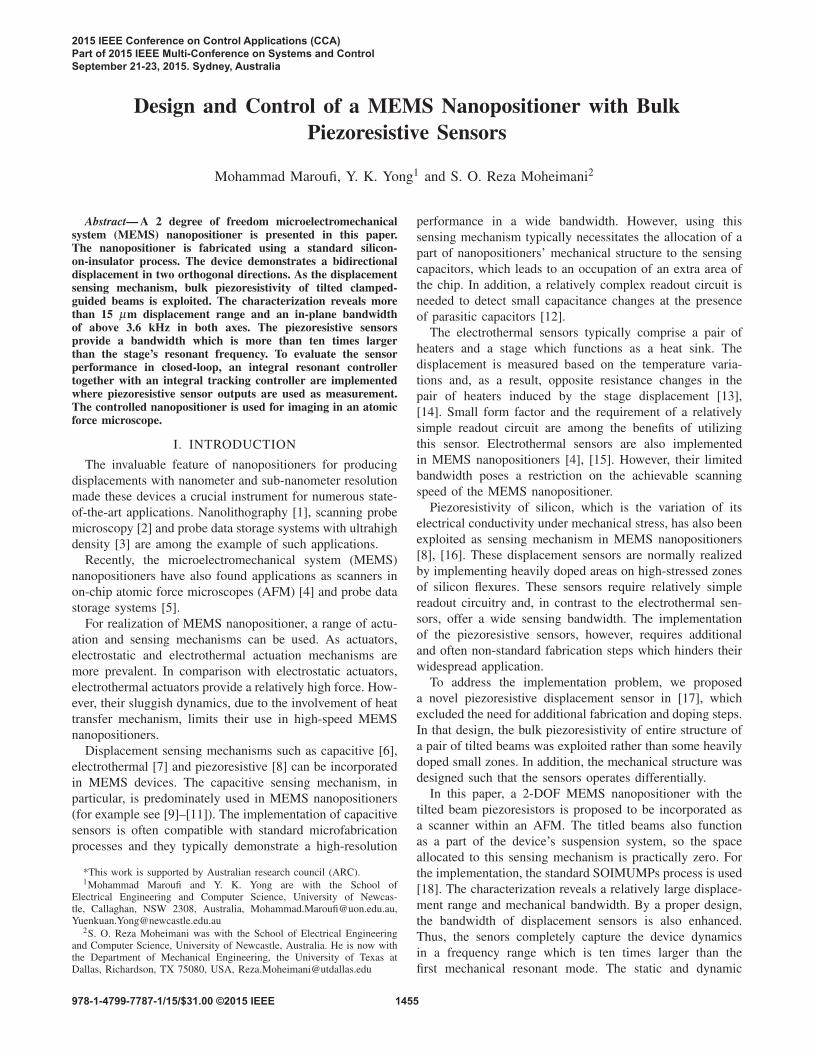
A. Static ResponseThe stage displacement is experimentally measured in both
X and Y axes using Polytec MSA-050-3D Micro System
Analyzer (MSA). Fig. 3 plots the X and Y displacement
of the stage as a function of the actuation voltage (va). A
linear actuation-displacement behavior is observed, where a
displacement range of 16 μm and 15 μm are obtained in the
X and Y directions, respectively.The piezoresistive sensors output is also recorded simul-
taneously and presented in Fig. 3. A linear relationship
between sensor outputs and the stage displacement is ob-
servable and calibration factors of 0.208 V/μm and 0.220 V/μm
are obtained for the piezoresistive sensors in X and Y axes,
respectively.A negligible cross coupling (approximately −40dB) is
also measured between the two perpendicular axes, which is
sufficient to consider the system as two single-input single-
output (SISO) systems.
−30 −20 −10 0 10 20 30−10
−5
0
5
10
Dis
plac
emen
t (μm
)
Actuation Voltage (V)
−2
−1
0
1
2
Sen
sor
Out
put(
V)
X Displacement
Y Displacement
X Sensor
Y Sensor
Y Sensor
X Sensor
X Displ.
Y Displ.
Fig. 3: The displacement of the stage and the piezoressitive
sensors output are presented versus actuation voltage (va) for
both directions.
B. Dynamic Response
The frequency response of the nanopositioner is also ob-
tained by applying a chirp signal with a bandwidth of 40kHz
as va in order to excite the system. The displacement of the
stage is directly recorded using the MSA. The frequency
responses of the device along the X and Y axes are shown
in Fig. 4. The first in-plane frequency occurs at 3626Hz and
3944Hz for the X and Y axes, respectively.
In Fig. 4 the frequency responses of the sensors output are
also compared with the system displacement in both axes.
For the sake of clarity, the dc gain of the responses are
adjusted to unity. As visible, the sensors completely capture
the dynamics of the system in a frequency range more than
ten times larger than the first mechanical resonant mode in
both axes.
The noise at the sensors output is recorded in the time
domain sampled at 128 kHz for all sensors within a time
duration of 25 s. The resolution of the sensor is 2nm and
1.9nm in the X and Y axes, respectively. The resolution of
the sensor is defined as the root mean square (RMS) value
of the noise signals which are converted to a displacement
resolution using the calibration factors.
The device demonstrates a relatively high-bandwidth with
a displacement range more than 15 μm in both axes. In
addition, the piezoresistive displacement sensors entirely
capture the systems dynamic in a large frequency range
without inducing any delay or phase lag. This makes the
device favorable for the implementation of various control
algorithms. An integral resonant controller (IRC) plus an
integral tracking controller are implemented for the device
as explained next.
IV. CONTROLLER IMPLEMENTATION
The performance of the MEMS nanopositioner is eval-
uated in closed-loop. In order to design a controller, the
transfer function of the open-loop plant, from the actuation
signal to the sensor output, is initially identified using the
least square method [23] as:
Gx =−6.543×10⁻⁶s+0.9773
1.921×10⁻⁹s2 +9.101×10⁻⁷s+1, (1)
1457

102
103
104
−40
−20
0
20
40
Mag
nitu
de (
dB)
102
103
104−300
−200
−100
0
Pha
se (
deg.
)
Frequency (Hz)
Displacement
Sensor Output
Identified Model
Identified Model
(a) X axis
102
103
104
−40
−20
0
20
40
Mag
nitu
de (
dB)
102
103
104−300
−200
−100
0
Pha
se (
deg.
)
Frequency (Hz)
DisplacementSensor OutputIdentified Model
Identified Model
(b) Y axis
Fig. 4: The frequency response of the MEMS nanopositioner
in the X direction (a) and Y direction (b) obtained using
the MSA, and piezoresistive sensors in either sides. The
frequency response of the identified model (with the unity dc
gain) is also compared with the sensor output in both axes.
Gx/y++- ki
s
ref. - k
s+kD
Fig. 5: Schematic of the damping (inner) and tracking (outer)
feedback control loops of the MEMS nanopositioner.
Gy =−4.172×10⁻⁶s+0.8818
1.634×10⁻⁹s2 +9.965×10⁻⁷s+1. (2)
In Fig. 4, the frequency responses of the identified models
are compared with the sensors responses. A close agreement
is observable while each second order model (Gx/y ) captures
the first resonant mode of the nanopositioner accurately.
As shown in Fig. 5, an IRC is designed and implemented
to augment damping to each lateral axis. A high-gain integral
control is implemented in the outer feedback loop to provide
tracking.
To design IRC, a feedthrough term D is added to the
plant so that Gx/y +D has an interlacing zero-pole pattern
rather than the typical pole-zero pattern for lightly damped
Fig. 6: Measured frequency responses of the MEMS nanopo-
sitioning system for open-loop system (blue), closed-loop
damped system with IRC (green) and closed-loop system
with IRC and integral tracking control (red).
structures. The loop gain of the modified system Gx/y +Dis then analyzed in order to find the integral gain k that
provides maximum damping to the system. k is determined
using root-locus plot and the IRC is obtained as:
CIRC(s) =−k
s+ kD=
−1000
s+20000. (3)
Since the dominant resonant behavior of the X and Y axes
are almost similar, the above IRC can be implemented to
both axes. Fig. 6 shows the open- and closed-loop frequency
responses of the X axis. The Y axis has similar frequency
responses and will not be presented for brevity sake. With
the IRC loop in place, the dominant resonant peak was
suppressed by approximately 33dB. This allows a relatively
high-gain integral tracking controller to be implemented in
the outer loop with gain and phase margins of 13dB and
64.5◦, respectively. The tracking bandwidth of the closed-
loop system is 466Hz.
The step responses of the device in open-loop, in closed-
loop with IRC and both IRC and integral tracking controller
are compared in Fig. 7. The system shows an under-damped
behavior in open-loop with a settling time of approximately
12ms. The transient behavior of the system is drastically
improved with IRC and the settling time is reduced to 3.1ms.
With integral action as the second loop, the settling time is
further reduced to 1.3ms.
Fig. 8 shows the tracking performance of the closed-loop
system where the X axis was forced to follow a 25Hz
and 125Hz triangular references. The RMS tracking error
(Error 1 in Fig. 8) at 25Hz is 170nm. The error RMS
increases to 863nm at 125Hz. This is expected as the
tracking bandwidth of the closed-loop system reduces at high
frequencies, which can also be observed from the frequency
response in Fig. 6. A part of this error is simply due to a con-
stant phase lag between the reference signal and closed-loop
1458

0 2 4 6 8 10 12 14 16 18
0
0.2
0.4
0.6
0.8
1
1.2
1.4
1.6
1.8
Time (ms)
Nor
mal
ized
Out
put
(V)
ReferenceOpen LoopIRCIRC+Integral tracking
Fig. 7: The step responses of the nanopositioner in open-loop
and closed-loop with IRC and IRC plus integral tracking.
1 1.01 1.02 1.03 1.04 1.05 1.06 1.07 1.08 1.09 1.1
−6
−4
−2
0
2
4
6
Time (s)
Dis
plac
emen
t (μm
)
ReferenceSensorError1Sensor without delayError2
(a) 25Hz
8 10 12 14 16 18 20 22 24 26 28
−6
−4
−2
0
2
4
6
Time (ms)
Dis
plac
emen
t (μm
)
ReferenceSensorError1Sensor without delayError2
(b) 125Hz
Fig. 8: Tracking performance of the nanopositioner in the X
axis. A triangular reference signal with more than 12 μm
peak-to-peak displacement is applied.
system output. As visible in Fig. 6, the phase lags are 1.752◦and 8.88◦ for 25Hz and 125Hz, respectively. By shifting the
sensor signal in time domain according to these phase lags,
the RMS values of the error (Error 2 in Fig. 8) decreases
to 85nm for 25Hz and 256nm for 125Hz. The tracking
bandwidth can be improved significantly by implementing
inversion-based feedforward technique [2], [4], [24].
V. IMAGING
The proposed nanopositioner is also implemented as the
scanning stage within a commercial Nanosurf Easyscan 2
AFM. The AFM’s probe is landed on the stage and the
Fig. 9: The AFM image of the features on the stage obtained
using raster scan method with the frequency of 25Hz.
embedded in-plane nanopositioner of the probe within the
Nanosurf AFM is bypassed during the tests. The nanopo-
sitioner is operated in closed-loop and the imaging is per-
formed via constant-height contact mode. The gold features
on the stage are used as the reference pattern. In Fig. 9,
an AFM image of the gold features with 520nm height is
shown. The scan is performed in a 12 μm×12 μm window,
while a triangular signal with 25 Hz frequency is applied
to the X axis and the Y axis follows a slow ramp. The tip
deflection of the cantilever is measured using the embedded
laser sensor of the AFM. The topography of the features is
obtained using the piezoresistive sensors and the laser sensor
signals as the in-plane position and the features height data,
respectively.
VI. CONCLUSION
A 2-DOF electrostatic MEMS nanopositioner is proposed
to be used as a scanner stage in AFM. As the sens-
ing mechanism, the bulk piezoresistivity of tilted clamped-
guided beams is exploited and a standard silicon-on-insulator
microfabrication process is used for the implementation.
The characterization of the device demonstrates displacement
range and in-plane resonance modes of above 15 μm and
3.6kHz, respectively in both axes. The electrostatic combs
are actuated linearly and the sensors output shows a linear
relation with respect to the stage displacement. The sensors
entirely capture the dynamic of the stage in a bandwidth ten
times larger than the first mechanical resonance of the device.
The linear behavior of the nanopositioner plus the high-
bandwidth sensing capability of its sensors make the device
promising to be used in different control algorithms. In this
study, an IRC together with an integral tracking controller
are implemented and a bandwidth of 466Hz is obtained in
closed-loop. The tracking performance of device is tested
with a triangular reference signal with an amplitude more
than 6 μm with 25 Hz and 125Hz frequencies and finally,
by implementation of raster scan method, the device is used
as a scan table for imaging within an AFM.
REFERENCES
[1] K. Salaita, Y. Wang, and C. A. Mirkin, “Applications of dip-pennanolithography,” Nat Nano, vol. 2, no. 3, pp. 145–155, Mar. 2007.
1459

[2] S. P. Wadikhaye, Y. K. Yong, and S. O. Reza Moheimani, “A serial-kinematic nanopositioner for high-speed atomic force microscopy,”Review of Scientific Instruments, vol. 85, no. 105104, 2014.
[3] E. Eleftheriou, “Nanopositioning for storage applications,” AnnualReviews in Control, vol. 36, no. 2, pp. 244–254, Dec. 2012.
[4] M. Maroufi, A. Bazaei, and S. O. R. Moheimani, “A High-BandwidthMEMS Nanopositioner for On-Chip AFM: Design, Characterization,and Control,” IEEE Transactions on Control Systems Technology,,no. 99, 2014.
[5] J. Engelen, H. Rothuizen, U. Drechsler, R. Stutz, M. Despont, L. Abel-mann, and M. Lantz, “A mass-balanced through-wafer electrostaticx/y-scanner for probe data storage ,” Microelectronic Engineering,vol. 86, no. 4-6, pp. 1230 – 1233, 2009.
[6] N. Yazdi, F. Ayazi, and K. Najafi, “Micromachined inertial sensors,”Proceedings of the IEEE, vol. 86, no. 8, pp. 1640–1659, 1998.
[7] A. Mohammadi, A. G. Fowler, Y. K. Yong, and S. O. R. Mo-heimani, “A Feedback Controlled MEMS Nanopositioner for On-ChipHigh-Speed AFM,” IEEE Journal of Microelectromechanical Systems,vol. 23, no. 3, pp. 610–619, 2014.
[8] Y.-S. Choi, Y. Zhang, and D.-W. Lee, “A thermal-driven silicon microXY-stage integrated with piezoresistive sensors for nano-positioning,”Journal of Micromechanics and Microengineering, vol. 22 (055002),no. 5, 2012.
[9] B. Koo, X. Zhang, J. Dong, S. Salapaka, and P. Ferreira, “A 2Degree-of-Freedom SOI-MEMS Translation Stage With Closed-LoopPositioning,” Journal of Microelectromechanical Systems,, vol. 21,no. 1, pp. 13–22, 2012.
[10] J. Dong and P. M. Ferreira, “Simultaneous actuation and displacementsensing for electrostatic drives,” Journal of Micromechanics andMicroengineering, vol. 18 (035011), no. 3, 2008.
[11] L. L. Chu and Y. B. Gianchandani, “A micromachined 2D positionerwith electrothermal actuation and sub-nanometer capacitive sensing,”Journal of Micromechanics and Microengineering, vol. 13, no. 2, p.279, 2003.
[12] B. Boser, “Electronics for micromachined inertial sensors,” in In-ternational Conference on Solid State Sensors and Actuators, 1997.TRANSDUCERS ’97 Chicago,, vol. 2, 1997, pp. 1169–1172 vol.2.
[13] M. A. Lantz, G. K. Binnig, M. Despont, and U. Drechsler, “Amicromechanical thermal displacement sensor with nanometre reso-lution,” Nanotechnology, vol. 16 1089, no. 8, 2005.
[14] B. Krijnen, R. P. Hogervorst, J. W. van Dijk, J. B. C. Engelen, L. A.Woldering, D. M. Brouwer, L. Abelmann, and H. M. J. R. Soemers,“A single-mask thermal displacement sensor in MEMS,” Journal ofMicromechanics and Microengineering, vol. 21 074007, no. 7, 2011.
[15] M. Maroufi, A. G. Fowler, A. Bazaei, and S. O. R. Moheimani, “High-stroke silicon-on-insulator MEMS nanopositioner: Control design fornon-raster scan atomic force microscopy,” Review of Scientific Instru-ments, vol. 86, p. 023705, 2015.
[16] E. Guliyev, B. E. Volland, Y. Sarov, T. Ivanov, M. Klukowski,E. Manske, and I. W. Rangelow, “Quasi-monolithic integration ofsilicon-MEMS with piezoelectric actuators for high-speed non-contactatomic force microscopy,” Measurement Science and Technology, vol.23 074012, no. 7, 2012.
[17] A. Bazaei, M. Maroufi, A. Mohammadi, and S. Moheimani, “Dis-placement Sensing With Silicon Flexures in MEMS Nanopositioners,”Journal of Microelectromechanical Systems,, vol. 23, no. 3, pp. 502–504, 2014.
[18] A. Cowen, G. Hames, D. Monk, S. Wilcenski, and B. Hardy, SOI-MUMPs Design Handbook, Revision 8.0, MEMSCAP Inc., 2011.
[19] B. Bhikkaji and S. Moheimani, “Integral Resonant Control of a Piezo-electric Tube Actuator for Fast Nanoscale Positioning,” IEEE/ASMETransactions on Mechatronics, vol. 13, no. 5, pp. 530–537, 2008.
[20] R. Legtenberg, A. W. Groeneveld, and M. Elwenspoek, “Comb-driveactuators for large displacements,” Journal of Micromechanics andMicroengineering, vol. 6, no. 3, pp. 320–329, 1996.
[21] M. Maroufi, A. Bazaei, A. Mohammadi, and S. O.Reza Moheimani, “Tilted Beam Piezoresistive DisplacementSensor: Design, Modeling, and Characterization,” Journalof Microelectromechanical Systems, 2015. [Online]. Available:http://dx.doi.org/10.1109/JMEMS.2015.2426180
[22] M. Maroufi and S. O. R. Moheimani, “Design, Fabrication andCharacterization of a High-Bandwidth 2DOF MEMS Nanopositioner,”in IEEE/ASME International Conference on Advanced IntelligentMechatronics, Wollongong, Australia, July 2013, pp. 335 – 340.
[23] M. A. Soderstrand, G. Berchin, and R. S. Roberts, “Frequencydomain least squares system identification,” International Journal ofElectronics, vol. 78, no. 1, pp. 25–35, 1995.
[24] Y. Yong, S. S. Aphale, and S. O. R. Moheimani, “Design, Identifi-cation, and Control of a Flexure-Based XY Stage for Fast NanoscalePositioning,” IEEE Transactions on Nanotechnology, vol. 8, no. 1, pp.46–54, 2009.
1460