Embed Size (px)
Citation preview
Design and demonstration of ultra-fast W-band photonic transmitter-mixer and detectors for 25
Gbits/sec error-free wireless linking Nan-Wei Chen,1 Jin-Wei Shi,2,3,* Hsuan-Ju Tsai,4 Jhih-Min Wun,3 Fong-Ming Kuo,2,3
Jeffery Hesler,5 Thomas W. Crowe,5 and John E. Bowers2 1Department of Communications Engineering, Yuan Ze University, Jhongli, 320, Taiwan
2Electrical and Computer Engineering Department, University of California Santa Barbara, California, 93106, USA 3Department of Electrical Engineering, National Central University, Jhongli, 320, Taiwan 4Department of Electrical Engineering, National Taiwan University, Taipei, 103, Taiwan
5Virginia Diodes, Inc. 979 Second Street, S.E. Suite 309, Charlottesville, Virginia, 22902-6172, USA *[email protected]
Abstract: A 25 Gbits/s error-free on-off-keying (OOK) wireless link between an ultra high-speed W-band photonic transmitter-mixer (PTM) and a fast W-band envelope detector is demonstrated. At the transmission end, the high-speed PTM is developed with an active near-ballistic uni-traveling carrier photodiode (NBUTC-PD) integrated with broadband front-end circuitry via the flip-chip bonding technique. Compared to our previous work, the wireless data rate is significantly increased through the improvement on the bandwidth of the front-end circuitry together with the reduction of the intermediate-frequency (IF) driving voltage of the active NBUTC-PD. The demonstrated PTM has a record-wide IF modulation (DC-25 GHz) and optical-to-electrical fractional bandwidths (68-128 GHz, ~67%). At the receiver end, the demodulation is realized with an ultra-fast W-band envelope detector built with a zero-bias Schottky barrier diode with a record wide video bandwidth (37 GHz) and excellent sensitivity. The demonstrated PTM is expected to find applications in multi-gigabit short-range wireless communication.
©2012 Optical Society of America
OCIS codes: (060.5625) Radio frequency photonics; (040.5160) Photodetectors.
References and links
1. M. Lazarus, “The great radio spectrum famine,” IEEE Spectr. 47(10), 26–31 (2010). 2. HDMI licensing, LLC, 1060 E. Arques Avenue, Suite 100, Sunnyvale, CA 94085, USA,
(http://www.hdmi.org/index.aspx). 3. H.-J. Song and T. Nagatsuma, “Present and future terahertz communications,” IEEE Trans. Terahertz Science
Tech. 1(1), 256–263 (2011). 4. J. Wells, “Faster than fiber: the future of multi-Gb/s wireless,” IEEE Microw. Mag. 10(3), 104–112 (2009). 5. R.-W. Ridgway, D.-W. Nippa, and S. Yen, “Data transmission using differential phase-shift keying on a 92 GHz
carrier,” IEEE Trans. Microw. Theory Tech. 58(11), 3117–3126 (2010). 6. H. Takahashi, T. Kosugi, A. Hirata, K. Murata, and N. Kukutsu, “10-Gbit/s quadrature phase-shift-keying
modulator and demodulator for 120-GHz-Band wireless links,” IEEE Trans. Microw. Theory Tech. 58, 4072–4078 (2010).
7. L. A. Samoska, “An overview of solid-state integrated circuit amplifiers in the sub-millimeter-wave and THz regime,” IEEE Trans. Terahertz Science Tech. 1(1), 9–24 (2011).
8. W. Deal, X. B. Mei, K. M. K. H. Leong, V. Radisic, S. Sarkozy, and R. Lai, “THz monolithic integrated circuits using InP high electron mobility transistors,” IEEE Trans. Terahertz Science Tech. 1(1), 25–32 (2011).
9. J.-W. Shi, C.-B. Huang, and C.-L. Pan, “Millimeter-wave photonic wireless links for very-high data rate communication,” NPG Asia Materials. 3(4), 41–48 (2011).
10. A. Hirata, T. Kosugi, H. Takahashi, R. Yamaguchi, F. Nakajima, T. Furuta, H. Ito, H. Sugahara, Y. Sato, and T. Nagatsuma, “120-GHz-band millimeter-wave photonic wireless link for 10-Gb/s data transmission,” IEEE Trans. Microw. Theory Tech. 54(5), 1937–1944 (2006).
11. W. J. Jiang, C. T. Lin, L. Y. Wang He, C. C. Wei, C. H. Ho, Y. M. Yang, P. T. Shih, J. Chen, and S. Chi, “32.65-Gbps OFDM RoF signal generation at 60GHz employing an adaptive I/Q imbalance correction,” 36nd European Conference on Optical Communication (ECOC 2010), Torino, Italy, Sep., Th.9.B.5 (2010)
#172465 - $15.00 USD Received 12 Jul 2012; revised 11 Aug 2012; accepted 17 Aug 2012; published 31 Aug 2012(C) 2012 OSA 10 September 2012 / Vol. 20, No. 19/ OPTICS EXPRESS 21223
12. A. Stöhr, S. Babiel, P. J. Cannard, B. Charbonnier, F. van Dijk, S. Fedderwitz, D. Moodie, L. Pavlovic, L. Ponnampalam, C. C. Renaud, D. Rogers, V. Rymanov, A. J. Seeds, A. G. Steffan, A. Umbach, and M. Weiß, “millimeter-wave photonic components for broadband wireless systems,” IEEE Trans. Microw. Theory Tech. 58(11), 3071–3082 (2010).
13. H.-C. Chien, A. Chowdhury, Z. Jai, Y.-T. Hsueh, and G.-K. Chang, “Long-reach 60-GHz mm-wave optical-wireless access network using remote signal regeneration and upconversion,” in Proc. ECOC 2008, Brussels, Belgium, Germany, Sep., 2, 137–138 (2008)
14. S. Ohmori, Y. Yamao, and N. Nakajima, “The future generations of mobile communications based on broadband access technologies,” IEEE Commun. Mag. 38, 134–142 (2000).
15. A. Hirata, T. Kosugi, N. Meisl, T. Shibata, and T. Nagatsuma, “High-directivity photonic emitter using photodiode module integrated with HEMT amplifier for 10-Gbit/s wireless link,” IEEE Trans. Microw. Theory Tech. 52(8), 1843–1850 (2004).
16. N.-W. Chen, H.-J. Tsai, F.-M. Kuo, and J.-W. Shi, “High-speed W-Band integrated photonic transmitter for radio-over-fiber applications,” IEEE Trans. Microw. Theory Tech. 59(4), 978–986 (2011).
17. H. Ito, K. Yoshino, Y. Muramoto, H. Yamamoto, and T. Ishibashi, “Sub-terahertz transceiver module integrating uni-traveling-carrier photodiode, Schottky barrier diode, and planar circulator circuit,” J. Lightwave Technol. 28, 3599–3605 (2010).
18. F.-M. Kuo, C.-B. Huang, J.-W. Shi, N.-W. Chen, H.-P. Chuang, J. E. Bowers, and C.-L. Pan, “Remotely up-converted 20 Gbit/s error-Free wireless on-off-keying data transmission at W-band using an ultra-wideband photonic transmitter-mixer,” IEEE Photon. J. 3(2), 209–219 (2011).
19. J. P. Yao, F. Zeng, and Q. Wang, “Photonic generation of ultra-wideband signals,” J. Lightwave Technol. 25(11), 3219–3235 (2007).
20. M. Beltran, J. B. Jensen, R. Llorente, and I. T. Monroy, “Experimental analysis of 60-GHz VCSEL and ECL photonic generation and transmission of impulse-radio ultra-wideband signals,” IEEE Photon. Technol. Lett. 23(15), 1055–1057 (2011).
21. D. Zibar, R. Sambaraju, A. Caballero, J. Herrera, U. Westergen, A. Walber, J. B. Jensen, J. Marti, and I. T. Monroy, “High-capacity wireless signal generation and demodulation in 75- to 110-GHz band employing all-optical OFDM,” IEEE Photon. Technol. Lett. 23(12), 810–812 (2011).
22. F.-M. Kuo, J.-W. Shi, J.-H. Huang, N.-W. Chen, M. Rodwell, and J. E. Bowers, “High-power photonic transmitter-mixer with ultra-wide O-E (50 GHz) and IF (26 GHz) modulation bandwidths for wireless data transmission,” Int. Topical Meeting Microwave Photon., Singapore, Oct., 2137 (2011).
23. F.-M. Kuo, J.-W. Shi, N.-W. Chen, J. Hesler, and J. E. Bowers, “25 Gbit/s error-free wireless on-off-keying data transmission at W-band using ultra-fast photonic transmitter-mixers and envelop detectors,” Proc. OFC 2012, Los Angele, CA, USA, March, OTh1E.5 (2012).
24. Y. Liu, K. Cha, and T. Itoh, “Non-leaky coplanar (NLC) waveguides with conductor backing,” IEEE Trans. Microw. Theory Tech. 43(5), 1067–1072 (1995).
25. N. K. Das, “Methods of suppression or avoidance of parallel plate power leakage from conductor-backed transmission lines,” IEEE Trans. Microw. Theory Tech. 44(2), 169–181 (1996).
26. Y.-S. Wu and J.-W. Shi, “Dynamic analysis of high-power and high-speed near-ballistic uni-traveling carrier photodiodes at W-band,” IEEE Photon. Technol. Lett. 20(13), 1160–1162 (2008).
27. J.-W. Shi, F.-M. Kuo, C.-J. Wu, C. L. Chang, C. Y. Liu, C.-Y. Chen, and J.-I. Chyi, “Extremely high saturation current-bandwidth product performance of a near-ballistic uni-traveling-carrier photodiode with a flip-chip bonding structure,” IEEE J. Quantum Electron. 46(1), 80–86 (2010).
28. J.-W. Shi, F.-M. Kuo, and J. E. Bowers, “Design and analysis of ultra-high speed near-ballistic uni-traveling-carrier photodiodes under a 50 Ω Load for high-power performance,” IEEE Photon. Technol. Lett. 24(7), 533–535 (2012).
29. H. Ito, T. Furuta, F. Nakajima, K. Yoshino, and T. Ishibashi, “Photonic generation of continuous THz wave using uni-traveling-carrier photodiode,” J. Lightwave Technol. 23(12), 4016–4021 (2005).
30. F.-M. Kuo, Y.-L. Ho, J.-W. Shi, N.-W. Chen, W.-J. Jiang, C.-T. Lin, J. (Jyehong) Chen, C.-L. Pan, and S. Chi, “12.5-Gb/s wireless data transmission by using bias modulation of NBUTC-PD based W-Band photonic transmitter-mixer,” Proc. OFC 2010, San Diego, CA, USA, March, Paper OThF7 (2010).
31. J. L. Hesler and T. W. Crowe, “NEP and responsivity of THz zero-bias Schottky diode detectors,” IRMMW-THz. Joint 32nd International Conference on Infrared and Millimeter Waves, 2007 and the 2007 15th International Conference on Terahertz Electronics, Cardiff, UK, 844–845 (2007).
32. A. Hirata, T. Furuta, H. Ito, and T. Nagatsuma, “10-Gb/s millimeter-wave signal generation using photodiode bias modulation,” J. Lightwave Technol. 24(4), 1725–1731 (2006).
33. P. T. Shih, C. T. Lin, H. S. Huang, W. J. Jiang, D. Z. Hsu, J. Chen, F. M. Kuo, N. W. Chen, J. W. Shi, and S. Chi, “W-band 3.75-Gb/s 8PSK wireless signal generation and transmission via optical frequency octupling and bias modulation of NBUTC-PD with feed-forward equalizer,” 35nd European Conference on Optical Communication (ECOC 2009), Vienna, Austria, Sep., Paper P3.14, (2009).
34. I. Kallfass, J. Antes, T. Schneider, F. Kurz, D. Lopez-Diaz, S. Diebold, H. Massler, A. Leuther, and A. Tessmann, “All active MMIC-based wireless communication at 220 GHz,” IEEE Trans. Terahertz Science Tech. 1(2), 477–487 (2011).
35. A. Kanno, K. Inagaki, I. Morohashi, T. Sakamoto, T. Kuri, I. Hosako, T. Kawanishi, Y. Yoshida, and K.-i. Kitayama, “40 Gb/s W-band (75-110 GHz) 16-QAM radio-over-fiber signal generation and its wireless transmission,” Opt. Express 19(26), B56–B63 (2011).
#172465 - $15.00 USD Received 12 Jul 2012; revised 11 Aug 2012; accepted 17 Aug 2012; published 31 Aug 2012(C) 2012 OSA 10 September 2012 / Vol. 20, No. 19/ OPTICS EXPRESS 21224
36. W.-J. Jiang, H. Yang, Y.-M. Yang, C.-T. Lin, and A. Ng’oma, “40 Gb/s RoF signal transmission with 10 m wireless distance at 60 GHz,” Proc. OFC 2012, Los Angele, CA, USA, March, OTu2H.1 (2010)
1. Introduction
The growing demand on the applications of high-speed wireless communication [1], e.g. high-definition multimedia interface (HDMI) 1.4 [2] and wireless linking for 3-dimensional (3-D) super high-definition television (SHDTV) [3], leads to an exploration of the carrier-wave frequency up to millimeter-wave (MMW) regime. In October 2003, the Federal Communications Commission in the United States released a 13-GHz bandwidth in the band ranging from 70 to 95 GHz, which locates at around W-band (75-110 GHz), for high-density fixed wireless communication with multi-gigabit speed [4,5]. Compared with the license-free MMW band at 60 GHz, the transmission windows at W-band have a much lower propagation loss and a broader bandwidth [4]. These advantages let such two newly released MMW windows be more suitable for the outdoor wireless communication [4]. To date, several wireless front-end key components for multi-gigabit wireless communication systems have been developed with the advanced indium phosphide (InP) based high-speed ICs operating at 120 GHz [6] or greater than 300 GHz [7,8]. However, unlike the often used wireless channels in the microwave regime, e.g. 0.3-3.5 GHz, the electromagnetic waves at MMW frequencies suffer from substantial path loss and have poorer penetration through buildings due to their inherent straight-line path of propagation [1]. A promising solution to resolving this problem is the radio-over-fiber (RoF) technique [3, 9–13]. With the RoF technique, the MMW carrier and the intermediate frequency (IF) signal are simultaneously distributed through a low-loss optical fiber, and the signal-modulated MMW is delivered to end-users through free-space radiation at the last-mile. Accordingly, the network coverage is greatly extended by the optical fiber backbone with a large number of fiber-connected pico/femto cells [14]. The key to the hardware realization of this system is the development of a high-speed integrated photonic transmitter (-mixer) (PTM) [15,16] together with an ultra-fast and highly sensitive receiver (envelope detector) [17]. With regards to MMW signal modulation, the schemes, such as on-off-keying (OOK) [3,10,18], ultra-wideband (UWB) [19, 20], and optical orthogonal frequency-division multiplexing (OFDM) [11, 21], have been adopted for the ultrafast photonic communication. Compared to the OFDM, the OOK suffers from the multipath fading and is vulnerable to undesired signals. However, its simplicity leads to a low-cost photonic receiver. Specifically, the high-power MMW amplifier together with the local oscillator is required for the OFDM-based receiver. In contrast, an envelope detector using a homo-dyne technique can be employed as the OOK-based receiver, and the multipath fading can be alleviated with an employment of high-gain transmitting and receiving antennas.
In this paper, an OOK wireless linking with record error-free data rate as high as 25 Gbit/sec at W-band is realized by use of two newly demonstrated key components. One is the PTM with state-of-the-art performances in terms of record-wide fractional O-E bandwidth (68-128 GHz, ~65%) and intermediate-frequency (IF) modulation bandwidth (26 GHz) [22,23] and the other is an ultra-fast W-band envelope detector with record-wide video bandwidth (37 GHz). This paper is organized as follows. Section 2 details the above-mentioned improvement on the PTM, which includes the design of passive front-end circuitry and active near-ballistic uni-traveling carrier photodiodes (NBUTC-PDs). Section 3 briefly addresses the ultra-fast performance of envelope detector in the receiver-end. Section 4 presents the experimental verification of the proposed PTM along with a wireless transmission experiment for effectiveness demonstration of the integrated PTM together with the envelope detector. Finally, Section 5 draws the conclusion and outlines the future works.
2. NBUTC-PD based PTM
Figure 1 shows the schematics of system configuration and building blocks of the demonstrated PTM and Fig. 2 shows the top view and bottom view of the fabricated PTM. In Fig. 1(a), the entire PTM mainly comprises a diced NBUTC-PD with a 40 μm2 active area,
#172465 - $15.00 USD Received 12 Jul 2012; revised 11 Aug 2012; accepted 17 Aug 2012; published 31 Aug 2012(C) 2012 OSA 10 September 2012 / Vol. 20, No. 19/ OPTICS EXPRESS 21225
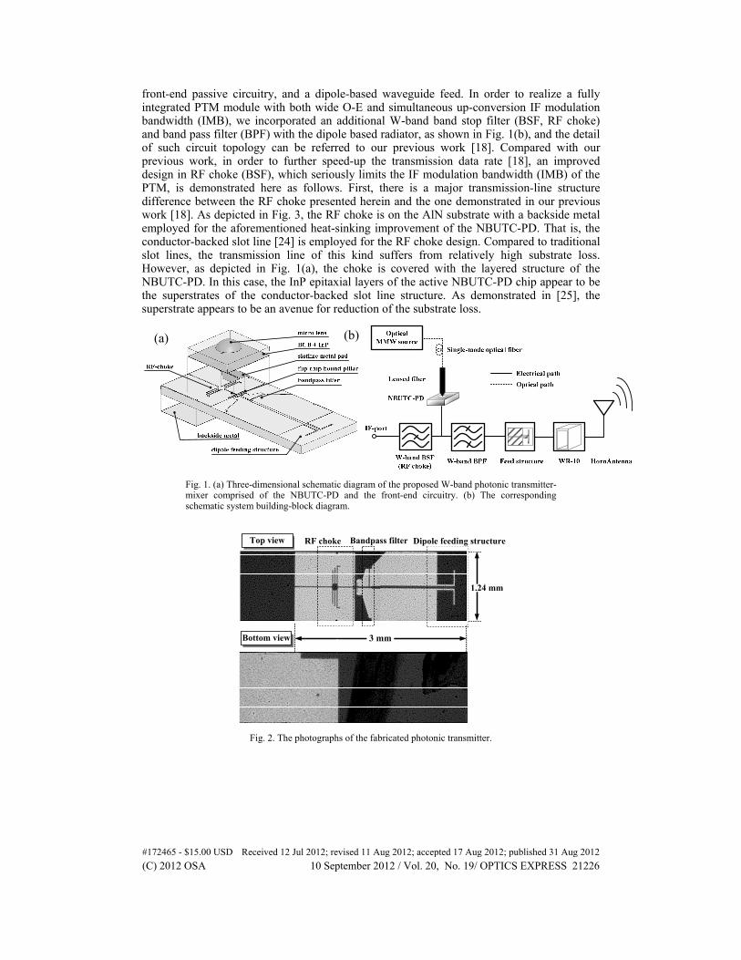
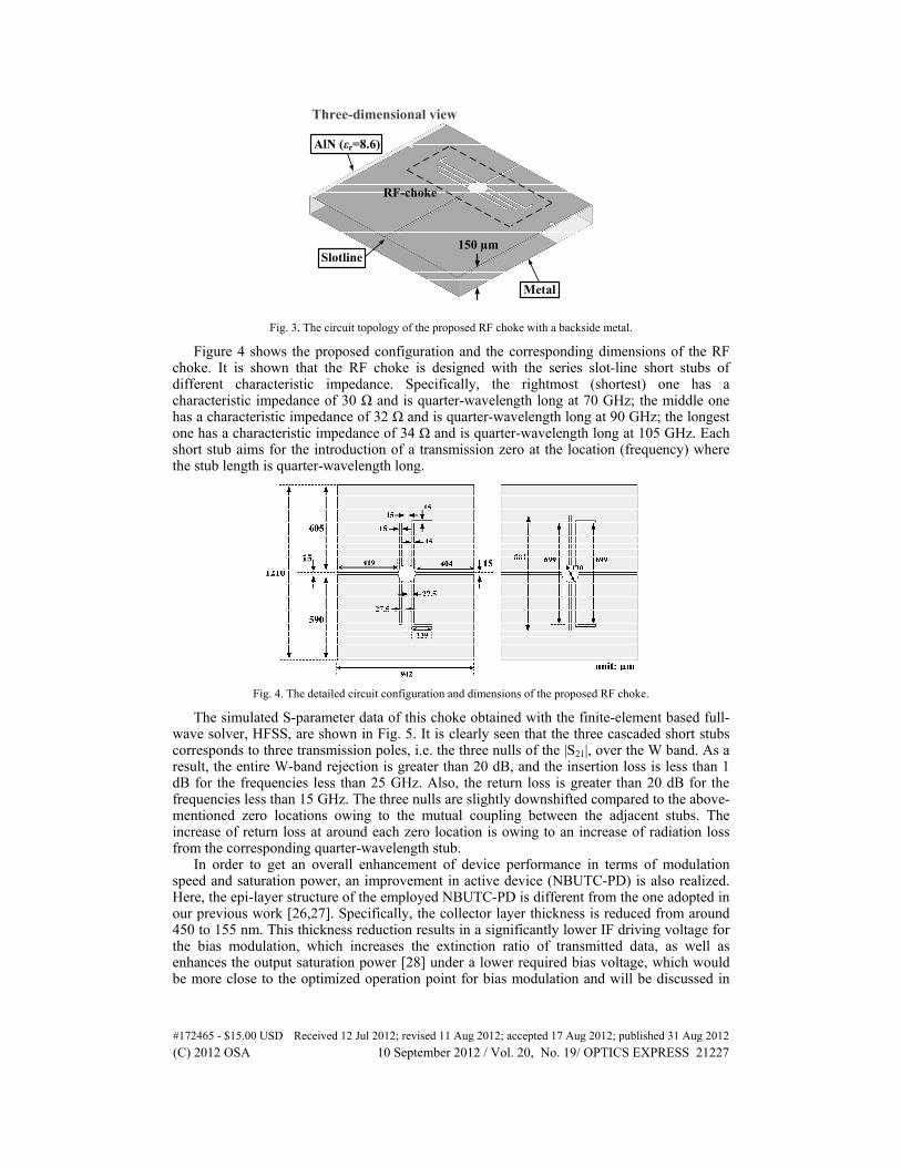
front-end passive circuitry, and a dipole-based waveguide feed. In order to realize a fully integrated PTM module with both wide O-E and simultaneous up-conversion IF modulation bandwidth (IMB), we incorporated an additional W-band band stop filter (BSF, RF choke) and band pass filter (BPF) with the dipole based radiator, as shown in Fig. 1(b), and the detail of such circuit topology can be referred to our previous work [18]. Compared with our previous work, in order to further speed-up the transmission data rate [18], an improved design in RF choke (BSF), which seriously limits the IF modulation bandwidth (IMB) of the PTM, is demonstrated here as follows. First, there is a major transmission-line structure difference between the RF choke presented herein and the one demonstrated in our previous work [18]. As depicted in Fig. 3, the RF choke is on the AlN substrate with a backside metal employed for the aforementioned heat-sinking improvement of the NBUTC-PD. That is, the conductor-backed slot line [24] is employed for the RF choke design. Compared to traditional slot lines, the transmission line of this kind suffers from relatively high substrate loss. However, as depicted in Fig. 1(a), the choke is covered with the layered structure of the NBUTC-PD. In this case, the InP epitaxial layers of the active NBUTC-PD chip appear to be the superstrates of the conductor-backed slot line structure. As demonstrated in [25], the superstrate appears to be an avenue for reduction of the substrate loss.
(a) (b)
Fig. 1. (a) Three-dimensional schematic diagram of the proposed W-band photonic transmitter-mixer comprised of the NBUTC-PD and the front-end circuitry. (b) The corresponding schematic system building-block diagram.
Bandpass filterRF choke Dipole feeding structure
3 mm
1.24 mm
Bottom view
Top view
Fig. 2. The photographs of the fabricated photonic transmitter.
#172465 - $15.00 USD Received 12 Jul 2012; revised 11 Aug 2012; accepted 17 Aug 2012; published 31 Aug 2012(C) 2012 OSA 10 September 2012 / Vol. 20, No. 19/ OPTICS EXPRESS 21226
RF-choke
150 µmSlotline
Metal
AlN (εr=8.6)
Three-dimensional view
Fig. 3. The circuit topology of the proposed RF choke with a backside metal.
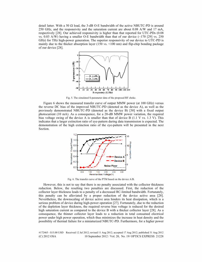
Figure 4 shows the proposed configuration and the corresponding dimensions of the RF choke. It is shown that the RF choke is designed with the series slot-line short stubs of different characteristic impedance. Specifically, the rightmost (shortest) one has a characteristic impedance of 30 Ω and is quarter-wavelength long at 70 GHz; the middle one has a characteristic impedance of 32 Ω and is quarter-wavelength long at 90 GHz; the longest one has a characteristic impedance of 34 Ω and is quarter-wavelength long at 105 GHz. Each short stub aims for the introduction of a transmission zero at the location (frequency) where the stub length is quarter-wavelength long.
Fig. 4. The detailed circuit configuration and dimensions of the proposed RF choke.
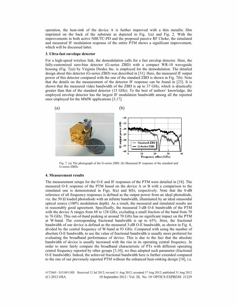
The simulated S-parameter data of this choke obtained with the finite-element based full-wave solver, HFSS, are shown in Fig. 5. It is clearly seen that the three cascaded short stubs corresponds to three transmission poles, i.e. the three nulls of the |S21|, over the W band. As a result, the entire W-band rejection is greater than 20 dB, and the insertion loss is less than 1 dB for the frequencies less than 25 GHz. Also, the return loss is greater than 20 dB for the frequencies less than 15 GHz. The three nulls are slightly downshifted compared to the above-mentioned zero locations owing to the mutual coupling between the adjacent stubs. The increase of return loss at around each zero location is owing to an increase of radiation loss from the corresponding quarter-wavelength stub.
In order to get an overall enhancement of device performance in terms of modulation speed and saturation power, an improvement in active device (NBUTC-PD) is also realized. Here, the epi-layer structure of the employed NBUTC-PD is different from the one adopted in our previous work [26,27]. Specifically, the collector layer thickness is reduced from around 450 to 155 nm. This thickness reduction results in a significantly lower IF driving voltage for the bias modulation, which increases the extinction ratio of transmitted data, as well as enhances the output saturation power [28] under a lower required bias voltage, which would be more close to the optimized operation point for bias modulation and will be discussed in
#172465 - $15.00 USD Received 12 Jul 2012; revised 11 Aug 2012; accepted 17 Aug 2012; published 31 Aug 2012(C) 2012 OSA 10 September 2012 / Vol. 20, No. 19/ OPTICS EXPRESS 21227
detail latter. With a 50 Ω load, the 3-dB O-E bandwidth of the active NBUTC-PD is around 250 GHz, and the responsivity and the saturation current are about 0.08 A/W and 17 mA, respectively [28]. Our achieved responsivity is higher than that reported for UTC-PDs (0.08 vs. 0.03 A/W) having a smaller O-E bandwidth than that of our device (~170 [29] vs. 250 GHz) for THz high-power generation. The superior responsivity of our device to UTC-PD is mainly due to the thicker absorption layer (150 vs. <100 nm) and flip-chip bonding package of our device [28].
Fig. 5. The simulated S-parameter data of the proposed RF choke.
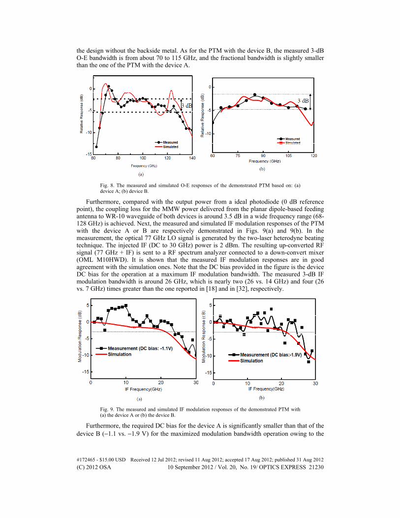
Figure 6 shows the measured transfer curve of output MMW power (at 100 GHz) versus the reverse DC bias of the improved NBUTC-PD (denoted as the device A), as well as the previously demonstrated NBUTC-PD (denoted as the device B) [30] with a fixed output photocurrent (10 mA). As a consequence, for a 20-dB MMW power variation, the required bias voltage swing of the device A is smaller than that of device B (1.1 V vs. 1.3 V). This indicates that a larger extinction ratio of eye-pattern during data transmission is expected. The demonstration of the high extinction ratio of the eye-pattern will be presented in the next Section.
Fig. 6. The transfer curve of the PTM based on the device A/B.
However, this is not to say that there is no penalty associated with the collector thickness reduction. Below, the resulting two penalties are discussed. First, the reduction of the collector layer thickness leads to a penalty of a decreased RC-limited bandwidth. Fortunately, this penalty can be alleviated by a proper reduction of the device active area [28]. Nevertheless, the downscaling of device active area hinders its heat dissipation, which is a serious problem of device during high-power operation [27]. Fortunately, due to the reduction of the depletion layer thickness, the required reverse bias voltage is reduced for the desired high saturation current as compared to the device B with a thicker collector layer [28]. As a consequence, the thinner collector layer leads to a reduction in total consumed electrical power under high power operation, which thus minimizes the increase in heat density and the possibility of thermal failure for a miniaturized NBUTC-PD. Furthermore, for a higher power
#172465 - $15.00 USD Received 12 Jul 2012; revised 11 Aug 2012; accepted 17 Aug 2012; published 31 Aug 2012(C) 2012 OSA 10 September 2012 / Vol. 20, No. 19/ OPTICS EXPRESS 21228
operation, the heat-sink of the device A is further improved with a thin metallic film imprinted on the back of the substrate as depicted in Fig. 1(a) and Fig. 2. With the improvements in both active NBUTC-PD and the proposed passive RF Choke, the simulated and measured IF modulation response of the entire PTM shows a significant improvement, which will be discussed latter.
3. Ultra-fast envelope detector
For a high-speed wireless link, the demodulation calls for a fast envelop detector. Here, the fully-customized zero-bias detector (G-series ZBD) with a compact WR-10 waveguide housing (Fig. 7(a)) by Virginia Diodes Inc. is employed for the demodulation. The detailed design about this detector (G-series ZBD) was described in [31]. Here, the measured IF output power of this detector compared with the one of the standard ZBD is shown in Fig. 7(b). Note that the details on the measurement of the detector IF response can be found in [23]. It is shown that the measured video bandwidth of the ZBD is up to 37 GHz, which is drastically greater than that of the standard detector (15 GHz). To the best of authors’ knowledge, the employed envelop detector has the largest IF modulation bandwidth among all the reported ones employed for the MMW applications [3,17].
(a) (b)
Fig. 7. (a) The photograph of the G-series ZBD. (b) Measured IF response of the standard and G-series ZBDs.
4. Measurement results
The measurement setups for the O-E and IF responses of the PTM were detailed in [18]. The measured O-E response of the PTM based on the device A or B with a comparison to the simulated one is demonstrated in Figs. 8(a) and 8(b), respectively. Note that the 0-dB reference of all frequency responses is defined as the output power from an ideal photodiode, viz. the 50 Ω loaded photodiode with an infinite bandwidth, illuminated by an ideal sinusoidal optical source (100% modulation depth). As a result, the measured and simulated results are in reasonably good agreement. Specifically, the measured 3-dB O-E bandwidth of the PTM with the device A ranges from 68 to 128 GHz, excluding a small fraction of the band from 70 to 76 GHz. This out-of-band peaking at around 70 GHz has no significant impact on the PTM at W-band. The corresponding fractional bandwidth is up to 65%. Here, the fractional bandwidth of our device is defined as the measured 3-dB O-E bandwidth, as shown in Fig. 8, divided by the central frequency of W-band at 93 GHz. Compared with using the number of absolute O-E bandwidth, to use the value of fractional bandwidth is usually more preferred for evaluating the broadband performance of device. This is due to the fact that the absolute bandwidth of device is usually increased with the rise in its operating central frequency. In order to more fairly compare the broadband characteristic of PTs with different operating central frequency reported by other groups [3,10], we thus adopted such parameter (fractional O-E bandwidth). Indeed, the achieved fractional bandwidth here is further extended compared to the one of our previously reported PTM without the enhanced heat-sinking design [18], i.e.
#172465 - $15.00 USD Received 12 Jul 2012; revised 11 Aug 2012; accepted 17 Aug 2012; published 31 Aug 2012(C) 2012 OSA 10 September 2012 / Vol. 20, No. 19/ OPTICS EXPRESS 21229
the design without the backside metal. As for the PTM with the device B, the measured 3-dB O-E bandwidth is from about 70 to 115 GHz, and the fractional bandwidth is slightly smaller than the one of the PTM with the device A.
Fig. 8. The measured and simulated O-E responses of the demonstrated PTM based on: (a) device A; (b) device B.
Furthermore, compared with the output power from a ideal photodiode (0 dB reference point), the coupling loss for the MMW power delivered from the planar dipole-based feeding antenna to WR-10 waveguide of both devices is around 3.5 dB in a wide frequency range (68-128 GHz) is achieved. Next, the measured and simulated IF modulation responses of the PTM with the device A or B are respectively demonstrated in Figs. 9(a) and 9(b). In the measurement, the optical 77 GHz LO signal is generated by the two-laser heterodyne beating technique. The injected IF (DC to 30 GHz) power is 2 dBm. The resulting up-converted RF signal (77 GHz + IF) is sent to a RF spectrum analyzer connected to a down-convert mixer (OML M10HWD). It is shown that the measured IF modulation responses are in good agreement with the simulation ones. Note that the DC bias provided in the figure is the device DC bias for the operation at a maximum IF modulation bandwidth. The measured 3-dB IF modulation bandwidth is around 26 GHz, which is nearly two (26 vs. 14 GHz) and four (26 vs. 7 GHz) times greater than the one reported in [18] and in [32], respectively.
Fig. 9. The measured and simulated IF modulation responses of the demonstrated PTM with (a) the device A or (b) the device B.
Furthermore, the required DC bias for the device A is significantly smaller than that of the device B (−1.1 vs. −1.9 V) for the maximized modulation bandwidth operation owing to the
#172465 - $15.00 USD Received 12 Jul 2012; revised 11 Aug 2012; accepted 17 Aug 2012; published 31 Aug 2012(C) 2012 OSA 10 September 2012 / Vol. 20, No. 19/ OPTICS EXPRESS 21230
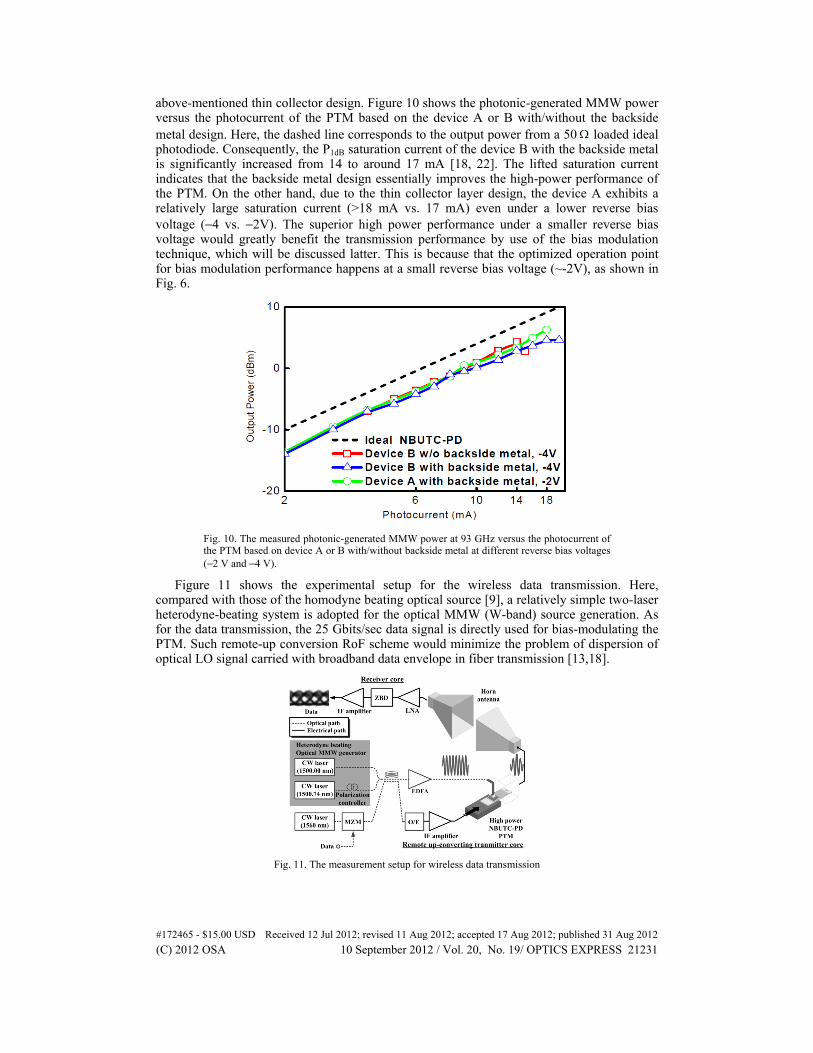
above-mentioned thin collector design. Figure 10 shows the photonic-generated MMW power versus the photocurrent of the PTM based on the device A or B with/without the backside metal design. Here, the dashed line corresponds to the output power from a 50 loaded ideal photodiode. Consequently, the P1dB saturation current of the device B with the backside metal is significantly increased from 14 to around 17 mA [18, 22]. The lifted saturation current indicates that the backside metal design essentially improves the high-power performance of the PTM. On the other hand, due to the thin collector layer design, the device A exhibits a relatively large saturation current (>18 mA vs. 17 mA) even under a lower reverse bias voltage (−4 vs. −2V). The superior high power performance under a smaller reverse bias voltage would greatly benefit the transmission performance by use of the bias modulation technique, which will be discussed latter. This is because that the optimized operation point for bias modulation performance happens at a small reverse bias voltage (~-2V), as shown in Fig. 6.
Fig. 10. The measured photonic-generated MMW power at 93 GHz versus the photocurrent of the PTM based on device A or B with/without backside metal at different reverse bias voltages (−2 V and −4 V).
Figure 11 shows the experimental setup for the wireless data transmission. Here, compared with those of the homodyne beating optical source [9], a relatively simple two-laser heterodyne-beating system is adopted for the optical MMW (W-band) source generation. As for the data transmission, the 25 Gbits/sec data signal is directly used for bias-modulating the PTM. Such remote-up conversion RoF scheme would minimize the problem of dispersion of optical LO signal carried with broadband data envelope in fiber transmission [13,18].
Fig. 11. The measurement setup for wireless data transmission
#172465 - $15.00 USD Received 12 Jul 2012; revised 11 Aug 2012; accepted 17 Aug 2012; published 31 Aug 2012(C) 2012 OSA 10 September 2012 / Vol. 20, No. 19/ OPTICS EXPRESS 21231
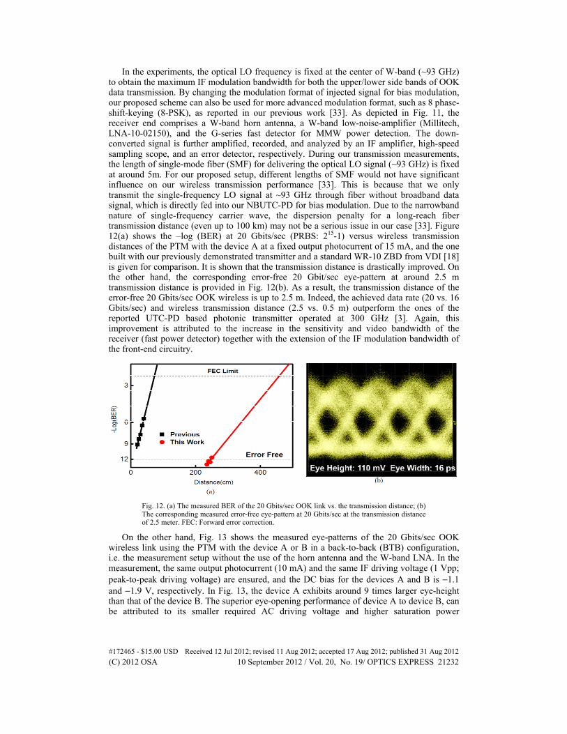
In the experiments, the optical LO frequency is fixed at the center of W-band (~93 GHz) to obtain the maximum IF modulation bandwidth for both the upper/lower side bands of OOK data transmission. By changing the modulation format of injected signal for bias modulation, our proposed scheme can also be used for more advanced modulation format, such as 8 phase-shift-keying (8-PSK), as reported in our previous work [33]. As depicted in Fig. 11, the receiver end comprises a W-band horn antenna, a W-band low-noise-amplifier (Millitech, LNA-10-02150), and the G-series fast detector for MMW power detection. The down-converted signal is further amplified, recorded, and analyzed by an IF amplifier, high-speed sampling scope, and an error detector, respectively. During our transmission measurements, the length of single-mode fiber (SMF) for delivering the optical LO signal (~93 GHz) is fixed at around 5m. For our proposed setup, different lengths of SMF would not have significant influence on our wireless transmission performance [33]. This is because that we only transmit the single-frequency LO signal at ~93 GHz through fiber without broadband data signal, which is directly fed into our NBUTC-PD for bias modulation. Due to the narrowband nature of single-frequency carrier wave, the dispersion penalty for a long-reach fiber transmission distance (even up to 100 km) may not be a serious issue in our case [33]. Figure 12(a) shows the –log (BER) at 20 Gbits/sec (PRBS: 215-1) versus wireless transmission distances of the PTM with the device A at a fixed output photocurrent of 15 mA, and the one built with our previously demonstrated transmitter and a standard WR-10 ZBD from VDI [18] is given for comparison. It is shown that the transmission distance is drastically improved. On the other hand, the corresponding error-free 20 Gbit/sec eye-pattern at around 2.5 m transmission distance is provided in Fig. 12(b). As a result, the transmission distance of the error-free 20 Gbits/sec OOK wireless is up to 2.5 m. Indeed, the achieved data rate (20 vs. 16 Gbits/sec) and wireless transmission distance (2.5 vs. 0.5 m) outperform the ones of the reported UTC-PD based photonic transmitter operated at 300 GHz [3]. Again, this improvement is attributed to the increase in the sensitivity and video bandwidth of the receiver (fast power detector) together with the extension of the IF modulation bandwidth of the front-end circuitry.
Fig. 12. (a) The measured BER of the 20 Gbits/sec OOK link vs. the transmission distance; (b) The corresponding measured error-free eye-pattern at 20 Gbits/sec at the transmission distance of 2.5 meter. FEC: Forward error correction.
On the other hand, Fig. 13 shows the measured eye-patterns of the 20 Gbits/sec OOK wireless link using the PTM with the device A or B in a back-to-back (BTB) configuration, i.e. the measurement setup without the use of the horn antenna and the W-band LNA. In the measurement, the same output photocurrent (10 mA) and the same IF driving voltage (1 Vpp; peak-to-peak driving voltage) are ensured, and the DC bias for the devices A and B is −1.1 and −1.9 V, respectively. In Fig. 13, the device A exhibits around 9 times larger eye-height than that of the device B. The superior eye-opening performance of device A to device B, can be attributed to its smaller required AC driving voltage and higher saturation power
#172465 - $15.00 USD Received 12 Jul 2012; revised 11 Aug 2012; accepted 17 Aug 2012; published 31 Aug 2012(C) 2012 OSA 10 September 2012 / Vol. 20, No. 19/ OPTICS EXPRESS 21232
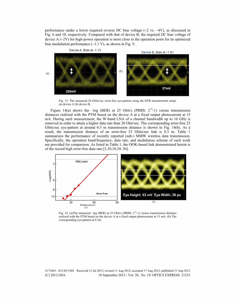
performance under a lower required reverse DC bias voltage (−2 vs. −4V), as discussed in Fig. 6 and 10, respectively. Compared with that of device B, the required DC bias voltage of device A (−2V) for high-power operation is more close to the operation point for its optimized bias modulation performance (−1.1 V), as shown in Fig. 9.
Fig. 13. The measured 20 Gbits/sec error-free eye-pattern using the BTB measurement setup: (a) device A (b) device B.
Figure 14(a) shows the –log (BER) at 25 Gbit/s (PRBS: 215-1) versus transmission distances realized with the PTM based on the device A at a fixed output photocurrent at 15 mA. During such measurement, the W-band LNA of a channel bandwidth up to 16 GHz is removed in order to attain a higher data rate than 20 Gbit/sec. The corresponding error-free 25 Gbits/sec eye-pattern at around 0.3 m transmission distance is shown in Fig. 14(b). As a result, the transmission distance of an error-free 25 Gbits/sec link is 0.3 m. Table 1 summarizes the performance of recently reported (sub-) MMW wireless data transmission. Specifically, the operation band/frequency, data rate, and modulation scheme of each work are provided for comparison. As listed in Table 1, the OOK-based link demonstrated herein is of the record high error-free data rate [3,10,18,34–36].
Fig. 14. (a)The measured –log (BER) at 25 Gbit/s (PRBS: 215-1) versus transmission distance realized with the PTM based on the device A at a fixed output photocurrent at 15 mA. (b) The corresponding eye-pattern at 0.3m.
#172465 - $15.00 USD Received 12 Jul 2012; revised 11 Aug 2012; accepted 17 Aug 2012; published 31 Aug 2012(C) 2012 OSA 10 September 2012 / Vol. 20, No. 19/ OPTICS EXPRESS 21233
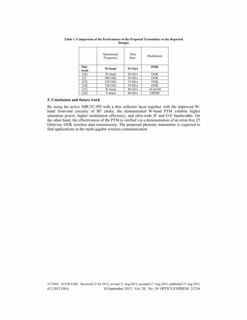
Table 1. Comparison of the Performance of the Proposed Transmitter to the Reported Designs
Operational Frequency
Data Rate
Modulation
This work
W-band 25 Gb/s OOK
[18] W-band 20 Gb/s OOK [3] 300 GHz 16 Gb/s OOK [32] 220 GHz 15 Gb/s OOK [10] 120 GHz 10 Gb/s OOK [33] W-band 40 Gb/s 16-QAM [34] V-band 40 Gb/s OFDM
5. Conclusion and future work
By using the active NBUTC-PD with a thin collector layer together with the improved W-band front-end circuitry of RF choke, the demonstrated W-band PTM exhibits higher saturation power, higher modulation efficiency, and ultra-wide IF and O-E bandwidths. On the other hand, the effectiveness of the PTM is verified via a demonstration of an error-free 25 Gbits/sec OOK wireless data transmission. The proposed photonic transmitter is expected to find applications in the multi-gigabit wireless communication.
#172465 - $15.00 USD Received 12 Jul 2012; revised 11 Aug 2012; accepted 17 Aug 2012; published 31 Aug 2012(C) 2012 OSA 10 September 2012 / Vol. 20, No. 19/ OPTICS EXPRESS 21234


![arXiv:1710.06507v1 [cs.CV] 17 Oct 2017 · Scene Parsing with Global Context Embedding Wei-Chih Hung 1, Yi-Hsuan Tsai , Xiaohui Shen2, Zhe Lin 2, Kalyan Sunkavalli , Xin Lu , Ming-Hsuan](https://img.pdfslide.net/doc/110x75/5f0b686b7e708231d4305ee9/arxiv171006507v1-cscv-17-oct-2017-scene-parsing-with-global-context-embedding.jpg)