Embed Size (px)
Citation preview
Abstract—An integrated Hall sensor was designed and
fabricated in a 0.5μm CMOS ONC5N/F process provided by
MOSIS. On it, four different Hall Plate geometries were
integrated in order to analyze their sensitivity and resistance over
temperature from -40°C up to 165°C. Furthermore, an amplifier
and a current spinning system to remove the amplifier and Hall
Plate offset were designed and placed in the same chip. The
results show a better sensitivity performance in the cross-shaped
Hall Plate and a linear behavior of the sensor in the range of
operation tested.
Resumen—Un sensor Hall integrado fue diseñado y fabricado
en un proceso CMOS ONC5N/F de 0.5μm provisto por MOSIS.
Dentro del mismo, cuatro placas Hall con distintas geometrías
fueron integradas con el objetivo de analizar su sensibilidad y
resistencia desde -40°C hasta 165°C. Dentro del mismo chip
también se integraron y diseñaron un amplificador y un sistema
de rotación de corriente para remover su offset. Los resultados
muestran una mayor sensibilidad en la placa Hall con forma de
cruz y un comportamiento lineal del sensor dentro de su rango de
operación.
Index Terms—Hall Plate, CMOS design, Solid state magnetic
field sensor.
I. INTRODUCTION
A magnetic transducer turns the sensed magnetic field into
voltage. They can be found in many applications such as
printers, TV, scanners, cell phones, camera modules, etc. They
are also very popular in the automotive industry, used for
example, as motor speed control and in the power steering and
lighting system.
A Hall Plate consists of a doped semiconductor section,
defined by a width, a length and a thickness where the Hall
effect takes place. It has two pairs of contacts, one for sensing
and one for biasing. It can be made of different materials, but,
as it will be seen later, lowly doped n-type materials are
normally used.
This paper begins with an introduction to the Hall effect,
where the basic equations are shown. Section III is focused in
Hall Plate offset and the current spinning technique is
presented as a technique used to remove both the Hall Plate
and amplifier offset. In Section IV the Hall Plates designed, its
geometry parameters as well as the amplifier and all the logic
needed to apply the current spinning technique are shown.
Section V shows the measurements made and their results.
Finally, in Section VI the conclusions of the work are
presented.
The integrated circuit was designed using Mentor Graphics
tools under the Higher Education Program (HEP). The chip
was fabricated through the MOSIS foundry service supported
by the MOSIS Educational Program (MEP).
II. HALL EFFECT
The Hall effect was first discovered in 1879 by Edwin Hall
[1]. This effect is the manifestation of the Lorentz Force,
which will appear over mobile charges exposed to an external
magnetic field. This force will push positive and negative
charges in opposite directions causing the appearance of a Hall
electric field and hence a measurable Hall voltage.
When a Hall Plate is biased with a constant voltage (called
voltage driven mode), its sensitivity is defined by [2]
(1)
where is the bias voltage, is known as the geometrical
correction factor of the Hall voltage ( ) [3,4] and
is the Hall Plate resistance, which in the case of a square
geometry can be expressed as
(2)
where and are the width and the length of the Hall Plate
respectively, its resistivity and the electron mobility. In
(1), is called Hall coefficient given, for an n-type
semiconductor, by
where is the electron concentration, is the electron charge
and is the Hall factor [2] which is dependent both on
temperature and scattering mechanism.
Combining (1), (2) and (3), and dividing by the
sensitivity in can be expressed as it is shown in
(4). There, it can be seen that lowly doped n-type materials are
Nicolás Ronis, Mariano Garcia-Inza
Microelectronics Laboratory, Facultad de Ingeniería, Universidad de Buenos Aires
Av. Paseo Colón 850 1st floor, Argentina
Design and Evaluation of a Hall Sensor with
Different Hall Plate Geometries in a 0.5µm
CMOS Process
Revista elektron, Vol. 1, No. 1, pp. 1-7 (2017)
ISSN 2525-0159 1
Recibido: 31/08/16; Aceptado: 19/06/17
preferred since they have a higher mobility and thus, a higher
sensitivity.
(4)
III. OFFSET
An ideal Hall Plate can be modeled as a balanced
Wheatstone bridge which, in absence of magnetic field, will
not show a differential output voltage. However, in a real Hall
Plate a differential output voltage will appear. This unwanted
signal is called offset [5]. Some of its causes are:
Rotations or translations of the masks used in the
fabrication process, which may cause misalignments
in the contacts, avoiding them to be in the same
equipotential line.
Variations in the properties of the contacts due to
errors in the n-plus implantation, which carries errors
in the position, the size and the doping profile.
The crystal lattice suffers disturbances in the
fabrication process. During the dopant implantation,
the lattice can be damaged and contaminants might
be introduced in the silicon. This could affect the
mobility of the carriers.
Taking this into account, the voltage across the bridge can be
expressed as the Hall voltage in addition to the offset voltage.
Furthermore, when an amplification channel is used, its offset
has to be taken into account. In this case, the output can be
expressed as
(5)
where is the amplifier gain, the Hall voltage measured in
a balanced Hall Plate, the Hall Plate offset and the
amplifier offset. To remove the last two, the current spinning
technique was used [6]. It consists of flowing the current in
two opposite directions, called phases, and then averaging the
results. In the next section this technique is explained in detail.
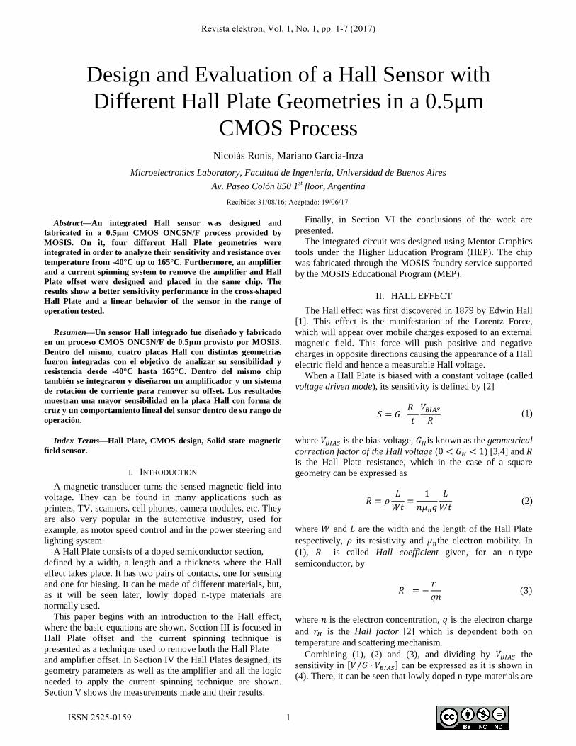
A. Hall Plate Offset
The Fig. 1 shows an unbalanced Wheatstone bridge with the
current flowing in the two phases.
In the case of Fig. 1(a) the voltage across the bridge can be
expressed as
(6)
where
(7)
If now the current is rotated 90° as in Fig. 1(b) the bridge
voltage is
(8)
where
(9)
Since and , the average
of (7) and (9) will remove the offset of the Hall Plate.
Fig. 1. Current spinning technique (a) Phase 90° (b) Phase 0°
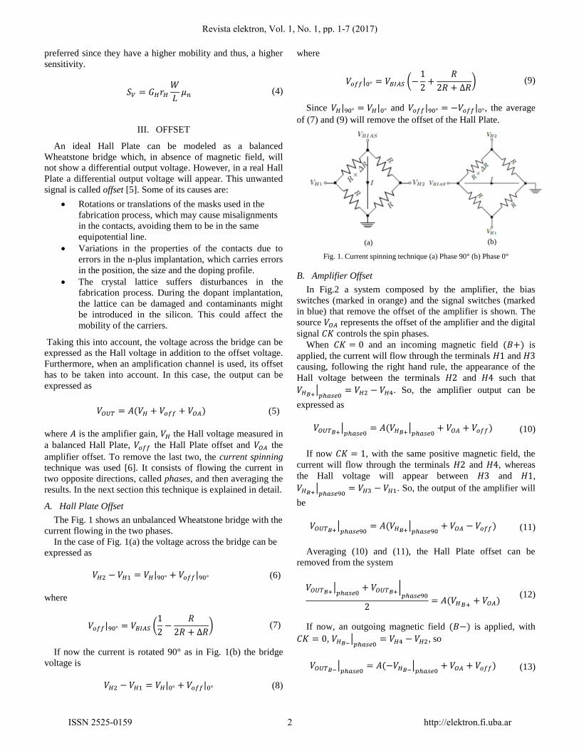
B. Amplifier Offset
In Fig.2 a system composed by the amplifier, the bias
switches (marked in orange) and the signal switches (marked
in blue) that remove the offset of the amplifier is shown. The
source represents the offset of the amplifier and the digital
signal controls the spin phases.
When and an incoming magnetic field is
applied, the current will flow through the terminals and
causing, following the right hand rule, the appearance of the
Hall voltage between the terminals and such that
. So, the amplifier output can be
expressed as
(10)
If now , with the same positive magnetic field, the
current will flow through the terminals and , whereas
the Hall voltage will appear between and ,
. So, the output of the amplifier will
be
(11)
Averaging (10) and (11), the Hall Plate offset can be
removed from the system
(12)
If now, an outgoing magnetic field is applied, with
,
, so
(13)
(a) (b)
Revista elektron, Vol. 1, No. 1, pp. 1-7 (2017)
ISSN 2525-0159 2 http://elektron.fi.uba.ar
Fig. 2. Current spinning system
and with ,
, having at the
output of the amplifier
(14)
Averaging (13) and (14),
(15)
Knowing that the amplifier offset can
be removed using (12) y (15)
(16)
In the present work, the average of the four phases was
done in order to have a better offset removal.
IV. DESIGN
A. Hall Plates
Four different Hall Plate geometries were designed in a
CMOS ONC5N/F process provided by MOSIS.
As it is shown in (4) the mobility plays an important role in
the Hall Plate sensitivity. For this reason, an n-type material,
N-well for this particular process, was selected for the design.
Some important points had to be considered previous to the
design. First, in order to be able to apply the current spinning
technique, the Hall Plates must be symmetrical, which means
that their sensing and bias contacts must be interchangeable.
Second, the contacts should be placed such that they lie in the
same equipotential plane in the absence of external magnetic
field.
The Hall Plates designed can be seen in Fig. 3 and their
geometric parameters in TABLE I.
TABLE I
Geometric dimensions of the Hall Plates designed.
PARAMETER HP1 HP2 HP3 HP4
W [μm] 80 40 80 40
L [μm] 80 40 80 40
W contact [μm] 5.1 39.1 39.1 3.1
L contact [μm] 5.1 3.1 3.1 3.1
Arm [μm] - 40 - -
Fig. 3. Designed Hall Plates in a CMOS process. (a) Big square shape. (b)
Cross-shaped. (c) Orthogonal square shape. (d) Small square shape.
B. Block diagram
In addition to the Hall Plates, the circuits needed to apply
the current spinning technique, to select the desired Hall Plate
and the amplifier stage were designed and implemented in the
same chip.
The Fig. 4 shows the block diagram of the system designed.
The input , accessible from the outside pins
allows us, using two bits, to select the Hall Plate intended to
be measured. Once it is selected, the corresponding HP
LOGIC block, which contains the circuits needed for the
current spinning, is activated. Its block diagram can be seen in
the Fig.5. The block which corresponds to the selected Hall
Plate will have the signal , whereas in the others
this signal will be equal to zero. This was done to disable the
Hall Plate that are not going to be measured so they do not
affect the system. The input , which has a dedicated
pin, is used to bias the Hall Plate.
(a) (b)
(c) (d)
Revista elektron, Vol. 1, No. 1, pp. 1-7 (2017)
ISSN 2525-0159 3 http://elektron.fi.uba.ar
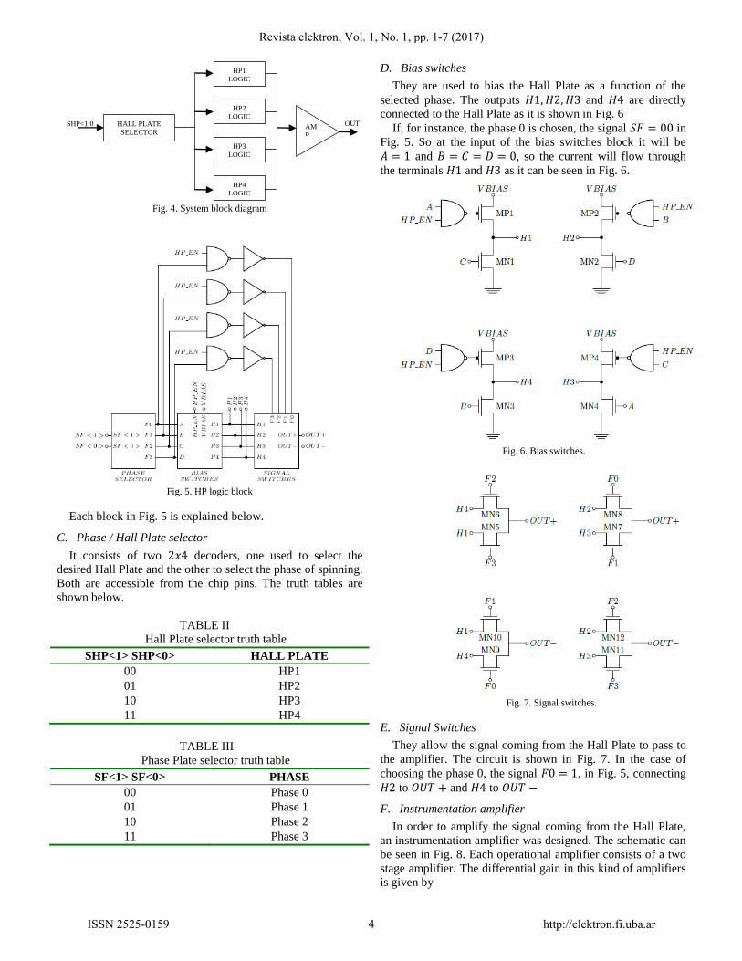
Fig. 4. System block diagram
Fig. 5. HP logic block
Each block in Fig. 5 is explained below.
C. Phase / Hall Plate selector
It consists of two decoders, one used to select the
desired Hall Plate and the other to select the phase of spinning.
Both are accessible from the chip pins. The truth tables are
shown below.
TABLE II
Hall Plate selector truth table
SHP<1> SHP<0> HALL PLATE
00 HP1
01 HP2
10 HP3
11 HP4
TABLE III
Phase Plate selector truth table
SF<1> SF<0> PHASE
00 Phase 0
01 Phase 1
10 Phase 2
11 Phase 3
D. Bias switches
They are used to bias the Hall Plate as a function of the
selected phase. The outputs and are directly
connected to the Hall Plate as it is shown in Fig. 6
If, for instance, the phase 0 is chosen, the signal in
Fig. 5. So at the input of the bias switches block it will be
and , so the current will flow through
the terminals and as it can be seen in Fig. 6.
Fig. 6. Bias switches.
Fig. 7. Signal switches.
E. Signal Switches
They allow the signal coming from the Hall Plate to pass to
the amplifier. The circuit is shown in Fig. 7. In the case of
choosing the phase 0, the signal , in Fig. 5, connecting
to and to
F. Instrumentation amplifier
In order to amplify the signal coming from the Hall Plate,
an instrumentation amplifier was designed. The schematic can
be seen in Fig. 8. Each operational amplifier consists of a two
stage amplifier. The differential gain in this kind of amplifiers
is given by
HP1
LOGIC
HP2
LOGIC
HP3
LOGIC
HP4
LOGIC
HALL PLATE
SELECTOR
SHP<1:0
> AM
P
x10
0
OUT
Revista elektron, Vol. 1, No. 1, pp. 1-7 (2017)
ISSN 2525-0159 4 http://elektron.fi.uba.ar
(17)
where and having an .
Fig. 8. Instrumentation amplifier
Since the gain is defined by the ratio of two resistors, which
are made in the same material, it will not change over
temperature or process.
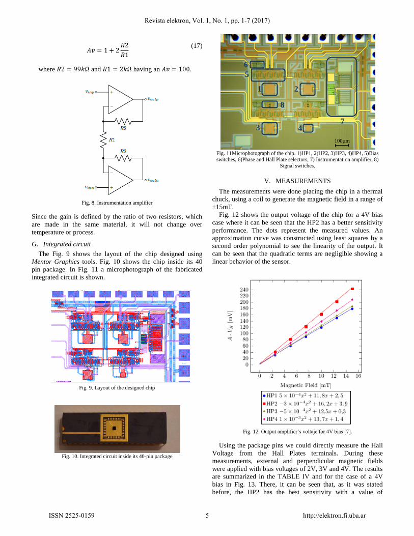
G. Integrated circuit
The Fig. 9 shows the layout of the chip designed using
Mentor Graphics tools. Fig. 10 shows the chip inside its 40
pin package. In Fig. 11 a microphotograph of the fabricated
integrated circuit is shown.
Fig. 9. Layout of the designed chip
Fig. 10. Integrated circuit inside its 40-pin package
Fig. 11Microphotograph of the chip. 1)HP1, 2)HP2, 3)HP3, 4)HP4, 5)Bias
switches, 6)Phase and Hall Plate selectors, 7) Instrumentation amplifier, 8)
Signal switches.
V. MEASUREMENTS
The measurements were done placing the chip in a thermal
chuck, using a coil to generate the magnetic field in a range of
±15mT.
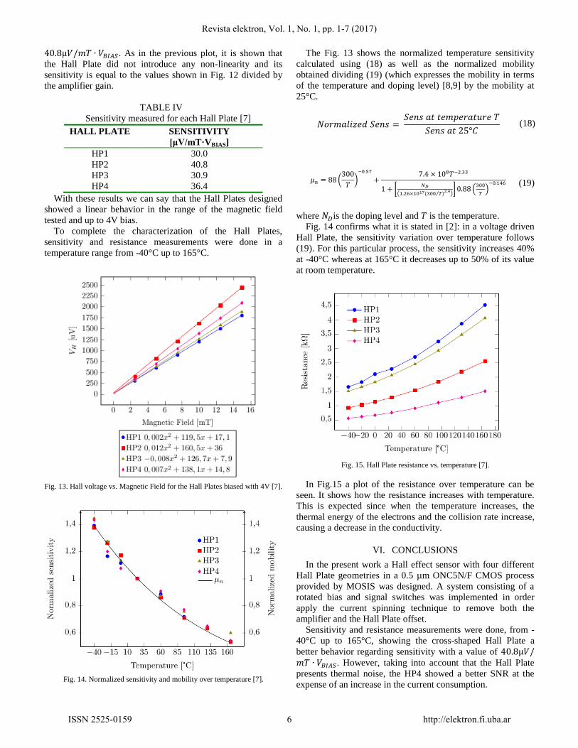
Fig. 12 shows the output voltage of the chip for a 4V bias
case where it can be seen that the HP2 has a better sensitivity
performance. The dots represent the measured values. An
approximation curve was constructed using least squares by a
second order polynomial to see the linearity of the output. It
can be seen that the quadratic terms are negligible showing a
linear behavior of the sensor.
Fig. 12. Output amplifier’s voltaje for 4V bias [7].
Using the package pins we could directly measure the Hall
Voltage from the Hall Plates terminals. During these
measurements, external and perpendicular magnetic fields
were applied with bias voltages of 2V, 3V and 4V. The results
are summarized in the TABLE IV and for the case of a 4V
bias in Fig. 13. There, it can be seen that, as it was stated
before, the HP2 has the best sensitivity with a value of
100µm
1 2
3 4
5
6
7
8
Revista elektron, Vol. 1, No. 1, pp. 1-7 (2017)
ISSN 2525-0159 5 http://elektron.fi.uba.ar
. As in the previous plot, it is shown that
the Hall Plate did not introduce any non-linearity and its
sensitivity is equal to the values shown in Fig. 12 divided by
the amplifier gain.
TABLE IV
Sensitivity measured for each Hall Plate [7]
HALL PLATE SENSITIVITY
[μV/mT·VBIAS]
HP1 30.0
HP2 40.8
HP3 30.9
HP4 36.4
With these results we can say that the Hall Plates designed
showed a linear behavior in the range of the magnetic field
tested and up to 4V bias.
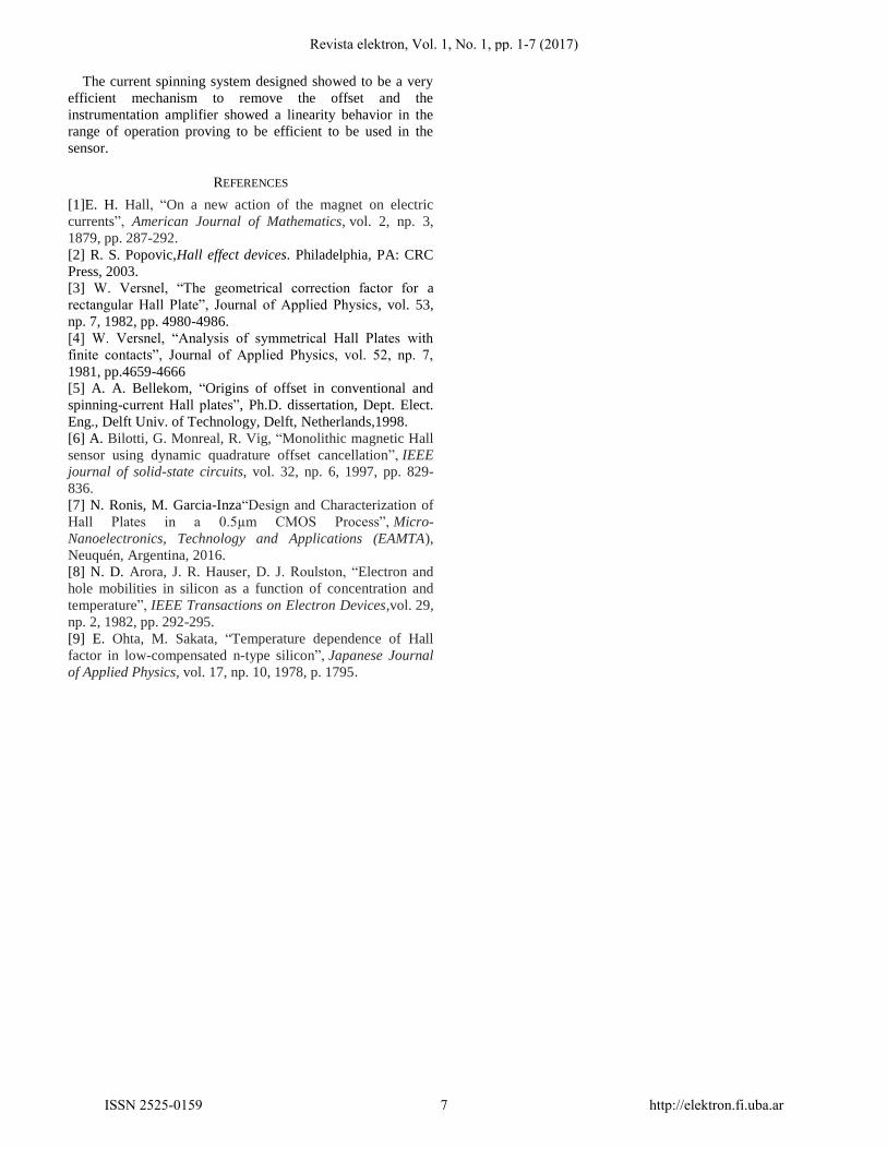
To complete the characterization of the Hall Plates,
sensitivity and resistance measurements were done in a
temperature range from -40°C up to 165°C.
Fig. 13. Hall voltage vs. Magnetic Field for the Hall Plates biased with 4V [7].
Fig. 14. Normalized sensitivity and mobility over temperature [7].
The Fig. 13 shows the normalized temperature sensitivity
calculated using (18) as well as the normalized mobility
obtained dividing (19) (which expresses the mobility in terms
of the temperature and doping level) [8,9] by the mobility at
25°C.
(18)
(19)
where is the doping level and is the temperature.
Fig. 14 confirms what it is stated in [2]: in a voltage driven
Hall Plate, the sensitivity variation over temperature follows
(19). For this particular process, the sensitivity increases 40%
at -40°C whereas at 165°C it decreases up to 50% of its value
at room temperature.
Fig. 15. Hall Plate resistance vs. temperature [7].
In Fig.15 a plot of the resistance over temperature can be
seen. It shows how the resistance increases with temperature.
This is expected since when the temperature increases, the
thermal energy of the electrons and the collision rate increase,
causing a decrease in the conductivity.
VI. CONCLUSIONS
In the present work a Hall effect sensor with four different
Hall Plate geometries in a 0.5 µm ONC5N/F CMOS process
provided by MOSIS was designed. A system consisting of a
rotated bias and signal switches was implemented in order
apply the current spinning technique to remove both the
amplifier and the Hall Plate offset.
Sensitivity and resistance measurements were done, from -
40°C up to 165°C, showing the cross-shaped Hall Plate a
better behavior regarding sensitivity with a value of . However, taking into account that the Hall Plate
presents thermal noise, the HP4 showed a better SNR at the
expense of an increase in the current consumption.
Revista elektron, Vol. 1, No. 1, pp. 1-7 (2017)
ISSN 2525-0159 6 http://elektron.fi.uba.ar
The current spinning system designed showed to be a very
efficient mechanism to remove the offset and the
instrumentation amplifier showed a linearity behavior in the
range of operation proving to be efficient to be used in the
sensor.
REFERENCES
[1]E. H. Hall, “On a new action of the magnet on electric
currents”, American Journal of Mathematics, vol. 2, np. 3,
1879, pp. 287-292.
[2] R. S. Popovic,Hall effect devices. Philadelphia, PA: CRC
Press, 2003.
[3] W. Versnel, “The geometrical correction factor for a
rectangular Hall Plate”, Journal of Applied Physics, vol. 53,
np. 7, 1982, pp. 4980-4986.
[4] W. Versnel, “Analysis of symmetrical Hall Plates with
finite contacts”, Journal of Applied Physics, vol. 52, np. 7,
1981, pp.4659-4666
[5] A. A. Bellekom, “Origins of offset in conventional and
spinning-current Hall plates”, Ph.D. dissertation, Dept. Elect.
Eng., Delft Univ. of Technology, Delft, Netherlands,1998.
[6] A. Bilotti, G. Monreal, R. Vig, “Monolithic magnetic Hall
sensor using dynamic quadrature offset cancellation”, IEEE
journal of solid-state circuits, vol. 32, np. 6, 1997, pp. 829-
836.
[7] N. Ronis, M. Garcia-Inza“Design and Characterization of
Hall Plates in a 0.5µm CMOS Process”, Micro-
Nanoelectronics, Technology and Applications (EAMTA),
Neuquén, Argentina, 2016.
[8] N. D. Arora, J. R. Hauser, D. J. Roulston, “Electron and
hole mobilities in silicon as a function of concentration and
temperature”, IEEE Transactions on Electron Devices,vol. 29,
np. 2, 1982, pp. 292-295.
[9] E. Ohta, M. Sakata, “Temperature dependence of Hall
factor in low-compensated n-type silicon”, Japanese Journal
of Applied Physics, vol. 17, np. 10, 1978, p. 1795.
Revista elektron, Vol. 1, No. 1, pp. 1-7 (2017)
ISSN 2525-0159 7 http://elektron.fi.uba.ar