Embed Size (px)
Citation preview

University of Rhode Island University of Rhode Island
DigitalCommons@URI DigitalCommons@URI
Open Access Master's Theses
2006
Design and Implementation of 8 Bit Successive Approximation Design and Implementation of 8 Bit Successive Approximation
ADC at 1MHZ ADC at 1MHZ
Sesha Smuruti Akkinapally University of Rhode Island
Follow this and additional works at: https://digitalcommons.uri.edu/theses
Recommended Citation Recommended Citation Akkinapally, Sesha Smuruti, "Design and Implementation of 8 Bit Successive Approximation ADC at 1MHZ" (2006). Open Access Master's Theses. Paper 1001. https://digitalcommons.uri.edu/theses/1001
This Thesis is brought to you for free and open access by DigitalCommons@URI. It has been accepted for inclusion in Open Access Master's Theses by an authorized administrator of DigitalCommons@URI. For more information, please contact [email protected].

DESIGN AND IMPLEMENTATION OF 8 BIT SUCCESSIVE
APPROXIMATION ADC AT lMHZ.
BY
SES HA SMRUTI AKKIN AP ALLY
'
A THESIS SUBMITTED IN PARTIAL FULFILLMENT OF THE
REQUIREMENTS FOR THE DEGREE OF
MASTER OF SCIENCE
IN
ELECTRICAL ENGINEERING
UNIVERSITY OF RHODE ISLAND
2006

' APPROVED:
MASTER OF SCIE CE THESIS
OF
SESHA SMRUTI AKKINAPALLY
Thesis Committee:
Major Professor i ~ , nl 7f41 -
~~ DEAN OF THE GRADUATE SCHOOL
UNIVERSITY OF RHODE ISLAND
2006

ABSTRACT
Successive Approximation Analog to Digital converters (ADCs) are very pop-
ular for reasonably quick conversion time and good resolution yet moderate circuit
complexity. This thesis describes the design and implementation of a Successive
Approximation ADC with 8-bit resolution at lMHz speed in 0.5 um CMOS tech
nology. Design, architecture, methodology and performance of the proposed ADC
are presented.
The main features of the Successive Approximation (SAR) ADC architecture de-
signed are very low power dissipation and small chip area because of the compar'
atively simple circuit implementation. The internal Digital to Analog Converter
(DAC) is the most important block of the SAR ADC. Division of Charge im-
plementation was used to realize the DAC to minimize the short-comings of the
conventional charge-redistribution implementation. The SAR ADC was realized
using Switched Capacitor circuitry. The hardware implementation of the schematic
was done in MAGIC and the functionality of the ADC was tested in HSPICE. A
test chip was fabricated and received for verification of the simulation results .

ACKNOWLED GMENTS
It is a pleasure to thank the many people who made this thesis possible.
I thank my major advisor, Dr. Godi Fischer, who helped me right from the
conception of the idea to the very end of the thesis. I am grateful to Dr. Fischer
for his guidance and support throughout the course of study. He is an instructor
par excellence and I am privileged to work under his guidance.
Many thanks to my committee members: Dr Fischer, Dr. Daly and Dr. '
Heskett; as well as my committee chair Dr. Natasha Thomas. I am very thankful
to my professors: Dr. Kumaresan, Dr. Mitra, Dr. Sun and Dr. Davis. I'd also
like to thank everyone I've had the pleasure to study and work with: Prasan,
Vijay, Harini and Partha. I also thank the Department secretaries, Phyllis and
Meredith for their help.
I am grateful to Michael Tedeschi, Edward Zanella, Naveen Lokam and
Marie Crowley for giving me the opportunity to work at ON Semiconductor. I
express my gratitude for their inputs from real world experience.
Finally, I am indebted to my parents, my sister and Bharath for the love
and support they have given through the years. I thank them for giving me
constant encouragement, inspiration and motivation without which my stay in
United States and Master's study would not have been possible.
lll

TABLE OF CONTENTS
ABSTRACT · · · · · · · · 11
ACKNOWLEDGMENTS lll
TABLE OF CONTENTS lV
LIST OF TABLES . . . . . . . . . . . . . . . . . . . . . . . . . . . . . . . vu
LIST OF FIGURES .
' CHAPTER
1 Introduction .
1.1 Goal ..
1.2 Thesis Organization .
List of References . . . . .
2 Introduction to Analog to Digital Converters
2.1 Ideal Analog to Digital Converter (ADC)
2.2 ADC Specifications ... . ... . . .
2.2.1 Static Performance Measures .
2.2.2 Dynamic Performance Measures
2.2.3 Frequency Domain Measures .
List of References .
3 ADC Architectures
3.1 Different ADC Architectures
3.1.1 Flash ADCs
lV
Vlll
1
2
3
3
4
4
6
6
12
13
15
16
16
16

3.1.2 Subranging or Two-Step ADCs
3.1.3 Pipelined ADCs .
3.1.4 Integrating ADCs
3.1.5 Successive Approximation ADCs.
3.1.6 Sigma-Delta ADCs ..... . .
3.2 Comparison of Different Architectures .
3.3 Successive Approximation ADC ....
, 3.3.1 DAC - Based Successive Approximation ADC
List of References . . . . . . . . . . . . . . . . .
4 Design and Implementation of SAR ADC
4.1 Implemented Architecture of SAR ADC . .
4.2 Control Circuitry and Generation of Timing Signals
4.3 Main Blocks of the Implemented SAR .
4.3.1 Accumulator . . . .
4.3.2 Divide by 2 circuit
4.3.3 Comparator ...
4.3.4 Output Registers
5 Layout and Simulation Results
5.1 Layout Considerations
5 .1.1 Floor Planning
5.1.2 Noise Considerations
5.1.3 Matching Issues
5.2 Simulation Results ..
v
Page
18
19
21
23
24
26
27
29
37
38
38
40
43
44
46
53
55
56
56
56
57
58
59

6 Testing and Results . . . . . . . .
6.1 Required Equipment for Testing
6.2 Testing Procedure and Results .
6.3 Conclusion .
List of References
BIBLIOGRAPHY . .
'
Vl
Page
61
61
62
66
68
69

Table
1
2
'
LIST OF TABLES
Performance specifications . . .
Measured Digital output codes
Vll
Page
51
68

LIST OF FIGURES
Figure Page
1 Block diagram representing a Analog to Digital Converter (ADC) [1] . . . . . . . . . . . . . . . . . . . . . . . . . . . . . . 4
2 (a) Transfer Curve for an ideal ADC and (b) its corresponding quantization error [2] . . . . . . . . . . 5
3 Transfer Curve illustrating offset error 7
4 Transfer Curve illustrating Gain error [2] 8
' 5 Transfer Curve illustrating Accuracy [2] 9
6 Transfer Curve illustrating INL error [2] 10
7 Transfer Curve illustrating DNL error [2] 11
8 Transfer Curve illustrating Missing Codes 12
9 SFDR Illustration 14
10 Flash ADC .. . . 17
11 subranging converters 18
12 Pipelined Converters . 20
13 Integrating Converter ADC 21
14 Behavior of Integrating Converter ADC 22
15 Successive Approximation 23
16 Sigma-Delta Converter .. 24
17 Comparison of Different ADC architectures. 26
18 Flow graph illustrating binary search algorithm [2] 28
19 3-bit R-2R ladder DAC . . . . . 29
20 3-bit charge redistribution DAC 31
Vlll

Figure
21
22
23
24
25
26
27
28
29
30
31
32
33
34
35
36
37
38
39
40
41
42
Page
The working of charge division by 2 circuit . . . 35
The implemented architecture of the SAR ADC 38
The conversion process of the SAR ADC . 39
The non-overlapping nature of the clocks . 41
The control circuitry for the generation of non-overlapping clock signals . . . . . . . . . . . . . . . . . . . . . . . . . . . . . . . . 41
The combinational logic implemented to generate the timing signals . . . . . . . 42
' The timing signals 43
The circuit implementation of the Accumulator 44
The divide by 2 circuit implementation . . . . . 47
Simulation results of the accumulator and the divide by 2 cicuit 48
The circuit implementation of the transconductance op-amp . . 49
Simulation results with the performance metrics of the op-amp . 52
The circuit implementation of Latched Comparator. . 53
The simulation results of the comparator . 54
The Floor Planning implemented . . . . . 56
Figure illustrating common centroid layout . 58
The simulation results of SAR ADC 59
Figure illustrating the complete layout with bonding pads 60
DC test set up . . . . . . . . . . . . 62
Graph illustrating the Error in LSB's 63
AC Test set-up . . . . . . . . . . . . 63
Figures Illustrating the SNR of the test chip 65
lX

Figure
43
44
'
Histogram plot . . . . . . . .
FFT of Spice Extracted File .
x
Page
66
67

CHAPTER 1
Introduction
The growth in Digital Computing and Digital Signal Processing in the elec
tronics world is usually referred as " the world is becoming digital day by day."
Digital circuits are less sensitive to the noise and exhibit more robustness to the
increasing variations of the process and supply voltages, they also allow compar
atively easier test automation when compared to the analog circuits. Hence the
informatio\1 is being increasingly stored, processed and communicated in the digi
tal domain [1]. In our physical environment, naturally occurring signals are analog,
hence a device that converts these analog signals to digital form is essential. An
Analog to Digital Converter (ADC) converts a continuous signal into binary infor
mation. Thus, Analog to Digital Converters and their counterparts the Digital to
Analog Converters are critical building blocks or sometimes even bottle necks in
many applications.
An overwhelming variety of ADCs exist in the market today, with different
resolutions, bandwidths, accuracies, architectures, packaging, power requirements,
and temperature ranges, as well as variety of specifications, covering a broad range
of performance needs. There also exists a variety of applications in Data Acquisi
tion, Precision Measurement Applications, Communications, Instrumentation and
Interfacing for Signal Processing etc. Depending upon the application, there is al
ways a "best choice" of a particular type of ADC because of a clear cut advantage
rather than any available ADC model. Thus, there is always an increasing need
for further improvement of available ADC models.
1

1 Goal 1. The objective of this thesis is to design and implement an 8-bit Successive
Approximation Analog to Digital Converter at 1 MHz speed compatible with 0.5um
CMOS process. The main features of this ADC are
• Simple Circuit implementation
• Small Die Size due to due reduced number of capacitors in the internal DAC
• Low power dissipation
• Low to medium supply voltage (2-5V) '
Successive Approximation (SAR) ADC's are preferred to other ADC architectures
due to decreased power dissipation and small chip area because of the compara-
tively simple circuit implementation. The most important block of an SAR ADC
is the internal Digital to Analog Converter (DAC). The linearity of the SAR ADC
depends on the linearity of the DAC unlike the other ADC architectures [2].
Most of the previous implementations of the SAR ADCs used the conventional
R-2R architecture to implement the internal DAC [2]. The R-2R architecture
inherently suffers from DNL (Differential Non-Linearity) and INL (Integral Non
Linearity) errors, due to the mismatch in the resistors comprising the R-2R ladder.
The ADC's are usually classified based on three main features: the Chip Area,
Speed and the Power dissipation. Chip area and the Power dissipation of an R-2R
architecture increase as the resolution increases, due to the large resistor ladder
realized, which also affects the speed of the ADC. In the Literature studied, few of
these draw-backs have been overcome by the Charge-Redistribution implementa
tion [2]. This architecture uses a Programmable Capacitor Array (PCA) to realize
the DAC. As in R-2R architecture, the Capacitor Array grows as the resolution in
creases, thus the power dissipation and the circuit area also increases. Large input
2

capacitance has an effect on the Speed of the ADC, thus this architecture limits
the resolution of the DAC to a maximum of 6-8 bits. The proposed Divide-by-2
Circuit overcomes these limitations. In the proposed architecture, irrespective of
the resolution of the ADC, the number of capacitors required to implement the
Divide-by-2 circuit do not increase. Thus, due to the reduced input capacitance,
the Chip Area and the Power Dissipation are greatly reduced when compared to
the conventional SAR ADC architectures. Speed of the proposed architecture is
also reasonably good when compared to conventional architectures.
1.2 Thesis Organization '
The thesis work is divided into 6 Chapters. Starting with the introduction,
in the chapter l; Chapter 2 illustrates the basic Analog to Digital Converter ADC
and its performance measures. Chapter 3 will talk about the different ADC archi-
tectures available and the different methodologies existing to design a Successive
Approximation ADC. Chapter 4 presents the conversion principle implemented
and will describe the different blocks of the proposed ADC architecture in detail
with the simulation results. Chapter 5 will discuss the layout considerations and
the simulation results of the of the proposed ADC architecture. Chapter 6 de
scribes the Testing procedure of the Test Chip and also presents the measured test
results. Finally, it draws some conclusions.
List of References
[1] B. Razavi, Data Conversion System Design. New York, United States of America: IEEE Press, 1995.
12] K. M. David A. Johns , Analog Integrated Circuit Design. New York, United States of America: John Wiley and Sons, 1997.
3

CHAPTER 2
Introduction to Analog to Digital Converters
The basic definition of an ideal Analog to Digital Converter (ADC) and its
transfer curve are presented in the first part of chapter. The second part of the
chapter classifies and defines different ADC performance parameters. These pa
rameters evaluate ADC's performance and thus help the designer to choose an
appropriate architecture for a specific application.
2.1 IdeAl Analog to Digital Converter (ADC)
The block diagram representing a basic Analog to Digital Converter is shown
in Figure 1. In the figure, Bout is the digital output word, Vin and Vref are the
analog input and the reference signals respectively. The analog input and the
digital output word are related by the following equation.
Where
VisB is defined as the change corresponding to a single Least Significant Bit(LSB)
change.
Vin Bout
ADC
Vref ___ ~J Figure l. Block diagram representing a Analog to Digital Converter (ADC) [1]
4

The input-output transfer curve of an ideal 3-bit ADC is shown in Figure 2(a).
Since the input signal is a continuous signal and the output is discrete, the transfer
curve of the ADC resembles that of a staircase. The Figure illustrates that there
are 2N quantization levels , where N is the number of bits in the digital output.
' (a)
(b)
Digital
output code, B
111
110
101
100
011
010
001
Analog input
Vin 000
0 i/8 ~8 3/8 418 $/8 tt/8 7/8 ~/8 Vref Qe
1 ------------------------- -- - - ----------- ----
~ 0 ~ ..:i
-0.
-1
Vin
Vref
Fig.ure 2. (a) Transfer Curve for an ideal ADC and (b) its corresponding quantization error [2]
5
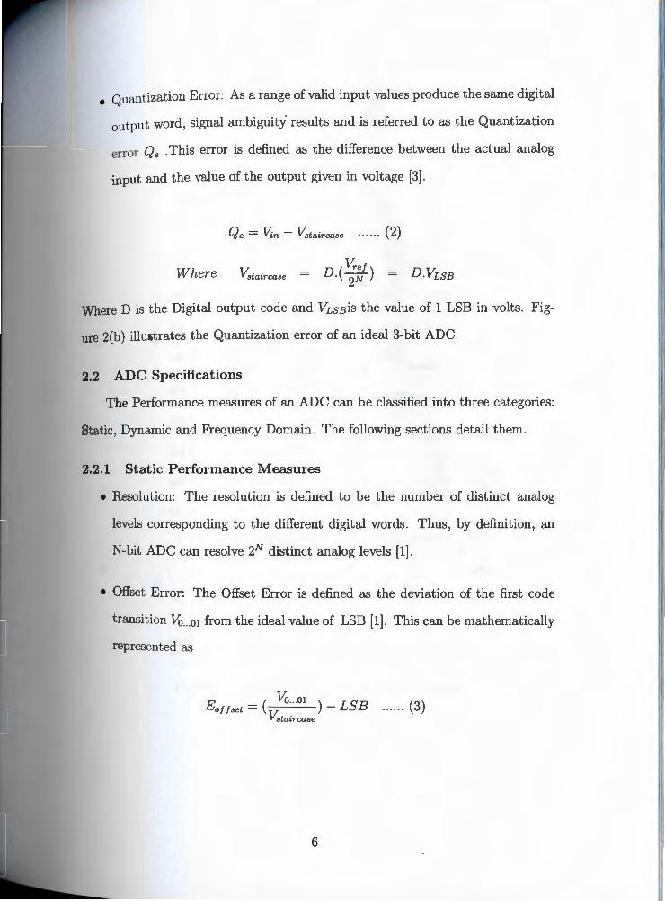
• Quantization Error: As a range of valid input values produce the same digital
output word, signal ambiguity results and is referred to as the Quantization
error Q e .This error is defined as the difference between the actual analog
input and the value of the output given in voltage [3].
Q e = Vin - Vstaircase ····· · (2)
Where ( VreJ) Vstaircase = D. 2N =
Where D is the Digital output code and VLssis the value of 1 LSB in volts. Fig
ure 2(b) iUU11trates the Quantization error of an ideal 3-bit ADC.
2.2 AD C Specifications
The Performance measures of an ADC can be classified into three categories:
Static, Dynamic and Frequency Domain. The following sections detail them.
2.2.1 Static Performance Measures
• Resolution: The resolution is defined to be the number of distinct analog
levels corresponding to the different digital words. Thus, by definition, an
N-bit ADC can resolve 2N distinct analog levels [1] .
• Offset Error: The Offset Error is defined as the deviation of the first code
transition Vo ... 01 from the ideal value of LSB [1]. This can be mathematically
represented as
Vr Eoffset = (.V: o ... Ol ) - LSB ...... (3)
staircase
6

Digital , , , output code, B , , , , , , ,
, , , ,
111
110
101
(a) ' 100
011
010
001
Vin 000
Vref 0 vs 2/8 3/8 418 $18 ~/8 7/8 8/8 Qe
2
1.5 (b)
1 Offset
"' ~ r:ri ~ 0.5
0 Vin --
-0.5 Vref
-1
Figure 3. Transfer Curve illustrating offset error
7

• Gain Error: The Gain error is defined to be the difference at the full-scale
value between the ideal and actual curves when the offset error has been
reduced to zero [1] . The Gain error for an ADC can be mathematically
represented as
'
(a)
(b)
"' =
Egain = [( ;: ... l) - ( ~ .. . Ol )] - (2N - 2) .. ... (4) VLSB VLSB
Digital , '
output code, B , '
111
110
101
100
011
010
001
000
Qe
2
1.5
1
~ ,
0
, , , ,
, , , , , ,
i/8 Z/8
Ideal
"" , , , , , , , , , , , , , , , ,
Actual
3/8 418 $18 618 7/8 818 i i i i
I
Vin
Vref
~ 0.5 r---tlr---i+---+---+__,_---¥_,_----"'-_.____.:.__.__ _ _.___-1--_
0 r--"-----'----'----'----'------'----'--____!--- Vin
-0.5 i-------------------- Vref
-1
Figure 4. Transfer Curve illustrating Gain error [2]
8

• Accuracy: The absolute accuracy of a converter is defined to be the differ
ence between the expected and actual transfer responses [1] . The absolute
accuracy includes the offset, gain and the linearity errors.
Digital
output code, B
111
110
101'
100
011
010
001
000
, ,
, , ,
.-----__. ,
, •'
, , , ,
, , , ,
, , ,
/,.' Total Error --_,__~
• ' At Step 101
/
, , , , (-11/4 LSB)
, ,
,
Total Error At Step 001 (112 LSB)
0 ~/8 ~/8 3/8 418 $/8 ~/8 7/8 8/8
Figure 5. Transfer Curve illustrating Accuracy [2]
9
Vin
Vref

• Integral Nonlinearity Error(INL): The Integral Nonlinearity Error is defined
as the deviation from a straight line (ideal) after the offset and gain error
have been corrected [l]. Conventionally, a "best-fit" straight line is drawn
through the end points of the first and the last code transition to define the
straight (ideal) line. The Figure 5 illustrates the INL.
'
(a)
(b)
Digital
output code, B
111 Straight line through end ,
110 , I
, I
, I , I
,
transitio\ , ',
, /,/ - ~Ideal 101
100
011
010
001
000
Qe
iQ 0 00 ..;i
, ,
0 vs
, ,- -, I
, I , , I
I
~8 ~18 418 $18 ~8 1/8 ws
-0. --------- ---- -- - ---- ____ J ______ _ INL
-1 ------------------------ ----------- -------
Figure 6. Transfer Curve illustrating INL error [2]
10
Vin
Vref
Vin
Vref

• Differential Nonlinearity Error(DNL) : Differential nonlinearity error is dif
ference between the actual code width of a non-ideal converter and the ideal
converter. Figure 6 illustrates the DNL error.
(a) '
(b)
Digital
output code, B
111
110
101
100
011
010
001
, ,
, ,
, ,
000 Vin
"---'--+-~+-~-+-~-+-~-+~----+~~>--~+---V ref 0 vs zis 3/8 41s $18 ~1s 11s ~18
Qe
1 -------------- ------- --- ------- -- ----- -----
=a 0 fZl ~
-0.
-1 -- --------- --------- ----
Figure 7. Transfer Curve illustrating DNL error [2]
11
Vin
Vref

• Missing codes: When no value of input voltage will produce a given output
code, that code is missing from the transfer function and is called the missing
code.
Digital
output code, B
111
110
' 101
100
011
010
001
000
, ,
, ,
Missing code
2LSBs -------, , --------- 7 I , I I , I
, ,
, ,
, , , ,
0 1/8 2/8 3/8 4/8 5/8 6/8 7/8 8/8
Figure 8. Transfer Curve illustrating Missing Codes
2.2.2 Dynamic Performance Measures
Vin
Vref
• Dynamic Range: Dynamic Range is the ratio of the maximum output signal
to the smallest output signal the converter can produce (1 LSB)[3]. Dynamic
range can be written as shown in the following equation.
DynamicRange = 20 log10 (ratio) ...... (5)
12

An N-bit converter has a ratio approximately equal to 2N ,then the Dynamic
range is given by
20log10(2N) = 20Nlog102 = 6.02N(dB) ... ... (6)
• Conversion time: The conversion time of an Analog to Digital Converter
(ADC) , is the time taken for the converter to complete a single measurement
including acquisition time of the input signal [1].
• Sampling rate: The maximum sampling rate is the speed at which samples
can be continuously converted and is typically the inverse of the conversion
' time.
2.2.3 Frequency Domain Measures
• Signal to Noise Ratio (SNR): Signal to Noise ratio is the ratio of the power
of the fundamental and the total noise power excluding the harmonic com
ponents. It is expressed in dB . The SNR accounts for the noise in the entire
Nyquist interval. The SNR can depend on the frequency of the input signal.
It usually diminishes proportional to the input . It can be mathematically
written as
SN R = lOlog( SignalPower ) .... .. (7) Total noise floor power
• Signal to Noise plus Distortion (SNDR): SNDR is the ratio of the funda-
mental and the total noise plus harmonic power. It is expressed in dB.
Mathematically, it can be written as
SN DR= lOlog( . Si~nalPow_er ) ...... (S) noise + armomc power
13

• Effective Number of Bits (ENOB): ENOB measures the maximum signal to
noise plus distortion ratio using bits. The relation between SNDR in dB and
ENOB is
ENOB = SINADdB - 1.76 ... ... (9) 6.02
• Total Harmonic Distortion (THD): THD is the ratio of the power of the
fundamental and total harmonic distortion power. It is expressed in dB.
THD=lOlog( SignalPower ) ... ... (lO) , noise + total harmonic power
• Spurious Free Dynamic Range (SFDR): SFDR is the ratio of the power of
the signal and the power of the largest spurious frequency components. The
SFDR is usually expressed in dB. Mathematically, it can be written as
SF DR= lOlog( f h Signal Power f ) .. .... (11) power o t e largest spurious requency
The figure illustrates the SFDR and other frequency domain parameters.
RMS Fundamental Signal --- ----------- ------------·
Spurious Free Dynamic Range
Largest Spur
Noise Floor
f f N S/2
Figure 9. SFDR Illustration
14

List of References
[1] K. M. David A. Johns, Analog Integrated Circuit Design. New York, United States of America: John Wiley and Sons, 1997.
[2] D. B. R.J Baker, Harry W. Li , CMOS circuit Design, Layout and Simulation. New York, United States of America: IEEE Press Series on Microelectronic Systems, 1998.
[3] E. Cliffs, Devices, Analog-Digital Conversion Handbook. New Jersey, United States of America: Prentice Hall, 1996.
'
15

CHAPTER 3
ADC Architectures
This chapter discusses various architectures available for designing Analog to
Digital Converters and the comparison of different performance measures and trade
offs of different architectures.
Data converters are broadly classified as Nyquist-Rate Converters and Over
sampling Converters depending on the Sampling rate. Oversampling Converters
categorizes data converters with a large Oversampling Ratio, whereas the Nyquist
' Rate converters have a small Oversampling Ratio. The ratio between the Sampling
rate fs and twice the Signal bandwidth is defined as the Oversampling ratio (OSR).
OSR = ! s/2fb ... ... (12)
The basic idea of this thesis is to design and implement a Successive Approximation
ADC, hence popular Successive Approximation ADC architectures are discussed
in the second part of the chapter.
3.1 Different ADC Architectures
As already mentioned, Data converters are classified into two main categories,
Nyquist rate data converters and Over sampling data converters based on the
sampling rate. Flash ADC , Pipelined ADC , Successive Approximation ADC and
Integrating ADC fall under Nyquist rate Data converters. Sigma-Delta ADCs
fall under the Over sampling data converter category. Each has benefits that are
unique to that architecture and span the spectrum of high speed and resolution.
3.1.1 Flash ADCs
Flash ADC's, also known as the parallel ADC's, have the highest speed
compared to other ADC architectures [1] . As illustrated in Figure 10 , a Flash
16

Vin----.
'
R
R/2
Thennomertric Code
E
N
c
0
D
E
R
Figure 10. Flash ADC
DN-1
DN-2
Digital
Output D3
D2 DI
DO
ADC consists of one comparator per quantization level , i.e (2N - 1) comparators,
and a resistor string DAC consisting of 2N resistors, where N represents the
number of bits or the resolution of the ADC. The reference voltage is divided
into 2N reference values by the DAC resistor string, these reference values are
individually compared to the input voltage via a set of comparators resulting in a
thermometer code. Thus , the comparator outputs simultaneously present (2N - 1)
discrete digital states. The thermometric code consists of all zeros for each
resistor level if the reference value is less than the input voltage and all ones, if
the reference value is greater than or equals the input voltage. The thermometric
code is converted into a digital word by using a corresponding encoder.
17

Design considerations and implications
The Flash architecture has the advantage of being very fast, because the con-
version occurs in a single ADC cycle. The advantage of having high speed is
counterbalanced by the requirement of large number of comparators that need
to be carefully matched and properly biased to ensure that the results are linear
[2] . Since the number of comparators needed for an n-bit resolution ADC is
equal to (2N - 1), limits of physical integration and input loading keep the
maximum resolution fairly low. For example, a 16-bit ADC would require 65 ,535
comparato1"; hence Flash ADC's have traditionally been limited to a maximum of
8-bit resolution with conversion speeds of 10 - 40 Ms/s using CMOS technology[2].
3.1.2 Subranging or Two-Step A D Cs
SIU
MSBs
MSB
ADC
v
DAC
Subtracter
Latches
Residue
Amplifier
LSBs
DN-1 DN- 2 D3D2D1DO
Figure 11. subranging converters
LSB
ADC
A Two-Step Flash Converter, also known as a Subranging Converter ,
overcomes few of the limitations of a Flash Converter. Figure 11 illustrates the
basic block diagram of a Two-Step Flash Converter. The Converter essentially
consists of two Flash ADC's separated using a feed forward circuitry. The first
converter generates a rough estimate of the value of the input, and the second
18
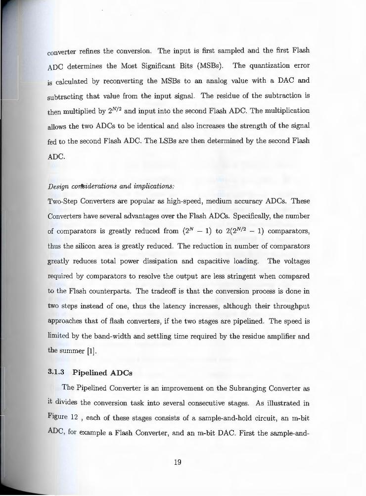
converter refines the conversion. The input is first sampled and the first Flash
ADC determines the Most Significant Bits (MSBs). The quantization error
is calculated by reconverting the MSBs to an analog value with a DAC and
subtracting that value from the input signal. The residue of the subtraction is
then multiplied by 2N/2 and input into the second Flash ADC. The multiplication
allows the two ADCs to be identical and also increases the strength of the signal
fed to the second Flash ADC. The LSBs are then determined by the second Flash
ADC.
Design cor!Biderations and implications:
Two-Step Converters are popular as high-speed , medium accuracy ADCs. These
Converters have several advantages over the Flash ADCs. Specifically, the number
of comparators is greatly reduced from (2N - 1) to 2(2N/2 - 1) comparators,
thus the silicon area is greatly reduced. The reduction in number of comparators
greatly reduces total power dissipation and capacitive loading. The voltages
required by comparators to resolve the output are less stringent when compared
to the Flash counterparts. The tradeoff is that the conversion process is done in
two steps instead of one, thus the latency increases, although their throughput
approaches that of flash converters, if the two stages are pipelined. The speed is
limited by the band-width and settling time required by the residue amplifier and
the summer [1] .
3.1.3 Pipelined ADCs
The Pipelined Converter is an improvement on the Subranging Converter as
it divides the conversion task into several consecutive stages. As illustrated in
Figure 12 , each of these stages consists of a sample-and-hold circuit, an m-bit
ADC , for example a Flash Converter, and an m-bit DAC. First the sample-and-
19

A S/H
D
A ADC/
COMPARATOR
D
+ A
DAC
+ D ~~~~~~~~~~~~~~~~~--1+1--~~~~~--
+
Figure 12. Pipelined Converters
hold circuit of the first stage acquires the signal. The m-bit Flash Converter then
converts the sampled signal to digital data. The conversion result forms the Most
' Significant Bits (MSBs) of the digital output. This same digital output is fed into
an m-bit Digital to Analog Converter (DAC) , and its output is subtracted from
the original sampled signal. The residual analog signal is then amplified and sent
onto the next stage in the pipeline to be sampled and converted as it was in the
first stage. This process is repeated through as many stages as are necessary to
achieve the desired resolution . In principle, a pipelined converter with 'p' pipeline
stages, each with an m-bit Flash Converter , can produce a high speed ADC with
a resolution of N = p x m bits using p x ( 2m -1 ) comparators. For example, a
two stage pipelined converter with 8-bit resolution requires 30 comparators.
Design Consideration and Implications
Pipelined Converters achieve higher resolutions when compared to the Subranging
Converters and the Flash Converters containing a similar number of comparators.
This comes with a price of increasing the total conversion time from one cycle
to 'p ' cycles. But since each stage samples and hold its input , 'p ' conversions
can be underway simultaneously. The total throughput can therefore be equal
to the throughput of a Flash or a Subranging Converter , i.e., one conversion
20

per cycle. The difference is that for the Pipelined Converter , the Latency is 'p'
cycles [1]. Another limitation of the Pipelined architecture is that the conversion
process generally requires a clock with fixed period. Converting rapidly varying
non-periodic signals on a traditional Pipelined Converter can be difficult because
the Pipeline typically runs at a periodic rate.
3.1.4 Integrating ADCs
Clock
fClk = 1
T Clk
Control
Logic
Figure 13. Integrating Converter ADC
21
bl
c b2
0 b3
u N ¢ T
E Bout
R bN

v x
PHASE (I) PHASE (II)
(Constant slope)
Time
T2 (Three values for three inputs)
Figure 14. Behavior of Integrating Converter ADC
Integrating ADCs are a popular approach for realizing high-accuracy data
conversion on very slow-moving signals. These converters perform the conversion
by integrating the input signal and correlating the integration time with a digital
counter. Figure 13 illustrates the basic block diagram of a Dual-Slope ADC.
Dual-Slope refers to this converter since it performs its conversion in two phases.
In phase I, the integration is performed on the input signal and in phase II, the
integration is performed on the reference signal. The input voltage in this case is
assumed to be negative, so that the output of the inverting integrator results in
a positive slope during the first integration. Figure 14 illustrates the behavior of
the Dual-Slop Converter. The first integration is of fixed length, which is decided
by the counter. The sampled signal produces a varying slope. After the counter
is reset , the reference voltage is connected to the input of the integrator. The
inverting integrator output will start to discharge down to zero at a constant slope
as the input is negative with respect to the reference voltage. The counter again
counts the time taken by the integrator to discharge. The final count is equal to
digital value of the input.
22

Design Consideration and Implications
Integrating ADC's are used in high resolution applications but have relatively
slow conversions. These Converters have comparatively low offset and gain errors
in addition to being highly linear. Another advantage of these Converters is that
they have a simple circuit implementation and occupy little silicon area. They are
very inexpensive to produce and are commonly used in slow-moving and low cost
applications like voltage and current meter displays [2].
3.1.5 Successive Approximation ADCs
' SIH
~/A~-----<
Successive-approximation register (SAR) and control logic
b b2 b3 ......................... .
D/A converter
Figure 15. Successive Approximation
Bout
Vref
Successive Approximation ADCs (SAR) have a reasonably good resolution
with quick conversion time. These can be thought of as being orthogonal to the
Flash architecture. While a Flash ADC uses many comparators to convert in
a single cycle; an SAR converter, as shown in Figure 15 , conceptually uses a
single comparator over many cycles to make its conversion. The SAR converter
basically performs a binary search through all possible quantization levels before
converging on the final digital output. To elaborate its operation, in the first
cycle, the Most Significant Bit (MSB) ,b1 , is determined. In the second cycle, the
next bit , b2 , is determined followed by the remaining bits until the N bits of the
ADC are determined. Thus , a straight forward implementation application of an
SAR ADC requires N clock cycles to complete the conversion.
23

Design Consideration and Implications
An SAR converter can use a single converter to realize a high resolution ADC, but
requires N comparison cycles to achieve N-bit resolution, compared to 'p' cycles
for a Pipelined Converter and one cycle for a Flash Converter. SAR Converters
have a relatively simple design and are generally used for low speed and higher
resolution applications. SAR converters are also well suited for applications that
have non-periodic inputs , since conversions can be started at will. This feature
makes the SAR architecture ideal for converting a series of time-independent
signals. '
3.1.6 Sigma-Delta ADCs
~ +·1---In-te-~ C•r::_s_t_,:e_i~m-~-~-:lgi_t~t-;l_An-d~ v-v _ Decimator
1 Bit DAC
Figure 16. Sigma-Delta Converter
Sigma-Delta Converters fall under the Oversampling Converters. As already
mentioned, these converters are sampled at sampling rates much higher than the
Nyquist rate. In its basic form, a Sigma-Delta Converter consists of an Integrator,
a Comparator, and a single bit DAC as illustrated in Figure 16. The output of the
DAC is subtracted from the input signal. The resulting signal is then integrated,
and the integrator output voltage is converted to a single-bit digital output (1
or 0) by the comparator. The resulting bit becomes the input to the DAC, and
the DAC's output is subtracted from the ADC input signal. This closed-loop
process is carried out at a very high "Oversampled" rate. The digital data coming
24

from the ADC is a stream of "ones" and "zeros," and the value of the signal is
proportional to the density of digital "ones" coming from the comparator. This bit
stream data is then digitally filtered and decimated to result in a binary-format
output.
Design Consideration and Implications
One of the most advantageous features of Sigma-Delta architecture is the ca
pability of noise shaping, a phenomenon by which much of the low-frequency
noise is effectively pushed up to higher frequencies and out of the band of
interest [2]. ' As a result , the Sigma-Delta architecture has been very popular
for designing low-bandwidth high-resolution ADCs for precision measurement.
Another advantage is that , since the input is oversampled, the requirement of
anti-alias filtering is greatly relaxed [1] . A limitation of this architecture is its
latency. The latency is caused by the digital filter and is substantially greater
than that of the other architectures.
25

3.2 Comparison of Different Architectures
§!E_P_l_QF_AD_C_S_F:!,-"§~TJQ~ P~QG_E§S
'
Integrating • DelSi
1 Del Si I
14 ------1-------~ - -----,-------r----DelSi DelSi : Pipeline 1
Pipeline 1 Pipeline :
Integrating : 1 1 1 )2 ------J-------L------J-------L----
z 0 f:: :3 IO 0 Cl)
~
SAR SAR
Pipeline Pipeline
-I 5xlOK
Pipeline 1 I
IK
SPEED (samples/sec)
.-------------------------------. 1 FLASH : Upto IO bi t and few hundred Msps 1
I I 1 PIPELINE: 8- 14 bits and Jess that IOOMsps I
1 SAR : 8-12 bits and less that few Msps I I 1 DELSl : High Resolution (12- 16 bi ts) and hundreds Ksps1 •-------------------------------· Figure 17. Comparison of Different ADC architectures.
Figure 17 compares the different architectures of ADC based on the speed of
operation and the resolution that can be achieved. As already discussed, Flash
ADC have the highest speed but at a low resolution due to the increase in the im-
plementation costs with the increase in resolution. Pipelined Converters come next
to the flash ADC's in conversion time with a reasonably good resolution. SAR's
are popular for reasonably quick conversion time yet moderate circuit complexity.
They are also known to have good resolution. Sigma-Delta's that fall under over
sampling converter architecture have a very good resolution at reasonably high
speeds. Thus , depending on the application a particular architecture is a "best
26

choice" specific to that application and as discussed in the previous section, every
architecture has its own advantages and trade-offs. Hence the designer depend
ing upon the application, selects the most suitable architecture for that particular
design.
3.3 Successive Approximation ADC
Successive Approximation ADC employs a "binary search" algorithm in a
feedback loop to determine the closest digital word to match an input signal.
As illustrated in the Figure 15, a Successive Approximation ADC in its most
straight forward implementation consists of a front end Sample and Hold circuit ,
' a Comparator , Control Logic and Decision register and a DAC. During the binary
search , the circuit halves the difference between the sampled and held signal, VIN,
and the DAC output, VD/A, in each clock cycle. Specifically, in the first period,
the decision register is set to mid-scale (100 ... 0) so that the DAC produces a mid
scale analog output. The comparator determines the polarity of ViN - VD/A· This
determines the Most Significant Bit (MSB) , bl. Thus, if VIN > VD/A, the MSB is
set to 1 and if, VIN < VD/A, it is set to 0. In the second period, the decision register
is pointed to (110 ... 0) and the next bit b2 is determined followed by b3, and so on
until all N bits are determined. Thus, in its most straightforward implementation,
a successive-approximation converter requires N clock cycles to complete an N-bit
conversion. A Flow Graph in the Figure 18 illustrates the signed conversion using
the Successive Approximation approach.
27

'
Sample V. m,
START
VD/A =0, i=l
b.= 1 l
Yes
STOP
NO
i+l
b. = 0 l
. 1 VD/A-- V -(V /2 •)
DIA rel
Figure 18. Flow graph illustrating binary search algorithm [2]
28

3.3.l DAC - Based Successive Approximation ADC
A Successive Approximation ADC's performance, employing a DAC in the
feedback path, depends primarily on the DAC's performance. In particular, Dif
ferential and Integral nonlinearity of the ADC are given by those of the DAC,
and the maximum conversion rate of the ADC is limited by DAC's output settling
time. In this section, the different DAC architectures implemented in a SAR ADC
are discussed.
• R-2R Ladder DAC :
A very powlar architecture for DACs use R-2R ladders. This architecture has
the advantage of realizing the binary-weighted currents with a small number of
components and with a resistance ratio of only 2, independent of the resolution
of the DAC. Thus, this architecture has an advantage over conventional Binary-
weighted Resistor DACs. The Figure 19 illustrates the implementation of an R-2R
I Vrefl .._ ~, --7:-----'I':"'"1"2----1-l-Ir l tR -t l -t l 2R
b1 b2 b3
I God
Digital IN from SAR
1nAc -=
2R
Figure 19. 3-bit R-2R ladder DAC
SAR
ladder DAC. The IDAC and IcND currents are maintained at ground potential,
either by the Op-amp summing junction or by a direct connection to ground. The
29

switches steer the current either to the summing junction or to ground depending
on the individual digital logic levels applied to each of the switches coming from
the SAR. For example, logic "high" to b1 will cause the current, In of the Most
Significant Bit (MSB) to add to the !DAG · For a digital " low" the same current
would flow to ground IaND· Since the magnitude of the MSB current is half of
the full scale current it will result in an output voltage that is half of the full scale
output voltage. Thus for a above architecture,
I = VreJ ( 3) T (2R) ... ... 1
And '
...... (14)
Design Considerations: Although, this architecture is an improvement on the con-
ventional binary weighted resistor DAC, it still suffers from few disadvantages.
The Integral and Differential Non-Linearity errors are introduced from the mis-
matches in the resistors comprising the ladder [2].
• The finite 'ON' resistance of the switches add to the resistance of the ladder
network. The switch 'ON' resistance must be much less than the resistance
of the resistors comprising the ladder to maintain high accuracy.
• Another drawback of this circuit is that the currents flowing through the
switches vary widely. To accommodate this, the switches sizes need to be
scaled so that equal voltage drops appear across them for widely varying
current levels.
30

• Charge Redistribution DAC
Vx=O
J_ CJ_
SAR
4C 2C c -= -1...
b1 _l_ h2 _l_ b3 S3 _l_
-::- -= 1. Sample Mode
s
L vref
' CJ_
2. Hold Mode
SI
v __j Vref in °
S3 3. Bit Cycling
s1
V __j Vref in°
Figure 20. 3-bit charge redistribution DAC
31

The newer CMOS DACs implement the Charge Redistribution architecture
to overcome few of the drawbacks of R-2R ladder DAC architecture. The basic
idea here is to replace the input capacitor of a Switched Capacitor gain amplifier
with a Programmable Capacitor Array (PCA) of binary-weighted capacitors. This
approach brings the Sampling mechanism into the DAC architecture , thus the re
quirement for a separate Sample and Hold Circuit is removed. Figure 20 illustrates
the circuit implementation of the charge redistribution DAC. This architecture op
erates in three stages know as the Sampling mode, Hold mode and the Bit cycling
mode.
\
• Sampling mode: This forms the first step of the conversion, the capacitor
array performs the sample and hold operation. In this mode all the capacitors
are charged to Vin while the comparator is being reset to its threshold voltage
through the switch S2.
• Hold mode: In this mode, all the capacitors are switched to ground and the
comparator is taken off the reset mode. Thus, Vx , which was initially zero, is
charged to -Vin , thereby holding the input signal, Vin, on the capacitor array.
Finally, the switch Sl switched to VreJ and VreJ is applied to the capacitor
array.
• Bit cycling: In this mode, the largest capacitor is switched to VreJ , thus
charging Vx to (-Vin + VreJ /2). Now if Vx is negative, then Vin is greater
than Vref /2 , and the MSB capacitor is left connected to VreJ . Thus, the
MSB bl is considered 1, or else the MSB capacitor is reconnected to ground
and bl is taken to be 0. This process is repeated N times, with a smaller
capacitor being switched each time, until the conversion is completed.
32

Design considerations: The main advantages of the Charge-Redistribution DAC
are the higher speeds, the inherent Sample and Hold function, the increased accu
racy and the smaller die size compared to the R-2R ladder architecture. Despite
the advantages, this architecture suffers few disadvantages.
• For high resolutions, the ratio of the largest and the smallest capacitor is
(2N-l), where N is the resolution , as well as the total value of the array
capacitance, can be excessively large. For example, in a 12- bit converter,
the ratio of the MSB and to the LSB capacitor is equal to 2048 , and the
array comprises 4096 equal unit capacitors.
' • The minimum size of the smallest capacitor is often dictated by uniformity
and matching considerations. Hence, the area and the capacitance of large
arrays are huge and this results in an enormous input capacitance for the
converter, which in turn slows down the preceding circuit .
• The Layout gets complicated due to the large capacitor array.
• The large capacitance of the array draws large current spikes from the Ground
and VreJ lines during transients, causing ringing and long settling times in
the presence of inductance in series with these lines [1].
• Charge Division by 2 circuit:
This architecture overcomes few of the drawbacks of the Charge redistribution
architecture. The proposed Divide by 2 circuit, as the name goes, divides the
charge into half the original charge every clock cycle. This operation is repeated
over for N consecutive cycles, where N is the resolution. Figure 21 illustrates
the Divide by 2 circuit implementation. The circuit is realized using a Switched
Capacitor implementation. The operation of the circuit is explained in detail
below:
33

• Phase I: In this phase, switches la and 1 are closed as illustrated in the
figure . During this phase, the first capacitor, C, gets charged to VreJ, while
the Op-amp is being reset to its threshold by closing the switch la.
• Phase II: During this phase the switches 2 and 3a are closed. In this phase,
the Op-amp is taken off the reset mode and the charge across the first Ca
pacitor C, i.e. VreJ, appears at the output of the Op-amp while the second
Capacitor is being discharged to ground.
• Phase Ill: During this phase the switches lb, 1 and 3a are closed. In this
ph3.fie, both capacitors fall parallel to each other. As they have the same
Capacitance C across them, the total capacitance is equivalent to 2C based
on the rule of equivalent capacitance across parallel capacitors. Thus the
total charge across the equivalent capacitance divided by 2, which appears
at the output of the Op-amp.
Phases II and III are repeated consecutively for N cycles, where N is the resolution
of the ADC.
Design Considerations: The main advantages of the Divide by 2 circuit are the
simpler circuitry and the reduced number of capacitors required when compared
to the Charge Redistribution Circuitry. Despite the simple circuitry, one has to
take into consideration the non-linearity introduced due to the following inherent
characteristics of a switched capacitor circuits:
• Capacitor Mismatch: Capacitor Matching forms the most important criteria
in this architecture as the division of charge has to be precise to guarantee
linearity of the division by 2 circuit. Hence the capacitors have to be matched
accurately. Ideally the capacitor size is given by
C = (t:0 x/t0 x)A =Cox· W.L ...... (15)
34

'
c I r I r--1 -1..-4 --lb~--.
3a:l lb r ---'------OUT
112VFS C
O-rel l a
l/2VFS C kC
0~1T i1 ref Vos
la I +
C kC 2 i1 '-----' l"-----''-----'11------i
c 2
la
la
PHASE I
PHASE II
OUT
c PHASE III
OUT
Figure 21. The working of charge division by 2 circuit
35

The mismatch in the capacitors arises from both the oxide thickness gradient
across the surface of the microcircuit and the random variations in length
and width of the capacitor which occurs due to overetching. The error in
troduced due to overetching is usually dominant and can be minimized by
realizing larger capacitors from a parallel combination of smaller, unit-sized
capacitors. Errors due to gradient of the oxide thickness can be minimized by
interspersing the unit-sized capacitors in a common-centroid layout so that
the gradient changes affect both the capacitors in the same way.
• Charge Injection or the Clock Feedthrough: Charge injection or Charge
' Feedthrough error is due to the unwanted charges being injected into the
circuit when the transistors are turned off. When MOS switches are ON,
they operate in the triode region and have zero volts between their drain and
the source. When MOS transistors are turned OFF, charge errors occur by
two mechanisms. The first is due to the channel charge, which must flow
out from the channel region of the transistor to the drain and the source
junctions. The channel charge of a transistor that has zero VDs is given by
QcH = WLCoxVeff = WLCox(Vas - vt) ...... (16)
The second charge is due to the overlap capacitance between the gate and
the junctions. The former error usually dominates unless VeeJ is very small.
The simplest way to make the error due to charge injection small is to use
large capacitors, but large capacitors require a large silicon area. An effective
way to minimize this error is to use fully differential design techniques, but
the tradeoff in using differential circuits is the increase in the complexity of
design.
36

• Offset Voltage of the Op-amp: Input offset voltage of the Op-amp is a source
of error. The input offset error might be caused by device mismatches or
might be inherent in the design of the Op-amp. In Switched Capacitor ap-
plications, this offset voltage can be cancelled by realizing an extra capacitor
at the input of the Op-amp.
List of References
[1] B. Razavi, Data Conversion System Design. New York, United States of America: IEEE Press, 1995.
[2] K. M. David A. Johns, Analog Integrated Circuit Design. New York, United States pf America: John Wiley and Sons, 1997.
37

CHAPTER 4
Design and Implementation of SAR ADC
This chapter presents the implemented ADC architecture. The various build
ing blocks of the implemented ADC are discussed in detail with the simulation
results. The control circuitry and the timing signals required for the proper func-
tioning of the circuit are also presented.
4.1 Implemented Architecture of SAR ADC
' c / I 10
r 3a
11 T
2a la
v~ in la
01
-=
T
lb ~
2b--(8
I~ -=
Q
Q
2
D
c ---~1b--~),__,I~
+ ~b +1· kC C 112YFs
2 1 --0 la ref
Vos 1l
01
la
OUTPUT REGISTERS
OUT
Figure 22. The implemented architecture of the SAR ADC
As already mentioned, switched capacitor techniques are used for the real
ization of the proposed architecture. Accuracy, simple circuit realization , good
38

linearity and dynamic range are few of the reasons for the popularity of switched
capacitor circuitry in last few decades. The basic building blocks of a switched ca
pacitor circuit are op-amps, capacitors, switches and non-overlapping clocks. The
primary advantages of the switched capacitor implementation include compatibil
ity with CMOS technology, good accuracy of time constants, good voltage linearity
and good temperature characteristics. Despite the advantages of the switched ca
pacitor circuits, there are few draw-backs. Clock feed-through and requirement of
non-overlapping clocks fall under disadvantages of switched capacitor circuits.
The implemented architecture is shown in the Figure 22. As illustrated in this
Vmax
2
' . : :
t T T ---------------- · NT b3= 1
bi=O b:...l 4
Figure 23. The conversion process of the SAR ADC
t
figure , the proposed architecture consists of three main blocks: An Accumulator,
a Comparator and a Divide by 2 circuit. As already discussed in chapter 3, the
Successive Approximation ADC 's apply the binary search algorithm to determine
39

the closest digital word to match an input signal. The proposed architecture im
plements the binary search algorithm by dividing the charge into half the original
charge every clock cycle. The accumulator, then depending on the previous cycle's
comparator output, either accumulates or subtracts the residual charge from the
original charge; if the previous cycle's comparator output equals '1', the charge
gets accumulated to the original charge and if the output equals 'O', the charge
gets subtracted from the original charge. The output of the accumulator is then
fed into the comparator, which determines the digital equivalent of the analog in
put. This process is repeated for N consecutive cycles, where N is the resolution of
the ADC. 1'he Figure 23 illustrates the conversion process of the proposed ADC
architecture.
4.2 Control Circuitry and Generation of Timing Signals
In this section the control circuitry required for the functioning of the proposed
ADC architecture is presented. As already mentioned in the preceding section, non
overlapping nature of the clocks is very critical for the functioning of the switched
capacitor circuits. These clocks determine when charge transfers occur and they
must be non-overlapping in order to guarantee charge is not inadvertently lost.
The term non-overlapping clocks refers to two logic signals running at the same
frequency and arranged in such a way that at no time both signals are high as
illustrated in the Figure 24.
40

Ct
voNI /\ VoFF !\., •o•r :n !
V OFFr ' L___j '
T
/\ 0 ' '
In Figure 24. The non-overlapping nature of the clocks
Figure 25 illustrates the implemented control circuitry for the generation of
non-overlapping clocks.
'
Clk 3Bit
Counter
Clk
C3 Q D
2
2
1a
1a
~---3a
Figure 25. The control circuitry for the generation of non-overlapping clock signals
41

The control circuitry illustrated generates four sets of non-overlapping clocks
using a master clock signal CLK. Even numbers of inverters are implemented to
introduce a delay, which ensures the non-overlapping nature of the clocks. The
asynchronous three bit counter is realized using T flip-flops . To realize the counter,
the flip-flops are connected in cascade; with the first T flip-flop triggered by the
master clock CLK and the remaining are triggered by the previous flip-flop 's out-
put . The term asynchronous is used as all the flip-flops are not triggered using the
master clock CLK. The non-overlapping clocks, thus generated are used for the
generation of timing signals required for the functioning of the SAR ADC. The
combinati~nal logic implemented for generation of the control signals is illustrated
in the Figure 26. Figure 27 illustrates the simulation results of the control circuitry
and the combinational logic implemented.
C3 C2
C3
Cl
C3 C2
2a
2a
: 1 b
1b
Figure 26. The combinational logic implemented to generate the timing signals
42

inp,1 M : ~I)
s.o~~---------,~~
~~ ru ~.o ···················---··························--·--·--··--·····--······················ ................................................................ + ............................................................................................................................... M : ~•I
s.olnnn-~Flnnnri~ ~ uj
::~=~~~·! ~ ~o P2
o.o ........................................................................................................................................................... 1 ................................................................................................................................ M : ~s)
,:L _ -- _:::- J~ ---------- _[ ,:b · '~I n I~
D I M~
,lhJ'.itQjJj:~L _______ tbdM~ ,:I ~ _ titQJd~ ': .. "'I ==;=-.. r .. -... = ...... =r ...... = ...... = ..... 'F ...... = ...... ""' ...... = ...... = ...... ;= ..... = ...... "'i" ...... = ...... = ...... ;= ...... = ..... T ...... = ...... =i ...... = .. :=.3.~Tlu= ...... =i ...... = ...... = ...... "j= ..... = ...... , ...... = ...... = ...... r ..... = ...... =r ...... = ...... = ...... 'F ..... = ...... =r ...... = ...... = ...... r= ..... =-r
u ~ ~ ~ ~ ~ ~ ~ ~ ~ ~ ~ ~ ~ ~ ~ ~ & ~ ~ ~
l•I
Figure 27. The timing signals
4.3 Main Blocks of the Implemented SAR
The design of data conversion systems deals with both architectural issues
and circuit level considerations. The choice of architecture is influenced by the
performance of its constituent building blocks. The trade-off's that occur at each
level of abstraction often determine the performance of the complete architecture.
In this section, the implementation of the main building blocks of the SAR ADC
is discussed. The main building blocks of the proposed SAR ADC are
• Accumulator
43

• Divide by 2 circuit
• Comparator
These building blocks of the SAR ADC are discussed in detail with the simulation
results in the following section.
4.3.1 Accumulator
c ,__I -r-~/-~
3a
11
OUT
Figure 28. The circuit implementation of the Accumulator
The Figure 28 illustrates the circuit implementation of the accumulator. As
illustrated in this figure, a switched capacitor based accumulator design is con
sidered. As already discussed in the section 4.1, the accumulator based on the
comparator output either accumulates the charge or substrates the charge form
the input charge. Despite the simple implementation of the circuit , there are few
design considerations to be taken into account when designing switched capacitor
integrator circuits.
• Implementation of the switches: CMOS switches are implemented. The ad-
vantage of CMOS transmission gates over the conventional NMOS switches
is that they have less ON-resistance. The settling behavior of the switched
capacitor depends on the total capacitance and the ON-resistance of the
44

switches, T =CL* RoN, thus CMOS implementation helps in having a bet
ter op-amp settling behavior. In addition to the lesser ON-resistance, they
allow a wider swing of the signals and the error introduced because of the
charge injection is less in the CMOS implementation when compared to the
NMOS implementation.
• Charge Injection Error: The MOS switches exhibit channel charge injection
and clock feedthrough. When the MOS is ON, a certain amount of charge
is present in its channel. When the MOS is turned off, the principle of
charge conservation dictates that this channel charge gets redistributed and
' accumulates in the source and drain terminals. This introduces an error in
the sampling capacitor, which is also referred as the clock-feedthrough. Use
of large capacitors reduces the error due to charge injection. The effect of
larger capacitors will be discussed in the next point.
• Size of the Capacitors: As already mentioned, the error due to charge in-
jection is minimized by using larger capacitors but this is counter-balanced
by increase in the total capacitance of the circuit which again has an impact
total performance of the op-amp. Use of larger capacitance also increases the
silicon area. Hence the size of the capacitors used has to be optimized, so
that the performance of the accumulator is not affected. The size of the ca-
pacitors implemented for the proposed design is 0.8 pF, taking into account
the above design considerations.
• Op-amp offset voltage: Finally the error introduced due to inherent op-amp
offset voltage has to taken into consideration. This error at the end of the N
iterations is given by
ECos = (1 - 2)-NVos ...... (17)
45

Where Vos is the offset voltage of the Op-amp. This error can be minimized
by implementing an extra capacitance in series with the negative input ter
minal of the op-amp. This capacitor then gets charged to Vos, the offset
voltage of the op-amp and thus cancels it out.
From the above design consideration, it can be concluded that use of larger
( w /1) ratio for the switches lowers the RoN of the switches and thus im
proves the settling behavior of the op-amp, but increases the error due to
the clock-feedthrough as larger switches accumulate larger channel charges.
Hence there is a trade-off in selecting the (w/1) ratio of switches. For the
propbsed design the size of switches implemented is (9/2).
4.3.2 Divide by 2 circuit
The Figure 29 illustrates the Divide by 2 circuit implementation. As the
functionality of the divide by 2 circuit has already been in Chapter 3, it will not
be dealt here to avoid redundancy. As the figure illustrates , a switched capaci
tor implementation is used for the design of the divide by 2 circuit also. Hence
all the design considerations, discussed in case of the accumulator section, apply
here. Thus, taking the various design consideration into account , the sizes of the
capacitors and the switches realized is 0.8 pF and (w/1) = (9/2) respectively. The
precise matching of the capacitors is very critical to achieve an accurate division
of charge. Hence the error introduced due to improper matching of the capacitors
should be taken into account. If it is assumed that the capacitors are matched
with an error t:, then the total error introduced can be calculated as follows.
From phase I, the total charge in the circuit is equivalent to
Q = VrefC ..... . (18)
From phase II ,
Vout = VreJC ...... (19)
46

'
c ~I
4
I
1+~ li2YFs ~ kC 0-- 2
~ '" )' Voo la
::- ::-
112VFS
0 ref
::- ::-
~~
lb
la
PHASE I OUT
PHASE II
PHASE III
Figure 29. The divide by 2 circuit implementation
From phase III , both the capacitors are in parallel. Considering the second capac-
itance value is equal to (1+ E) C, the total capacitance is equivalent to (2+ E) C.
Hence
Vout(2 + E)C = VreJC ... ... (20)
Thus, Vout = VreJ/(2 + E) ...... (21)
47

Simplifying the about equation using the Taylor 's formula, we get
( '1reJ 1 Vaut = -
2- )(1 - 2E) ...... (22)
Repeating the above calculation of N cycles, where N is the resolution, we get the
error introduced due to mismatching is given by ( ~;/) * (1 - Jf E).
The ways of minimizing the mismatch errors in the capacitor layout are discussed
in Chapter 5 under layout considerations. Figure 30 illustrates the simulation
results of the divide by 2 circuit and the accumulator implemented.
M : ~aJ 2.0 ,~-----------------------------v(o2,pJ
1.0
Integrator output
~ O.Ol~------.-1
.,.
2.0"····················································••oO••• ·································································································································································································································J M : ~aJ
3.0 ,~----------------------·-------- v(o\,J'll
0
0
0
·2.0
Divide by 2 circutt
·····················-·-···-········-·--·· .......................................................................................... ···········································-··-·-·································---·····-·-·---·--··-·· ............... M : ~aJ
v("#W)
Input Signal
L_
~ ~ - - - . ~ ~ ~ ~ ~ ~ ~ ~ ~ ~ ~ ~ qa)
Figure 30. Simulation results of the accumulator and the divide by 2 cicuit
48

Op-amp
+Vdd
R
15/4
bn2 m9
9013
-Vss
2X( l50/3)
2X( l50/3)
+In Out
r--0 150/4
m13 2X(90/4)
2X(90/4)
Figure 31. The circuit implementation of the transconductance op-amp
The performance of the operational amplifier is very crucial for precise func-
tioning of the divide by 2 circuit and the accumulator and hence affects the total
performance of the ADC. Although, op-amps were traditionally designed to have a
gain of several hundred thousand and to provide relatively low output impedance,
they have evolved into different topologies, as they are used as fundamental build-
ing in a variety of analog circuits. Various performance metrics like gain, slew rate,
dynamic range and power dissipation dictate the choice of the op-amp topology to
be considered for a particular application. Previous literatures show that transcon
ductance operational amplifier is a good choice for switched capacitor circuits as
the load is purely capacitive. Due to reasonably high speed and good bandwidth
consideration, a current mirror transconductance op-amp configuration is selected.
49

Figure 31 illustrates the CMOS transconductance amplifier implemented. As the
figure illustrates , the transconductance operational amplifier has three stages, the
bias stage, the differential gain stage and the push pull output stage.
The settling requirements of the op-amp outputs determine unity-gain band-width
(UGB) and slew rate for the given clock frequency and capacitive loads. The min
imum necessary slew rate for linear settling depends on the maximum step in the
op-amp output voltage and linear settling time-constant. It is a know fact that the
settling time constant depends on the total capacitance of the circuit. In the case
of the accumulator circuit, during the phase when the switches 2, 2a and 3a are
closed the to~al capacitance seen by the op-amp is 2(C/3). During the phase when
the switches lb, 1 and 3a are closed, the total capacitance appearing is equal to
C/2. Hence considering the worst case scenario the total capacitance that appears
on the op-amp in the case of the accumulator is given by
CL= 2c2 /3C = 2C/3 + Ccs .. .... (23)
Where Casis the gate capacitance of the preceding circuitry. In case of the divide
by 2 circuitry, as illustrated in Figure 28 , as the circuit operates in 3 phases as
discussed in chapter 3, the load capacitance is phase 2 and phase 3 is given by C 2 /2
and 3C/2 respectively. Considering the worst case scenario, the load capacitance
at the output of the op-amp is given by
CL = (C2 /2C) + C = 3C/2 + Ccs .. .... (24)
As the capacitors implemented in the design of the accumulator and the divide by
2 circuit are equivalent to 0.8 pF. The op-amp required for the implementation of
accumulator and the divide by 2 circuit should be able to drive a total capacitive
load equivalent to at least 1.5 pF. Thus considering the worst case scenario of
having a larger load capacitance on the op-amp, the op-amp to be designed has
50

to have the specifications of de gain, unity gain bandwidth (UGB), phase margin
and slew rate of about 70 dB, 100 MHz, 50 MHz respectively.
PARAMETERS VALUE
VDD, Vss + 2.5, -2.5 respectively DC Gain 77.102 dB Unity-Gain Bandwidth (UGB) 104.53 Phase Margin 58 MHz Positive Slew Rate 88.6 V /us Negative Slew Rate 68.43 V /us
Table 1. Performance specifications
The device \limensions of the transistors considered and the architecture of the
op-amp implemented are illustrated in the Figure 30. The simulation results of
the designed op-amp are illustrated in the Figure 32. Table 1 lists the simulation
results obtained from the designed op-amp at capacitive load of 1.5 pF. Thus, from
the simulation results it can be comprehended that the designed op-amp meets the
desired specifications.
51

-dog))'lt>tz)
0.0 "'·' ,,-----=··""····""-···:::.:··-=······················································· ··························-··············· ·· -
(14.417, 77.102)
·20.D 70.0 1
"·' ....
.... , "·'1
... , 5' i I -eo.o iif
" 1 !,.
-100.0
~·'1
20.I
·120.0 ' ·140.0
"'I D• I
·1 50.0 -10.0 ·················································· ····--····
10.0 30.0 100.0 300.0 1.mt Ult 10.rlt 30.lt 100.111 300.tll. trneg - 1Dmlg 3Dmlg 10Clmlg 30llr""!I lt>tz)
.... , M,q,1
.,,,~~~~~~~~~~~~~~~~~~~~~~~~~~~~~~~~~~~~~~~o')
ID I
'·'1 ~ Positive slew-rate • 88.6 Vlljs Negative slew-rate • 68.43 /us
.,.
·2.0
\..
.. ···············-·························· ····················-··············· ································-································· ························-··················· M,q,1 ... ~~~~~~~~~~~~~~~~~~~~~~~~~~~~~~~~~~~~~-,"",
~ ,. Input Signal
·2.0
-4.0 I .................................................. T""'' ...................................................... ,. ,, .. "' .. "
Figure 32. Simulation results with the performance metrics of the op-amp
52

4.3.3 Comparator
Vdd NClk
ol m7
Out
ml6
Fig~re 33. The circuit implementation of Latched Comparator.
The Comparator forms an important component of the SAR ADC, as the
performance of the ADC partly depends on the performance of the comparator. A
comparator can be thought of as a fast , high gain op-amp which is not used with
negative feedback, which compares one analog signal with another analog signal
and outputs a binary signal based upon the comparison. A variety of approaches
are available to design a comparator but recent studies show that latched com
parators are a better choice for modern high speed CMOS applications. Hence
the latched architecture was selected for the implementation of the comparator. A
latched comparator consists of a preamplifier stage and a latch stage that has two
modes of operation: tracking and latching. In the tracking mode, the preamplifier
is enabled to amplify the input difference and tracks the input , while the latch is
disabled. In the latching mode, the preamplifier is disabled and the latch and the
positive feedback are enabled, so that the instantaneous output of the preamplifier
is repeatedly amplified and the positive feedback regenerates the analog signal into
a full-scale digital signal.
Figure 33 illustrates the comparator circuit implemented in the proposed ADC
53
I
I

...... M ' l(ol ... ~~~~~~~~~~~~~~~~~~~~~~~~~~~~-~~
OUTPUT SIGNAL
~ 0.0
-6.0 .......•........•.•...••.••• ...............••...•.•..• ····································-·······································-········- ··············-············ ..........•.••.••.•••.•••.•••••.•••. M :l(•I ... ~~~~~~-~~~~~~~~~~~~~~~~~~~~~~--~ CLOCK-SIGNAL
~ a.a
.s.o ···································•·•······•···•··········• .................................................. ·····································•··•····•··· ...
~ a.o
II--
' INPUT SIGNAL
~ --····· ························· ················ ·· ·· ···· ····· ··········· ·············· ··· ········· ·················· ·· · ····· ·· ·· ······ ·· ··············· · · · ····· ······· ····--·· ···· - ...
Figure 34. The simulation results of the comparator
........................... M :tf•I
""'
,,
design. The output of the accumulator becomes one of the inputs to the com-
parator and the other input is grounded. Two important performance metrics of
the comparator to be considered for the precise operation of the SAR ADC are
the comparison rate and the kick back noise. Kick back noise is the power of the
transient noise observed at the comparator input due to switching of the amplifier
and the latch. As the considered architecture has a preamplifier stage, the effect
of the kick-back noise is eliminated. The Figure 34 shows the simulation results
of the considered regenerative latched comparator. From SPICE simulations, it is
deduced that settling time is about 4ns and it can resolve an input step as small
as 0.4 m V. Power dissipation is about 0.4m W. Hence it can be concluded that
the considered regenerative latched comparator architecture with strobed output
meets the specifications required for precise functioning of the SAR ADC.
54

4.3.4 Output Registers
The Digital equivalent of the Analog input , which is the output of the com
parator are latched using Flip-flop's and latches.
\
55

CHAPTER 5
Layout and Simulation Results
In this chapter , the initial Floor-planning of the circuit and the various pre
caut ions t aken while doing the layout to achieve good performance are discussed.
Finally the simulation results of the complete SAR ADC are presented.
5.1 Layout Considerations
In the design of mixed signal circuits , several important layout issues should
be considerM to realize high-quality circuits. Important points to be considered
when laying mixed-signal circuits are device matching and noise. Effects of device
matching and noise can be reasonably reduced, if proper precautions are taken
while laying out the circuit .
5.1.1 Floor Planning
VDD(A)
BIAS OP-AMP OP-AMP ~OMPARATOR
CIRCUITRY
REGISTERS GND
I I GNA -
CAPACITOR LAYOUT
j " "j- ~~~~~-~~~--;~~ -; -~-~-~-~-~-~ -~~ - ~-~;-~~~~~----- - i-- 1 ' '
VDDCIJ> :
! I p - CHANNEL SWITCHES I ! /·-------------------- --------- ----------- --- --------------------- -- ----:
N-W~~ I N - CHANNEL SWITCHES I
.._ NWELL
CONTROL
CIRCUITRY
t~J~~~~~~~~~~~~~H-~1:~~~~~:s:~~~~A~~:~~~~~~~~~I~J Figure 35. The Floor Planning implemented
A proper planning before laying the circuit isolates most of the sources to
56

these issues. This process is called Floor-planning. While laying out mixed signal
circuits, careful thought should be given to over-all placement of different blocks.
Figure 35 illustrates the floor-planning implemented before laying the SAR ADC
circuit . As illustrated in the figure, the analog and the digital parts are laid
separately to avoid unnecessary injection of noise. The Op-amp and the biasing
for the Op-amps are clustered together at the top. Analog capacitors are realized
under the op-amp region followed by the MOS switches. The control signals for
the switches are laid below the MOS transistors. Thus the control signals or the
clocks are placed away from the sensitive op-amps and are also separated using
wells and V~ interconnects to avoid injection of clock noise into the analog core.
As a good practice, a well is placed under the clock lines as a shield. The shields
placed under the analog core and the digital core are also isolated by connecting
them to different rails as the shield near the control signals could pick up clock
noise. As will be discussed in the next section, different power supply lines are
used for both digital and analog parts.
5.1.2 Noise Considerations
One crucial issue to be considered in mixed-signal layout is noise. Noise in
jected into the micro-circuit can be broadly divided into supply-rails noise and
substrate noise. Digital circuits inject noise into the surrounding substrate as well
as digital power supply rails whenever they change states. To avoid supply noise,
it is critical to have different power-supply rails for analog circuits and the digital
circuits , which can inject large spikes in the analog power rails. It is a good prac
tice to connect these rails only off the chip. Also, care must be taken to separate
the analog interconnects from the digital interconnects as they do not have zero
impedance. To minimize the effects of substrate noise, guard rings and wells are
placed around the digital and analog parts to create isolation. These help to avoid
57
1 1

the substrate noise from propagating through the resistive substrate. N-wells are
used to isolate substrate noise because the doping on the wafer surface is P- type.
Additionally, n-well's act as a bypass capacitor and help in lowering the noise on
the VDD rails. Finally, after finishing the layout , the unused space must be filled
with additional contacts to both the substrate and to the wells which act as the
by-pass capacitors as already mentioned.
5.1.3 Matching Issues
The effective sizes of the microcircuit components cannot be accurately deter-
mined due to a variety of two-dimensional effects introduced during the fabrication.
' The inaccuracies thus introduced effect the ratio of sizes. This error can be min-
imized by realizing larger components from a number of unit sized components.
Although this approach increased the area, it is usually preferred for the accuracy.
As already discussed in the chapter 3 and chapter 4, for the proper functioning of
the SAR ADC , precise matching of the capacitors is required. The main sources of
errors in realizing capacitors are due to over-etching and oxide thickness gradient
across the surface of the microcircuit. The gradient error is minimized by realizing
the capacitors by using the common-centroid layout as illustrated in the Figure 36.
This realization helps in canceling the gradient effects in both the x and the y di-
rections and thus minimizing the gradient errors. As the number of capacitors
required in implementing SAR ADC is less , common centroid implementation is
not required as the oxide-thickness variations are reasonably less in a small area.
DD D Q Unit Sized Capacitor
Figure 36. Figure illustrating common centroid layout
58

5.2 Simulation Results
(V) : ~•I
~: ,.--------·-r-1~ •.o
~ ~: 1.0 o.o Digttal output ·1.D ······ ............................ ................................. ........................ . M :t(1)
~ ::1 Integrator ,----..___,--_Rl~~~
·10 =············-~·-···.! -2.0 • • ..•.•...•••...••.•....•. ..•.•••..•..•.....•.••..•.••....•• .................. ............................ ................................. ..................... M : ~•I
'][.,____ -·____....,,~. • ~------.+-!.... • ~_______.._..~--ET~ IV! : ~•I
,, I , 1.0
~ 0.0
-1.0
... o .. 1.n.e~.t .~1g~ .......... .
:o-(V) :~11
' ~l===~=;======;=====;======;==;====r=;==,.-===;===;===;====;==;=------c--~ -====(,~ 0.0 200n 400n IOOn 800n 1u 1.2u 1.,._. 1.&I 1Ju 2JI 2..211 2.4u Uu 2Ju ).! 3.2U 3.441
Figure 37. The simulation results of SAR ADC
59

Figure 38. Figure illustrating the complete layout with bonding pads
60

0.95
0.9
0 .85
0.8
0.75
0 .7
0.65
0 6
... 0.55 0 ! 0.5
Q 0.45
0.4
0.35
0.3
0.25
0 2
0 .15
0 1
0.05
0
--"".
L L
L .L
...a:::.../
:z
-r-L ~
L L
L ...._ "
L L z z
+ Normalized ideal O/P
-- Normalized LSA O/P
0 0 .05 0.1 0 .15 0.2 0.25 0.3 0.35 0.4 0.45 0 .5 0.55 0 .6 0.65 0.7 0.75 0.8 0 .85 0.9 0 .95 1 1.05
' VinN 1ef
Figure 40. Graph illustrating the Error in LSB 's
.---- Waveform '"\..,
r- Generator r---
Test _J1Jl Logic - State
Analyzer t-Chip
Digital L.n_
I-- Stimulus
J Clock and trigger bus
Control Bus Controller and
Digital Signal Processing
Figure 41. AC Test set-up
Although, DC testing verifies the functionality of ADC , this test does not
always reflect the way a converter is used in a real application, where the ADC
may have a dynamically changing analog input. The hardware setup for dynamic
testing of an ADC requires digital and analog stimuli and digital capture as shown
in the Figure 41[1]. A waveform generator is used to provide a sine wave, which
serves as the input. The Logic State Analyzer (LSA) stores the output bit stream
and thus serves as digital capture. The stream stored in the LSA will be transferred
63

0.8
0.6
0.4
0.2
-0.2
-0.4
-0.6
-0.8
-1 0
' -10
0.5
Vin= 1.0V .Vr:ef=.4.$4V
.... .. f G'J.::: 1 Mt:iz
1.5 2.5 3.5
1.2 x 10⁻⁵
4 4.5 5
x 105
to a Computer and processed using mathematical tools like MATLAB. One test
methodology, to verify the dynamic or spectral characteristics of an ADC is the
Fast Fourier Transform (FFT) test[2]. This test can be performed by using signal
processing tool-kit in MATLAB, which performs the FFT on the output captured
in the LSA. This allows us to calculate the Signal to oise ratio (SNR) of the
ADC , which is evaluates the performance of the ADC. Figure 42 illustrates the
FFT results of the data captured from the test chip.
64

0.5
--0.5
~ 11 lJ ~ lJ ~ lJ lJ ] -1
0 0.2 0.4 0.6 0.8 1.2
x 10-s
\
Vin= 2V -20 .. .... ·· Vref:o4:54V: ..
Fcv= 1 MHz SNR = 35.6:dB
-40
0.5 1.5 2.5 3.5 4.5
x 1rr
Figure 42. Figures Illustrating the SNR of the test chip
While, FFT Test gives the quantitative analysis of the overall frequency do-
main measures of the ADC, Histogram Test gives the information on each code
transition. Histogram test plots the frequency of occurrence of samples versus
possible output codes. Figure 43 illustrates the histogram plot of a set of data
captured from the test chip. From the figure , it can be noted that a worse case
D L of about 1.2 LSB is calculated.
65

500
~ 400
" 15 300
Loo z
100
Output Code
Differential Nonlinearity 1 .5~--~----~---~----~---~
0.5
k t~ ~I~ ~ .l! v I~ J \~ IJI ~ 0 0
--0.5
-1 .... ..................
' -1 .5 so 100 150 200
Output Code
Output Code
Figure 43. Histogram plot
6.3 Conclusion
A Successive approximation ADC with 8-bit resolution and at lMHz conver-
sion rate was designed and fabricated. The test chip was tested with a clock of 8
MHz and an Effective Number of Bits (ENOB) of 6.2 bits is achieved. From the
FFT test, it can be concluded that an average S R of 38 dB is acheived. The
test chip recorded a power dissipation of about 3.2 mW. As a switched capacitor
technique is used for the implementation of the ADC, the loss in the resolution is
speculated because of the charge injection by the switches in the Divide by 2 circuit
66

\ -io ................... Fcv =·(MHz . -20
-30
-40
· · ·· · · · · · Vref= 4·.s4v SNR= 43.8 dB.
Figure 44. FFT of Spice Extracted File
and in the accumulator. This was also confirmed by the FFT test performed on the
extracted spice data. Figure 44 illustrates the FFT test results performed on the
extracted spice file. The figure shows that there are missing codes at 1/ 2, 1/ 4, 1/8
etc. trip points. This can be explained by the fact that the channel charge being
injected by flipping of each bit is equivalent to 6 m V and thus at the trip points
this error exceeds the LSB voltage causing missing codes in the digital output. For
example at the 1/2 trip point the digital code becomes 10000000 from 01111111 ,
hence the total charge injection in this is around 48 m V thus missing two codes at
67

Output Step-size in volts DNL in LSB's EE 4.265-4.283 0.125 FO 4.298-4.303 -0.687 CE 3.751-3.771 0.25 DO 3. 773-3. 793 0.25 AE 3.240-3.256 0 BO 3.251-3.274 0.437 7E 2.510-2.532 0.375 80 2.714-2.725 -0.312 5E 1. 950-1. 970 0.25 60 2.105-2.126 0.312 2E 1.227-1.239 -0.25 30 1.301-1.311 -0.375 OE 0. 716-0. 7 40 0.5 10 0.845-0.852 -0.56
\
Table 2. Measured Digital output codes
the output. To improve on the present design a fully Differential implementation
may be a solut ion to cancel out the errors caused by charge-injection.
List of References
[1] J. A. Mielke, Frequency Domain Testing of ADCs. IEEE Design and Test of Computers, vol. 13, pp. 64-69, 1996.
[2] C. . L.Denetazzo, A/ D Converter Performance Analysis By A Frequency Domain Approach. IEEE Transactions on Instrumentation and Measurement, vol. 41, pp. 285-288, 1992.
68

BIBLIOGRAPHY
Chi-Sheng Lin, B.-D. L., "A new successive approximaition architecture for lowpower low-cost cmos a/ d converter." in IEEE Transactions on Circuits and Systems, 2003, pp. 54- 62.
Cliffs , E., Devices, Analog-Digital Conversion Handbook. New Jersey, United States of America: Prentice Hall , 1996.
Daugherty, K. M., Analog-To-Digital Conversion: A Practical Approach. New York, United States of America: McGraw-Hill Inc, 1994.
David A. Johns, K. M., Analog Integrated Circuit Design. New York, United States of America: John Wiley and Sons, 1997.
' Jackson , L. B., Digital Filters and Signal Processing. Boston, United States of
America: Kluwer Academic Publishers , 1995.
John.g Proakis , M. S., Fundamentals of Communication Systems. Upper Saddle River , New Jersey, United States of America: Prentice Hall, 1998.
Kennedy, M. P., "On the robustness of r-2r ladder <lac's." in IEEE Transactions on Circuits and Systems, 2000, pp. 109-116.
Kenzo Watanabe, G. C. T., "A switched capacitor multiplier/divider with digital and analog outputs." in IEEE Transactions on Circuits and Systems, 1984, pp. 796- 800.
Lenk, J . D., Simplified Design of Data Converters. Boston, United States of America: EDN series for Design Engineers , 1996.
Mielke, J. A., "Frequency domain testing of adcs." in IEEE Design and Test of computers, 1996, pp. 64- 69.
Razavi, B., Data Conversion System Design. New York, United States of America: IEEE Press, 1995.
R.J Baker , Harry W. Li , D. B., CMOS circuit Design, Layout and Simulation. New York, United States of America: IEEE Press Series on Microelectronic Systems, 1998.
Siamak Mortezapur , Edward K, F . L., "A 1- , 8-bit successive approximation adc in standard cmos process." in IEEE Journal of Solid-State Circuits, 2000, pp. 642- 646.
69

Siamak Mortezapour, E. K. , A 1- V, 8-Bit Successive Approximation ADC in standard CMOS Process. IEEE Journal of Solid-State Circuits , vol. 35 , o. 4, pp. 642-646, 2000.
\
70