Embed Size (px)
Citation preview

DESIGN AND IMPLEMENTATION OF A SINGLE SLOPE ADC FOR DIGITAL
OUTPUT COOLED INFRARED READOUT INTEGRATED CIRCUITS
A THESIS SUBMITTED TO
THE GRADUATE SCHOOL OF NATURAL AND APPLIED SCIENCES
OF
MIDDLE EAST TECHNICAL UNIVERSITY
BY
FATİH AKYÜREK
IN PARTIAL FULFILLMENT OF THE REQUIREMENTS
FOR
THE DEGREE OF MASTER OF SCIENCE
IN
ELECTRICAL AND ELECTRONICS ENGINEERING
FEBRUARY 2016


iii
Approval of the thesis:
DESIGN AND IMPLEMENTATION OF A SINGLE SLOPE ADC FOR
DIGITAL OUTPUT COOLED INFRARED READOUT INTEGRATED
CIRCUITS
submitted by FATİH AKYÜREK in partial fulfillment of the requirements for the
degree of Master of Science in Electrical and Electronics Engineering
Department, Middle East Technical University by,
Prof. Dr. Gülbin Dural Ünver
Dean, Graduate School of Natural and Applied Sciences ___________
Prof. Dr. Gönül Turhan Sayan
Head of Department, Electrical and Electronics Engineering ___________
Assoc. Prof. Dr. Barış Bayram
Supervisor, Electrical and Electronics Engineering Dept., METU ___________
Examining Committee Members:
Prof. Dr. Cengiz Beşikci
Electrical and Electronics Engineering Dept., METU ________________
Assoc. Prof. Dr. Barış Bayram
Electrical and Electronics Engineering Dept., METU ________________
Prof. Dr. Nevzat Güneri Gençer
Electrical and Electronics Engineering Dept., METU ________________
Asst. Prof. Dr. Serdar Kocaman
Electrical and Electronics Engineering Dept., METU ________________
Asst. Prof. Dr. Mehmet Ünlü
Electrical and Electronics Engineering Dept., YBÜ ________________
Date: 09.02.2016

iv
I hereby declare that all information in this document has been obtained and
presented in accordance with academic rules and ethical conduct. I also declare
that, as required by these rules and conduct, I have fully cited and referenced all
material and results that are not original to this work.
Name, Last Name : Fatih Akyürek
Signature :

v
ABSTRACT
DESIGN AND IMPLEMENTATION OF A SINGLE SLOPE ADC FOR DIGITAL
OUTPUT COOLED INFRARED READOUT INTEGRATED CIRCUITS
Akyürek, Fatih
M.S., Department of Electrical and Electronics Engineering
Supervisor: Assoc. Prof. Dr. Barış Bayram
February 2016, 92 pages
Readout Integrated Circuits (ROIC) have been commonly implemented with analog
video output buffers throughout history. Image signals are converted into digital by an
external ADC card, which is placed outside the Dewar. Although analog output
method is easier to implement, it is susceptible to the environmental noise due to the
non-differential output. Moreover, the ADC proximity card placed outside of the
dewar contributes to the system complexity.
This thesis presents the design of a single slope ADC dedicated to digital output
readout integrated circuit for cooled infrared detectors.
The objective is to develop an ADC stage integrated into ROIC which enables ROIC
to have digital output. Digital output method isolates noise caused by out of ROIC
mediums. At the system level, removal of the ADC proximity card reduces system
complexity and volume of the IDDCA system which is important for avionic and
vi
missile applications. It also reduces the system cost associated with external ADC
components.
A digital output ROIC is fabricated using standard commercially available 0.18 µm
CMOS technology. Column parallel topology is adopted as ADC placement method
inside ROIC. ADC is cryogenic compatible which is essential for infrared systems.
Cryogenic temperature causes significant parameter shifts for MOS transistors.
Therefore, feedback based calibration circuit is implemented within ADC in order to
prevent integral nonlinearity (INL) error. ADC is guaranteed to be monotonic because
of the selected single slope ADC architecture. Implemented design is suitable for 15
µm pixel pitch imaging applications. The dimensions of the column ADC and shared
circuitry are 370 µm x 30 µm and 660 µm x 540 µm, respectively. Input signal swing
range of the ADC is 2 V, and the implemented design includes an out of swing range
recovery circuit in case of very bright conditions.
ADC has been functionally verified and infrared images are sampled with the
fabricated ROIC and a LWIR detector. Implemented ADC has 12 bits of resolution
and supports 27 kHz sampling speed. It also has programmable high speed mode that
extends conversion speed to more than 100 kHz with 10 bits resolution or 50 kHz with
11 bits resolution. Simulated SNR performances of the ROIC are 73.7 dB at cryogenic
temperature and 71.22 dB at room temperature. Measured noise count is less than 1
LSB RMS in all cases. Power consumption is less than 40 µW per column ADC which
makes digital output ROIC feasible compared to its analog output counterpart.
Keywords: ADC, Image Sensor, ROIC, Infrared Imaging

vii
ÖZ
SAYISAL ÇIKIŞLI SOĞUTMALI KIZILÖTESİ DEDEKTÖR OKUMA
DEVRELERİ İÇİN TEK RAMPALI ANALOG SAYISAL ÇEVİRİCİ TASARIMI
Akyürek, Fatih
Yüksek Lisans. Elektrik ve Elektronik Mühendisliği Bölümü
Tez Yöneticisi: Doç. Dr. Barış Bayram
Şubat 2016, 92 sayfa
Okuma devrelerinin tarihsel gelişimini inceleyince, okuma devrelerinin genellikle
analog çıkışlı olarak kullanıldığını görmekteyiz. Bu tür okuma devreleri soğutucu
hazne dışarısında harici bir ADC kartına ihtiyaç duymaktadırlar. Analog çıkışlı okuma
devrelerinin tasarımları daha kolaydır fakat farksal olmayan analog çıkış yüzünden
çevresel gürültüye karşı maruz kalmaktadır. Ayrıca harici ADC kartının tasarımı
sisteme fazladan karmaşıklık getirmektedir.
Bu tezde, sayısal çıkışlı kızılötesi dedektör okuma devreleri için analog sayısal çevirici
tasarımı anlatılmaktadır.
Bu araştırmanın amacı sayısal çıkışlı okuma devresinin içerisine entegre edilecek
ADC devresinin tasarımıdır. Sayısal çıkış, harici etmenlerden kaynaklanan gürültüye
karşı koruma sağlamaktadır. Sistem düzeyinde, harici ADC kartının çıkarılması,
sistem karmaşıklığını ve hacmini azaltmaktadır. Hacmin azalması havacılık

viii
uygulamaları için çok önemli olmaktadır. Ayrıca harici olarak kullanılan ADC
komponentlerine ihtiyaç kalmayacağı için sistemin maliyeti azalmakatadır.
Proje kapsamında, içerisinde tasarlanan ADC’nin de yer aldığı sayısal çıkışlı okuma
devresi, standart ticari olarak erişilebilir 0.18 µm CMOS üretim teknolojisi
kullanılarak ürettirilmiştir. ADC’nin ROIC içerisine yerleşimi, sütun paralel mimari
kullanılarak yapılmıştır. Tasarlanan ADC, kızılötesi dedektörlerin gerektirdiği
krayojenik sıcaklıklarda çalışmaya uygun olarak tasarlanmıştır. Kryojenik sıcaklıklar,
MOS transistörler üzerinde ciddi parametre değişikliklerine yol açmaktadır. Bu
sebeple geri beslemeli kalibrasyon devresi kullanılarak kümülatif doğrusallıktan
sapma hatası (INL) giderilmiştir. Ayrıca, seçilen tek rampalı ADC mimarisinin
özelliğinden dolayı devrenin monotonik olarak çalışması garantilenmiştir. ADC, 15
µm piksel adımına sahip görüntüleme uygulamaları için tasarlanmıştır. Sütun içersinde
yer alan devrenin serim alanı 370 µm x 30 µm ve harici olarak paylaşılan devrenin
serimi 660 µm x 540 µm alan kaplayacak şekilde tasarlanmıştır.
Yapılan testler sonucunda ADC’nin fonksiyonel olarak çalıştığı ve performans
isterlerini sağladığı belirlenmiştir. Ayrıca LWIR dedektör ile birleştirilerek kızılötesi
görüntü alınmıştır. Tasarlanan ADC 12 bit çözünürlüğünde olup, 27 kHz çevrim
hızında çalışabilmektedir. Gerektiğinde, çözünürlükten feragat ederek daha hızlı
çalışma özelliğine sahip olup 50 kHz çevrim hızında 11 bit ve 100 kHz çevrim hızında
10 bit hızı desteklemektedir. Benzetimler sonucu ADC’nin gürültü performansı
krayojenik ortamda 73.7 dB ve oda sıcaklığında 71.22 dB olarak görülmüştür.
Ölçümler sonucu gürültü dağılımının 1 LSB seviyesinden düşük olduğu tespit
edilmiştir. ADC devresinin güç tüketim değeri 40 µW’tan düşüktür. Bu durum
neticesinde, güç tüketimi açısından sayısal çıkışlı okuma devrelerinin, analog çıkışlı
benzerlerine göre muadil seviyede uygulanabileceği görülmüştür.
Anahtar Kelimeler: ADC, Görüntü Sensörü, Okuma Devresi, Termal Görüntüleme

ix
To My Family

x
ACKNOWLEDGEMENTS
First and foremost, I want to express my sincere gratitude to Assoc. Prof. Dr. Barış
Bayram, my supervisor at METU, for his valuable insights and guidance during my
thesis.
I am indepted to the members of my thesis committee, namely Prof. Cengiz Beşikci,
Prof. Nevzat Güneri Gençer, Asst. Prof. Serdar Kocaman and Asst. Prof. Mehmet Ünlü
for the comments that contributed my thesis.
I am also thankful to Dr. Oguz Altun, my daily supervisor at ASELSAN, for his
continuous support of my master study and research, also for the topic of this thesis
proposed by him.
In addition, I would also acknowledge VLSI Design Team at ASELSAN, especially
Reha Kepenek and Ferhat Taşdemir, for their valuable support during implementation
and testing of the work presented in this thesis.
I also thank Turkish Scientific and Technological Research Council (TUBITAK) for
their financial support during my study.
I would also like to express my appreciation to my employer ASELSAN for the
motivation and support of my studies.
My deepest gratitude is given to my beloved family for their support and
understanding.

xi
TABLE OF CONTENTS
ABSTRACT ................................................................................................................. v
ÖZ .............................................................................................................................. vii
ACKNOWLEDGEMENTS ......................................................................................... x
TABLE OF CONTENTS ............................................................................................ xi
LIST OF TABLES .................................................................................................... xiv
LIST OF FIGURES ................................................................................................... xv
CHAPTERS
1. INTRODUCTION .................................................................................................. 1
1.1. Challenges and Motivation ............................................................................... 2
1.2. Design Overview .............................................................................................. 3
1.3. Thesis Organization .......................................................................................... 3
1.4. Research Objectives and Author Contribution ................................................. 4
2. LITERATURE REVIEW ....................................................................................... 7
2.1. Image Sensors Background .............................................................................. 7
2.1.1. Optical Absorption and Photo Detection ............................................... 7
2.1.2. Infrared Spectrum and Infrared Detectors.............................................. 9
2.2. Readout Integrated Circuit ............................................................................. 10
2.2.1. Analog vs Digital ROIC ....................................................................... 11
2.2.2. Digital ROIC ADC Placement Topologies .......................................... 12
2.2.2.1. Chip Level ADC......................................................................... 13
2.2.2.2. Column Level ADC ................................................................... 14
2.2.2.3. Pixel Level ADC ........................................................................ 15
2.3. ADC Requirements for Image Sensors .......................................................... 16
2.3.1. Area ...................................................................................................... 16

xii
2.3.2. Sampling Frequency ............................................................................. 17
2.3.3. Power Consumption ............................................................................. 17
2.3.4. Effective Number of Bits (ENOB) and Signal to Noise Ratio ............. 17
2.3.5. Integral Non-Linearity (INL) ............................................................... 17
2.3.6. Differential Non-Linearity (DNL) ....................................................... 18
2.3.7. Fixed Pattern Noise (FPN) ................................................................... 18
2.3.8. Out-of-Range Recovery ....................................................................... 18
2.4. ADC Architectures for Column Parallel ADC ............................................... 18
2.4.1. Ramp ADC ........................................................................................... 19
2.4.2. Successive Approximation Register (SAR) ADC ................................ 20
2.4.3. Sigma Delta ADC ................................................................................. 21
2.4.4. Cyclic ADC .......................................................................................... 22
2.4.5. ADC Architectures Comparison .......................................................... 22
2.5. Infrared Imaging System Performance Analysis ............................................ 24
3. SINGLE SLOPE ADC ......................................................................................... 27
3.1. Single Slope ADC Operation ......................................................................... 27
3.2. Comparator Circuit ......................................................................................... 29
3.2.1. High Gain Amplifier ............................................................................ 29
3.2.2. Cascaded Gain Stages .......................................................................... 29
3.2.3. Clocked Comparator ............................................................................ 30
3.2.4. Inverter Based Comparator .................................................................. 31
3.3. Memory Circuit .............................................................................................. 31
3.4. Ramp Generator.............................................................................................. 32
3.4.1. DAC Based Ramp Generator ............................................................... 33
3.4.2. Integrator Based Ramp Generator ........................................................ 34
3.5. Counter Circuit ............................................................................................... 35
3.5.1. Shared Synchronous Counter ............................................................... 35

xiii
3.5.2. Local Asynchronous Counter ............................................................... 36
3.6. Design Methodology for Single Slope ADC .................................................. 37
4. IMPLEMENTATION .......................................................................................... 39
4.1. Overview ........................................................................................................ 39
4.2. Cryogenic Design Guidelines ......................................................................... 39
4.3. Single Slope ADC Requirements ................................................................... 41
4.4. Comparator Design ........................................................................................ 42
4.3.1. Preamplifier .......................................................................................... 42
4.3.2. Latch Stage ........................................................................................... 44
4.5. Memory Circuit .............................................................................................. 46
4.6. Ramp Generator ............................................................................................. 47
4.5.1. Integrator .............................................................................................. 48
4.5.2. Current Source ...................................................................................... 51
4.5.3. Calibration Circuit ................................................................................ 54
4.7. Counter Circuit ............................................................................................... 57
4.8. Out-of-Range Recovery Circuit ..................................................................... 58
4.9. Power Down Circuit ....................................................................................... 59
5. SIMULATION AND EXPERIMENTAL RESULTS ......................................... 63
5.1. Top Level Simulation Results ........................................................................ 64
5.2. Layout ............................................................................................................. 67
5.3. Experimental Results ...................................................................................... 69
5.4. Power Consumption ....................................................................................... 78
5.5. Figure of Merit ............................................................................................... 79
6. CONCLUSION AND FUTURE WORK ............................................................. 83
6.1. Conclusion ...................................................................................................... 83
6.2. Future Work ................................................................................................... 85
REFERENCES ........................................................................................................... 87

xiv
LIST OF TABLES
Table 2.1 Comparison of ADC Architectures ............................................................ 23
Table 2.2 Infrared System Performance comparison with respect to various ADC
resolutions .................................................................................................................. 25
Table 4.1 ADC Specifications .................................................................................... 41
Table 4.2 Preamplifier Performance Parameters ........................................................ 43
Table 4.3 Ramp Swing with respect to calibration feedback voltage ........................ 56
Table 5.1 SNR Response of the ADC with respect to temperature ........................... 67
Table 5.2 Size of the Circuit Blocks .......................................................................... 69
Table 5.3 Power Consumption ................................................................................... 79
Table 5.4 Figure of Merit of the column ADC’s ........................................................ 80

xv
LIST OF FIGURES
Figure 1.1 ROIC Readout Channel .............................................................................. 3
Figure 2.1 Photodiode model and electron hole pair generation mechanism [1] ........ 8
Figure 2.2 Blackbody spectral exitance with respect to wavelength for various
temperatures from 77K to 4000K [7] ......................................................................... 10
Figure 2.3 Main circuit blocks placement of an Analog Output ROIC ..................... 11
Figure 2.4 Chip Level ADC ....................................................................................... 13
Figure 2.5 Column Level ADC .................................................................................. 14
Figure 2.6 Pixel ADC ................................................................................................. 16
Figure 2.7 Main blocks of a Single Slope ADC [10] ................................................. 19
Figure 2.8: SAR ADC Block Diagram [23] ............................................................... 20
Figure 2.9 Sigma Delta ADC block diagram [23] ..................................................... 21
Figure 2.10 Cyclic ADC block diagram [34] ............................................................. 22
Figure 3.1 Single Slope ADC Operation Principle .................................................... 28
Figure 3.2 Single Slope ADC shared and column circuit blocks placement ............. 28
Figure 3.3 Cascaded Gain Stages ............................................................................... 30
Figure 3.4 Latch Comparator ..................................................................................... 31
Figure 3.5 D Flip Flop based memory circuit ............................................................ 32
Figure 3.6 DAC Based Ramp Generator.................................................................... 33
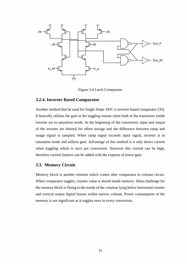
Figure 3.7 Integrator Based Ramp Generator ............................................................ 35
Figure 3.8 4-bit Synchronous Counter example using D Flip Flops ......................... 36
Figure 3.9 4-bit Asynchronous Counter example using D Flip Flops ....................... 36
Figure 4.1 Single Slope ADC Comparator Sub-Blocks ............................................. 42
Figure 4.2 Preamplifier Circuit .................................................................................. 43
Figure 4.3 Preamplifier Monte-Carlo Analysis Offset Histogram ............................. 44
Figure 4.4 Comparator Latch Stage ........................................................................... 45
Figure 4.5 Preamplifier and Latch stage output with respect to ramp signal and DC
image signal ............................................................................................................... 46
Figure 4.6 3 bit Register Circuit consisted of D-Flip-Flops....................................... 47
Figure 4.7 Ramp Generator Circuit Topology ........................................................... 48
Figure 4.8 Rail-to-Rail Folded Cascode Amplifier .................................................... 49
xvi
Figure 4.9 Operation of Ramp Generator with respect to reset and enable signal ..... 50
Figure 4.10 AC Frequency Response of Ramp Generator Integrator Amplifier ....... 51
Figure 4.11 Ramp Generator Current Source Circuit ................................................ 52
Figure 4.12 Ramp Generator linearity response with the derivative of ramp signal . 53
Figure 4.13 AC Frequency Response of the Current Source Feedback Amplifier .... 54
Figure 4.14 Ramp Generator Calibration Feedback ................................................... 55
Figure 4.15 Ramp Calibration Simulation Result after power-up ............................. 56
Figure 4.16 4-bit synchronous counter ....................................................................... 57
Figure 4.17 Settling behavior of counter outputs as received from various column
circuits from near side to far side of the counter circuit ............................................. 58
Figure 4.18 Out-of-range simulation and behavior of the memory output ................ 59
Figure 4.19 Power Down operation of the comparator after crossing of the ramp .... 60
Figure 5.1 Fabricated digital output ROIC ................................................................. 63
Figure 5.2 Single Slope ADC operation..................................................................... 64
Figure 5.3 ADC output response with respect to applied sine wave .......................... 65
Figure 5.4 128 point FFT Result of the ADC for 77 K temperature .......................... 66
Figure 5.5 128 point FFT Result of the ADC for 300 K temperature ........................ 67
Figure 5.6 Layout of 6 column ADC placed side by side .......................................... 68
Figure 5.7 Shared Circuit Layout ............................................................................... 69
Figure 5.8 Test setup consisting of cryostat, analog and digital interface board ....... 70
Figure 5.9 Integrator Amplifier’s response to the pulse signal for various input bias
currents ....................................................................................................................... 71
Figure 5.10 Ramp Generator Measured Waveform ................................................... 72
Figure 5.11 Calibration DAC Output Voltage with respect to calibration phase ...... 73
Figure 5.12 Ramp Slope change for various calibration voltages .............................. 74
Figure 5.13 ADC Digital Response with respect to integration time for various injected
detector currents ......................................................................................................... 75
Figure 5.14 ADC Output Response with respect to injected input voltage for various
ADC resolutions ......................................................................................................... 76
Figure 5.15 Measured Frequency Response .............................................................. 77
Figure 5.16 Sine wave distortion regarding input stage ............................................. 78
1
CHAPTER 1
1. INTRODUCTION
With the widespread adoption of semiconductors since the mid of past century,
semiconductor technology has found many different application areas. One prominent
area of solid state materials is imaging technology. In 1963, Morrison invented the
first image sensor [1] and other inventors followed him allowing widespread adoption
of image sensors. Since then, different types of image sensors have been developed,
which detect different bands of electromagnetic spectrum ranging from UV to THz
band nowadays.
Infrared is a form of radiation that is invisible to the human eye which extends from
0.7 µm to several tens of µm. Due to the blackbody radiation, all objects emit infrared
light according to their temperature. Hence, infrared imaging allows observing the
field of view even without visible light.
Today, infrared imaging systems are utilized in wide application areas ranging from
military surveillance to medical diagnosis. These applications include missile tracking,
night vision, surveillance, target acquisition as well as spectroscopy, weather
forecasting and medical diagnosis such as cancer detection. As semiconductor
technology keeps developing, the demand for advanced infrared imaging systems will
also increase. Technology trend pushes infrared systems to have more pixels with
smaller pitch and higher readout speeds.
In order to detect infrared photons, special detector materials for different bands are
required. Two main components of an infrared imaging system are FPA and ROIC.
The formation of detector pixels are called Focal Plane Arrays (FPAs). Infrared FPA’s
needs to be hybridized with a readout integrated circuit (ROIC) to convert infrared
detector signal into the meaningful image data.
2
1.1. Challenges and Motivation
Over the last couple decades, much attention has been granted to image sensor
development due to its commercial and strategic value. This development involves
smaller and increased number of pixels as well as lower noise level and higher dynamic
range. According to Moore’s law, the number of transistors on integrated circuits are
expected to be doubled in every 18 months. This scaling trend also benefits image
sensor development, allowing smaller pixel pitches and column circuits [2]. Smaller
pixel pitch yields smaller dies and decreases costs. However, pixel scaling trend for
the image sensors have been decelerated in recent years due to the optical diffraction
limit.
Visible image sensor development has been leading to the entire image sensor business
due to the strong market demand and competition. Most of the new features and
technologies are firstly observed for visible sensors and scientific, medical and military
applications follow those improvements. One example to this trend is the output type
of the sensor. Initially developed visible sensors adopted analog output type, whereas
market demand gradually forced CMOS image sensors to acquire digital output due to
its advantages that will be covered in the following chapters [3]. Nowadays, X-Ray
sensors, UV Tubes as well as infrared ROIC’s have adopted digital output type [4].
Digital output ROIC provides several advantages compared to its analog counterpart.
Digital output ROIC does not need any ADC proximity card, allowing simplification
of the system which is critical for military surveillance applications. Moreover, this
elimination reduces system cost associated with external ADC components. Digital
output also reduces system noise such that digital signals are resistant to environmental
coupling and perturbations caused by dewar [5]. For the analog case, non-differential
analog output is susceptible to those unfavorable effects. In terms of power,
elimination of analog line and video buffer amplifiers compensate for the additional
power consumed by ADC’s which decrease the overall power budget which is
important for cooled systems. On-chip analog to digital conversion also allows digital
correction methods such as correlated double sampling and digital offset cancellation.
The discussion above leads to the motivation of the thesis: the design of an ADC which
will be integrated into cooled ROIC to achieve digital output. A prototype ADC has
been designed with 0.18 µm CMOS technology and integrated into a ROIC with
3
proper timing and layout arrangement. ROIC has been manufactured and coupled with
LWIR detector in order to capture sample infrared images.
1.2. Design Overview
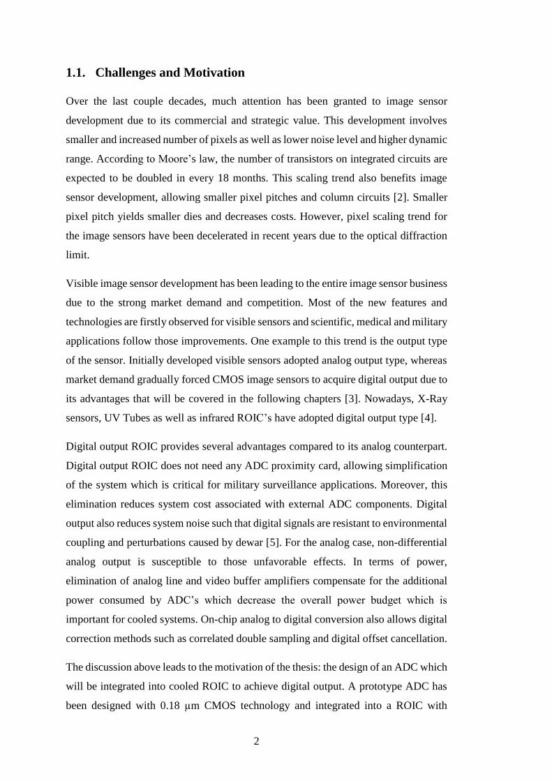
This thesis uses 0.18 µm CMOS technology for the circuit design. Figure 1.1 presents
the architecture of the ROIC. During integration duration, photo generated current is
collected inside the pixel capacitors. For the readout, signals stored in pixels are
sampled row by row by the analog variable gain amplifier. Following column parallel
ADC stage reads and digitizes sampled signals. Digitized signal values are stored by
memory elements and multiplexed column by column to the output pads.
MUXPixel ArrayGain
Amplifier ADC
Bias GeneratorTiming
Sequencer
Figure 1.1 ROIC Readout Channel
1.3. Thesis Organization
This thesis consists of 6 chapters. Chapter 2 is based on literature survey for image
sensor design principles. It begins with electromagnetic spectrum and electro-optic
principles. Then performance parameters are explained for the solid state image
sensors followed by readout circuit architectures. Finally, on-chip ADC placement
topologies and comparison of different ADC architectures are presented.
In Chapter 3, column parallel single slope ADC operation principle and different
design approaches will be presented with the design challenges.

4
In Chapter 4, provides an overview of the implantation of the ADC stage. Sub-blocks
that constitute the ADC are explained individually. Design challenges and layout
considerations are projected.
In Chapter 5, simulation and experimental results of the ADC is given. Performance
analysis as well as overall ROIC functionality with the digital output is discussed.
In Chapter 6, conclusions are drawn to summarize the contribution of the thesis and
future work is discussed.
1.4. Research Objectives and Author Contribution
The fundamental object of this thesis is to implement a single slope ADC circuit
suitable for image sensors and to successfully integrate it into a digital output Readout
Integrated Circuit (ROIC). With the implementation of the ADC circuit, the definite
goals of this research are listed as follows:
1. Analysis of the digital output ROIC with respect to its analog output
counterpart is fulfilled. The effect of implementation of ADC into ROIC is
evaluated. Advantages and disadvantages of digital output method is analyzed.
2. Analysis of ADC placement topologies within ROIC is carried out. Different
methods to position ADC circuit and their optimization for different
applications is covered. According to the placement of ADC, system
requirement analysis for ADC design is evaluated and supported with
calculations.
3. Comparison of different ADC types for image sensors are presented. Their
performance parameters and limitations are listed. Feasibility of various ADC
types and their selection criteria is conveyed.
4. Imaging system performance analysis for cooled infrared systems is explained.
Derivation and optimization of ADC resolution, considering photodiode
related limiting factors, is analyzed with the tradeoffs such as power
consumption.
5. Effects of the cryogenic environment to the CMOS circuits are evaluated.
Guidelines and design approaches are indicated with explanations.
6. The design and layout of the single slope ADC circuit is performed. Single
slope ADC is supposed to be compatible with the image sensors and its

5
resolution performance should meet system criteria. In order to be more
efficient than analog output ROICs, digital ROIC have to include a
substantially efficient ADC structure. Design approaches are presented for the
top level and block level circuits.
7. Calibration circuit for ramp generator is proposed to cancel out unfavorable
effects of cryogenic temperature and mismatch caused by CMOS fabrication
process. Operation principle of calibration and its feedback loop is bring out.
8. Integration of single slope ADC into the digital ROIC is targeted within the
scope of this research. Timing sequence is generated synchronously within
readout operation. Even distribution of required timing signals and bias
generation is handled.
9. Validation of the fabricated ADC is realized via experimental tests. Various
tests should be conducted to ensure operability.
The main contribution of the author in this thesis is implementation and integration
of the ADC circuit inside to the readout columns with proper bias and timing
controls. Design of the ADC stage includes peripheral common blocks that each
column ADC’s share alongside ADC column circuit which is responsible for
digitization operation. All the layout work regarding those blocks is carried out by
the author. On the other hand, the digital output ROIC is a cooperative work carried
out with VLSI design team of ASELSAN. There are peripheral circuits, digital
timing controllers, pixel design and output multiplexer are designed and laid out
by various members of the team. Moreover, the design of analog and digital boards
for testing ROIC are carried out by other people.

7
CHAPTER II
2. LITERATURE REVIEW
This chapter is dedicated to literature background about ROIC design and
architectures. In Section 2.1, photo detection operation is mentioned and performance
parameters of solid state image sensors are provided. Section 2.2 compares analog and
digital ROIC architectures. In Section 2.3, different ADC placement topologies are
evaluated. Section 2.4 provides information about ADC architectures that can be used
as column parallel and their comparison.
2.1. Image Sensors Background
2.1.1. Optical Absorption and Photo Detection
According to the Plank’s law, photons with an energy of E=hf where h is the Plank’s
constant and f is the frequency of the incident light, may be absorbed by the direct
bandgap semiconductor whose bandgap energy is smaller than photon’s energy. In that
case, photon interacts with an electron in a valence band and elevates the electron into
the conduction band leading to an electron hole pair. However, for the case of indirect
bandgap semiconductors, incident photons do not provide required momentum change
for the electron excitation to the conduction band.
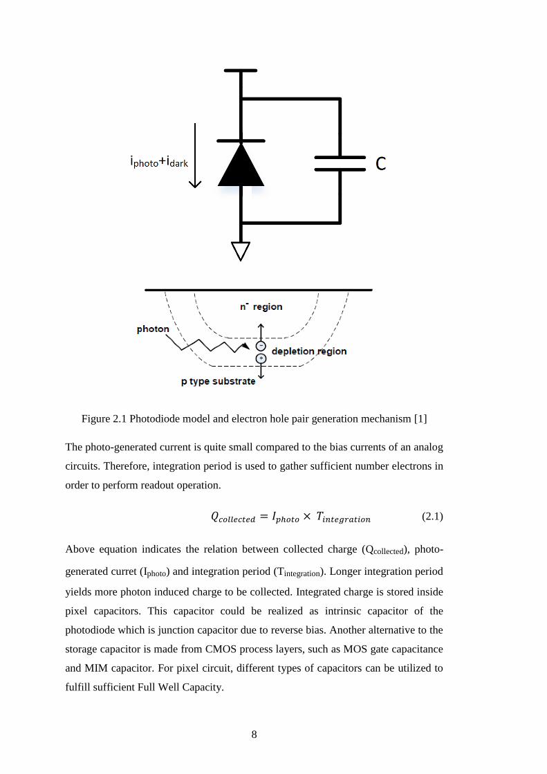
Solid state image sensors most commonly utilize photodiode as a photo detector.
Photodiode is a reverse biased p-n junction device which generates electron hole pairs
upon incident photons. In Figure 2.1, photocurrent generation is shown that absorbed
incident light creates electron hole pairs. These electron hole pairs are separated by the
electric field caused by either externally applied bias or built-in electrical potential.
The magnitude of the photo-generated current is proportional to the number of
incoming photons, which is intensity of light.
8
Figure 2.1 Photodiode model and electron hole pair generation mechanism [1]
The photo-generated current is quite small compared to the bias currents of an analog
circuits. Therefore, integration period is used to gather sufficient number electrons in
order to perform readout operation.
𝑄𝑐𝑜𝑙𝑙𝑒𝑐𝑡𝑒𝑑 = 𝐼𝑝ℎ𝑜𝑡𝑜 × 𝑇𝑖𝑛𝑡𝑒𝑔𝑟𝑎𝑡𝑖𝑜𝑛 (2.1)
Above equation indicates the relation between collected charge (Qcollected), photo-
generated curret (Iphoto) and integration period (Tintegration). Longer integration period
yields more photon induced charge to be collected. Integrated charge is stored inside
pixel capacitors. This capacitor could be realized as intrinsic capacitor of the
photodiode which is junction capacitor due to reverse bias. Another alternative to the
storage capacitor is made from CMOS process layers, such as MOS gate capacitance
and MIM capacitor. For pixel circuit, different types of capacitors can be utilized to
fulfill sufficient Full Well Capacity.

9
2.1.2. Infrared Spectrum and Infrared Detectors
Infrared light is an electromagnetic wave which has longer wavelength than visible
light. It is first discovered by William Hershel when he found out that sunlight passing
through prism also heats surface beyond red region which is invisible to the human
eye. It is ranging from 0.7 µm up to 100 µm in electromagnetic spectrum.
Infrared spectrum have been separated into sub-regions such as Near Infrared Region
(NIR) (0.7 µm-1 µm), Short Wave Infrared (SWIR) (1 µm-1.7 µm), Mid Wave
Infrared (MWIR) (3 µm-5 µm) and Long Wave Infrared (LWIR) (8 µm-12 µm).
Infrared detectors are sensitive to the specific spectrum of the infrared light. Different
types of infrared detectors according to their bandgap can be selected as infrared
detector. Typical detector materials can be listed as follows: for SWIR band, InGaAs;
for MWIR band InSb and HgCdTe; for LWIR band HgCdTe, Micro-Bolometer and
QWIP. For visible and NIR case, Silicon can be used which reduces cost for monolithic
integration. Among these materials, microbolometers are thermal detectors which
sense heat, and others are photodiode type detectors which sense infrared photons [6].
According to the Stefan-Boltzman law [7], spectral emission from the target depends
on target’s temperature. For a blackbody target, the spectral radiant exitance can be
stated as
Me(λ, T) =2πhc2
λ5(ehc
λkT⁄−1)
(2.2)
where h is the Plank’s constant, c is the speed of light, λ is the wavelength of the
photon, k is the Boltzman constant and T is the temperature of the target in Kelvin
degrees. Figure 2.2 presents the spectral exitance values of blackbody objects with
different temperatures. As temperature increases, the exitance spectrum will shift
towards lower wavelengths.

10
Figure 2.2 Blackbody spectral exitance with respect to wavelength for various
temperatures from 77K to 4000K [7]
For room temperature (300 K), blackbody radiation is centered on 8 µm-12 µm band
which is LWIR band. For that reason, human surveillance applications may utilize
LWIR band. Higher temperature objects such as missile and aircraft plume is most
effectively detected at MWIR band. SWIR band is mostly used for night vision
applications, however, active illumination such as light from other objects like sun or
moon is needed for SWIR detection. On the other hand, target objects passively emit
MWIR and LWIR infrared light due to their temperature. Therefore, LWIR and MWIR
do not need any external light source.
2.2. Readout Integrated Circuit
Readout Integrated Circuit (ROIC) is an application specific integrated circuit (ASIC)
that is responsible for converting detector currents into the meaningful video data. It
acts as an interface between focal plane array (FPA) and signal processing unit. ROIC
is responsible for integrating charges as it handles charge to voltage conversion,
amplification and multiplexing the signals through rows and columns to the video
11
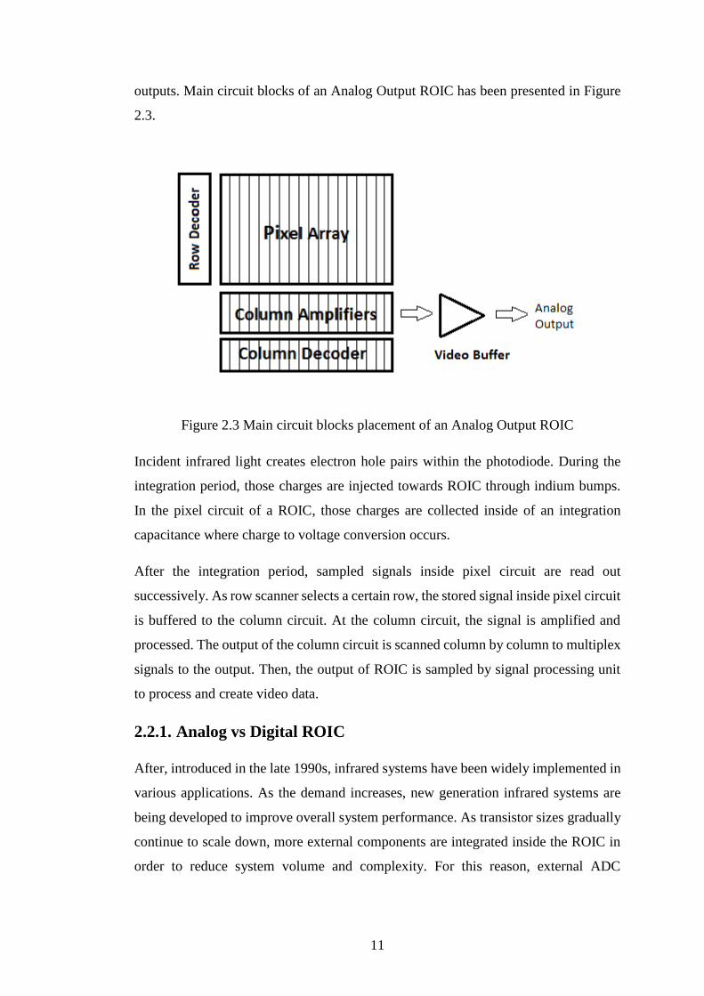
outputs. Main circuit blocks of an Analog Output ROIC has been presented in Figure
2.3.
Figure 2.3 Main circuit blocks placement of an Analog Output ROIC
Incident infrared light creates electron hole pairs within the photodiode. During the
integration period, those charges are injected towards ROIC through indium bumps.
In the pixel circuit of a ROIC, those charges are collected inside of an integration
capacitance where charge to voltage conversion occurs.
After the integration period, sampled signals inside pixel circuit are read out
successively. As row scanner selects a certain row, the stored signal inside pixel circuit
is buffered to the column circuit. At the column circuit, the signal is amplified and
processed. The output of the column circuit is scanned column by column to multiplex
signals to the output. Then, the output of ROIC is sampled by signal processing unit
to process and create video data.
2.2.1. Analog vs Digital ROIC
After, introduced in the late 1990s, infrared systems have been widely implemented in
various applications. As the demand increases, new generation infrared systems are
being developed to improve overall system performance. As transistor sizes gradually
continue to scale down, more external components are integrated inside the ROIC in
order to reduce system volume and complexity. For this reason, external ADC

12
components can be integrated inside ROIC thanks to modern sub-micron CMOS
processes.
Integrating ADC to ROIC reduces the component number in the system and has
several advantages. Firstly, considering the improvement of the CMOS process
technology, more integration yields improved system performance and reliability and
reduces associated component costs. Moreover, system volume, complexity and
required wire connections are reduced because of the removal of ADC card. This
allows implementation of more compact systems, which is critical for infrared
applications such as missile and avionics systems.
One of the advantages of digital ROIC is improved noise performance. Generally,
noise performance of a ROIC depends on the signal chain [8]. Analog output is
susceptible to Electromagnetic Interference (EMI), power supply noise and
interconnect coupling with other signals, which harms the quality of the output signal.
However, digital output is resistant to all of those effects due to its nature. Hence it
will increase signal to noise ratio of the ROIC.
Additionally, the overall power consumption of the ROIC can be reduced by the
integration of the ADC [9]. With the removal of high bandwidth video and reference
buffers, the overall system power consumption may be reduced if efficient ADC
structures are utilized.
2.2.2. Digital ROIC ADC Placement Topologies
Digital ROIC is different than from Analog ROIC such that it contains an ADC which
is responsible for converting analog image signals to the digital signal. There are
different ADC placement topologies which differs in sample frequency, resolution and
layout floorplan area [10]. For this case, layout floorplan area is very important
because most of the systems are area limited. Thus, integrated ADC layout area cannot
be as large as external ADC area. Moreover, due to limited available area, mismatches
between transistors become an important issue.
Basically, there are 3 main ADC placement topologies. These are chip level ADC,
column level ADC and pixel level ADC. Initial image sensor designs contained chip
level ADC’s, however as pixel count grows gradually, other topologies have also
gained interest. The most popular method nowadays is column level ADC which is the

13
optimum choice in terms of area and sampling speed. In the following sections, these
topologies will be examined in detail.
2.2.2.1. Chip Level ADC
Chip level ADC placement topology depends on having an ADC at the last stage of
the ROIC. Main advantage is that ADC may span relatively larger layout area
compared to the other architectures because of the fact that ADC is placed out of pixel
and column array which are limited to the pixel pitch. Hence, there is no pitch size
confinement. Due to the vast available area, this method is the simplest implementation
method in terms of layout. Chip level ADC topology is presented in Figure 2.4.
Figure 2.4 Chip Level ADC
ADC operating frequency can be stated as:
𝑓𝑠𝑎𝑚𝑝𝑙𝑖𝑛𝑔 = 𝑓𝑟𝑎𝑚𝑒 𝑝𝑒𝑟 𝑠𝑒𝑐𝑜𝑛𝑑 × 𝑐𝑜𝑙𝑢𝑚𝑛 𝑐𝑜𝑢𝑛𝑡 × 𝑟𝑜𝑤 𝑐𝑜𝑢𝑛𝑡 (2.3)
As pixel array grows, sampling speed has to be scaled accordingly. Therefore, very
high speed ADC is required for this topology. For modern image sensors which have
millions of pixels and high frame rates, this requirement is a big challenge.
Main advantage of this topology is larger available layout area. Also, pixel pitch
scaling does not affect this ADC topology because of its position outside of the pixel
and column array. Hence, complex and high resolution ADC’s which span relatively
larger area can be utilized in this topology. Another advantage is lower image non-
uniformity as whole pixel array are converted by the same ADC. In the other
14
topologies, there will be high number of ADC’s whose offsets are different from each
other.
However there are also disadvantages of this topology. Due to the high frequency
specifications of the ADC, the design will be challenging. For larger arrays,
technology process limitation does not allow design of such a high speed ADC. This
high frequency demand will also decrease ADC power efficiency, consuming higher
power per conversion. Moreover, longer analog chain before ADC, yields low SNR
level.
2.2.2.2. Column Level ADC
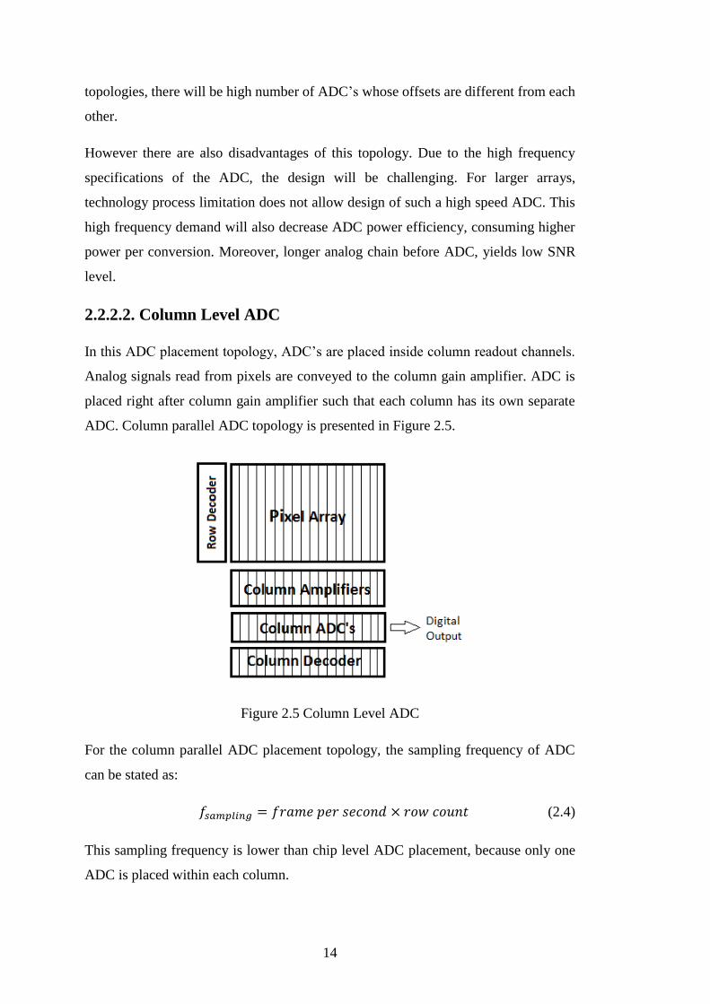
In this ADC placement topology, ADC’s are placed inside column readout channels.
Analog signals read from pixels are conveyed to the column gain amplifier. ADC is
placed right after column gain amplifier such that each column has its own separate
ADC. Column parallel ADC topology is presented in Figure 2.5.
Figure 2.5 Column Level ADC
For the column parallel ADC placement topology, the sampling frequency of ADC
can be stated as:
𝑓𝑠𝑎𝑚𝑝𝑙𝑖𝑛𝑔 = 𝑓𝑟𝑎𝑚𝑒 𝑝𝑒𝑟 𝑠𝑒𝑐𝑜𝑛𝑑 × 𝑟𝑜𝑤 𝑐𝑜𝑢𝑛𝑡 (2.4)
This sampling frequency is lower than chip level ADC placement, because only one
ADC is placed within each column.

15
Main limitation of the column parallel placement is the available layout area. ADC
layout width cannot exceed the pixel pitch. However, there is no limitation for length
of ADC. Hence, column parallel ADC layout is designed in a narrow stripe shape. It
is also possible that column readout channels can be placed at both sides of the pixel
array. In such case, ADC length is equal to the two times of pixel pitch size. There is
also some ADC examples in the literature that spans more than two columns by column
multiplexing [11].
There are also disadvantages of column parallel ADC placement. Each column ADC
has various amount of offset, which causes stripe like artifacts in the image. These
stripes are called Fixed Pattern Noise (FPN). To deal with this issue, different offset
cancellation and correlated double sampling methods are developed [12].
Column parallel ADC is the most common ADC type used in image sensor designs.
In terms of area and sampling speed, column parallel ADC placement is the optimum
choice among other topologies. For modern image sensor designs, pixel ADC is most
likely area limited due to the narrow pitches. Also, chip level ADC is sampling speed
limited due to the larger arrays. However, column parallel placement has adequate
layout area and feasible sampling speed.
2.2.2.3. Pixel Level ADC
Another digital ROIC implementation method is pixel level ADC placement method.
In this method, each pixel circuit has its own ADC. Analog to digital conversion is
conducted at the first stage of the signal chain, hence allowing lower noise levels. Also,
the number ADC’s are equal to the number of pixels, hence sampling speed is equal
to the FPS frequency [13]. Pixel level ADC topology is shown in Figure 2.6.
𝑓𝑠𝑎𝑚𝑝𝑙𝑖𝑛𝑔 = 𝑓𝑟𝑎𝑚𝑒 𝑝𝑒𝑟 𝑠𝑒𝑐𝑜𝑛𝑑 (2.5)

16
Figure 2.6 Pixel ADC
In this method, analog circuits are minimized in the whole ROIC and they are only
located inside the pixel circuit [14]. All the other circuits are digital which are resistant
to the noise and interference effects. Therefore, pixel level ADC is able to provide
highest SNR level with respect to other topologies.
However, the main drawback of the pixel level ADC is the layout area limitation. ADC
has to fit inside pixel area which is difficult to sustain recent image sensor trend of
having smaller pixel pitches [15]. Additionally, digital multiplexing and memory
circuits should be implemented inside the pixel circuit. Due to this limitation, pixel
level ADC is not common for image sensors. However academic research and
development is still ongoing for this placement type.
2.3. ADC Requirements for Image Sensors
ADC requirements for image sensors depend on readout architecture of the system,
array format and sampling speed. As mentioned in previous sections, column parallel
ADC is suitable for lower frequency operation in the expense of increased number of
ADC count. General requirements of ADC’s are applicable to the image sensor
ADC’s, although there are also specific image sensor related requirements. The
requirements and their explanations are listed below:
2.3.1. Area
For the column parallel ADC architecture, available ADC area is a challenge for
modern narrow pitch image sensors. ADC has to fit inside narrow stripe like area in
17
the column readout arrays. For this reason, placement of large area ADC designs such
as SAR ADC due to its capacitor array is compelling in terms of layout.
2.3.2. Sampling Frequency
For the column parallel ADC’s, ADC should be able to sample analog signal from the
gain amplifier and convert until next signal becomes available. This can be challenging
for high FPS and large format arrays. Due to this reason, single slope ADC cannot be
used for demanding applications.
2.3.3. Power Consumption
Power is one of the important parameters for image sensors. In order to be more
efficient than analog output ROIC’s, ADC should consume less power than analog
buffer counterparts. Also, routing power supply wires with acceptable ohmic drop
become significant issue with limited number of metal layers. To deal with this
situation, efficient ADC structures are utilized such as single slope ADC. Moreover,
low power consumption is very important for cooled infrared systems due to the
limited efficiency of cyro-cooler.
2.3.4. Effective Number of Bits (ENOB) and Signal to Noise Ratio
Due to the various noise sources, converted ADC output has a deviation from the ideal
output. The noise can be caused by ADC itself or external sources such as bias and
power supply noise. In order to perform better than analog output ROIC’s, ADC has
to satisfy system specifications such that its noise should be lower than other noise
components such as dark current and photon shot noise. ENOB is calculated as
ENOB= (SNR-1.76)/6.02 which is the most common way to define ADC performance.
2.3.5. Integral Non-Linearity (INL)
Integral Non-Linearity is described as a difference between quantized digital signal
level and the ideal value with respect to given low and high reference values of ADC.
It also contributes to the FPN value. It is a static non-linearity so that it can be
eliminated by external two-point non-uniformity correction.

18
2.3.6. Differential Non-Linearity (DNL)
Differential Non-Linearity is deviation of the output step size width with respect to the
ideal step size width. In order ADC not to miss any code, ADC should have a DNL
value less than LSB value. If this condition is satisfied, ADC is guaranteed to be
monotonic. For a sustainable performance, DNL should meet the criteria of DNL < 0.5
LSB. Larger DNL values yields loss of discrete image sub-levels, lowering ADC’s
ENOB level, therefore reduction of the image quality. DNL is more important than
INL, because DNL errors cause image artifacts and they can be easily detected by eye.
2.3.7. Fixed Pattern Noise (FPN)
Non-linearity and offset between column ADC’s appear as vertical stripe artifacts in
the resultant image. The main problem is caused by correlation of error throughout
channel. Human visual perception is more sensitive to the FPN than random pixel
noise because of its spatial correlation [16]. For chip level ADC placement,
nonlinearity effects are same for all pixels whereas pixel level ADC causes random
noise distributed across pixel array, hence no correlation exists between columns.
Therefore, FPN is problematic only for column parallel ADC’s. In order to reduce FPN
level, offset cancellation or correlated double sampling can be applied. Correlated
double sampling (CDS) is performed as subtracting image signal level from the reset
level. Therefore, offset and low frequency noise can be removed from the signal chain,
causing lower FPN value.
2.3.8. Out-of-Range Recovery
Image sensor ADCs have to cover all the voltage swing range in order to convert image
signal. For very bright conditions, excessive light is absorbed such that input voltage
may be outside of ADC input voltage swing range. For this case, ADC cannot
successfully convert resultant image especially for single slope ADC. To deal with this
issue, out-of-range recovery circuit has to be added to the ADC.
2.4. ADC Architectures for Column Parallel ADC
Several ADC methods can be used as column parallel ADC because of the demanding
specifications such as area and power [17]. Other methods such as Pipeline or Flash
ADC are not common for column parallel placement due to their relatively larger

19
layout footprint and higher power consumption. Due to parallelism of the ADC’s,
sampling speed is around 10 KHz to 1 Mhz in the literature. Resolution requirement
is generally around 10-14 bit range for mainstream applications. Most commonly used
architectures are Ramp ADC, SAR ADC, Sigma Delta ADC and Cyclic ADC [18].
Brief information about them is provided below.
2.4.1. Ramp ADC
Ramp ADC is the simplest and most commonly used ADC architecture for image
sensors [19]. The operation principle depends on comparison of analog sampled input
signal to on-chip generated ramp with each clock pulse. For each clock pulse, counter
circuit is incremented concurrent with rising ramp. When ramp signal crosses sampled
input signal, comparator is triggered and counter value is latched to the memory. It is
also called as Single Slope ADC if single ramp is used. The architecture of the single
slope ADC and its peripheral blocks are presented in Figure 2.7.
Figure 2.7 Main blocks of a Single Slope ADC [10]
Single Slope ADC consists of comparator, memory element, ramp generator and
digital counter. Of these circuit blocks, comparator and memory element are placed in
every column whereas ramp generator and digital counter are shared by all the
columns. Column circuit is relatively simple and area footprint is lower than other
architectures.
20
Conversion speed is the main limitation of this architecture. Required clock frequency
can be given as:
𝑓𝑐𝑙𝑜𝑐𝑘 = 2𝑛 × 𝑓𝑠𝑎𝑚𝑝𝑙𝑖𝑛𝑔 (2.6)
where n represent resolution of the ADC. It requires a many periods for conversion
operation. Hence this architecture is not suitable for high resolution and high speed
applications. However, single slope ADC is suitable for most image sensor
applications with 10-12 bit resolution and conversion speed lower than 100 Ksample/s.
In order to overcome speed limitation of the Single Slope ADC, several methods based
on ramp modification such as Multi Ramp ADC [20], Two-Step Ramp [21-22], Dual
Slope ADC [8] are also present in the literature.
Main advantages of this architecture are simplicity and low area footprint. Ramp
generator and digital counter are shared with all column ADCs, hence ADC offers low
power consumption. As ramp signal is shared with comparators, any non-linearity
effect related to ramp generator also affect all column ADC’s. Therefore non-linearity
between columns is relatively low.
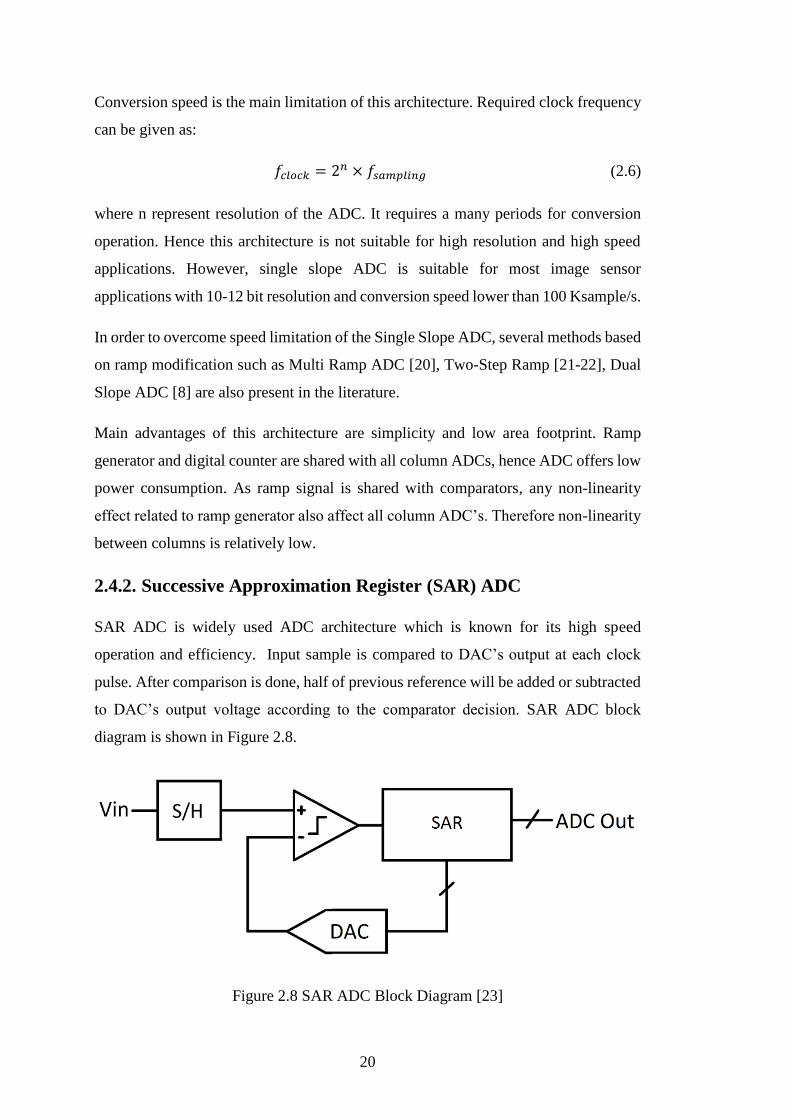
2.4.2. Successive Approximation Register (SAR) ADC
SAR ADC is widely used ADC architecture which is known for its high speed
operation and efficiency. Input sample is compared to DAC’s output at each clock
pulse. After comparison is done, half of previous reference will be added or subtracted
to DAC’s output voltage according to the comparator decision. SAR ADC block
diagram is shown in Figure 2.8.
Figure 2.8 SAR ADC Block Diagram [23]
21
SAR ADC consisted of comparator, DAC and Register block. Among these circuits,
DAC covers most of the area. Due to the process related mismatch, DAC circuit should
be designed with sufficiently large capacitors to satisfy resolution criteria. Conversion
time is faster such that only N clocks are required for N bit resolution whereas 2N
conversion is required for single slope ADC. Therefore, SAR is a relatively power
efficient ADC.
Low power consumption of SAR ADC is an important feature for ROIC design [11].
Due to the limited pixel pitch, available column width is prohibitively narrow for an
effective DAC design. Due to this reason, SAR ADC is not as common as single slope
ADC for narrow pitch circuits. However, for demanding applications with very high
sampling frequency, SAR ADC is successfully implemented as a column parallel ADC
[24-26]
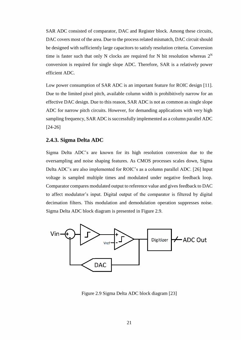
2.4.3. Sigma Delta ADC
Sigma Delta ADC’s are known for its high resolution conversion due to the
oversampling and noise shaping features. As CMOS processes scales down, Sigma
Delta ADC’s are also implemented for ROIC’s as a column parallel ADC. [26] Input
voltage is sampled multiple times and modulated under negative feedback loop.
Comparator compares modulated output to reference value and gives feedback to DAC
to affect modulator’s input. Digital output of the comparator is filtered by digital
decimation filters. This modulation and demodulation operation suppresses noise.
Sigma Delta ADC block diagram is presented in Figure 2.9.
Figure 2.9 Sigma Delta ADC block diagram [23]

22
Sigma Delta ADC has an integrator, decimator, comparator and DAC. Of these circuit
components, integrator draws significant amount of power in order to achieve required
SNR value. Sigma Delta ADC has relatively high power consumption, however there
is a progress in order to reduce overall power consumption [27-30]
2.4.4. Cyclic ADC
Cyclic (Algorithmic) ADC is preferred by its high frequency operation, however it
suffers from high power consumption [31]. Due to the area limitation of SAR ADC,
DAC is replaced with Cyclic ADC [32-33]. Instead of using DAC, input signal is
multiplied by two after being subtracted to reference value or zero according to the
comparator output. Hence, SAR like comparison is achieved with each clock pulse and
it takes N cycles to convert into N bit digital output. Cyclic ADC architecture and its
sub-blocks are displayed in Figure 2.10.
Figure 2.10 Cyclic ADC block diagram [34]
Cyclic ADC has lower area than SAR, but it consumes more power due to its low noise
amplifier. It is mainly used for high speed applications where Single Slope ADC is
insufficient in terms of speed and where SAR ADC cannot fit inside column pitch due
to the narrow pixel pitch.
2.4.5. ADC Architectures Comparison
In the previous sections, different ADC architectures are discussed and their operation
principles are covered. ADC’s architectures differ from each other by several
performance parameters such as sampling speed, resolution, layout area and power
consumption [9]. In Table 2.1 comparison of ADC architectures is given.
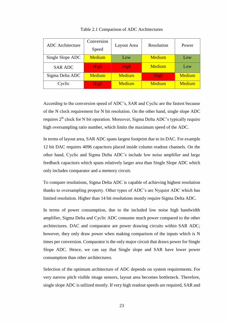
23
Table 2.1 Comparison of ADC Architectures
ADC Architecture Conversion
Speed Layout Area Resolution Power
Single Slope ADC Medium Low Medium Low
SAR ADC High High Medium Low
Sigma Delta ADC Medium Medium High Medium
Cyclic High Medium Medium Medium
According to the conversion speed of ADC’s, SAR and Cyclic are the fastest because
of the N clock requirement for N bit resolution. On the other hand, single slope ADC
requires 2N clock for N bit operation. Moreover, Sigma Delta ADC’s typically require
high oversampling ratio number, which limits the maximum speed of the ADC.
In terms of layout area, SAR ADC spans largest footprint due to its DAC. For example
12 bit DAC requires 4096 capacitors placed inside column readout channels. On the
other hand, Cyclic and Sigma Delta ADC’s include low noise amplifier and large
feedback capacitors which spans relatively larger area than Single Slope ADC which
only includes comparator and a memory circuit.
To compare resolutions, Sigma Delta ADC is capable of achieving highest resolution
thanks to oversampling property. Other types of ADC’s are Nyquist ADC which has
limited resolution. Higher than 14 bit resolutions mostly require Sigma Delta ADC.
In terms of power consumption, due to the included low noise high bandwidth
amplifier, Sigma Delta and Cyclic ADC consume much power compared to the other
architectures. DAC and comparator are power drawing circuits within SAR ADC;
however, they only draw power when making comparison of the inputs which is N
times per conversion. Comparator is the only major circuit that draws power for Single
Slope ADC. Hence, we can say that Single slope and SAR have lower power
consumption than other architectures.
Selection of the optimum architecture of ADC depends on system requirements. For
very narrow pitch visible image sensors, layout area becomes bottleneck. Therefore,
single slope ADC is utilized mostly. If very high readout speeds are required, SAR and
24
Cyclic ADC are the architecture of choice. Cyclic ADC requires higher power whereas
SAR ADC is layout limited. Sigma Delta ADC is best for its high resolution
applications but it requires much power and higher conversion speeds are not possible
due to oversampling requirement.
For digital output ROIC implementation, our system requirements enforce low power
operation which disqualifies Sigma Delta and Cyclic ADC. SAR ADC is also a good
candidate for its high frequency operation but layout area is prohibitive within our
CMOS process matching parameters in order to obtain good INL and DNL values.
Single Slope ADC is chosen for its low power and smaller layout property. Usage of
only single ramp eliminates any possible INL and DNL effect among column ADCs.
However, single slope ADC is limited by conversion speed as it requires 2N clock
period for N bit resolution which means that every bit of resolution increase halves
conversion frequency. It is still possible to achieve 14 bit resolution with
compromising sampling speed.
2.5. Infrared Imaging System Performance Analysis
Infrared imaging performance depends on many factors such as detector noise, dark
current, readout noise and ADC quantization noise. In order to define system
performance, signal to noise ratio and dynamic range is utilized. Signal to noise ratio
is defined as ratio of the total number of collected electrons to the total input referred
noise. Dynamic range is defined as maximum signal swing to the minimum resolvable
signal level which equals to the noise level.
One of the most dominant noise sources is shot noise whose value is calculated as
square root of the full well capacity (FWC). For typical MWIR and LWIR readout
circuits, 9 million electrons of full well capacity is assumed. Also analog to digital
converters introduce a quantization noise which limits the dynamic range of the ADC
where N is the bit resolution of the ADC.
There are also many other noise sources affecting imaging system analysis. Examples
to those noises are dark noise, thermal noise, 1/f noise and random telegraph signal
noise. For the system limitation analysis, only the major contributors are taken into
consideration. Hence other noises are taken as ideal for below calculations.
𝐴𝐷𝐶 𝐷𝑦𝑛𝑎𝑚𝑖𝑐 𝑅𝑎𝑛𝑔𝑒 = 6.02 × 𝑁 + 1.76 [23] (2.7)

25
𝑆ℎ𝑜𝑡 𝑁𝑜𝑖𝑠𝑒 = √𝐹𝑢𝑙𝑙 𝑊𝑒𝑙𝑙 𝐶𝑎𝑝𝑎𝑐𝑖𝑡𝑦 [17] (2.8)
𝑇𝑜𝑡𝑎𝑙 𝑁𝑜𝑖𝑠𝑒 = √𝑄𝑢𝑎𝑛𝑡𝑖𝑧𝑎𝑡𝑖𝑜𝑛 𝑁𝑜𝑖𝑠𝑒2 + 𝑆ℎ𝑜𝑡 𝑁𝑜𝑖𝑠𝑒2 (2.9)
In Table 2.2, the effect of different ADC resolutions to the calculated system
performance is presented.
Table 2.2 Infrared System Performance comparison with respect to various ADC
resolutions
ADC quantization noise and shot noise is considered as major noise sources for above
analysis. Total noise is calculated as squared sums of those two noise sources. It can
be observed that ADC quantization noise is the dominant factor for lower than 12 bit
resolutions whereas shot noise is the bottleneck for resolutions higher than 12 bit. Also,
it is worth considering that higher resolution ADC causes more power consumption.
Therefore, tradeoff between performance and power consumption is should be done
carefully. Increasing the resolution from 12 bit to 13 bit provides 1 dB extra gain but
leads to almost two times more power consumption for single slope ADC. Improving
resolution by 1 bit means that required conversion period is doubled since conversion
period of the single slope ADC depends on resolution such that 2N clock period is
required per conversion. Therefore, power consumption per conversion is increased
accordingly. After system optimization, 12 bit is found as the optimum solution for
both system performance and power consumption. Hence, Single Slope ADC for
digital ROIC is implemented with 12 bit resolution in this thesis.
ADC Resolution
ADC Dynamic
Range (db)
FWC (e-)
Quantization Noise (e-)
Shot Noise (e-)
Total Noise (e-)
S/N Ratio
System Dynamic
Range (dB)
10 61.96 9 M 7182 3000 7783.3 1156.3 61.26
11 67.98 9 M 3591.2 3000 4679.4 1923.3 65.68
12 74 9 M 1795.7 3000 3496.4 2574.1 68.21
13 80.02 9 M 897.9 3000 3131.5 2874 69.17
14 86.04 9 M 449 3000 3033.4 2967 69.45
15 92.06 9 M 224.5 3000 3008.4 2991.6 69.52

26
12 bit single slope ADC limits the system performance to the 68.21 dB. It is also
possible to increase resolution with the power consumption tradeoff. Typically, single
slope ADC’s consume two times more power for each bit of resolution increase.
27
CHAPTER III
3. SINGLE SLOPE ADC
Digital output ROIC can be done by several ADC placement topologies such as chip
level ADC, column parallel ADC and pixel level ADC as mentioned in the previous
section. Various ADC architectures are applicable and optimum ADC type differs for
each topology. Column parallel approach is found to be our architecture or choice in
terms of its optimum area footprint and speed. For column parallel topology, our ADC
requirements are 25 Ksamples per second, 12 bit resolution and lower than 40 µW
power consumption in order to give similar performance to the analog output
counterparts.
Single Slope ADC is selected over other ADC architectures for digital output ROIC.
Main advantages of single slope ADC are small layout footprint area, simple column
circuit and power efficiency due to shared structure of counter and ramp generator
circuit.
In this section, operation principles of Single Slope ADC and different design
approaches for sub-circuits are covered. Various types of circuits are can be used for
each sub-block, therefore their advantages and disadvantages are evaluated in order to
approach optimum design.
3.1. Single Slope ADC Operation
Single Slope ADC converts by comparing sampled analog input signal to the rising or
falling ramp generator concurrent with counter circuit which increments with each
clock pulse. When input signal crosses ramp signal, comparator circuit is triggered and
counter value is registered to the memory circuit [35]. By that way, analog to digital
conversion is completed. Important signals are shown in Figure 3.1.

28
Figure 3.1 Single Slope ADC Operation Principle
Single Slope ADC is consists of four main circuit elements. We can divide these
circuits into two category, column circuit and common circuit. Column circuit has
comparator and memory and these are repeated throughout columns. Common circuit
consists of counter and ramp generator and these are shared with all ADC’s together.
Due to this sharing, common circuit’s power consumption is divided into number of
columns for calculation of single ADC power consumption. Figure 3.2 shows the block
diagram of single slope ADC and its sub-blocks.
Figure 3.2 Single Slope ADC shared and column circuit blocks placement
29
3.2. Comparator Circuit
Comparator is the main conversion circuit of the Single Slope ADC. The performance
of the comparator directly affects ADC performance. It compares ramp signal and
image signal, toggles if ramp signal exceeds input signal.
Main criteria of the comparator circuit for this thesis are noise, power consumption,
kickback, bandwidth, delay time and offset. Low noise operation is essential since it
determines the resolution performance of the ADC. Power consumption of comparator
has to be low in order to keep power consumption lower than analog output ROIC’s.
Kickback effect is a noise that comparator creates when it toggles affecting previous
circuits in the signal readout channel. This issue is very important to consider since
kickback noise impacts neighboring column ADC’s due to the shared ramp signal.
Bandwidth of the comparator limits the maximum allowed speed of conversion. Low
bandwidth comparator induces delay in output toggling, which can cause nonlinearity
and missing of some bits. Offset in ADC is one of the sources of FPN which causes
vertical irregularities in the image. Therefore, comparator offset has to be low.
There are different design approaches to design a comparator analyzed in the following
sections.
3.2.1. High Gain Amplifier
Analog high gain operational amplifier can be utilized as a comparator as it saturates
the output even for smaller differential changes in the input due to the high DC gain.
They are effective for low noise operation. However, operational amplifier suffers
from limited bandwidth and high power consumption. To achieve higher bandwidth,
more current has to be drawn, which makes them unfavorable for single slope ADC’s.
3.2.2. Cascaded Gain Stages
Cascaded gain stages can be used as comparator. High bandwidth, simple one stage
amplifiers are used for this purpose [10, 36]. Last stage can be single ended for higher
gain whereas other stages have to be differential. Each stage amplifies the difference
between inputs with a certain gain, reaching sufficient gain at the final stage. However
offset should be taken into consideration because each stage amplifies previous offsets.
30
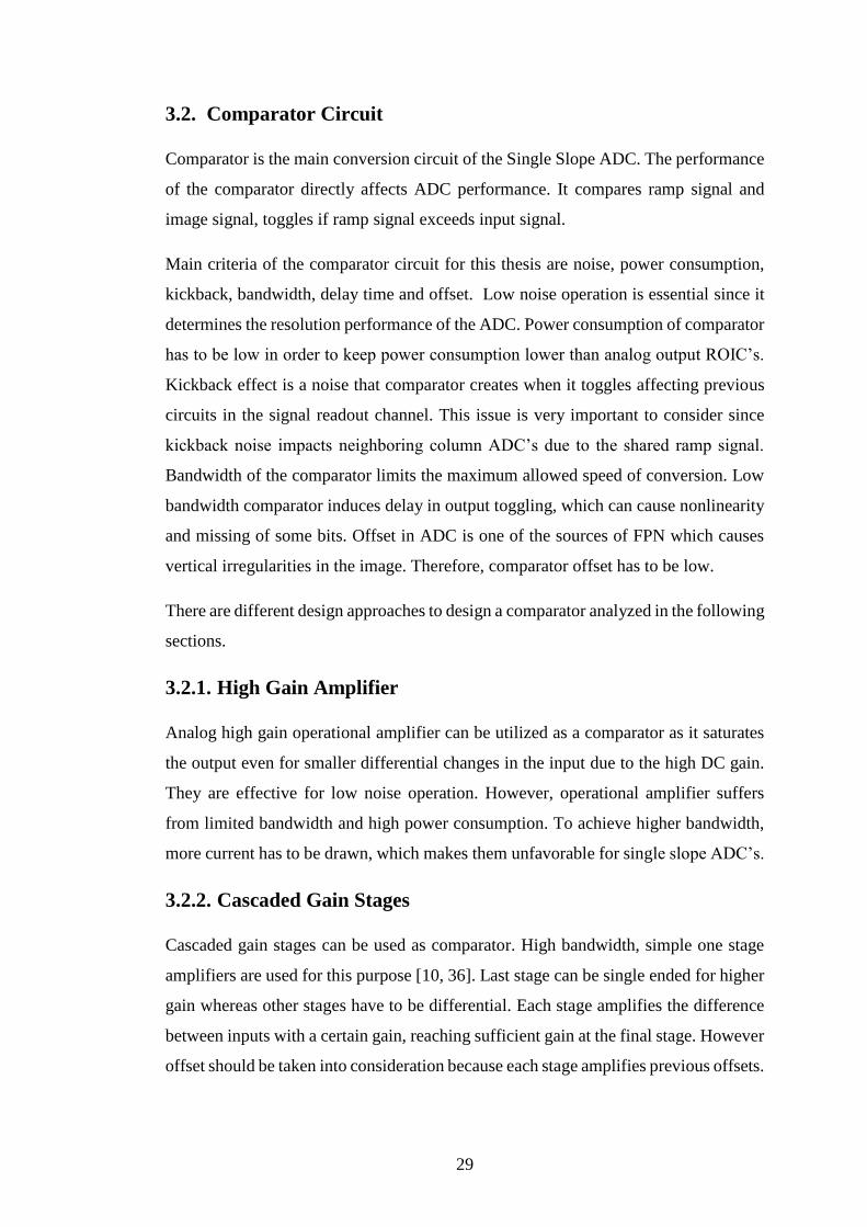
To deal with this situation, offset cancellation methods such as auto zero or correlated
double sampling can be used. 3 stage cascaded amplifier is demonstrated in Figure 3.3.
Figure 3.3 Cascaded Gain Stages
3.2.3. Clocked Comparator
Clocked (latched) comparators are one of the mostly used comparators for the ADC’s.
They consist of cross coupled inverters [37]. When clock pulse is low, both inverters
are set to high value. At the rising edge of the clock, inverters are being pulled down
by the current through input transistors which are in linear mode. According to the
input values, one side is pulled down faster than another and output is toggled. SR
latch is added to track crossings which are important for single slope operation.
This method is good for its fast settling and low power consumption. However,
dynamic and static offset [38-39], limited resolution and kickback is an issue for this
circuit. Solution to these problems is adding a preamplifier which is common for
clocked comparators. Preamplifier amplifies the difference between input signals,
which contributes resolution of the latch. Also, input referred kickback and offset are
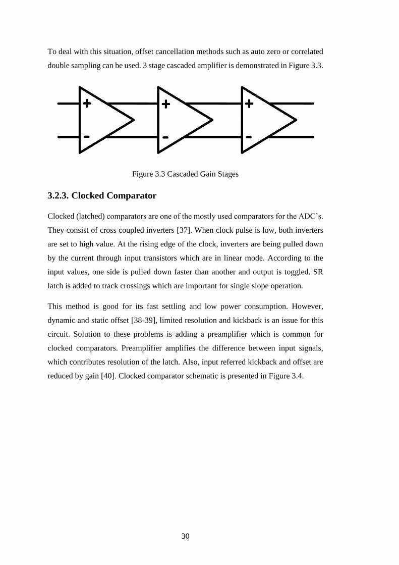
reduced by gain [40]. Clocked comparator schematic is presented in Figure 3.4.
31
Figure 3.4 Latch Comparator
3.2.4. Inverter Based Comparator
Another method that be used for Single Slope ADC is inverter based comparator [30].
It basically utilizes the gain at the toggling instant when both of the transistors inside
inverter are in saturation mode. At the beginning of the conversion, input and output
of the inverter are shorted for offset storage and the difference between ramp and
image signal is sampled. When ramp signal exceeds input signal, inverter is in
saturation mode and utilizes gain. Advantage of this method is it only draws current
when toggling which is once per conversion. However this current can be high,
therefore current limiters can be added with the expense of lower gain.
3.3. Memory Circuit
Memory block is another element which comes after comparator in column circuit.
When comparator toggles, counter value is stored inside memory. Main challenge for
the memory block is fitting to the inside of the columns lying below horizontal counter
and vertical output digital busses within narrow column. Power consumption of the
memory is not significant as it toggles once in every conversion.

32
Figure 3.5 D Flip Flop based memory circuit
There are two possible alternatives for memory block. Simplest choice is Register
made from D Flip Flop for which standard cell libraries are provided from foundry.
Design and verification are relatively easy and robust. However registers are
unfavorable in terms of layout footprint. DFF based memory is presented in Figure
3.5.
For very narrow pitch applications such as visible image sensors, SRAM is also
utilized in the industry. However, design can be cumbersome and requires expertise.
3.4. Ramp Generator
Ramp generator circuit is placed only once in the ROIC whereas such that it serves
every column. The ramp quality affects ADC performance directly; hence ramp
generator should be designed carefully. Non-linearity effects such as INL and DNL

33
could be caused by ramp generator which significantly reduces performance of the
ROIC. Monotonicity of the ramp is important in order not to miss any code.
Ramp generator has to cover swing range of the sample and hold stage. If ramp does
not cross sampled image signal, comparator will not toggle hence conversion is
unsuccessful. Due to this reason, low and high reference voltages are designed to be
programmable in order to allow margin.
There are several ramp generator architectures that can be applied to single slope ADC
for image sensors [41].
3.4.1. DAC Based Ramp Generator
Generation of ramp signal is possible to be implemented as digital to analog converter
(DAC) [42]. As counter increments at every clock pulse, output value of the counter
is fed to DAC to create corresponding analog value for given digital signal. By that
way, correlation between counter and ramp generator is done automatically. For an
ideal DAC, initial and final values of the ramp can be exactly known by reference
voltages. However, capacitive DAC’s provide less swing than reference differences
due to parasitic capacitances due to interconnects.
Ramp signal of the single slope ADC is gradually rises after conversion begins such
that only one LSB is incremented for each clock. This means that output of the DAC
always rises except for reset condition. Hence, DAC design is simpler to design as
there are no worst case conditions and response is known. DAC based ramp generator
is shown in Figure 3.6.
Figure 3.6 DAC Based Ramp Generator
Commonly used DAC unit cell types are capacitive, resistive and MOS based current
mirrors. These unit cell types are optimized for different specifications. For high speed
DAC applications, current mirrors are good candidate whereas resistive unit cells tend

34
to have slow bandwidth. In order to have good non-linearity response from DAC,
mismatch between unit cells has to be well considered so that unit cells with larger
area yields better matching. One advantage of the ramp generator circuit can be stated
as layout area outside column array is relatively large. Therefore, DAC designs with
good matching and nonlinearity response is possible to implement.
Architecture of the DAC can be implemented as unit-element DAC and binary-
weighted DAC. For single slope ADC operation, it is known that only one unit cell is
changed with each clock, hence unit-element architecture is more efficient and yields
better DNL response and monotonicity [43]. Binary weighted approach is challenging,
because incrementing from “0111…” state to “1000…” state basically require toggling
of all capacitors. Hence achieving good DNL response and monotonicity especially
for MSB bit is hard to maintain.
3.4.2. Integrator Based Ramp Generator
Integrators are widely utilized for the triangular and sawtooth generators [44]. Fixed
amount of current is fed into the integrator circuit; hence output of the integrator is
rising with certain slope. Integrator based ramp generator yields continuous ramp
signal whereas DAC based approach yields discrete ramp with a staircase pattern. The
slope of the ramp depends on current and capacitance value according to the equation
below [36]:
𝑑𝑉
𝑑𝑡=
𝑖
𝐶 (3.1)
Bigger capacitance and more current value yields better noise performance at the
integrator circuit. Also, bandwidth and noise performance of the Opamp should be
well considered such that it drives significant amount of load capacitance from column
ADC array. Integrator based ramp generator is illustrated in Figure 3.7.
35
Figure 3.7 Integrator Based Ramp Generator
During reset duration, integrator is kept at low reference voltage. When conversion
begins, current is fed to the integrator causing ramp to rise. However, the biggest
challenge for this approach is maintaining correlation between counter and ramp
generator because there is no feedback to ramp generator from counter. Therefore,
peak voltage of ramp is prone to process and mismatch variations. In the next section,
slope calibration circuit for integrator is analyzed in detail.
3.5. Counter Circuit
Counter circuit is responsible for feeding digital data to memory circuit in order to be
captured as comparator toggles. Counter circuit is relatively straightforward and easier
to implement compared to other circuits in the ADC. There are two approaches for
counter implementation of Single Slope ADC.
3.5.1. Shared Synchronous Counter
First approach is placement of only one counter whose output is shared with all column
ADC’s. Since power consumption of the counter is divided to number of columns for
power per ADC calculation, a generic synchronous counter can be utilized [45]. Digital
count data have to buffered strongly since load is high due to the sharing between
column ADC’s. Synchronous operation is essential, since counter operates at high

36
speed clock and digital output bits have to be settled at the same time before toggling
of the comparator. Synchronous counter circuit is presented in Figure 3.8.
Figure 3.8 4-bit Synchronous Counter example using D Flip Flops
It is possible to reduce power consumption by using grey code instead of binary code,
since only one bit toggles at each clock with grey code whereas for binary code almost
two bits toggle in average throughout conversion.
3.5.2. Local Asynchronous Counter
Another approach is ripple counters placed beneath each column comparator [46]. The
reason for this implementation can be stated as shared counter circuit sometimes
becomes unable to buffer its output with proper settling. This may be caused by high
speed clock frequency and high load due to large number of columns. For that case,
instead of sharing counters, a counter circuit is placed at every column. However,
overall power consumption is negatively affected. Hence, low power and area efficient
ripple counters are utilized. Output of the counter only sampled once at the end of
conversion, hence asynchronous operation is applicable. Ripple counter schematic is
projected in Figure 3.9.
Figure 3.9 4-bit Asynchronous Counter example using D Flip Flops
Ripple counter’s enable signal is controlled by comparator output. When ramp signal
is lower than image signal, counter increments with each clock pulse. After ramp

37
signal crosses image signal, counter stays same. At the end of the conversion, counter
data is conveyed to the memory for multiplexing.
Ripple counter method is capable of sustaining higher clock speeds than shared counter
method. However, power consumption is relatively higher and layout area footprint is
larger. To optimize these challenges, hybrid structure that employs both types of
counters utilizes power efficiency of shared synchronous counter and high speed
capability ripple counter [47].
3.6. Design Methodology for Single Slope ADC
In the previous sections, different approaches for Single Slope ADC are evaluated for
each sub-circuit within Single Slope ADC. In order to implement optimum ADC
which meets our system requirements, one of the design methodologies are adopted
for each sub-circuit design. In this section, trade-offs made during design phase are
evaluated.
For the design of the comparator, high speed and high resolution comparator is needed
for over 100 MHz of operation. High gain operational amplifier (>80 dB gain) and
cascaded gain stage (3 stage) approaches cannot meet high speed requirement (>100
MHz) within our system specifications in terms of power consumption (<40 µW).
Inverter based approach is prone to power supply noise due to non-differential input.
Hence clock based latch comparator approach is adopted. Latch comparator is
advantageous for its low power consumption. However, latch comparator resolution is
limited due to meta-stability region for sub-millivolt differential inputs. In order to
increase resolution, two stage preamplifier is used for additional gain.
Ramp generator block is implemented with integrator based approach. Utilizing DAC
as a ramp generator leads to a tradeoff between speed and power. Fast settling DAC’s
consume high power. Also, matching between unit cells is a cumbersome issue for
high resolution DAC’s due to process limitation. On the other hand, integrator based
ramp generator block spans relatively small area and power efficient. However,
determining ramp swing range within absolute voltage references is a design challenge
due to process and mismatch variation issues especially for cryogenic temperatures at
which transistor parameters are affected significantly. For that reason, calibration
feedback circuit is implemented to overcome this challenge.

38
For the memory block, D Flip Flop based registers are used due to their simplicity. 15
µm pixel pitch allows placement of flip flops in columns. For further pixel scaling
down, flip flops are impossible to be implemented within column pitch. Thus, SRAM
is implemented for very narrow pitch devices, however this requires a special
expertise. For our system case, flip flops are chosen for their simplicity and robustness.
Counter implementation is realized as synchronous counter whose output is shared by
all columns. Ripple counters can provide lower power consumption but causes delay.
As counter’s outputs are shared by all columns, power consumption is dominated by
load, hence power consumption of counter is negligible. In our case, synchronicity is
far more important such that all columns receive properly settled counter signals.

39
CHAPTER IV
4. IMPLEMENTATION
In this section, author’s implementation of single slope ADC is presented in the light
of the architectures covered in previous section. According to the specifications, ADC
design has been optimized in order to make digital output ROIC competitive to analog
output ROIC in terms of performance requirements. In Section 4.1, signal chain
overview is mentioned. Section 4.2 presents cryogenic design guidelines. Section 4.3
covers ADC architecture and specifications. Section 4.4 to 4.8 present design and
simulation of comparator, memory, ramp generator, counter and out-of-range recovery
circuit successively.
4.1. Overview
In digital output ROIC implementation, charges collected at the pixel is converted into
voltage signal. Upon selection of the row, image signal is buffered by amplifiers inside
pixel to the gain amplifier located in column readout channels. Image signal is
amplified and conveyed to the sample and hold stage. ADC takes sampled image signal
and converts it into digital data which is multiplexed to the pads afterwards.
In this thesis, author has fulfilled implementation and integration of the Single Slope
ADC into the digital ROIC.
4.2. Cryogenic Design Guidelines
Cooled Infrared Detectors operate at cryogenic temperatures (77 K) in order to
suppress dark current caused by narrow bandgap semiconductor. Therefore, ROIC’s
will also operate at cryogenic temperatures. Special measures have to be taken to
ensure operability for all the chips.

40
Cryogenic systems require a cooling system to be operated at cryogenic temperatures.
Due to very low efficiency of coolers at those temperatures, most of the power is
consumed by coolers to compensate heat load caused by power consumption of the
ROIC inside the Dewar. Therefore, all the circuits should be designed carefully in
order to achieve low power consumption.
Current mainstream CMOS foundries provide transistor parameters according to their
characterization. These models are valid for wide range of temperatures from 85
degree to -40 degree Celsius. However, using those transistor models at a temperature
outside this range may cause unfavorable effects and simulation results does not reflect
the real condition. Electronic Design and Automation (EDA) tools extrapolate valid
transistor parameters into cryogenic region for simulation purposes in order to give an
insight to designer but those results should be evaluated carefully.
In order to design a chip for cryogenic temperature, the effects of cooling down are
taken into consideration. Main effects are listed below:
Higher threshold values
Higher transconductance values
Lower leakage
Lower thermal noise
Due to the higher threshold value, transistors’ headroom is reduced and amplifier
swings are narrowed down. Additionally, actively biased transistors might be turned
off due to high threshold value. Hence, all active bias drivers are made programmable
through computer memory interface in order to take action against any unexpected
temperature effect.
Higher transconductance value yields higher gain for analog amplifiers. For low power
operation, transistors are biased near subthreshold region for optimum design.
However, these transistors might fall into the subthreshold region changing the
operation mode and might cause unfavorable effects. To overcome this issue, all
current bias values are made programmable as well. With the help of this feature,
optimum bias values can be found by trial and error method.
Lower operating temperatures yields lower thermal generation of charges, therefore,
leakage and dark current effects are reduced. Additionally, thermal noise is reduced

41
significantly at cryogenic temperatures. Thermal noise equation for the MOS
transistors can be stated as:
𝑉𝑡ℎ𝑒𝑟𝑚𝑎𝑙_𝑛𝑜𝑖𝑠𝑒 ̅̅ ̅̅ ̅̅ ̅̅ ̅̅ ̅̅ ̅̅ ̅̅ ̅̅ = √(8
3) × 𝑘 × 𝑇 × 𝑔𝑚 (3.1)
where k is Boltzmann constant, T is temperature and C is capacitance. For comparison,
circuits at 77 K have half of the noise level of their counterparts at 300 K. Increase in
transconductance value will additionally reduce overall noise.
4.3. Single Slope ADC Requirements
Main requirement of this project is to implement a digital output ROIC by integrating
Single Slope ADC. Therefore, it should meet the performance criteria for the analog
output ROIC’s. According to these criteria, ADC specifications are listed in Table 4.1.
Table 4.1 ADC Specifications
Specification Target Unit Comment
Resolution 12 Bit 10 to 12 bit programmable
Input Clock 120 MHz
Input Swing Range 0.75- 2.55 V
Power Consumption < 60 µW
Power Supply 1.8 & 3.3 V Digital and Analog Supply are
separated.
Temperature -200 ℃ Cryogenic temperature
Sampling Frequency 100 KHz For 10 bit operation
In order to optimize ADC operation, fast and slow operation modes are implemented.
Unfavorable feature of single slope ADC is high speed limitation such that takes 2N
clock cycles per conversion. Hence 1024 clock period is required for 10 bit operation
and 4096 clocks are required for 12 bit operation. User is allowed to program ADC
operation according to their system specification. This programmability is done by
changing counter’s max count range and current source multiplier in the ramp
generator block to increase ramp slope. Other circuit blocks are remained same.
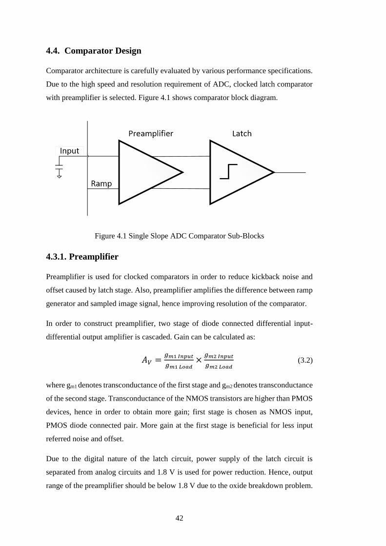
42
4.4. Comparator Design
Comparator architecture is carefully evaluated by various performance specifications.
Due to the high speed and resolution requirement of ADC, clocked latch comparator
with preamplifier is selected. Figure 4.1 shows comparator block diagram.
Figure 4.1 Single Slope ADC Comparator Sub-Blocks
4.3.1. Preamplifier
Preamplifier is used for clocked comparators in order to reduce kickback noise and
offset caused by latch stage. Also, preamplifier amplifies the difference between ramp
generator and sampled image signal, hence improving resolution of the comparator.
In order to construct preamplifier, two stage of diode connected differential input-
differential output amplifier is cascaded. Gain can be calculated as:
𝐴𝑉 =𝑔𝑚1 𝐼𝑛𝑝𝑢𝑡
𝑔𝑚1 𝐿𝑜𝑎𝑑×
𝑔𝑚2 𝐼𝑛𝑝𝑢𝑡
𝑔𝑚2 𝐿𝑜𝑎𝑑 (3.2)
where gm1 denotes transconductance of the first stage and gm2 denotes transconductance
of the second stage. Transconductance of the NMOS transistors are higher than PMOS
devices, hence in order to obtain more gain; first stage is chosen as NMOS input,
PMOS diode connected pair. More gain at the first stage is beneficial for less input
referred noise and offset.
Due to the digital nature of the latch circuit, power supply of the latch circuit is
separated from analog circuits and 1.8 V is used for power reduction. Hence, output
range of the preamplifier should be below 1.8 V due to the oxide breakdown problem.

43
Therefore, last stage is selected as PMOS input. Figure 4.2 shows preamplifier circuit
schematic.
Figure 4.2 Preamplifier Circuit
Some parameters regarding preamplifier are listed in Table 4.2.
Table 4.2 Preamplifier Performance Parameters
Temp
(℃)
Swing
(V)
Gain
(V/V)
Gain
(dB)
Offset
(σ)(mV)
Input Referred
Noise
(µV)
Delay
(schematic)
(ns)
Delay
(extracted)
(ns)
25 0.75-2.65 22 26,848 3.9 224 15.2 24
-40 0.75-2.70 22 26,848 4.1 167 12.7 20
-200 1-3 32 30,103 3.8 48 8.9 11
Preamplifier bandwidth is much slower than input clock of 120 MHz; therefore
preamplifier causes some delay between crossing instant of its inputs and output.
However, this delay affects all the column amplifiers in the same way so that it appears
as offset to all image. Considering that worst case delay is 24 ns, there is fixed offset
of approximately 2 LSB’s in the whole image. Figure 4.3 shows Monte Carlo analysis
result of the preamplifier.
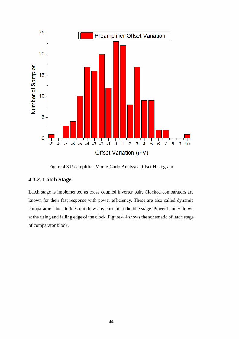
44
Figure 4.3 Preamplifier Monte-Carlo Analysis Offset Histogram
4.3.2. Latch Stage
Latch stage is implemented as cross coupled inverter pair. Clocked comparators are
known for their fast response with power efficiency. These are also called dynamic
comparators since it does not draw any current at the idle stage. Power is only drawn
at the rising and falling edge of the clock. Figure 4.4 shows the schematic of latch stage
of comparator block.

45
Figure 4.4 Comparator Latch Stage
Operation principle is based on hysteresis of the cross coupled inverters. When clock
is low, outputs of the both inverters are pulled up to VDD. At the rising edge of the
clock, reset PMOS transistors are turned off and NMOS transistor located in the middle
is turned on, letting current fall down through NMOS transistors of the inverters. At
that instant, NMOS input pair is in the linear mode such that its drain is grounded at
reset phase. According to the difference between input voltages, current flowing
through input pair differs, causing one side discharge faster than other. Therefore, an
imbalance occurs between cross coupled inverters and regenerative feedback forces to
toggle inverters to static position such that one of the inverters’ output become high
whereas other output becomes low. Therefore, decision is made according to the input
voltages. After that, at the falling edge of clock, both outputs are pulled to VDD again.
At each clock phase, this procedure repeats again and again. Output of the inverters
toggle with the every clock pulse, hence makes output data impractical to use. To deal
with this issue, SR latch is utilized. SR latch is useful that comparator output only
toggles once when ramp signal crosses input signal instead of every clock.
Figure 4.5 illustrates overall comparator output versus applied ramp signal and
sampled image signal. As ramp signal gradually crosses image signal, preamplifier
output is recovered from saturated mode. At the crossing instant, difference between
inputs is shown as amplified at the output of preamplifier. Then at the rising edge of
the clock, decision is made by dynamic comparator and output is toggled by SR latch.

46
Figure 4.5 Preamplifier and Latch stage output with respect to ramp signal and DC
image signal
4.5. Memory Circuit
Resolution of the ADC is 12 bit, hence 12 bit register with parallel load is required for
memory circuit implementation. When comparator triggers, counter’s output data is
parallel loaded into the memory circuit. To prevent any kind of unsettling issue, at the
rising edge of the master clock, counter is incremented and at the falling edge of the
master clock, comparator is toggled. Therefore, one can ensure that counter value is
settled when the comparator decision is made.
Memory circuit is realized as 12 bit parallel load register which is constituted of D Flip
Flops. At the rising edge of the comparator output, register parallel loads counter
output to save converted digital output. Figure 4.6 presents schematic of D Flip Flop
based register circuit.

47
Figure 4.6 3 bit Register Circuit consisted of D-Flip-Flops
At the end of the conversion, converted data is conveyed into another 12 bit register.
Pipelining is applied in order to allow one row time to the multiplexing. When column
ADC’s are converting a certain row, output registers are actually multiplexing previous
row’s data to the pads. Hence, first register can be realized as temporary register
whereas latter one is final storage.
4.6. Ramp Generator
Integrator based continuous ramp generator approach is applied for the ADC design.
DAC based approaches may cause non-linearity issues and requires buffer at the output
of the DAC due to the high load from shared column ADCs. In this integrator
approach, controlled current from high output impedance current source flows into the
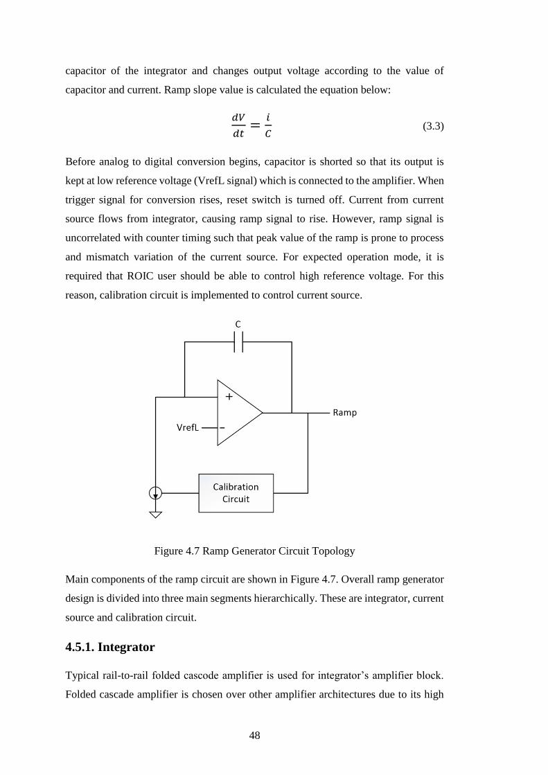
48
capacitor of the integrator and changes output voltage according to the value of
capacitor and current. Ramp slope value is calculated the equation below:
𝑑𝑉
𝑑𝑡=
𝑖
𝐶 (3.3)
Before analog to digital conversion begins, capacitor is shorted so that its output is
kept at low reference voltage (VrefL signal) which is connected to the amplifier. When
trigger signal for conversion rises, reset switch is turned off. Current from current
source flows from integrator, causing ramp signal to rise. However, ramp signal is
uncorrelated with counter timing such that peak value of the ramp is prone to process
and mismatch variation of the current source. For expected operation mode, it is
required that ROIC user should be able to control high reference voltage. For this
reason, calibration circuit is implemented to control current source.
Figure 4.7 Ramp Generator Circuit Topology
Main components of the ramp circuit are shown in Figure 4.7. Overall ramp generator
design is divided into three main segments hierarchically. These are integrator, current
source and calibration circuit.
4.5.1. Integrator
Typical rail-to-rail folded cascode amplifier is used for integrator’s amplifier block.
Folded cascade amplifier is chosen over other amplifier architectures due to its high

49
DC gain and rail-to-rail operation. Amplifier bandwidth requirement is high because
it should drive a significant amount of load consisting of column ADC comparators.
Also noise performance of the integrator is very important since ramp signal noise
directly contributes to ADC system noise. Figure 4.8 shows the folded cascade
amplifier schematic.
Figure 4.8 Rail-to-Rail Folded Cascode Amplifier
Amount of integration capacitor is important for ramp generator design. For fixed
ramp slope, larger capacitor requires more discharging current hence higher
transconductance value can be obtained. Therefore, noise level decreases.
Additionally, higher integration capacitance yields less kT/C noise.
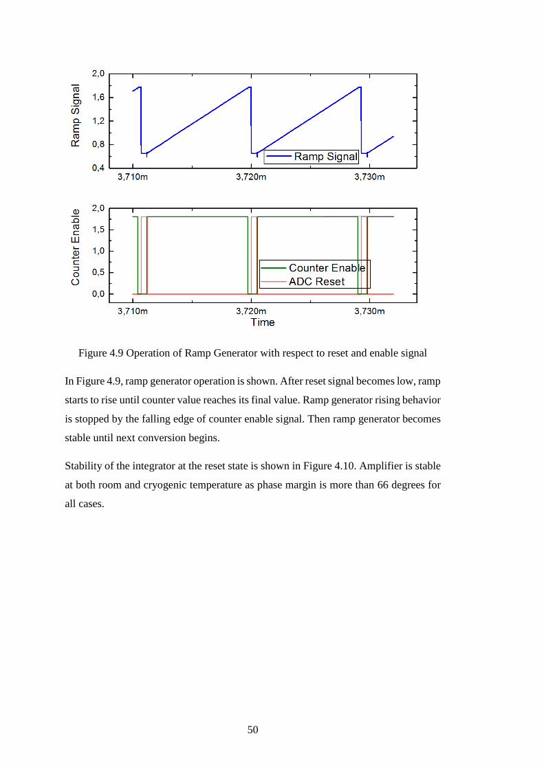
50
Figure 4.9 Operation of Ramp Generator with respect to reset and enable signal
In Figure 4.9, ramp generator operation is shown. After reset signal becomes low, ramp
starts to rise until counter value reaches its final value. Ramp generator rising behavior
is stopped by the falling edge of counter enable signal. Then ramp generator becomes
stable until next conversion begins.
Stability of the integrator at the reset state is shown in Figure 4.10. Amplifier is stable
at both room and cryogenic temperature as phase margin is more than 66 degrees for
all cases.
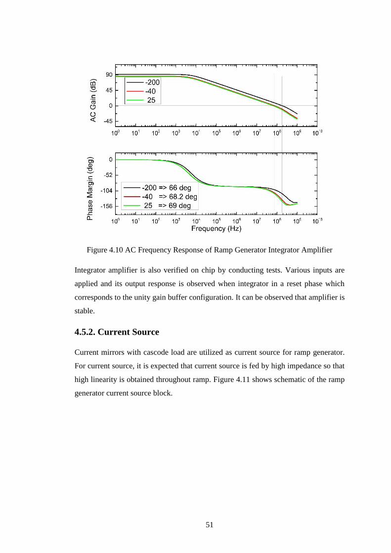
51
Figure 4.10 AC Frequency Response of Ramp Generator Integrator Amplifier
Integrator amplifier is also verified on chip by conducting tests. Various inputs are
applied and its output response is observed when integrator in a reset phase which
corresponds to the unity gain buffer configuration. It can be observed that amplifier is
stable.
4.5.2. Current Source
Current mirrors with cascode load are utilized as current source for ramp generator.
For current source, it is expected that current source is fed by high impedance so that
high linearity is obtained throughout ramp. Figure 4.11 shows schematic of the ramp
generator current source block.

52
Figure 4.11 Ramp Generator Current Source Circuit
Feedback from calibration circuit is applied as voltage signal. Hence, voltage to current
conversion should be done. For this reason, amplifier with feedback circuit is designed
[48]. With the help of the feedback and DC gain of the amplifier, provided input signal
is forced to the voltage above resistor. Hence voltage to current conversion is done
under Ohm’s Law such that current amount is controlled by resistor value. Generated
current is mirrored to four current sources in order to make current flow
programmable. Cascode transistors are added in order to increase impedance so that it
satisfies linearity. Linearity requirement for 12 bit operation can be denoted as [1]:
|k−k
k|
max= ε ≤
1
212 (3.4)
where k is slope. Ramp signal and its derivative which is slope are shown in Figure
4.12. According to the simulation result, max slope error is calculated by dividing max
error to the average slope. The calculation result below indicates that ramp generator
satisfies required linearity condition for 12 bit operation.
30
225k<
1
212 (3.5)
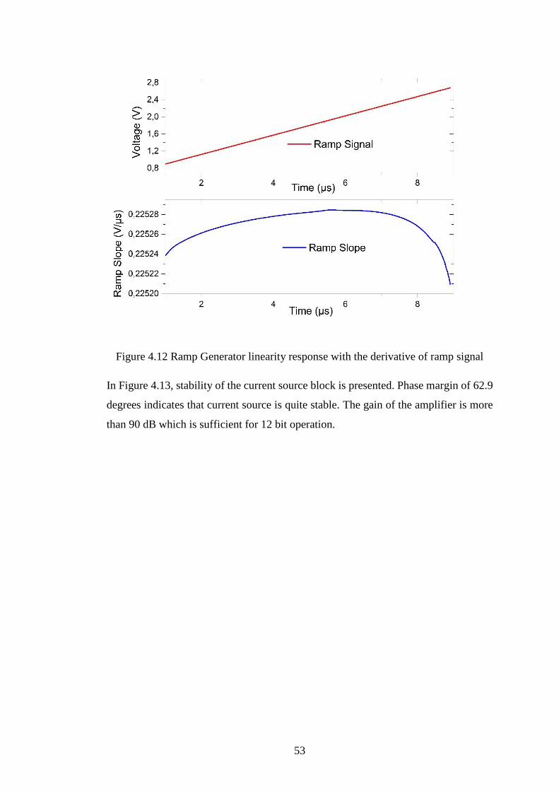
53
Figure 4.12 Ramp Generator linearity response with the derivative of ramp signal
In Figure 4.13, stability of the current source block is presented. Phase margin of 62.9
degrees indicates that current source is quite stable. The gain of the amplifier is more
than 90 dB which is sufficient for 12 bit operation.
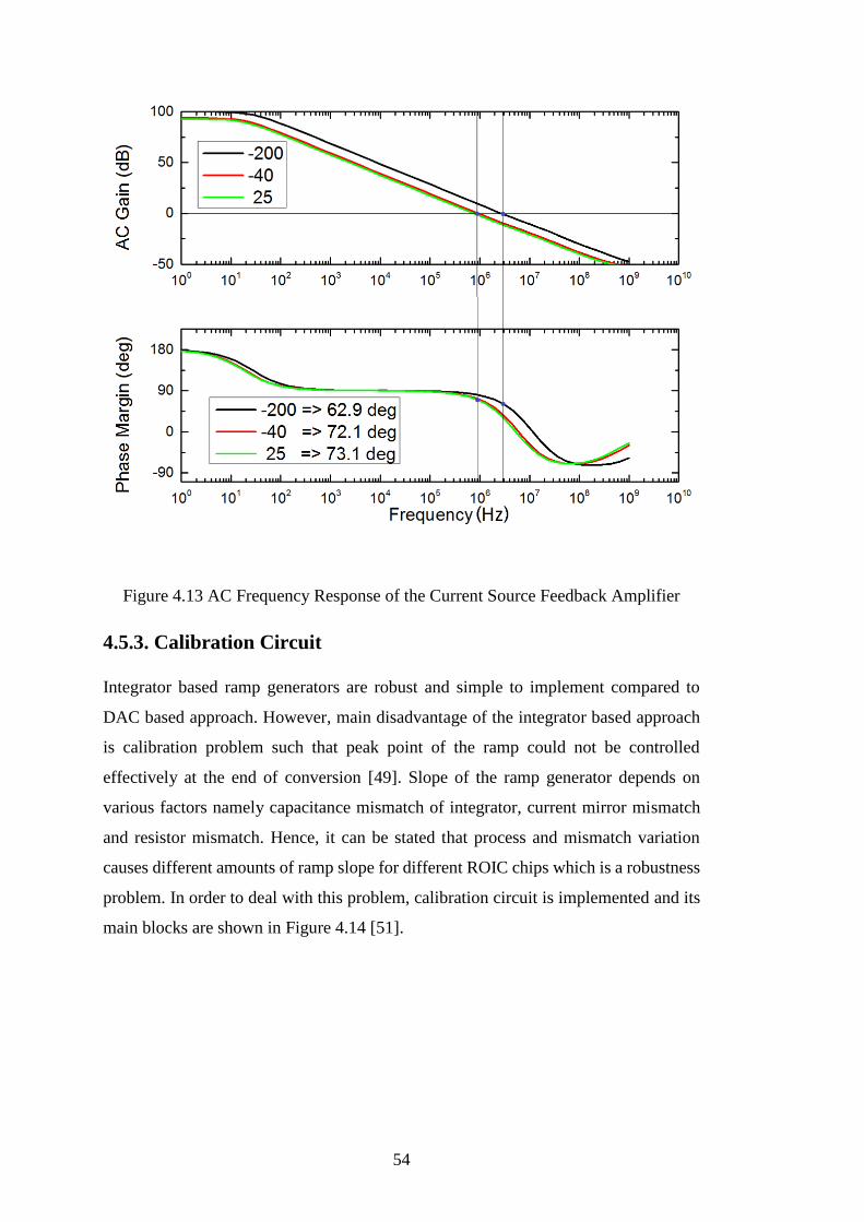
54
Figure 4.13 AC Frequency Response of the Current Source Feedback Amplifier
4.5.3. Calibration Circuit
Integrator based ramp generators are robust and simple to implement compared to
DAC based approach. However, main disadvantage of the integrator based approach
is calibration problem such that peak point of the ramp could not be controlled
effectively at the end of conversion [49]. Slope of the ramp generator depends on
various factors namely capacitance mismatch of integrator, current mirror mismatch
and resistor mismatch. Hence, it can be stated that process and mismatch variation
causes different amounts of ramp slope for different ROIC chips which is a robustness
problem. In order to deal with this problem, calibration circuit is implemented and its
main blocks are shown in Figure 4.14 [51].

55
Figure 4.14 Ramp Generator Calibration Feedback
At the end of analog to digital conversion, ramp signal’s peak voltage is compared
with VrefH signal which is expected high reference of the ramp signal. If peak value
of the ramp signal is lower than VrefH, then comparator output becomes high, causing
counter to be incremented. Digital count data is connected to a 12 bit DAC circuit,
which is responsible to drive analog feedback voltage to the current source according
to the counter data. As counter increments, output of DAC increases by approximately
0.7 mV, causing additional 7 nA current flow to the integrator for the next conversion.
Usage of 12 bit DAC makes this calibration very precise such that nominal current of
20 µA is achieved by 7 nA increments.
After numerous conversions, peak value of the ramp signal reaches beyond VrefH
signal. Then comparator output becomes low, hence counter is not incremented
anymore. With stable count data, DAC output stays fixed and ramp slope remains same
after all. In Table 4.3, effect of various DAC output voltages to the ramp swing is
given.
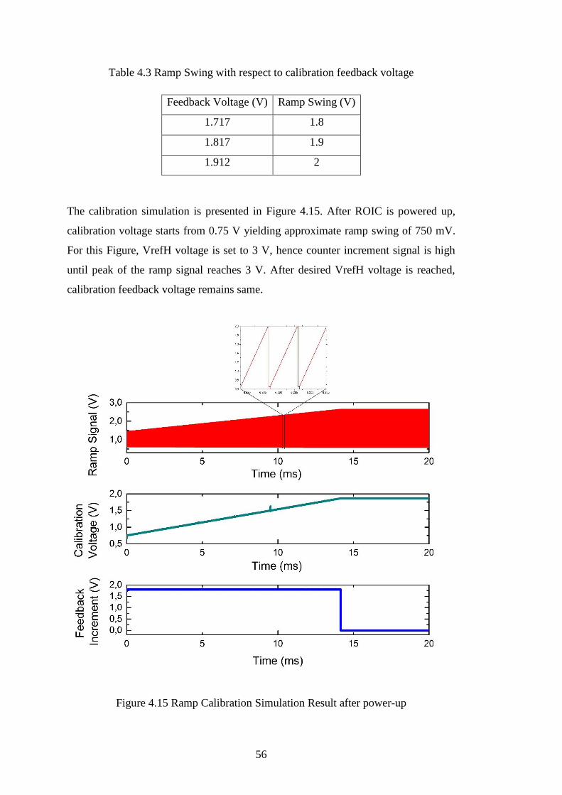
56
Table 4.3 Ramp Swing with respect to calibration feedback voltage
Feedback Voltage (V) Ramp Swing (V)
1.717 1.8
1.817 1.9
1.912 2
The calibration simulation is presented in Figure 4.15. After ROIC is powered up,
calibration voltage starts from 0.75 V yielding approximate ramp swing of 750 mV.
For this Figure, VrefH voltage is set to 3 V, hence counter increment signal is high
until peak of the ramp signal reaches 3 V. After desired VrefH voltage is reached,
calibration feedback voltage remains same.
Figure 4.15 Ramp Calibration Simulation Result after power-up
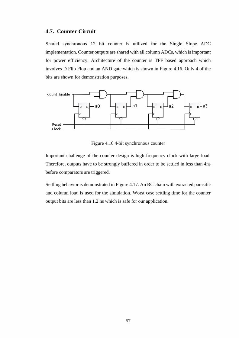
57
4.7. Counter Circuit
Shared synchronous 12 bit counter is utilized for the Single Slope ADC
implementation. Counter outputs are shared with all column ADCs, which is important
for power efficiency. Architecture of the counter is TFF based approach which
involves D Flip Flop and an AND gate which is shown in Figure 4.16. Only 4 of the
bits are shown for demonstration purposes.
Figure 4.16 4-bit synchronous counter
Important challenge of the counter design is high frequency clock with large load.
Therefore, outputs have to be strongly buffered in order to be settled in less than 4ns
before comparators are triggered.
Settling behavior is demonstrated in Figure 4.17. An RC chain with extracted parasitic
and column load is used for the simulation. Worst case settling time for the counter
output bits are less than 1.2 ns which is safe for our application.
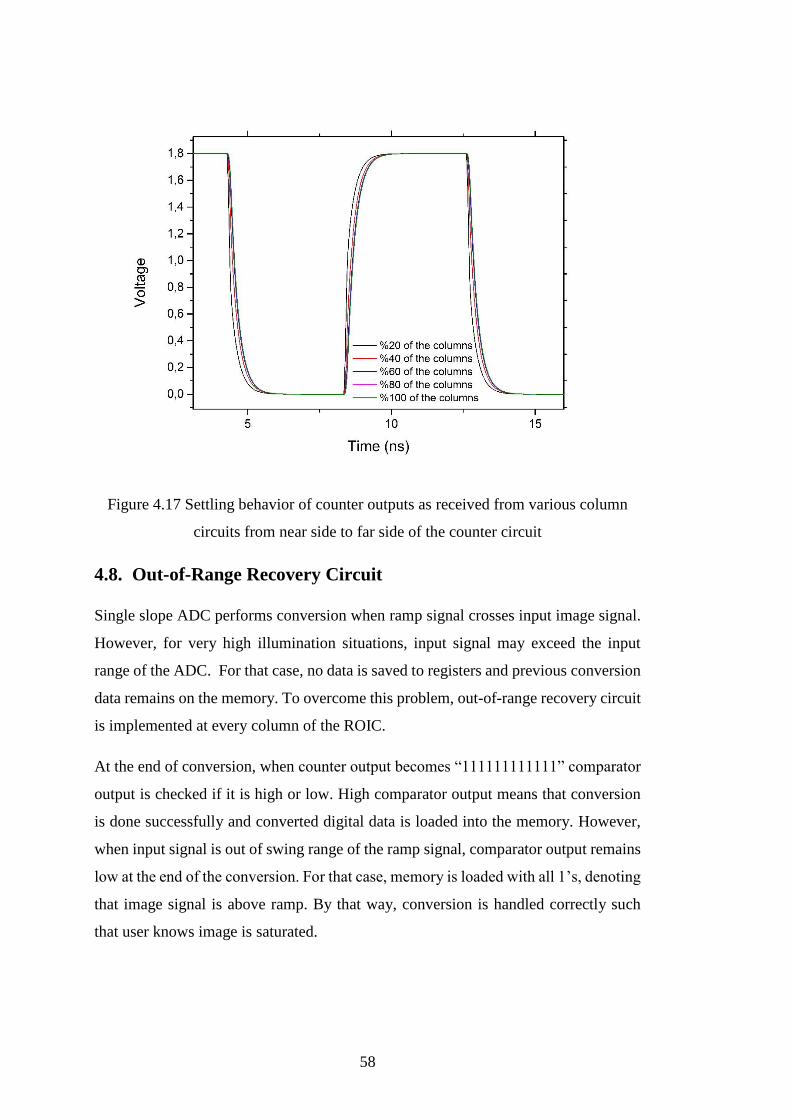
58
Figure 4.17 Settling behavior of counter outputs as received from various column
circuits from near side to far side of the counter circuit
4.8. Out-of-Range Recovery Circuit
Single slope ADC performs conversion when ramp signal crosses input image signal.
However, for very high illumination situations, input signal may exceed the input
range of the ADC. For that case, no data is saved to registers and previous conversion
data remains on the memory. To overcome this problem, out-of-range recovery circuit
is implemented at every column of the ROIC.
At the end of conversion, when counter output becomes “111111111111” comparator
output is checked if it is high or low. High comparator output means that conversion
is done successfully and converted digital data is loaded into the memory. However,
when input signal is out of swing range of the ramp signal, comparator output remains
low at the end of the conversion. For that case, memory is loaded with all 1’s, denoting
that image signal is above ramp. By that way, conversion is handled correctly such
that user knows image is saturated.

59
For the lower end case, ramp signal can be modified such that VrefL is lower from
variable gain amplifier reference voltage, so that input signal cannot be missed at the
lower end of the ramp. Therefore recovery circuit is only applied for lower end.
Figure 4.18 Out-of-range simulation and behavior of the memory output
In the Figure 4.18, out-of-range recovery circuit operation is presented. At the first
conversion, ramp signal crosses input signal as expected and counter data is loaded
into temporary register indicated by “reg” bus. At the end of conversion, temporary
data is transferred to the output memory denoted as “out” bus. For the second
conversion, input signal is out of ramp swing range hence comparator is not triggered.
However, out-of-range recovery circuit detects that comparator is not triggered and
loads “1111…” signal into the memory circuit.
4.9. Power Down Circuit
Single Slope ADC makes conversion when ramp signal crosses input signal. In order
to perform this, comparator makes decision at every clock pulse. After comparator is
triggered, the conversion is finalized and comparator is no longer needed until next
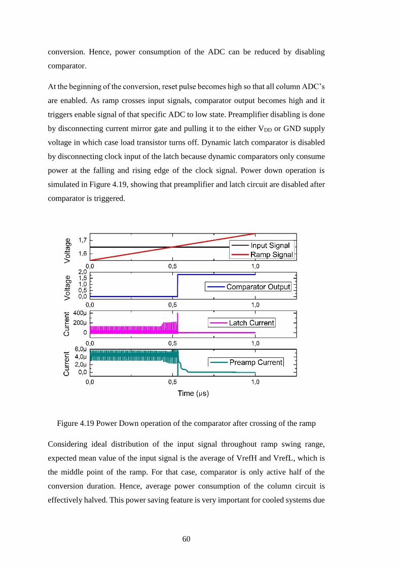
60
conversion. Hence, power consumption of the ADC can be reduced by disabling
comparator.
At the beginning of the conversion, reset pulse becomes high so that all column ADC’s
are enabled. As ramp crosses input signals, comparator output becomes high and it
triggers enable signal of that specific ADC to low state. Preamplifier disabling is done
by disconnecting current mirror gate and pulling it to the either VDD or GND supply
voltage in which case load transistor turns off. Dynamic latch comparator is disabled
by disconnecting clock input of the latch because dynamic comparators only consume
power at the falling and rising edge of the clock signal. Power down operation is
simulated in Figure 4.19, showing that preamplifier and latch circuit are disabled after
comparator is triggered.
Figure 4.19 Power Down operation of the comparator after crossing of the ramp
Considering ideal distribution of the input signal throughout ramp swing range,
expected mean value of the input signal is the average of VrefH and VrefL, which is
the middle point of the ramp. For that case, comparator is only active half of the
conversion duration. Hence, average power consumption of the column circuit is
effectively halved. This power saving feature is very important for cooled systems due

61
to limited cooling capacity of cryo-cooler. There is also a control bit to disable this
feature for testing purposes.


63
CHAPTER V
5. SIMULATION AND EXPERIMENTAL RESULTS
Single slope ADC is implemented as analyzed in the previous section and integrated
into digital ROIC. ROIC has been fabricated and tested hence ADC circuit is silicon
verified. In this section, simulated and experimental results are analyzed.
In Figure 5.1, photo of fabricated ROIC on a ceramic substrate is shown. ADC’s are
placed upper and lower side of the pixel array. Shared circuits are placed on the left
hand side.
Figure 5.1 Fabricated digital output ROIC

64
5.1. Top Level Simulation Results
Single Slope ADC is simulated extensively before tapeout in order to ensure its
operation. Figure 5.2 shows its main operation which indicates ramp crossing and
comparator triggering. Preamplifier amplifies the difference between ramp and input
signal, feeds it into latch stage for comparison. Output swing range of the preamplifier
is narrow; however, important thing is the amplified difference between signals which
latch stage is sufficient to resolve it.
Figure 5.2 Single Slope ADC operation
For noise simulations, FFT analysis is utilized with transient noise on. A sine wave is
applied at the input of the sample and hold stage and output data is analyzed. Digital
data is given to ideal DAC to reconstruct as analog signal. Digital data is processed by
MATLAB software to observe frequency response of the ADC.
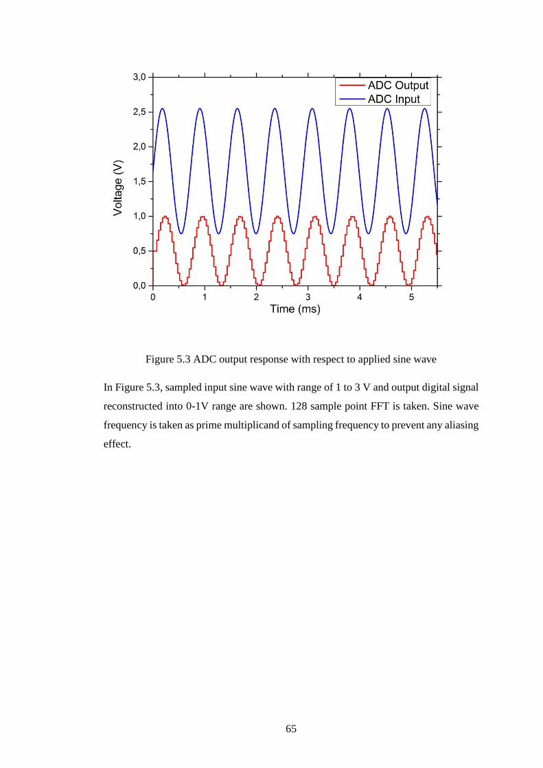
65
Figure 5.3 ADC output response with respect to applied sine wave
In Figure 5.3, sampled input sine wave with range of 1 to 3 V and output digital signal
reconstructed into 0-1V range are shown. 128 sample point FFT is taken. Sine wave
frequency is taken as prime multiplicand of sampling frequency to prevent any aliasing
effect.
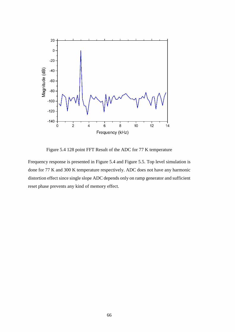
66
Figure 5.4 128 point FFT Result of the ADC for 77 K temperature
Frequency response is presented in Figure 5.4 and Figure 5.5. Top level simulation is
done for 77 K and 300 K temperature respectively. ADC does not have any harmonic
distortion effect since single slope ADC depends only on ramp generator and sufficient
reset phase prevents any kind of memory effect.
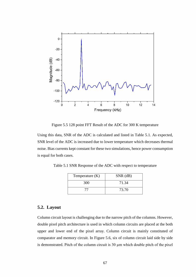
67
Figure 5.5 128 point FFT Result of the ADC for 300 K temperature
Using this data, SNR of the ADC is calculated and listed in Table 5.1. As expected,
SNR level of the ADC is increased due to lower temperature which decreases thermal
noise. Bias currents kept constant for these two simulations, hence power consumption
is equal for both cases.
Table 5.1 SNR Response of the ADC with respect to temperature
Temperature (K) SNR (dB)
300 71.34
77 73.70
5.2. Layout
Column circuit layout is challenging due to the narrow pitch of the columns. However,
double pixel pitch architecture is used in which column circuits are placed at the both
upper and lower end of the pixel array. Column circuit is mainly constituted of
comparator and memory circuit. In Figure 5.6, six of column circuit laid side by side
is demonstrated. Pitch of the column circuit is 30 µm which double pitch of the pixel
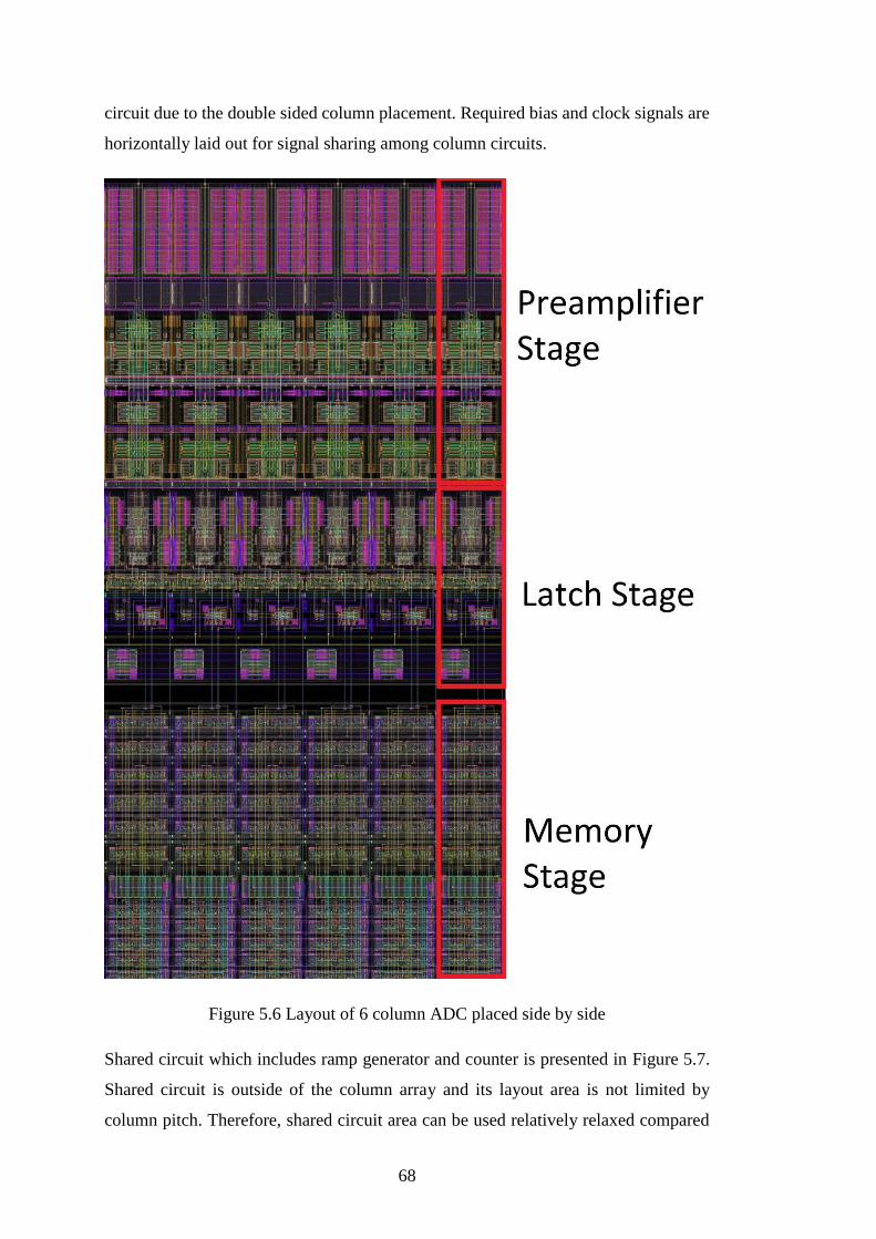
68
circuit due to the double sided column placement. Required bias and clock signals are
horizontally laid out for signal sharing among column circuits.
Figure 5.6 Layout of 6 column ADC placed side by side
Shared circuit which includes ramp generator and counter is presented in Figure 5.7.
Shared circuit is outside of the column array and its layout area is not limited by
column pitch. Therefore, shared circuit area can be used relatively relaxed compared

69
to the column circuit. Decoupling capacitors are added in order to reduce power supply
related noise.
Figure 5.7 Shared Circuit Layout
Sizes of column and shared blocks of ADC are given in Table 5.2. Column area has
pixel pitch limitation whereas shared blocks are not limited by area.
Table 5.2 Size of the Circuit Blocks
Circuit Block Size (µm × µm)
Column Circuit 370 x 30
Shared Circuit 660 x 540
5.3. Experimental Results
Silicon tests are performed under cryogenic temperature. For standalone ADC testing,
special test state is implemented as one test ADC converts injected input from external
PAD.
Test setup is shown in Figure 5.8 which is consisted of cryostat, analog PCB board
and digital PCB interface board. Programming is done through computer and
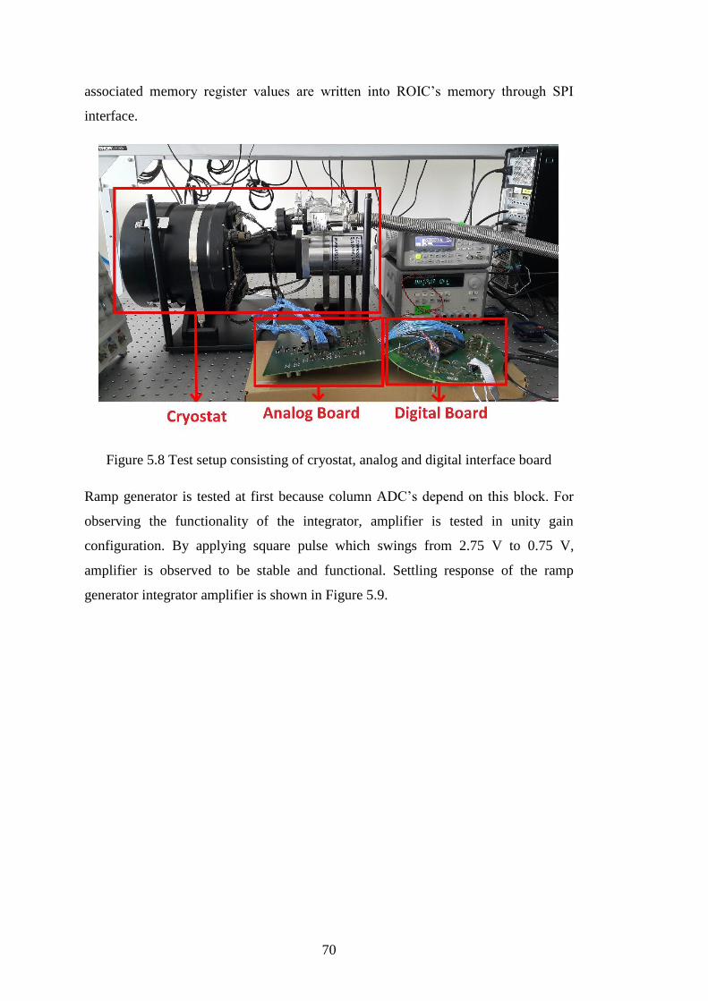
70
associated memory register values are written into ROIC’s memory through SPI
interface.
Figure 5.8 Test setup consisting of cryostat, analog and digital interface board
Ramp generator is tested at first because column ADC’s depend on this block. For
observing the functionality of the integrator, amplifier is tested in unity gain
configuration. By applying square pulse which swings from 2.75 V to 0.75 V,
amplifier is observed to be stable and functional. Settling response of the ramp
generator integrator amplifier is shown in Figure 5.9.
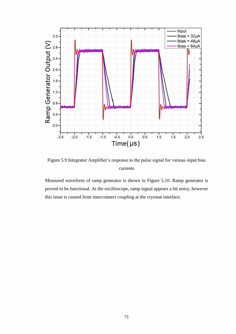
71
Figure 5.9 Integrator Amplifier’s response to the pulse signal for various input bias
currents
Measured waveform of ramp generator is shown in Figure 5.10. Ramp generator is
proved to be functional. At the oscilloscope, ramp signal appears a bit noisy, however
this issue is caused from interconnect coupling at the cryostat interface.

72
Figure 5.10 Ramp Generator Measured Waveform
Ramp generator is tested by two different methods. It is first driven by externally
generated reference voltages, afterwards internally generated voltages are used. Result
is observed to be same. This means that internal reference generator is operational.
After power up sequence, auto calibration circuit calibrates ramp waveform such that
it will reach high reference voltage at the final instant of the conversion.
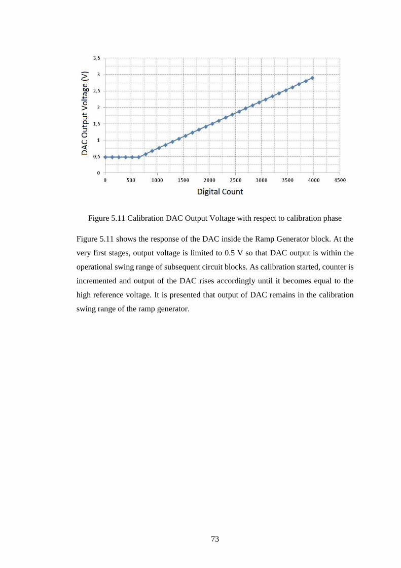
73
Figure 5.11 Calibration DAC Output Voltage with respect to calibration phase
Figure 5.11 shows the response of the DAC inside the Ramp Generator block. At the
very first stages, output voltage is limited to 0.5 V so that DAC output is within the
operational swing range of subsequent circuit blocks. As calibration started, counter is
incremented and output of the DAC rises accordingly until it becomes equal to the
high reference voltage. It is presented that output of DAC remains in the calibration
swing range of the ramp generator.

74
Figure 5.12 Ramp Slope change for various calibration voltages
Another test is conducted in order to observe effect of ramp calibration feedback
voltage shown in Figure 5.12. Ramp Calibration feedback is disabled and externally
applied voltage signal is injected to the input of current source block of the ramp
generator. According to the value of calibration voltage, the slope of the ramp changes
accordingly and ramp starts at the same low reference voltage as expected.

75
Figure 5.13 ADC Digital Response with respect to integration time for various
injected detector currents
In Figure 5.13, ADC’s output response is projected with respect to integration time.
Longer integration yields higher pixel swing, hence ADC output response will increase
linearly. However, pixel is saturated after some time reaching its full well capacity
meaning that pixel is saturated. After saturation, ROIC response is not linear anymore.
In the figure 5.13, it is also shown that higher detector currents saturate pixel faster.
ADC Output response with respect to injected input voltage is presented in Figure
5.14. Various resolution operations are shown for 12 bit, 11 bit and 10 bit. As expected
digital output slope changes as resolution of the ADC increases.

76
Figure 5.14 ADC Output Response with respect to injected input voltage for various
ADC resolution
For noise calculation, histogram method is used as well as FFT method. Histogram
method requires that DC input is applied to the input of the ADC and its output is
observed. Digital data is acquired by FPGA card and conveyed to the ROIC test
software. Precision DC analog signal is applied to the input of ADC and calibrated to
the middle of the LSB bit range in order to condense output probability on that specific
bit. Then code errors are observed at previous and subsequent code. This indicates
noise performance of the ADC. According to the two histogram results, which have
code errors on both sides, standard deviation is calculated as 0.1796 and 0.1339 bits
which corresponds to ENOB of 11.6552 and 11.5963 bits.
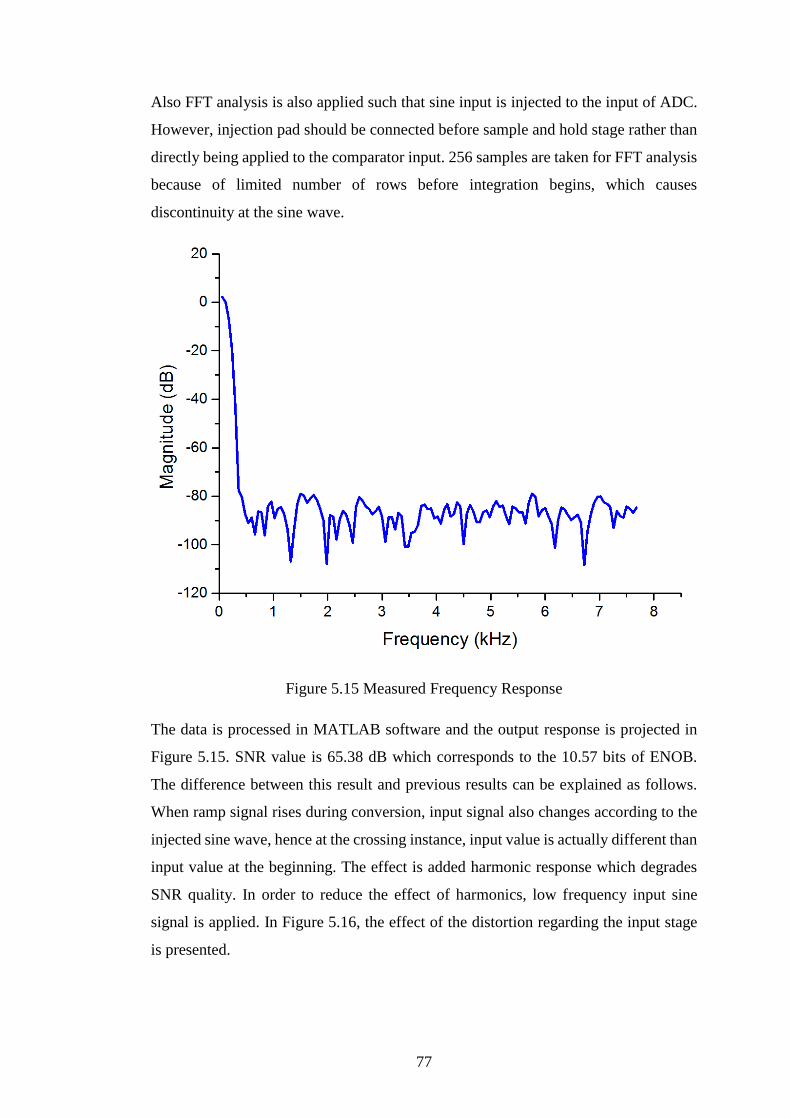
77
Also FFT analysis is also applied such that sine input is injected to the input of ADC.
However, injection pad should be connected before sample and hold stage rather than
directly being applied to the comparator input. 256 samples are taken for FFT analysis
because of limited number of rows before integration begins, which causes
discontinuity at the sine wave.
Figure 5.15 Measured Frequency Response
The data is processed in MATLAB software and the output response is projected in
Figure 5.15. SNR value is 65.38 dB which corresponds to the 10.57 bits of ENOB.
The difference between this result and previous results can be explained as follows.
When ramp signal rises during conversion, input signal also changes according to the
injected sine wave, hence at the crossing instance, input value is actually different than
input value at the beginning. The effect is added harmonic response which degrades
SNR quality. In order to reduce the effect of harmonics, low frequency input sine
signal is applied. In Figure 5.16, the effect of the distortion regarding the input stage
is presented.
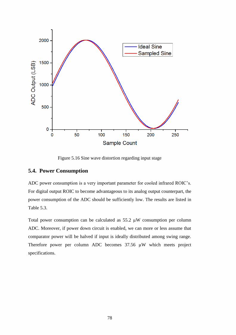
78
Figure 5.16 Sine wave distortion regarding input stage
5.4. Power Consumption
ADC power consumption is a very important parameter for cooled infrared ROIC’s.
For digital output ROIC to become advantageous to its analog output counterpart, the
power consumption of the ADC should be sufficiently low. The results are listed in
Table 5.3.
Total power consumption can be calculated as 55.2 µW consumption per column
ADC. Moreover, if power down circuit is enabled, we can more or less assume that
comparator power will be halved if input is ideally distributed among swing range.
Therefore power per column ADC becomes 37.56 µW which meets project
specifications.
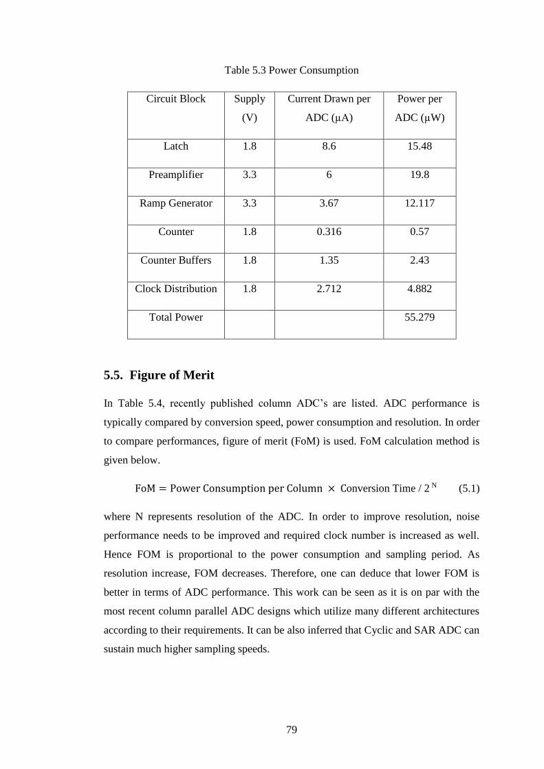
79
Table 5.3 Power Consumption
Circuit Block Supply
(V)
Current Drawn per
ADC (µA)
Power per
ADC (µW)
Latch 1.8 8.6 15.48
Preamplifier 3.3 6 19.8
Ramp Generator 3.3 3.67 12.117
Counter 1.8 0.316 0.57
Counter Buffers 1.8 1.35 2.43
Clock Distribution 1.8 2.712 4.882
Total Power 55.279
5.5. Figure of Merit
In Table 5.4, recently published column ADC’s are listed. ADC performance is
typically compared by conversion speed, power consumption and resolution. In order
to compare performances, figure of merit (FoM) is used. FoM calculation method is
given below.
FoM = Power Consumption per Column × Conversion Time / 2 N (5.1)
where N represents resolution of the ADC. In order to improve resolution, noise
performance needs to be improved and required clock number is increased as well.
Hence FOM is proportional to the power consumption and sampling period. As
resolution increase, FOM decreases. Therefore, one can deduce that lower FOM is
better in terms of ADC performance. This work can be seen as it is on par with the
most recent column parallel ADC designs which utilize many different architectures
according to their requirements. It can be also inferred that Cyclic and SAR ADC can
sustain much higher sampling speeds.

80
Table 5.4 Figure of Merit of the column ADC’s
ADC Bit
ADC Sample
Freqency
(KS/s)
Total
Power (mW)
FoM
(pJ/conv)
SS [12] 10 138.8 360 1.158
MRSS [20] 10 62.5 52 2.46
SAR [24] 12 250 1085 0.488
SAR [52] 10 565 700 0.7
Cyclic [33] 13 217 297 0.37
Cyclic [53] 12 2000 1000 0.23
Sigma Delta [27] 12 145.9 180 0.178
2 step SS [21] 12 250 36 0.584
DLL based SS [10] 12 330 82 0.182
This Work 12 27 14.45 0.341
This Work 10 107.5 14.45 0.341
All of the above listed work is implemented for visible image sensors where market
demand is relatively strong and competition is fierce. Therefore, many academic
researches are being funded and many publications are present in the literature. On the
other hand, infrared imaging market is limited to the military applications where
knowledge sharing is limited. There are few publications regarding infrared ROIC’s
and the available ones are absent from detail. Due to this reason, figure of merit data
consists of visible image sensors instead of infrared ROIC’s.
From the given FoM values, the work presented in this thesis can be considered
competitive compared to the other work. Some of the presented work is better in terms
81
of power consumption. This phenomenon can be explained by advanced CMOS
technology and efficient ADC architectures. However, FoM of the implemented
single slope ADC found to be more efficient than many of the presented research
papers.

83
CHAPTER VI
6. CONCLUSION AND FUTURE WORK
6.1. Conclusion
The research presented in this dissertation involves design of a Column Parallel Single
Slope ADC implemented within digital output ROIC. Digital output ROIC can be
hybridized with various types of detector materials to serve different bands of the
spectrum ranging from UV to LWIR with proper pixel circuit. Within the framework
of this thesis, Digital Output ROIC has been fabricated with 0.18 µm commercial
CMOS process with direct injection type pixel circuit to serve LWIR and MWIR bands
of the spectrum.
Digital output ROIC’s have several advantages with respect to analog output ROIC’s
such as higher system compactness, removal of ADC proxy card, invulnerability to
environment noise with equivalent power consumption. For that respect, column
parallel approach is evaluated to be an efficient method to implement digital ROIC in
terms of area and speed optimization.
Based on the achievements and the results of this work, following conclusions can be
drawn:
1. As there are several approaches to implement column parallel ADC, Single
Slope ADC is chosen over other architectures for its efficient layout area
footprint in columns, low power consumption as most of the circuits are shared
and design simplicity. To serve different applications, ADC is implemented as
10 to 12 bit programmable with 107.5 kHz and 27 kHz conversion rate
respectively.

84
2. Cryogenic temperatures cause significant parameter shifts on transistors and
foundry provided transistor models are not valid at those temperatures.
Implementation has been done carefully considering unfavorable effects by
providing sufficient redundancy for all blocks. In this work, ADC
implementation is done by ensuring that every voltage and current bias made
programmable in order to sustain operability of the ADC at the optimum
conditions.
3. Analog ramp generator is introduced instead of DAC based approach in order
to reduce power consumption of the system. Analog ramp generators are prone
to process and mismatch variations and cryogenic parameter shifts which cause
significant input voltage swing variations among chips. Feedback based ramp
calibration is introduced to overcome this phenomenon. After power-up
sequence of the ROIC, implemented calibration circuit automatically adjusts
ADC swing range to the reference voltages. Those reference voltages are either
on-chip bandgap generated or externally applied in order to provide
redundancy.
4. To reduce power consumption, a special power-down circuit is implemented
so that it benefits from operation principles of Single Slope ADC. Comparator
circuit is powered down when ramp signal crosses input signal. Moreover, out-
of-range recovery circuit is introduced in order to be able to handle conversion
for very bright conditions in which pixels saturate.
5. ADC circuit layout is carried out carefully such that ADC fits into narrow
column pitch. Also, each column ADC shares common bias, clock and ramp
signal which are conveyed side by side. Clock distributions are done by clock-
tree approach to ensure that each ADC receives clock synchronously.
Distribution of all these signals throughout large ROIC with proper delay and
ohmic drop is carried out successfully.
6. ADC integration into ROIC is done within overall timing constraints. In order
to handle digitization operation concurrent with readout operation, pipeline
readout method is introduced to increase overall image sensor speed. In this
method, while gain stage is reading out a specific row, ADC is converting
previously sampled row. Additional pipeline stage is also introduced at the
output stage. Converted digital data is written into memory circuits after
85
conversion, allowing data of the previous row to be transferred in next row. By
these two pipeline stages, conversion can be completed in a full row duration.
7. Functionality of the ADC is verified with detailed electrical tests. Block by
block verification is done to ensure each sub-blocks operability. Also,
standalone ADC tests are conducted, excluding all other circuit elements to
assess true performance of the ADC. In standalone mode, ADC can fulfill more
than 70 dB performance which is compatible with our system specifications.
8. Column ADC power consumption is less than 40 µW which is less than
average power consumed by line amplifiers used in analog output ROICs.
Therefore, digital output ROIC is proven to be more power efficient than its
analog output counterparts.
It can be concluded that major achievement of this work is the development of an ADC
circuit for a ROIC. With this implementation, ROIC has a digital output and overall
power can be kept the same. Additionally, system volume is reduced by elimination of
proxy card. Also digital output is resistant to the environmental noise which is caused
by Dewar interface and outside medium.
6.2. Future Work
12 bit ADC implementation is done successfully within the scope of this thesis.
However, for the future infrared systems, high FPS operation is required. Moreover,
for more sensitive systems, higher NETD values are necessary. Therefore, ROIC SNR
performance should be improved by increasing resolution to 14 bits within same power
consumption. As future work, ADC resolution and sampling speed will be increased.
Additionally, this work will be tested with qualified high performance detector to
observe system performance.


87
REFERENCES
[1] Y. Liu, "The Design of a High Dynamic Range CMOS Image Sensor in 110nm
Technology," Dissertation for the Degree of Master of Science, Delft University of
Technology, 2012
[2] I. Takayanagi, J. Nakamura, “High Resolution CMOS video sensors”, Proceedings
of the IEEE, 2012
[3] B. Pain, E.R. Fossum, "Approaches and analysis for on-focal-plane analog-to-
digital conversion," in Infrared Readout Electronics II, Proc. SPIE, vol. 2226, pp. 208-
218, 1994
[4] M. Zécri, P. Maillart, E. Sanson, G. Decaens, X. Lefoul, L. Baud, "Advanced
ROICs design for cooled IR detectors," Proc. of SPIE Vol. 6940 69402X-1, 2008
[5] O. Nesher, P.C. Klipstein, "High-performance IR detectors at SCD present and
future", Opto-Electronics Review 14(1), 61–70, 2006
[6] S. Eminoglu, "Uncooled Infrared Focal Plane Arrays With Integrated Readout
Circuitry Using Mems And Standard Cmos Technologies," Dissertation for the Degree
of Doctor of Philosophy, METU, 2003
[7] METU EE 419 Solid State Devices Lecture Notes, Cengiz Besikci, 2012
[8] S. Elkind, A. Adin, I. Nevo and A. B. Marhasev, "Focal plane processor with a
digital video output for InSb detectors," Proc. SPIE, vol. 4820, 2003
[9] G. DECAENS, et al. "Ultra low power ADC on chip for high performance IR
detector", Proc. of SPIE Vol. 7298, 2009
[10] Jia Guo, "DLL Based Single Slope ADC for CMOS Image Sensor Column
Readout," Dissertation for the Degree of Master of Science, Delft University of
Technology, 2011
[11] I. Takayanagi, M. Shirakawa, K. Mitani, M. Sugawara, S. Iversen, J. Moholt, J.
Nakamura, and E. R. Fossum, “A 1.25-inch 60-frames/s 8.3-M-pixel digital-output

88
CMOS image sensor,” IEEE J. Solid-State Circuits, vol. 40, no. 11, pp. 2305–2314,
Nov. 2005
[12] S. Yoshihara, M. Kikuchi, Y. Ito, Y. Inada, S. Kuramochi, H. Wakabayashi, M.
Okano, K. Koseki, H. Kuriyama, J. Inutsuka, A. Tajima, T. Nakajima, Y. Kudoh, F.
Koga, Y. Kasagi, S. Watanabe, and T. Nomoto, “A 1/1.8-inch 6.4 Mpixel 60 frames/s
CMOS image sensor with seamless mode change” in Int. Solid-State Circuits Conf.
Dig. Tech. Papers, 2006, pp. 492–493.
[13] Arnaud Peizerat, Jean-Pierre Rostaing, Noureddine Zitouni, Nicolas Baier,
Fabrice Guellec, Rémi Jalby, Michael Tchagaspanian, "An 88dB SNR, 30μm pixel
pitch Infra-Red image sensor with a 2-step 16 bit A/D conversion," Symposium on
VLSI Circuits Digest of Technical Papers, 2012
[14] Cheng Ma, "Pixel ADC Design For Hybrid CMOS Image Sensors," Dissertation
for the Degree of Master of Science, Delft University of Technology, 2010
[15] Zeljko Ignjatovic, Mark F. Bocko "A 0.88nW/pixel, 99.6 dB Linear-Dynamic-
Range Fully-Digital Image Sensor Employing a Pixel-Level Sigma-Delta ADC,"
Symposium on VLSI Circuits Digest of Technical Papers, 2006
[16] M. Snoeij, A. Theuwissen, K. Makinwa, and J. Huijsing, “A CMOS imager with
column-level adc using dynamic column fixed-pattern noise reduction,” IEEE J. Solid-
State Circuits, vol. 41, no. 12, pp. 3007–3015, Dec. 2006
[17] Manuel Innocent, "General introduction to CMOS image sensors," CNES
[18] Juan A. Lenero-Bardallo, Jorge Fernandez-Bernia and Angel Rodriguez-
Vazquez, "Review of ADCs for imaging," Proc. of SPIE-IS&T Vol. 9022, 2014
[19] Albert Theuwissen, "CMOS Image Sensors State-Of-The-Art and Future
Perspectives," Solid State Electronics 52.9, 2008
[20] M. F. Snoeij, A. J. P. Theuwissen, K. A. A. Makinwa, and J. H. Huijsing,
“Multiple-ramp column-parallel ADC architectures for CMOS image sensors”, IEEE
J. Solid-State Circuits, vol. 42, no. 12, pp. 2968–2977, Dec. 2007

89
[21] Jeonghwan Lee, Seunghyun Lim, and Gunhee Han, “A 10b Column-wise Two-
step Single-slope ADC for High-speed CMOS Image Sensor”, Proc. IEEE Int. Image
Sensor Workshop, 2007
[22] Woongtaek Lim, Jongyoon Hwang, Dongjoo Kim, Shiwon Jeon, Suho Son, and
Minkyu Song, "A Low Noise CMOS Image Sensor with a 14-bit Two-Step Single-
Slope ADC and a Column Self-Calibration Technique," Sensors 14.7, 2014
[23] Marcel Pelgrom, "Analog-to-Digital Conversion", Springer 2010
[24] Shinichiro Matsuo, Timothy J. Bales, Masahiro Shoda, Shinji Osawa, Katsuyuki
Kawamura, Anders Andersson, Munirul Haque, Hidenari Honda, Bryan Almond,
Yaowu Mo, Jeffrey Gleason, Tony Chow, and Isao Takayanagi, "8.9-Megapixel Video
Image Sensor With 14-b Column-Parallel SA-ADC", Ieee Transactions On Electron
Devices, VOL. 56, NO. 11, 2009
[25] Min-Seok Shin, Jong-Boo Kim, Min-Kyu Kim,Yun-Rae Jo, and Oh-Kyong
Kwon, "A 1.92-Megapixel CMOS Image Sensor With Column-Parallel Low-Power
and Area-Efficient SA-ADCs," Ieee Transactions On Electron Devices, VOL. 59, NO.
6, JUNE 2012
[26] F. Guellec, et al. "Sigma-delta column-wise A/D conversion for cooled ROIC",
Proc. of SPIE Vol. 6542, 2007
[27] Y. Chae and G. Han, “Low voltage, low power, inverter-based switched-capacitor
delta-sigma modulator,” IEEE J. Solid-State Circuits, vol. 44, no. 2, pp. 458–472, Feb.
2009.
[28] A. Mahmoodi and D. Joseph, "Optimization of delta-sigma ADC for column-
level data conversion in CMOS image sensors," IEEE Proc. Instrumentation and
Measurement Technology, pp. 1-6, May 2007
[29] Gun-Hee Yun, Min-Kyu Kim, Jong-Boo Kim, Min-Seok Shin, Oh-Kyong Kwon,
“A Low-Power 12-bit 2nd-Order ƩΔ Analog-toDigital Converter for CMOS Image
Sensors”, IEEE ICECS 2010
[30] Y. Chae, J. Cheon, S. Lim, M. Kwon, K. Yoo, W. Jung, D.-H. Lee, S. Ham, and
G. Han, “A 2.1 M pixels, 120 frame/s CMOS image sensor with column-parallel
90
Sigma Delta ADC architecture”, IEEE J. Solid-State Circuits,vol. 46, no. 1, pp. 236–
247, Jan. 2011
[31] Min-Woong Seo, "A Study on Low-Noise High Dynamic Range High Resolution
CMOS lmage Sensors with Folding-!nteg ration/Cyclic ADCs," Dissertation for the
Degree of Doctor of Philosophy, Shizuoka University, 2012
[32] Deyan Levski Dimitrov, "A Cyclic Analog to Digital Converter for CMOS image
sensors," Dissertation for the Degree of Master of Science, 2013
[33] J.-H. Park, S. Aoyama, T. Watanabe, K. Isobe, and S. Kawahito, “A high-speed
low-noise CMOS image sensor with 13-b column-parallel single-ended cyclic ADCs”,
IEEE Trans. Electron Devices, vol. 56, no. 11,pp. 2414–2422, Nov. 2009
[34] Franco Maloberti, "Data Converters," Springer, 2007
[35] Nayeon Cho, Bongsub Song, Kwangsoo Kim, Jinwook Burm, Sang-Wook Han,
“A VGA CMOS Image Sensor with 11-bit column parallel single-slope ADCs”,
ISOCC 2010
[36] Wu Gao, et al. "A 12-bit Low-Power Multi-Channel Ramp ADC Using Digital
DLL Techniques for High-Energy Physics and Biomedical Imaging" IEEE
Transactions on Instrumentation and Measurement, 2010
[37] HeungJun Jeon, "Low-Power High-Speed Low-Offset Fully Dynamic Cmos
Latched Comparator" Dissertation for the Degree of Master of Science Northeastern
University, 2010
[38] Nikoozadeh and B. Murmann, “An Analysis of Latch Comparator Offset Due to
Load Capacitor Mismatch,” IEEE Trans. Circuits Syst. II: Exp. Briefs, vol. 53, no. 12,
pp. 1398-1402, Dec. 2006
[39] He, Jun, et al. "Analyses of static and dynamic random offset voltages in dynamic
comparators." Circuits and Systems I: Regular Papers, IEEE Transactions on 56.5,
2009
[40] M.F. Snoeij, A.J.P. Theuwissen and J.H. Huijsing, "A 1.8V 3.2μW Comparator
for Use in a CMOS Imager Column-Level Single-Slope ADC," IEEE ISCAS, 2005
91
[41] Yibing(Michelle) Wang, Sang-Soo Lee, Kwang Oh Kim, “Comparison of Several
Ramp Generator Designs for Column-Parallel Single Slope ADCs” Proc. Int. Image
Sensor Conf., 2009
[42] Tetsuya Iizuka, Kunihiro Asada, "All-Digital ramp waveform generator for tow-
step single-slope ADC", IEICE 2011
[43] Sakkarapani Balagopal, Suat Ay, "An On-chip Ramp Generator for Single Slope
Look Ahead Ramp (SSLAR) ADC" IEEE MWSCAS, 2009
[44] Benoit Provost, Edgar Sánchez-Sinencio, "On-Chip Ramp Generators for Mixed-
Signal BIST and ADC Self-Test", IEEE JSSC, VOL. 38, NO. 2, FEBRUARY 2003
[45] Ziqi Song, Dong Wu, Yanzhao Shen, Jun Xu, "Column-Parallel Integrating ADCs
for Infrared Image Sensor" IEEE ICSICT, 2010
[46] Yue Chen, Yang Xu, Adri J. Mierop, Albert J. P. Theuwissen, “Column-Parallel
Digital Correlated Multiple Sampling for Low-Noise CMOS Image Sensors”, IEEE
Sensors Journal, Vol. 12, No. 4, April 2012
[47] Y. Nitta, Y. Muramatsu, K. Amano, T. Toyama, J. Yamamoto, K. Mishina, A.
Suzuki, T. Taura, A. Kato, M. Kikuchi, Y. Yasui, H. Nomura, and N. Fukushima,
“High-speed digital double sampling with analog CDS on column paralel ADC
architecture for low-noise active pixel sensor” in Int. Solid-State Circuits Conf. Dig.
Tech. Papers, Feb. 2006, pp. 500–501
[48] Wen-Ta Lee, et al. "High Precision Ramp Generator for Low Cost ADC Test,"
IEEE ICSICT, 2008
[49] Seog-Heon Ham, et al. "Image Sensor Using Auto-Calibrated Ramp Signal For
Improved Image Quality and Driving Method Thereof", US Patent 7,679,542, 2010
[50] Christer Jansson, et al. "Linear, Polynomial and Exponential Ramp Generators
with Automatic Slope Adjustment" Ieee Transactions On Circuits And Systems-I
VOL. 41, NO. 2, 1994
[51] F. Azaïs, S. Bernard, Y. Bertrand, X. Michel, M. Renovell, "A low-cost adaptive
ramp generator for analog BIST applications," IEEE VTS, 2001

92
[52] Alexander I., A High-Speed, 240-Frames/s, 4.1-Mpixel CMOS Sensor. IEEE
Transactions on Electron Devices, 2003. Volume: 50, Issue: 1. Page: 130 – 135
[53] Furuta, M., A High-Speed, High-Sensitivity Digital CMOS Image Sensor With a
Global Shutter and 12-bit Column-Parallel Cyclic A/D Converters, IEEE Journal of
Solid-State Circuits, 2007. Volume: 42, Issue: 4. Page: 766 – 774