Embed Size (px)
Citation preview

Design and Implementation of Digital Current Mode Control
by
Siyu He
A dissertation submitted to the Graduate Faculty of
Auburn University
in partial fulfillment of the
requirements for the Degree of
Doctor of Philosophy
Auburn, Alabama
May 10, 2015
Key words: Current mode control, Digital implementation, Switch-mode power supplies
Analog Control, Small-signal modeling
Copyright 2015 by Siyu He
Approved by
Robert Mark Nelms, Chair, Professor of Electrical Engineering
John York Hung, Professor of Electrical Engineering
Steve Mark Halpin, Alabama Power Company Distinguished Professor Electrical Engineering
Victor Peter Nelson, Professor of Electrical Engineering

ii
Abstract
Presented in this dissertation are three digital control methods of current mode
control for switch-mode power supplies. Both the current and voltage loop are implemented on
the digital processor. Digital versions of peak current mode control (predictive current mode
control), average current mode control and I2 average current mode control are proposed and
investigated in sequence. Issues of noise filtering, high frequency analog-to-digital (ADC)
sampling and digital PWM modulations are discussed.
Since the peak current mode control (PCM) finds wide application in low-to-medium
power DC-DC converters, the digital predictive current mode control is first presented in this
dissertation which is the equivalent digital version of PCM. The control law is derived based on
the steady state operation of analog PCM control, which only needs one sample per cycle to
estimate the current peak signal. The small-signal model is developed and verified by
measurements from an AP300 network analyzer. Because of the common configuration for the
digital current mode control methods, the small-signal model developed for predictive current
mode control can be used as a basis for other digital current mode control.
Then, three digital implementations of average current mode control are discussed which
are the basis for the digital I2 average current mode control in the later chapter. The advantages
and disadvantages of each implementation are compared. The modification of the small-signal
model for predictive current mode control is developed to predict the frequency response of digital
average current mode control.

iii
I2 average current mode control was proposed in 2013, a small-signal modeling for an
analog implemented I2 average current mode is presented. This small-signal model successfully
predicts the “sub-harmonic” oscillation when the duty cycle is close, or greater than 0.5. By
paralleling the current loops of peak current mode and average current mode, the digital I2 average
current mode control is designed using predictive current mode control and digital average current
mode control.
A TMS320F2812 DSP controlled boost converter is built to serve as a prototype to
experimentally demonstrate the feasibility of these digital current mode control technique.

iv
Acknowledgments
I would like to thank my advisor, Dr. R. Mark Nelms for his patient guidance. The
most precious thing I learned from him is the attitude toward research, open to different opinions
and always prepared for the future. Without his guidance, this dissertation would not have been
possible.
I also appreciate my committee members: Dr. John Y. Hung, Dr. S. Mark Halpin and Dr.
Victor P. Nelson for their help and valuable suggestions.
I am very grateful to my parents, Gujia He and Yuanhua Cao, who have been encouraging
and supporting me to pursue my goal.

v
TABLE OF CONTENTS
Abstract……………………………………………………………………………………………ii
Acknowledgements……………………………………………………………………………….iv
List of Figures…………………………………………………………………………………….ix
List of Tables……………………………………………………………………………………xiii
CHAPTER 1. Introduction ............................................................................................... 1
1-1. Basic Concept of Current-Mode Control........................................................... 1
1-2. Digital control power converters ....................................................................... 4
1-3. Organization of the Dissertation ........................................................................ 7
CHAPTER 2. Predictive current mode control ................................................................ 8
2-1. Introduction to Predictive Current Mode Control ............................................. 8
2-2. Development of the predictive control method ............................................... 10
2-3. Stability Analysis ............................................................................................. 13
2-4. Extension to other converters .......................................................................... 15
2-5. Simulation and Experimental Results ............................................................. 16
2-6. Experimental Results ....................................................................................... 19

vi
2-7. Conclusion ....................................................................................................... 26
CHAPTER 3. Modeling of Predictive Control .............................................................. 27
3-1. Introduction ..................................................................................................... 27
3-2. Review of small-signal model of analog current mode control ....................... 28
3-3. Proposed Small-Signal Model ......................................................................... 30
3-3-1 Modulator gain ........................................................................................................ 30
3-3-2 Effect of digital controller ....................................................................................... 32
3-4. Small-signal characteristics ............................................................................. 33
3-5. Experimental Verification ............................................................................... 35
3-6. Conclusion ....................................................................................................... 39
CHAPTER 4. Digital Average Current Mode Control .................................................. 41
4-1. Introduction ..................................................................................................... 41
4-2. Digital Average Current Designs and Performance ........................................ 42
4-2-1. Geometric Design ................................................................................................... 43
4-2-2. Low-pass Filter Design ........................................................................................... 45
4-2-3. Slope Midpoint Design ........................................................................................... 47
4-3. Compensator Design........................................................................................ 50
4-4. Experimental Results ....................................................................................... 52
4-5. Conclusion ....................................................................................................... 54
CHAPTER 5. I2 average current mode control .............................................................. 62

vii
5-1. Introduction ..................................................................................................... 62
5-2. I2 Average Current Mode Control ................................................................... 64
5-3. Small Signal Modeling .................................................................................... 66
5-3-1. Modulator Gain ....................................................................................................... 68
5-3-2. Sampling Gain ........................................................................................................ 71
5-3-3. Feedback and Feed-forward Gain ........................................................................... 72
5-4. Transfer Function Characteristics .................................................................... 74
5-4-1. Current Loop Gain .................................................................................................. 76
5-4-2. Control-to-output Voltage ....................................................................................... 77
5-4-3. Audio Susceptibility................................................................................................ 77
5-4-4. Output Impedance ................................................................................................... 78
5-4-5. Stability ................................................................................................................... 79
5-5. Simulation and Experimental Verification ...................................................... 81
5-5-1. Simulation Results .................................................................................................. 81
5-5-2. Experimental Results .............................................................................................. 85
5-6. Conclusion ....................................................................................................... 86
CHAPTER 6. Digital I2 average current mode control .................................................. 92
6-1. Introduction ..................................................................................................... 92
6-2. Digital I2 Average Current Mode Control ....................................................... 94
6-2-1. Current Loop Compensator ..................................................................................... 95

viii
6-2-2. Modulator ................................................................................................................ 96
6-3. Small-Signal Model and Design Guideline ..................................................... 98
6-3-1. Current Loop Compensator ................................................................................... 100
6-3-2. Voltage Loop Compensator .................................................................................. 100
6-4. Simulation and Experimental Results ........................................................... 101
6-4-1. Simulation Results ................................................................................................ 101
6-4-2. Experimental Results ............................................................................................ 105
6-5. Small-Signal Model Verification................................................................... 106
6-6. Conclusion ..................................................................................................... 106
CHAPTER 7. Conclusions and Suggests for Future Work .......................................... 111
BIBLIOGRAPHY 116

ix
LIST OF FIGURES
Figure 1.1 Concept of voltage mode control .................................................................................. 1
Figure 1.2 Concept of current mode control ................................................................................... 2
Figure 1.3 Circuit diagram of peak current mode control .............................................................. 3
Figure 1.4 Circuit diagram of average current mode control .......................................................... 4
Figure 2.1 Diagram of peak current mode controlled boost converter ........................................... 8
Figure 2.2 Diagram of a new predictive current control scheme .................................................. 10
Figure 2.3 Inductor current waveform of boost converter in CCM .............................................. 11
Figure 2.4 Perturbation in the nth cycle ......................................................................................... 13
Figure 2.5 Simulated transient response due to a step up in the current reference ....................... 17
Figure 2.6 Simulated transient response due to a step down in the current reference .................. 17
Figure 2.7 Simulated current response for a change in inductance value with current command step
up................................................................................................................................................... 18
Figure 2.8 Simulated current response for a change in inductance value with current command step
down .............................................................................................................................................. 18
Figure 2.9 Inductor current response due to a current reference step up ...................................... 19
Figure 2.10 Inductor current response due to a current reference step down ............................... 20
Figure 2.11 Closed loop inductor current transient for a load step up .......................................... 23
Figure 2.12 Closed loop inductor current transient for a load step down ..................................... 23
Figure 2.13 Output transient response for a 11 V input voltage ................................................... 24
Figure 2.14 Output transient response for a 15 V input voltage ................................................... 25
Figure 2.15 Output transient response for a 14 V input voltage ................................................... 25

x
Figure 3.1 Small-signal model for current mode control .............................................................. 29
Figure 3.2 Block diagram representation of equation (3-1) .......................................................... 30
Figure 3.3 Small-signal representation of equation (3-1) ............................................................. 30
Figure 3.4 Small-signal model of the sample and hold process in a digital controller ................. 32
Figure 3.5 Small-signal model for predictive current mode control ............................................. 33
Figure 3.6 Voltage loop gain designed by the trial and error method .......................................... 37
Figure 3.7 Voltage loop gain of the technique proposed in [22] .................................................. 40
Figure 3.8 Voltage loop gain of the technique described in Chapter 2 ......................................... 40
Figure 4.1 A boost converter showing potential current measurement point ............................... 42
Figure 4.2 Inductor current waveform in CCM and corresponding program execution scheme . 43
Figure 4.3 Inductor current processed by a low-pass filter ........................................................... 45
Figure 4.4 RC low-pass filter to extract the average current signal .............................................. 46
Figure 4.5 Inductor current waveform under dual edge modulation ............................................ 48
Figure 4.6 Small-signal model for digital average current mode control ..................................... 50
Figure 4.7 Frequency response of compensated and uncompensated current loop ...................... 55
Figure 4.8 Frequency response of compensated voltage loop and the proposed model ............... 55
Figure 4.9 Dynamic performance of the geometric design with current command step up ......... 56
Figure 4.10 Dynamic performance of the geometric design with current command step down .. 56
Figure 4.11 Dynamic performance of the low-pass filter design with current command step up 57
Figure 4.12 Dynamic performance of the low-pass filter design with current command step down
....................................................................................................................................................... 57
Figure 4.13 Dynamic performance of the slope midpoint design with current command step up 58
Figure 4.14 Dynamic performance of the slope midpoint design with current command step down
....................................................................................................................................................... 58
Figure 4.15 Dynamic performance of the geometric design with load step up ............................ 59

xi
Figure 4.16 Dynamic performance of the geometric design with load step down ....................... 59
Figure 4.17 Dynamic performance of the low-pass filter design with load step up ..................... 60
Figure 4.18 Dynamic performance of the low-pass filter design with load step down ................ 60
Figure 4.19 Dynamic performance of the slope midpoint design with load step up .................... 61
Figure 4.20 . Dynamic performance of the slope midpoint design with load step down ............. 61
Figure 5.1 I2 average current mode control .................................................................................. 64
Figure 5.2 Current waveforms for I2 ACM control current .......................................................... 65
Figure 5.3 waveforms for ACM and PCM control ....................................................................... 66
Figure 5.4 Small-signal model for I2 ACM control ...................................................................... 67
Figure 5.5 Current compensator and modulator ........................................................................... 68
Figure 5.6 Current waveforms for modulator ............................................................................... 69
Figure 5.7 Current loop transfer functions .................................................................................... 75
Figure 5.8 Control-to-output transfer functions ............................................................................ 76
Figure 5.9 Comparison of audio susceptibility ............................................................................ 77
Figure 5.10 Comparison of output impedance .............................................................................. 79
Figure 5.11 Control-to-output voltage for different mc for a 3 V output ...................................... 80
Figure 5.12 Control-to-output voltage for different mc for a 2 V output ...................................... 80
Figure 5.13 Model prediction and simulation results for equation (5-27) with 5 V input ............ 82
Figure 5.14 Model prediction and simulation result for equation (5-22) with 5 V input ............. 83
Figure 5.15 Model prediction and simulation result for (5-27) with a 6 V input ......................... 84
Figure 5.16 Model prediction and simulation result for (5-22) with a 6 V input ......................... 84
Figure 5.17 Schematic of the buck converter prototype ............................................................... 85
Figure 5.18 Measurement of inner current loop for a 3.3 V input ................................................ 88

xii
Figure 5.19 Measurement of inner current loop for a 5 V input ................................................... 88
Figure 5.20 Measurement of inner current loop for a 6 V input ................................................... 89
Figure 5.21 Measurement of inner current loop for a 6 V input and no slope compensation ...... 89
Figure 5.22 Measurement of control-to-output voltage for a 3.3 V input .................................... 90
Figure 5.23 Measurement of control-to-output voltage for a 5 V input ....................................... 90
Figure 5.24 Measurement of control-to-output voltage for a 6 V input ....................................... 91
Figure 5.25 Measurement of control-to-output voltage for a 6 V input and no slope compensation
....................................................................................................................................................... 91
Figure 6.1 I2 average current mode controlled boost converter .................................................... 93
Figure 6.2 Current waveforms for analog I2 control ..................................................................... 94
Figure 6.3 Perturbation in digital I2 control signal ........................................................................ 95
Figure 6.4 Small-signal model of digital I2 current mode control ................................................ 99
Figure 6.5 Sub-harmonic oscillation of digital I2 current control ............................................... 101
Figure 6.6 I2 current loop transient response of reference step up without calculation delay .... 103
Figure 6.7 I2 current loop transient response of reference step down without calculation delay 103
Figure 6.8 Comparison of current loop transient response for reference step up ....................... 104
Figure 6.9 Comparison of current loop transient response for reference step down .................. 104
Figure 6.10 Experimental results of I2 current loop transient response for a reference step up . 108
Figure 6.11 Experimental results of I2 current loop transient response for a reference step down
..................................................................................................................................................... 108
Figure 6.12 Comparison of ACM current loop transient response for a reference step up ........ 109
Figure 6.13 Experimental results of I2 output voltage transient response for a load step up ...... 109
Figure 6.14 Measurement Experimental results of I2 output voltage transient response for a load
step down .................................................................................................................................... 110
Figure 6.15 Comparison of small-signal model and FRA .......................................................... 110

xiii
List of Tables
Table 2-1 Predictive Duty Ratio For Three Basic Converters ...................................................... 16
Table 2-2 Sensitivity and Compensation of Input Voltage Variation ........................................... 21
Table 3-1 Parameters for the Prototype Converter ...................................................................... 36
Table 3-2 Parameters for Compensator Design ........................................................................... 37
Table 4-1 Parameters Value Used in (4-15) ................................................................................. 51
Table 4-2 Parameters Value Used in (4-16) ................................................................................. 52
Table 5-1 Feedforward Gain and Feedback Gain as a Representation of 𝐾𝑓′ and 𝐾𝑟′ ............. 74
Table 5-2 Circuit Parameters for the Prototype Converter ........................................................... 74
Table 6-1 Modulator Gain for Basic Topologies .......................................................................... 98
Table 6-2 Parameters Used in the Compensators ....................................................................... 102

1
CHAPTER 1. INTRODUCTION
The switch-mode converters have been widely used as power supplies in applications
ranging from milliwatt on-chip power management to megawatt converters for power utility
applications. Traditional switch-mode power supplies (SMPS) are controlled purely by analog
circuitry. The rapid advances in power semiconductor and digital VLSI technology have improved
the computation capability of digital processors and reduced unit cost. Furthermore, digital control
offers the advantage to modify a design through software updates without touching the printed
circuit board (PCB). Therefore, digital control techniques for SMPS are gaining more interest and
applications.
1-1. Basic Concept of Current-Mode Control
The study on control techniques for SMPS began about five decades ago [1], since it
provides higher efficiency, smaller size, less weight and larger voltage operation range than linear
power supplies. However, the control of SMPS is far more complicated due to its nonlinear
Figure 1.1 Concept of voltage mode control

2
operation. The first successful control method is called “voltage mode control” (VMC) or “voltage
mode programming”, since the control signal is only related to the difference between the
converter output voltage and the reference voltage, as shown in Figure 1.1. The converter output
voltage is sensed and compared with a reference; the error signal is then processed by the
controller. The pulse-width-modulator (PWM) compares the output of the controller and a
sawtooth waveform; the result is the “duty cycle” (ratio of switch ON-time to the total time period)
for the transistor. If the sawtooth waveform is of constant frequency, the PWM signal turns on the
switch in the power converter at the same constant frequency. By this control technique, the output
voltage is regulated and tracking the voltage reference. From the control perspective, the system
controls only one system state, the output voltage. Thus, the internal state which is the inductor
current is ignored. It has little capability of protecting over current and fails to shape the input
current as required for power factor correction (PFC).
Later in 1970’s, another technique was proposed using both output voltage and inductor
current which is called current mode control (CMC) or current programmed control [2][3], as
shown in Figure 1.2. However, until the early 1980s, integrated circuits (ICs) were based on
voltage mode control due to the complexity of adding a current controller. The CMC power
Figure 1.2 Concept of current mode control

3
converter is typically a two-loop control system: an inner current loop and an outer voltage loop.
The inductor current signal is sensed as the main control state and compared with the output of the
voltage loop controller by a PWM comparator, which yields the PWM duty cycle. By using
different features of the inductor current, CMC can be classified as: peak current mode control
(PCM), valley current mode control (VCM) or average current mode control (ACM). For these
methods, the outer voltage loop produces the current reference for the inner current loop by
comparing the voltage reference and a signal proportional to the output voltage. The current loop
causes the inductor current to track the current reference. PCM is widely used in the low-to-
medium power converters. As shown in Figure 1.3, the PWM goes high at the beginning of every
switching cycle and goes low when the current signal reaches the output of the controller. Shown
in Figure 1.4, ACM is applied in applications which requires precise control of the current. The
major difference with PCM is that ACM employs an extra controller in the current loop, which is
designated as the current controller. The duty cycle is determined by the intersection of the current
controller output and the sawtooth waveform.
Although the control circuit of CMC is more complicated than that of VMC, CMC has
advantages such as lower audio-susceptibility, faster dynamic response and over current protection
Figure 1.3 Circuit diagram of peak current mode control

4
[4]. Besides, CMC makes the inductor work as a current source, thus reducing the system order
and simplifies the compensation network [5]. Hence, CMC is widely used in many high-
performance applications. Furthermore, it is still an active research area today [6].
1-2. Digital control power converters
Over the last three decades, digital controllers, such as the digital signal processors
(DSP’s), have been extensively employed in complex applications such as motor drives and three-
phase utility interfaces [7]. Despite the high cost, the DSP provides a much easier solution for
complicated mathematical computations. Therefore, digital control units were mainly used in high
power and high cost application. The rapid development of semiconductor technology has reduced
the price of digital processors tremendously. A vast amount of research has been conducted on
applying digital control on high frequency low power SMPS since the 1990’s [8]. The early
experiments were performed based on the VMC, which has one control loop and only requires
sampling the converter’s output voltage. Digital voltage mode control (DVMC) turns out to be
very successful and is utilized in distributed power management.
In the mid 1990’s, Unitrode (part of Texas Instruments, Inc. today) marketed the famous
PWM IC chips UC38XX series, which drove the application of CMC power converters became a
Figure 1.4 Concept of average current mode control

5
standard analog design for low power converters (up to kilowatts). However, the digital application
of CMC is far less mature than that of VMC. CMC needs to sense the fast changing inductor
current (same as switching frequency) and may use the instantaneous value to determine switching
action, which is not an easy task for a digital controller. Since the pure digital current mode control
(DCMC) implementation requires a high speed analog-to-digital converters (ADCs) and a high
frequency system clock for sampling to reproduce continuous signals from discrete time signals
and sufficient computational power for both the voltage loop and current loop calculation. In the
early 2000’s, a hybrid control method was proposed which used both analog and digital control
for CMC [9]. The fast changing current loop was controlled by an analog chip, the slow outer
voltage loop was handled by an inexpensive digital controller. At the same time, advance processor
made it possible to estimate current by software calculation [10]. Later on, more and more
sophisticated control techniques were investigated [11]. As a specific application of digital control,
ASICs for power electronics tend to be another way to improve the performance of digitally-
controlled power converters [12].
Although the analog versus digital control debate for DC-DC converters has intensified as
digital control of power converters becomes an attractive area for both academic research and
industrial application, it is necessary to understand the advantages and disadvantages of digital
control and analog control [13][14].
The common listed advantages for analog control are:
simplicity
wider bandwidth
finer sensing resolution
fast processing

6
low cost
The common listed disadvantages for analog control are:
fixed and simple function
less flexibility
susceptibility to noise and age
a large amount of discrete components
The common listed advantages of digital control include:
programmability
accuracy, reliability
better noise immunity
less susceptibility to aging
versatile function
The common listed disadvantages of digital control include:
noise generation
sampling and quantization error
delay in updating and signal processing
higher cost
In this dissertation, three digital CMC techniques are proposed and the corresponding DSP
based implementations are presented - predictive current model [15], digital average current mode
control (DACM) [16] and digital I2 average current mode control [18]. The pros and cons of each
technique are analyzed thoroughly. Furthermore, small-signal models for each control technique
are proposed and verified by frequency response measurements [17][19].

7
1-3. Organization of the Dissertation
This dissertation is organized as follow:
Chapter 2 illustrates the design of a proposed predictive current mode control and its DSP
implementation.
Chapter 3 presents a small-signal model for the predictive technique introduced in Chapter
2. This model can also be applied to other predictive methods which are developed under the same
condition. It also establishes a basic model form for other digital current mode control methods.
Modifications on this model are used to model the digital average current mode control in Chapter
4 and digital I2 average current mode control in Chapter 6.
In Chapter 4, digital average current mode control is discussed. Three different
implementations for calculating the average current are introduced. The comparison of the three
techniques are performed based on transient response, accuracy and program complexity. The
small-signal model from Chapter 3 is modified to develop a model for these schemes. The efficacy
of this model is checked by frequency response measurement.
Chapter 5 introduces the I2 average current mode control which was first reported in 2013.
A small-signal model is developed for this control technique by analyzing the control system loop
by loop. The result is verified by both simulation and measurement.
Chapter 6 demonstrates a digital implementation of the I2 average current mode control,
which only requires one sampling per switching period to determine the PWM duty cycle. The
small-signal model is also developed and verified by the measurement.
Chapter 7 presents conclusions and suggestions for future work.

8
CHAPTER 2. PREDICTIVE CURRENT MODE CONTROL
In this chapter, a digital predictive current mode control technique is proposed. It utilizes
a signal based on the average inductor current, which is created by a low-pass filter. The
advantages of the proposed technique are immunity to switching noise, fast dynamic response and
ease of programming. The derivation of the control law is presented and its stability discussed. It
is also shown that the exact value of the input voltage and the converter inductance are not
necessary to design a stable controller. The performance of this control method has been verified
through simulation and experimental measurements.
2-1. Introduction to Predictive Current Mode Control
Because of the fast transient response and simple compensation network needed for peak
current mode control (PCM), as shown in the Figure 2.1, it becomes the first consideration for
many power supply designers. Digital control units provide unrivalled flexibility to implement
complex control schemes. Since the PCM needs to use the instantaneous signal of the peak current
Figure 2.1 Diagram of peak current mode controlled boost converter

9
to determine the switching action, it increases circuit complexity for the digital controller to
reproduce the instantaneous signal from discrete time signals. As a purely digital control technique,
predictive current mode control [20][23], which can be taken as a digital variation of peak current
mode control, has been studied intensively because of its fast dynamic performance and ease of
programming. Some approaches for predictive current mode control have utilized the duty ratio
from the previous switching period [20][21], while others are based on a steady-state duty ratio
Dss [10][22][23]. In these schemes, a signal proportional to the instantaneous inductor current is
sampled. Thus, the controller is sensitive to the noise picked up by an analog-to-digital converter.
The approach presented here is a predictive current control implementation for the continuous
current mode (CCM) based on a signal proportional to the average inductor current, which is
sampled instead of the instantaneous inductor current. It is demonstrated that the sampling of the
input voltage is not necessary, which saves sampling and computation time, thus allowing
operation at higher frequency.
This chapter is organized as follows. The proposed predictive current mode control is first
introduced for the boost converter in Section 2-1. Stability analysis of the predictive control
technique is discussed in Section 2-3. In addition, the impact of not sampling the input voltage and
of having an inaccurate inductance value are described. The extension of the control law to the
three basic dc-dc converters is presented in Section 2-4. Simulation and experimental results in
Section 2-5 demonstrate the performance of the proposed control method.

10
2-2. Development of the predictive control method
The proposed control method is developed in this section using the basic boost converter
as shown in Figure 2.2, where DPWM indicates digital pulse width modulator, LPF – low pass
filter and ADC – the analog-to-digital converter. Thus, all results presented in this section are
based on the boost topology. As illustrated in this diagram, two current transformers are used -
one in series with the active switch and the other in series with the diode to recover the inductor
current and eliminate saturation problems [24]. The outputs of these transformers are connected to
a low-pass filter to remove current ripple and produce a signal proportional to the average value
of the inductor current. In the same manner as other current control techniques, two control loops
– an inner current loop and an outer voltage loop – are utilized here. From this point on, ic indicates
the current command signal, which is the output of the voltage control loop. The letter n is utilized
to indicate the corresponding signal sampled or applied in the nth switching period. Dss is the duty
ratio in steady state and D’ss equals 1-Dss. The variable d[n] is the duty ratio for the nth switching
period.
Figure 2.2 Diagram of a new predictive current control scheme

11
The goal of the proposed control algorithm is to ensure that the average inductor current in
CCM follows the reference ic. The controller samples the average inductor current and output
voltage at the beginning of each switching period and computes the duty ratio for the next
switching period based on these values. It will be shown later that the input voltage does not need
to be sampled as is required for other predictive schemes.
To begin with, assume that the sampled average inductor current signal is very close to the
real average value of the last switching period, and the input and output voltage are constant within
a switching period (due to their slow variations compared with a switching period). Without loss
of generality, the inductor current waveform for a boost converter, shown in Figure 2.3, is used to
illustrate the approach. In steady state, the average inductor current of the nth and (n+1)th cycles,
<I[n]> and <I[n+1]>, satisfies the formula
< I[n + 1] >=< I[n] > +(𝑉𝑔 − 𝐷𝑠𝑠′ 𝑉𝑜)
𝑇𝑠
𝐿 (2-1)
Under steady-state conditions,
Figure 2.3 Inductor current waveform of boost converter in CCM

12
< I[n + 1] >=< I[n] >= 𝑖𝑐 (2-2)
and
𝑉𝑔 = 𝐷𝑠𝑠′ ∙ 𝑉𝑜 (2-3)
Perturb the waveform for the nth period so that the average value is not equal to current
reference. In order to make the average inductor current at the (n+1)th period still track the desired
current signal and reduce the tracking error, the desired duty ratio can be calculated by replacing
< I[n + 1] >= 𝑖𝑐 and using the sample of the average inductor current of the nth cycle as:
𝑖𝑐 =< I[n] > +(𝑉𝑔 − 𝑑′[n + 1] ∙ 𝑉𝑜)𝑇𝑠
𝐿 (2-4)
so that
𝑑′[n + 1] = 𝐷𝑠𝑠′ + (< 𝐼[𝑛] > −𝑖𝑐)
𝐿
𝑇𝑠∙𝑉𝑜 (2-5)
or
d[n + 1] = 𝐷𝑠𝑠 + (𝑖𝑐−< 𝐼[𝑛] >)𝐿
𝑇𝑠∙𝑉𝑜 (2-6)
It should be noted that (2-1) and (2-2) are derived from the waveform in steady state, thus
they are an approximation for the transient case. By applying the control law of (2-5) or (2-6), the
average inductor current of the (n+1)th cycle does not equal the current reference, but the average
value for this cycle will be very close to the desired current. The difference in increment between
real average inductor current and sensed current is calculated later.
As a comparison, both predictive current mode control and peak current mode control
adjust the duty ratio of the PWM signal to make the inductor current track the current reference.
Therefore, the predictive current mode control can be treated as a digital implementation of peak
current mode control. The predictive controller used in the current loop amplifies the error between
the sampled value and the current reference by the gain of L/(𝑇𝑠 ∙ 𝑉𝑜), and predicts the control

13
effort based on this value. Therefore, the predictive controller functions as a proportional
controller.
2-3. Stability Analysis
The stability properties of the predictive control can be examined with reference to the
waveform of Figure 2.4. Suppose the predictive scheme is implemented using Trailing Edge
Modulation [1]. The variation in the duty ratio of the (n+1)th cycle makes the valley current at the
beginning of the period deviate from that at the end of the same period. The area under the (n+1)th
cycle inductor current waveform is related to the average inductor current by a second order
expression involving the duty ratio. Let’s use a simple method to illustrate stability. Due to the
small signal condition, it is fair to assume that the mid-point of the rising slope is the average value
for this cycle. Assume that the converter is operating in steady state and an exaggerated
perturbation happens in the nth cycle as shown in Figure 2.4. The perturbed waveform of the nth
Figure 2.4 Perturbation in the nth cycle

14
cycle is shown by the dashed line. As a result, no corresponding duty ratio variation occurs, which
means d[n] = Dss. The error created in the average inductor current is
∆I[n] = 𝐼𝑐−< 𝐼[𝑛] > (2-7)
Using (2-6) to calculate the duty ratio for the (n+1)th cycle, the next duty ratio d[n+1] and
resultant average current are
d[n + 1] = 𝐷𝑠𝑠 + ∆𝐼[𝑛] ∙𝐿
𝑇𝑠∙𝑉𝑜 (2-8)
< I[n + 1] >=< I[n] > +1
2∙ ∆𝐼[𝑛] ∙
𝐿
𝑇𝑠∙𝑉𝑜∙
𝑉𝑖𝑛∙𝑇𝑠
𝐿 (2-9)
In equation (2-9), the first term <I[n]> is due to the term Dss in (2-8). If there is no variation in
duty ratio in the nth cycle, the (n+1)th cycle will retain the same average current. The second term
is calculated under the assumption that the mid-point of the rising slope of the inductor current
waveform is still the average value. Combining equations (2-7) and (2-9) to derive the error of
(n+1)th cycle with respect to current command ic yields,
∆I[n + 1] = 𝑖𝑐−< 𝐼[𝑛 + 1] >=(1+𝐷𝑠𝑠)
2∙ ∆I[n] (2-10)
Since Dss is always less than 1 for a switch-mode power supply, the error in the average current
will decay to a negligible value. The current error extended to the following cycles can written as
∆I[n + k] = (1+𝐷𝑠𝑠
2)𝑘 ∙ ∆𝐼[𝑛] (2-11)
Equation (2-11) indicates that the speed at which the current error decays is higher with a lower
Dss. The reason that decaying speed of perturbation in each cycle is related to the duty ratio in
steady state is that the duty ratio is used in the prediction of the duty ratio for the next cycle. If the
disturbance in the inductor current does not satisfy the small signal assumption, the voltage loop
will change the current command ic.

15
From the analysis above, one can conclude that the input voltage Vg and the inductance L have
little effect on stability. Since Dss is always less than 1, the inductor current error will become very
small. Therefore, it is acceptable to replace the input voltage by the steady-state duty ratio, which
results in reducing the time delay from the ADC because the input voltage does not have to be
sampled. The inductance L does not appear in (2-11). Therefore, an error in the inductance value
would only affect the number of periods required to reach steady state, but not the stability of the
current loop.
It should be noted that the average inductor current of the (n+1)th cycle does not equal the
current reference, as revealed by (2-10). By applying the resultant duty ratio in the (n+1)th cycle,
the average current value for this cycle will be very close to the desired current. Furthermore, the
method presented does not suffer sub-harmonics and eliminates the need for external slope
compensation as required in peak current mode control operating under Trailing Edge Modulation
with duty ratios greater than 0.5 [25].
2-4. Extension to other converters
The derivation of the proposed predictive current mode control is easy to extend to other
topologies. For convenience, the rising slope of the inductor current is denoted as m1, the falling
slope as -m2, the duty ratio of the nth switching period as d[n], and Ts stands for the switching
period. In steady state,
< I[n + 1] >=< I[n] > +𝑚1 ∙ 𝐷 ∙ 𝑇𝑠 − 𝑚2 ∙ (1 − 𝐷) ∙ 𝑇𝑠 (2-12)
Replace the average inductor current of the (n+1)th cycle by the current reference, and D by the
desired duty ratio for the nth period d[n].
𝑖𝑐 =< 𝐼[𝑛] > +𝑚1𝑑[𝑛]𝑇𝑠 − 𝑚2(1 − 𝑑[𝑛])𝑇𝑠 (2-13)
Rearranging the formula above yields

16
d[n] =𝑚2
𝑚1+𝑚2+
𝑖𝑐−<𝐼[𝑛]>
(𝑚1+𝑚2)𝑇𝑠 (2-14)
Under steady state and the small perturbation assumption, the equations below are valid for all
basic converters (buck, boost, and buck-boost) operating in CCM.
𝐷𝑠𝑠 =𝑚2
𝑚1+𝑚2 (2-15)
𝑑𝑛 = 𝐷𝑠𝑠 +𝑖𝑐−<𝐼[𝑛]>
(𝑚1+𝑚2)𝑇𝑠 (2-16)
The results for three basic converters, buck, boost and buck-boost, are given in Table 2-1. As can
be seen, the duty ratio predictions for basic dc-dc converters are very similar - only the gain of the
current error varies with topology.
Table 2-1 Predictive Duty Ratio For Three Basic Converters
Buck
Boost
Buck-Boost
2-5. Simulation and Experimental Results
The proposed algorithm has been tested by simulating a boost converter with the following
circuit parameters in MATLAB: input voltage = 12 V, output voltage = 30 V, L = 128 µH which
forces the converter to operate in continuous conduction mode, and switching frequency = 100
kHz. The duty ratio was limited to the range of 0.1 to 0.9 in each switching cycle. Shown in Figure
2.5 and Figure 2.6 are simulation results for a change in the current command. Both the input and
output voltages were held constant during the changes. These results demonstrate that the proposed
predictive current control technique has a fast dynamic response and is stable. The simulation
VinTs
LnIIcDnd ss
)][(]1[
VoTs
LnIIcDnd ss
)][(]1[
)()][(]1[
VoVTs
LnIIcDnd
inss

17
results shown in Figure 2.7 and Figure 2.8 verify that the proposed control law has good immunity
to an error in the inductance value. In Figure 2.7, the inductance was reduced to 70% of its original
value at 50 µs and a current reference step up occurred at 150 µs. In Figure 2.8, the change in
inductance happens at the same time, with the current reference stepped down at 150 µs. It can be
seen that the inductor current reaches the new operating point in 3 cycles after the change in
inductance. Although the control law was based on an inaccurate inductance value, the inductor
current responses to current command change are still fast and stable.
Figure 2.6 Simulated transient response due to a step down in the current reference
Figure 2.5 Simulated transient response due to a step up in the current reference

18
Figure 2.8 Simulated current response for a change in inductance value with current command
step down
Figure 2.7 Simulated current response for a change in inductance value with current command
step up

19
2-6. Experimental Results
The performance of the proposed predictive control scheme was also investigated
experimentally. The scheme was implemented on a TMS320F2812 TI DSP chip, which has an
on-board 12-bit ADC and 16-bit digital pulse width modulators (DPWMs). The converter’s load
resistance was 120 Ω, and its output capacitance was 220 µF which reduces the output voltage
ripple below 0.5 V. The output voltage loop employed a discretized integral lead-lag compensator
to compute the current reference signal. Figure 2.9 and Figure 2.10 show the inductor current
response to a step change in the current reference with the voltage loop open. The current reference
was changed from 0.75A to 1.5 A for Figure 2.9 and then returned to 0.75 A for Figure 2.10. It
should be noted that the actual inductance in the circuit was 182 µH, as measured by an AP300
Figure 2.9 Inductor current response due to a current reference step up
Y-axis: 500 mA/div
X-axis: 50 µs/div

20
network analyzer while the control scheme was designed based on an inductance of 128 µH. The
approximate 30% inductance error was utilized to verify the robustness of the proposed scheme to
inductance value.
The overshoot and oscillation during the transient are mainly caused by: 1) the delays
introduced by the Digital-Pulse-Width-Modulator (Zero Order Hold) and the computation time
between sampling and the duty ratio update, and 2) the predictive controller works like a
proportional gain related to the inductance value. As can be seen from the figures above, although
the predictive control law was based on an inaccurate inductance value, the inductor current
reached the new reference in about 7 cycles. Thus, the predictive current mode control has fast
dynamic response, and its transient behavior was not impacted by the inaccurate inductance value.
Figure 2.10 Inductor current response due to a current reference step down
Y-axis: 500 mA/div
X-axis: 50 µs/div

21
Another experiment was set up to examine the sensitivity of the control law to variations
in the input voltage. The nominal 12 V input voltage was varied from 6 V to 20 V, while the output
voltage was held constant at 30 V. In Table 2-2, the values of input voltage, current error
(difference between current reference and measured average inductor current), input variation with
respect to the output voltage (ΔVg/Vo) and the second term of equation (2-6) were collected. The
third column indicates the difference between Dss in equation (2-6) for an input voltage of 12 V
and the input voltage shown in the first column of this table.
Table 2-2 Sensitivity and Compensation of Input Voltage Variation
Input (V) Current Error ΔVg/Vo
6 0.3848289 -0.2 0.194193677
8 0.3374241 -0.13333333 0.143967627
10 0.1470242 -0.06666667 0.06273033
12 0.0102516 0 0.004374016
14 -0.1955281 0.066666667 -0.083425329
16 -0.3432706 0.133333333 -0.146462134
18 -0.4896741 0.2 -0.208927632
20 -0.6203613 0.266666667 -0.264687509
To keep the output voltage constant, the outer voltage loop adjusted the current reference
feeding into the predictive controller to maintain the output current constant. Comparing the 3rd
and 4th columns in Table 2-2, the change in the current reference ic due to the input variation
cancels out the error in the steady state duty ratio. The voltage loop and predictive current loop
worked together to compensate the error in the estimation of input voltage and steady state duty
)/()][( VoTLnIi sc

22
ratio. Therefore, sampling of the input voltage was not necessary for this predictive control
scheme.
The experimental results for a load change are given in Figure 2.11 and Figure 2.12. With
the voltage loop closed, the load resistance was changed from 120 Ω to 50 Ω and then back to 120
Ω. The inductor current gradually increased/decreased and tracked the current reference signal. It
should be noted that this test is not consistent with the small signal assumption. With the voltage
loop closed, the response of the converter was primarily determined by the dynamics of the voltage
loop. The compensator for the voltage loop is given in (2-17)
𝐺𝑐(𝑠) =𝑘𝑐
𝑠
(1+𝑠/𝜔𝑧)
(1+𝑠/𝜔𝑝) (2-17)
where kc is the gain, ωz indicates the low frequency zero and ωp the high frequency pole. The
integrator in this compensator yielded zero DC error in steady state, but also slows down the
transient response. The zero and pole were placed to retain sufficient phase margin. The bilinear
transformation was utilized to convert the transfer function of (2-17) into a discrete difference
representation for the software implementation as shown below.
𝐺𝑐(𝑧) =𝑇𝑠
2
𝑘𝑐𝜔𝑝
𝜔𝑧
(𝜔𝑧𝑇𝑠+2)𝑧2+2𝜔𝑧𝑇𝑠𝑧+(𝜔𝑧𝑇𝑠−2)
(𝜔𝑝𝑇𝑠+2)𝑧2−4𝑧−(𝜔𝑧𝑇𝑠−2) (2-18)

23
Figure 2.11 Closed loop inductor current transient for a load step up
Figure 2.12 Closed loop inductor current transient for a load step down
Y-axis: 500 mA/div
X-axis: 50 µs/div
Y-axis: 500 mA/div
X-axis: 50 µs/div

24
To demonstrate robustness against variations in the input voltage, the output voltage
transient response was measured for different input voltages for a load change. The input voltage
was varied from 10 V to 16 V, in steps of 1 V, and the corresponding transients were recorded.
The voltage transient for all input voltages was similar, and the output voltage returned to its
nominal value. Shown in Figure 2.13, Figure 2.14 and Figure 2.15 are the results for input voltages
of 11 V, 12 V and 14 V, respectively. It can be concluded that the controller is effective for this
range of input voltages. Variations in the input voltage only affect the speed of the transient
response. It should be mentioned that the controller would become unstable if the input voltage is
far above or below the nominal input. A large difference in input voltage from its nominal value
diminishes the phase margin of the control loop, which can cause oscillation.
Figure 2.13 Output transient response for a 11 V input voltage
Y-axis: 500 mV/div
X-axis: 50 ms/div

25
Figure 2.14 Output transient response for a 15 V input voltage
Figure 2.15 Output transient response for a 14 V input voltage
Y-axis: 500 mV/div
X-axis: 50 ms/div
Y-axis: 500 mV/div
X-axis: 50 ms/div

26
2-7. Conclusion
A new predictive current control scheme was introduced in which the duty ratio for the
next switching period is calculated based on the average inductor current. A low-pass filter is
utilized in the current loop to filter out most of the switching noise and provide a clean average
current signal to a digital controller. The control law is easy to derive, just requiring basic
understanding of the inductor waveform in CCM and is easy to implement on a DSP chip. The
proposed scheme can be easily extended to all basic dc-dc converter topologies. The response of
the inner current loop is very fast. Compared to other predictive current control schemes, it was
shown that it is not necessary to sample the input voltage of the converter. An insensitivity to the
converter inductance value was also discussed. Both simulation and experimental results have
demonstrated the effectiveness of this control scheme. The control law is insensitive to the
variation of input voltage and is suitable for power factor correction (PFC) applications.

27
CHAPTER 3. MODELING OF PREDICTIVE CONTROL
As introduced in the Chapter 2, predictive current mode control is a promising digital
current mode control technique. It has the advantages of fast transient response without knowledge
of the exact value of the input voltage and inductance in the power converter. Control laws are
based on an understanding of the inductor current waveform, thus providing flexibility in
programming and implementation. However, only a few papers have been written about
developing small-signal models for predictive current controllers. It is important to have a small-
signal model to optimize the controller performance. In this chapter, a small-signal s-domain
model for predictive current mode control is proposed. This small-signal model is applied to two
different predictive controller systems. The frequency response of the systems are compared with
experimental measurements obtained with an AP300 network analyzer.
3-1. Introduction
As discussed in Chapter 2, predictive current mode control, which can be treated as a pure
digital implementation of peak current mode control, provides fast transient response and ease of
design. For analog implementation, design changes could require component changes as well as
modification of the printed circuit board layout. In comparison, digital control offers the capability
to modify a design through software updates. Sophisticated control schemes are difficult to
implement in analog, but can be realized through software [26]. Modeling of digital control is far
more complicated than analog and still requires intensive exploration. A correct model can provide
insight into the circuit operation and thus save engineers much work.

28
Predictive current mode control is one of the promising digital current mode control
techniques which has been investigated by several researchers [10][22][23][25]. The proposed
control algorithms use the sampled inductor current and are derived from an analysis of the typical
inductor current waveform in a DC-DC converter operating in the continuous conduction mode
(CCM). Stability analysis of these predictive schemes has been performed for different modulation
methods (peak, average, valley current). However, a survey of the literature reveals very few
investigations into small-signal models for predictive schemes [27]. These models are needed to
design the compensator for the outer voltage loop to optimize converter performance. Described
in this chapter is a small-signal model for a predictive control scheme for the control of DC-DC
converters operating in CCM. The efficacy of this model is verified through measurements on a
prototype converter.
3-2. Review of small-signal model of analog current mode control
Small signal models for analog current-mode control have been studied for over three
decades [28] [29]. The more accurate models are third order in nature for both peak and average
current-mode controllers [4][30][31][32]. Since these models are widely accepted by practicing
engineers, let’s briefly review them.
Shown in Figure 3.1 is a small-signal model for both peak and average current mode
control. It should be noted that the blocks in this diagram have different values for the different
control methods. This diagram can be utilized to reveal common points for both current control
techniques. The gain kf is the feed-forward gain from the input voltage, the gain kr is the feedback
gain from the output voltage, Fm is the modulator gain, He(s) is the sampling effect, Gci(s) is the
compensator in the current loop, Ri is the sampling gain of the current loop, Vc is the output of the

29
voltage loop regulator, Vg is the input voltage, Vo is the power converter output voltage, and IL is
the inductor current.
These values of the blocks in the Figure 3.1 are different, depending on whether peak or
average current mode control is implemented. In [31], it was questioned whether to include the
sampling effect He(s) in the current loop for average current mode control. And for peak current
mode control, the two blocks with Gci(s) can be ignored, because there is no such compensator in
the current loop. In conclusion, different current mode controllers have the same general
configuration as shown in Figure 3.1 with some corresponding variations. The small-signal model
for digital predictive current mode control should have the same basic configuration as that of
Figure 3.1 Small-signal model for current mode control

30
analog current mode control methods. However, because the digital compensators used in both the
voltage and the current loop are implemented in software, while the compensators in analog control
are implemented in hardware, the corresponding digital blocks are positioned at different places.
3-3. Proposed Small-Signal Model
3-3-1 Modulator gain
By studying the predictive current mode control methods operating in CCM introduced in
[10][22][23][25], it can be observed that most of the methods for predicting the next duty ratio
have the form of
d[n + 1] = 𝐷𝑠𝑠 + (𝐼𝑐 − 𝐼[𝑛]) ∙ 𝐾 (3-1)
where d[n+1] is the desired duty ratio for the (n+1)th switching period, Dss is the duty ratio in steady
state, Ic is the current command from the voltage loop, I[n] is the sampled inductor current of the
nth cycle, K is a linear gain derived from analysis of the converter current waveform. The duty
ratio derivation for more than one switching period delay can be based on (3-1). A block diagram
Figure 3.3 Small-signal representation of equation (3-1)
Figure 3.2 Block diagram representation of equation (3-1)

31
to illustrate (3-1) is given in Figure 3.2. As can be seen in this figure, the control algorithm in the
current loop can be treated as a proportional controller, which amplifies the difference between the
current command and sampled current. The variable Dss helps the controller find the desired
steady-state operating point. The controller performs better during startup when Dss is close to the
desired steady-state duty cycle.
For power converters with a wide input voltage range or when Dss is not near the desired
value, the voltage loop compensator will adjust the current command, thus building up the current
error signal to cancel out the error in Dss. This can be verified by simply changing the input voltage
of a DC-DC converter or the value of Dss used in a digital control unit which deviates the real
steady state duty ratio; the output voltage will still be well-regulated due to the voltage loop
compensation. Another issue is that proportional controllers suffer steady-state error, which can
be caused by inductor current sampling, error in Dss, and truncation. As long as the output voltage
is held constant, these errors will remain in the controller to cancel out other errors and maintain
the correct duty ratio. The advantage of the predictive current method is that it is not sensitive to
the linear error in current sampling or deviation in Dss from the real steady-state duty ratio. The
disadvantage is that error will exist between the sampled inductor current and the current
command, since there is no integral term used in the current loop controller. Additionally, Dss is a
constant and does not affect the transient response after the converter has reached steady state. As
such, this variable will disappear from the small-signal model. The modified small-signal model
for the current controller is shown in Figure 3.3. The notation “ ” indicates the variable is a
smaller signal which is much smaller in magnitude than the steady state value.

32
3-3-2 Effect of digital controller
A digital controller contains an analog-to-digital converter and a digital pulse width
modulation (DPWM) module. The ADC can be represented as a ZOH (zero order hold) in series
with a delay module, which models the update delay between the end of conversion and the update
of the PWM output based on the sampled data. In addition to the delay in ADC, there are delays
in the processes of calculation and output update. All these delays can be modelled by a single
delay module, which accounts for the total signal delay in the digital controller. The small-signal
model for these elements can be represented as shown in Figure 3.4. In this figure, U(n) represents
the output of the modulation module Fm, which modulates the duty ratio. Hc(s) accounts for the
update delay of the duty ratio [33],
𝐻𝑐(s) = 𝑒−𝑠∙𝑇𝑑 (3-2)
where Td is the delay time, which could be more than 1 switching period. The s-domain model for
a zero order hold can be written as [34]
ZOH =1−𝑒−𝑠∙𝑛∙𝑇𝑠
𝑠 (3-3)
where n is the number of cycles delay and Ts is the switching period of the power converter.
However, for digital current mode control, both voltage and current signals are sampled. The ADC
(analog to digital conversion) happens twice in the control loop. Therefore, the block diagram
shown in Figure 3.4 could be placed separately. As shown in the Figure 3.5, the ZOH represents
Figure 3.4 Small-signal model of the sample and hold process in a digital controller

33
where ADC occurs, which is located between the converter’s analog variables and digital
compensators in the processor. Hc(s) is located between the modulation module and power stage,
which groups the delays in the ADC and DPWM.
3-4. Small-signal characteristics
Inserting the small-signal model for the current loop and sample and hold circuit into
Figure 3.1 yields the small-signal model for predictive current mode control shown in Figure 3.5,
where the block LPF represents the low-pass filter used for inductor current sampling. The
bandwidth of the LPF could be set high to reduce switching noise. In this case, it can be ignored
in the frequency response calculations if the system bandwidth is much lower than the cutoff
Figure 3.5 Small-signal model for predictive current mode control

34
frequency of the filter. Or, it could be a circuit with a lower bandwidth used to produce a signal
proportional to the average current. In Figure 3.5, the gain Gvd is the duty cycle-to output transfer
function, and Gid is the duty cycle-to-inductor current transfer function. The sampling effect He(s)
was not observed in this experiment, so it is ignored here. The feed-forward gain kf and the
feedback gain kr from [4] and [32] are not included here, because the digital controller only
samples the instantaneous value of the inductor current and does not use the current slope to
determine the duty ratio as in an analog controller. Therefore, the effects of input voltage and
output voltage on inductor current slope should not be considered. The modulator gain Fm is 1 here
[33]. Therefore, the inner current loop can be expressed as
𝑇𝑖 = K ∙ 𝐹𝑚 ∙ 𝐻𝑐 ∙ 𝑍𝑂𝐻 ∙ 𝐺𝑖𝑑 ∙ 𝑅𝑖 ∙ 𝐿𝑃𝐹 (3-4)
It is not unusual for the power converter to have a stable output voltage, while the inductor
current can exhibit low frequency oscillations. Under certain operating conditions, this frequency
of oscillation can be one-half the switching frequency. The expression in (3-4) can be utilized to
predict these low frequency oscillations. In addition, the stability of the loop can be examined by
checking the phase margin of Ti. For most cases, the current loop has a large bandwidth with a
small phase margin. The gain K should be selected to keep the phase margin positive.
The control-to-output transfer function can be written as
𝑉
𝑉=
𝐾∙𝐹𝑚∙𝐻𝑐∙𝑍𝑂𝐻∙𝐺𝑣𝑑
1+𝑇𝑖 (3-5)
It should be noted that the delay Hc and the zero order hold ZOH appear in both the
numerator and denominator of (3-5). Once the transfer function in (3-5) is known for a power
converter, it would be easy to design the voltage loop regulator by the K factor [35] method. A
type II compensator was selected because it provides the necessary amount of phase boost required
to increase the phase margin to stabilize the loop. This compensator has the form

35
𝐺𝑐(s) =𝑘𝑐
𝑠∙
(1+𝑠/𝜔𝑧)
(1+𝑠/𝜔𝑝) (3-6)
Because a digital control unit can only process discrete signals, the compensator in (3-6) is
transformed to the z domain using the Bilinear transformation. The equivalent discrete controller
can be expressed as
𝐺𝑐(𝑧) =𝑇𝑠
2
𝑘𝑐𝜔𝑝
𝜔𝑧
(𝜔𝑧𝑇𝑠+2)𝑧2+2𝜔𝑧𝑇𝑠𝑧+(𝜔𝑧𝑇𝑠−2)
(𝜔𝑝𝑇𝑠+2)𝑧2−4𝑧−(𝜔𝑧𝑇𝑠−2) (3-7)
where kc is the gain, ωz indicates the low frequency zero and ωp the high frequency pole. The
compensator in (3-6) is designed first in the s-domain and then transformed to the z-domain as
shown in (3-7) for implementation in a digital controller. It should be pointed out that all s-to-z
transformations, including the Bilinear, are approximations. It was reported in [36] that some
transformations can give more accurate discrete time equivalents for the continuous time model,
and the transformation methods could be selected based on some certain properties of power
converters. It is important to plot the frequency response of the z-domain function in (3-7) using
software such as MATLAB to compare with measured values obtained from a network analyzer.
3-5. Experimental Verification
The same boost converter in Chapter 2 was used to demonstrate the accuracy of the
proposed model for predictive current mode control. The parameters for the prototype are shown
in Table 3-1. To maximize the accuracy of the proposed model, the values of the circuit elements
(inductor, output capacitor and their corresponding equivalent series resistances (esr), were
determined using an AP300 network analyzer from Ridley Engineering. The controller
implementation was based on a 32-bit fix-point DSP TMS320F2812. All closed-loop system
frequency response measurements were obtained using an AP300 network analyzer.

36
Table 3-1 Parameters for the Prototype Converter
Input 12 V Inductor 185 µH
Output 30 V Capacitor 206 µF
Sampling Resistor 1 Ω Capacitor esr 26.42 mΩ
Load 119 Ω Ts 10 µs
To check the accuracy of the proposed model, a voltage loop regulator was designed to
stabilize the voltage loop so that the frequency response could obtained. One method to design a
PI regulator for the voltage loop is to utilize trial and error without knowledge of the model of the
control system. One of the widely adopted two-step trial and error methods is summarized as: (1)
use a single proportional gain in the voltage regulator, then decrease this gain until the output
voltage and inductor current are stable while ignoring the steady state error and (2) adopt a very
small integral gain together with the proportional gain acquired in step (1), then reduce the integral
gain until the output voltage and inductor current are stable. By this method, the resulting PI
regulator has a fairly small mid-band gain and a low frequency zero which has characteristics of
low cross-over frequency and small disturbance rejection in the frequency range of interest. The
reason is that converters with a right-half plane zero (boost and buck-boost) limit the proportional
gain when there is no zero boosting the open loop phase shift as in step (1), since the current loop
normally has large bandwidth and little phase margin due to a right half plane (RHP) zero. The
Euler transformation of the PI controller designed by the trial and error method is
𝐼𝑐[𝑛] = 𝐼𝑐[𝑛 − 1] + (𝑘𝑝 + 𝑘𝑖 ∙ 𝑇𝑠) ∙ 𝑒[𝑛] − 𝑘𝑝 ∙ 𝑒[𝑛 − 1] (3-8)
where kP is the proportional gain picked in step (1), kI the integral gain picked in step (2), Ts the
switching period, and Ic[n] the output of voltage loop compensator in the nth cycle.

37
The PI controller based on the trial and error method was implemented on the DSP. The
measured voltage loop frequency response and the proposed model are shown in Figure 3.6. It can
be seen that the magnitude plots match very well up to 10 kHz. Beyond that frequency, the
converter gain is so low that the measurements are unreliable due to noise in the system. The small-
signal model provides a reasonable estimate of the phase up to approximately 7 kHz. The
compensator parameters used in this design is shown in Table 3-2.
Table 3-2 Parameters for Compensator Design
Trial and Error Value K Method Value
kI 0.016 kC 375
kP 0.0155 ωp 8000
ωz 100
Figure 3.6 Voltage loop gain designed by the trial and error method

38
Now that the accuracy of the proposed model has been confirmed, it was utilized to
optimize the design of the voltage loop compensator to further verify the small-signal model. A
voltage loop regulator with a larger bandwidth and higher DC gain was designed. Using the K
factor method and setting the desired crossover frequency at 1 kHz, a new voltage loop
compensator shown by (3-6) was applied with the parameters collected in Table 3-2. The
corresponding discrete time regulator developed is
𝐼𝑐[n] = 1.923𝐼𝑐[𝑛 − 1] − 0.9231𝐼𝑐[𝑛 − 2] + 0.1443𝑒[𝑛]
+0.0001442𝑒[𝑛 − 1] − 0.1442𝑒[𝑛 − 2] (3-9)
Using this compensator, two different predictive current mode schemes were implemented
on the DSP chip, and the frequency responses were measured using an AP300 network analyzer.
The first method, proposed by Ferdowsi [22], utilizes the geometrical relationships between the
inductor valley current and the current command from voltage loop regulator. It has been claimed
that this method has very fast transient response with no overshoot/undershoot during the transient.
The second method utilizes the average current in a predictive scheme, as described in Chapter 2.
The difference between the two methods is that the first one subtracts the steady state ripple current
value from the current command to determine the corresponding valley current command. Then
the desired duty ratio is calculated using the sampled inductor valley current and valley current
command. The measured frequency response for the first method is given in Figure 3.7 while that
for the second method is given in Figure 3.8. For both methods, the model provides a very good
prediction for the magnitude of the voltage loop transfer function. In the phase plots, the calculated
and measured values are close until approximately 10 kHz. The network analyzer produces phase
angles only in the range of -360⁰ to 0⁰, which explains the abrupt phase change in these figures.

39
The two methods were programmed with an update delay equal to one switching period,
which means the Td in (3-2) is 10µs and n in (3-3) is 1. The magnitude peak between 10-11 kHz
is caused by the delay Hc. In addition, Hc also affects the phase delay at high frequency, which is
important for power converters designed with a high crossover frequency.
3-6. Conclusion
A small-signal model for predictive current mode control in CCM has been developed.
The validity of this model has been confirmed through measurements on a prototype converter
which was controlled by two different voltage loop compensators and two distinct predictive
current controllers. It has been shown that it is reasonable to model the predictive current controller
as a single proportional gain. The delay function Hc and a zero order hold ZOH formed by the
ADC and DPWM modules in a digital control unit should be considered in the loop gain.
Expressions for the current loop and control-to-output transfer functions were derived based on
the proposed model. Measurements with a network analyzer indicate that this model is useful in
the design of the voltage loop regulator for a predictive current control technique.

40
Figure 3.7 Voltage loop gain of the technique proposed in [22]
Figure 3.8 Voltage loop gain of the technique described in Chapter 2

41
CHAPTER 4. DIGITAL AVERAGE CURRENT MODE CONTROL
In this chapter, three different implementations for digital average current mode control for
DC-DC converters operating in the continuous conduction mode are presented. These techniques
are the basis for the digital I2 average current mode control, which can be treated as a combination
of peak current mode control with average current mode control and will be introduced in Chapter
5 and Chapter 6. The advantages and disadvantages of each implementation are described. Design
procedures for the both the voltage and current loops are presented. Using a boost converter
prototype, the dynamic performance of all three implementations has been evaluated and is
presented here.
4-1. Introduction
Average current mode control has been widely used in applications where the current needs
to be strictly controlled, such as an LED driver, a battery charger or power factor correction. This
type of control provides improved noise immunity and the elimination of slope compensation
required for peak current control [37] [38]. In comparison to an analog controller, a digital
controller offers better programmability and more flexibility [33]. The combination of a digital
controller and average current mode control is an excellent solution for Li-Ion battery charging
[39], as it requires both constant current and constant voltage operation. In the current control stage
of the charging process, the digital controller samples the current signal, calculates a current
reference, and then adjusts the PWM control signal to supply the commanded current to the battery.

42
When the charging process transitions to the voltage stage, the digital controller adjusts the current
command by sampling the output voltage and comparing it to a voltage reference command.
Average current mode control requires sampling the inductor current in the converter.
Three potential points for measuring the inductor current are marked on the boost converter shown
in Figure 4.1. By measuring at point a, in series with the active switch, the rising part of the inductor
current can be obtained. At point b, in series with the diode, the falling part of the inductor current
can be measured. Measuring the current at point c, which is the inductor current, allows the full
waveform to be sampled. Current sampling techniques are discussed in the next section followed
by a discussion of compensator designs. Experimental results are included to illustrate the
performance of these techniques.
4-2. Digital Average Current Designs and Performance
In this section, three current sampling techniques aimed at obtaining the average inductor
current are introduced: geometric, low-pass filter, and slope midpoint. Each is discussed in detail,
and corresponding advantages and disadvantages are analyzed.
Figure 4.1 A boost converter showing potential current measurement point

43
4-2-1. Geometric Design
This method utilizes the common shape of the inductor current in the continuous
conduction mode. The average inductor current can be calculated by dividing the area enclosed by
the waveform and the time axis in a switching cycle by the switching period. Then the required
duty ratio is computed to make the average inductor current track a current reference Ic.
For the inductor current waveform shown in Figure 4.2, the area under the curve can be
divided into two parts at the peak point, leaving two right trapezoids. Assume that the valley
current and peak current of the nth cycle are Iv[n] and Ip[n], respectively. The average current for
the nth cycle <I[n]> can be expressed as
Figure 4.2 Inductor current waveform in CCM and corresponding program execution scheme

44
< I[n] >=1
𝑇𝑠[
(𝐼𝑣[𝑛]+𝐼𝑝[𝑛])𝑑[𝑛]
2𝑇𝑠 +
(𝐼𝑣[𝑛+1]+𝐼𝑝[𝑛])(1−𝑑[𝑛])
2𝑇𝑠] (4-1)
where d[n] is the duty ratio for the nth cycle. Rearranging the terms in (4-1) yields,
< I[n] >𝐼𝑣[𝑛]∙𝑑[𝑛]+𝐼𝑝[𝑛]+𝐼𝑣[𝑛+1]∙(1−𝑑[𝑛])
2 (4-2)
As can be seen from (4-2), this equation contains the term of Iv[n+1], which is the valley
current for the (n+1)th cycle. The computation of (4-2) can be performed after sampling Iv[n+1] in
the (n+1)th cycle. The program execution scheme is also shown at the bottom of Figure 4.2. The
result calculated from (4-2) is accurate, even in the transient, which is important for applications
requiring high resolution current control.
To implement the scheme shown in Figure 4.2, the digital controller needs to sample the
current signal twice per cycle at the switching instants corresponding to the valley and peak
inductor currents. A current sense resistor at point a in Figure 4.1 can provide both values.
However, the switching noise may impact the accuracy of the samples. The worst case is that the
sampled values may oscillate around the real valley/peak inductor current values due to the
unpredictable high frequency noise. The current error calculated between sampled values and
current reference Ic suffers the same oscillation, which could also make the inductor current
oscillate while the load is constant. Another potential problem occurs in the transient process, like
a startup or a load change, where the duty ratio may be at its extreme, close to 0 or 1. In this
situation, the ADC process for sampling the peak inductor current may not be finished before the
next switching cycle begins. Or, the calculation process may not be finished before the switch
turns off, thus causing delays in the following process. One solution to this problem would be to
have two ADCs – one for the valley current and the other for the peak current – to sample the
currents in one switching period. Calculations could proceed in the next switching period. Also,

45
it would be necessary to set a limitation on the maximum duty cycle to ensure enough time for the
ADC sampling to be completed.
4-2-2. Low-pass Filter Design
It is reasonable to consider the average current as the DC component of the inductor
current; therefore, a low-pass filter with bandwidth lower than the ripple current frequency can
help to extract the average value from the current signal. Sensing the inductor current waveform
for input to a low-pass filter could be achieved in two ways: (1) one current transformer at point a
in Figure 4.1 and the other one at point b with the transformer outputs connected to the same sense
resistor, as was used in Chapter 2 or (2) a resistor inserted at point c in the return path of the
inductor current. As shown in Figure 4.3, Iavg[n] indicates the average value of nth cycle, and Ifilter
Figure 4.3 Inductor current processed by a low-pass filter

46
is the signal coming out of the low-pass filter. In steady state, Ifilter is very close to Iavg[n] during
the switching cycle. During the transient, the low-pass filter delays the rising current signal and
Ifilter approaches Iavg[n+1] at the end of the (n+1)th cycle.
Compared to a low-pass filter designed for removing switching noise and anti-aliasing, the
low-pass filter implemented in this design has a larger capacitance to eliminate as much ripple as
possible. However, the larger capacitor also introduces more delay as a result. If the sampling
occurs at the beginning of each cycle, which helps to keep the software simple and flexible, the
filtered signal Ifilter should be close to the real average value by the time of sampling. Consider the
RC low-pass filter used here as shown in the Figure 4.4, the transfer function can be written as
1
1+𝑗𝜔𝑅1𝐶1=
1
√1+𝜔2𝑅12𝐶1
2∠ − 𝑡𝑎𝑛−1(𝜔𝑅1𝐶1) (4-3)
The peak-to-peak current of the nth cycle, Ipp[n], passes through the RC low-pass filter. The
ripple of Ifilter in the nth cycle Iripple[n] has a maximum magnitude of
𝐼𝑟𝑖𝑝𝑝𝑙𝑒[𝑛] =𝐼𝑝𝑝[𝑛]
√1+𝜔2𝑅12𝐶1
2 (4-4)
The time delay of the filtered signal is
𝑇𝑑𝑒𝑙𝑎𝑦 =𝑡𝑎𝑛−1(𝜔𝑅1𝐶1)
360𝑜 (4-5)
Figure 4.4 RC low-pass filter to extract the average current signal

47
For applications where the input voltage is constant, the operating duty cycle remains
constant at its nominal value. The delay introduced by the low-pass filter can be utilized to provide
a more accurate signal. Its effect is to shift the ripple peak away from the sampling point. Assume
that the converter is working under trailing edge modulation [10], set Tdelay equal to one half of
the switch off time, Toff/2, as shown in (4-6), which corresponds to the midpoint of the falling
slope. The capacitance value C1 can be calculated using (4-7).
𝑇𝑑𝑒𝑙𝑎𝑦 =𝑇𝑜𝑓𝑓
2 (4-6)
𝐶1 = tan (360𝑜 ∙𝑇𝑜𝑓𝑓
2𝑇𝑠) ∙
1
𝜔𝑅1 (4-7)
The resulting filtered waveform will be at its average value at the sampling point under steady
state.
In this design, the digital controller only needs to sample once in a switching period to
obtain the average current value of the last switching cycle. By sampling at the beginning of each
switching cycle, the remainder of the switching cycle can be devoted to other program functions
as compared to the geometric control scheme. Thus, the advantage of this design is a reduction in
the complexity of the control program. The main disadvantage is the larger capacitance used in the
low-pass filter introduces more delay in the current loop. As such, overshoot/undershoot in the
inductor current transient response is anticipated.
4-2-3. Slope Midpoint Design
In steady state, the midpoints of both the rising slope and falling slope of the inductor
current waveform are the average current value. The switching noise occurs at the peak and valley
points away from the midpoints. Thus, by sampling at these places, the digital controller receives
a relatively clean average signal and does not suffer the delay introduced by the low-pass filter.
By using dual edge modulation [10], the midpoint of the rising slope is right at the beginning of

48
each cycle as shown in Figure 4.5, which provides simplicity and flexibility in programming.
However, this design method yields inaccuracy in the transient response. In Figure 4.5, the
inductor current remains in steady state in the (n-1)th and nth cycles. An increase in duty ratio
∆d[n+1], which divides into two equal parts, takes effect in the (n+1)th cycle. Im[n] is the sampled
current signal at the beginning of nth period, which is sampled as the average current of the (n-1)th
cycle.
By accurate calculation of the increment due to variations in d[n+1], the corresponding
area can be divided into four parts. Knowing the area, the increase in the average current is the
result of dividing this area by switching period Ts.
Figure 4.5 Inductor current waveform under dual edge modulation

49
Assume m1 and m2 are the rising and falling slopes of the inductor current, respectively.
The marked areas are
𝐴1 =1
2
∆𝑑[𝑛+1]𝑇𝑠
2(𝑚1 + 𝑚2)
∆𝑑[𝑛+1]𝑇𝑠
2=
1
8(𝑚1 + 𝑚2)∆𝑑2(𝑛 + 1)𝑇𝑠
2 (4-8)
for triangle A1.
𝐴2 =∆𝑑[𝑛+1]𝑇𝑠
2(𝑚1 + 𝑚2)(1 − 𝑑[𝑛 + 1])𝑇𝑠 =
1
2(𝑚1 + 𝑚2)(1 − 𝑑[𝑛 + 1])∆𝑑[𝑛 + 1]𝑇𝑠
2 (4-9)
for parallelogram A2,
𝐴3 =1
2
3∆𝑑[𝑛+1]𝑇𝑠
2(𝑚1 + 𝑚2)
∆𝑑[𝑛+1]𝑇𝑠
2=
3
8(𝑚1 + 𝑚2)∆𝑑2[𝑛 + 1]𝑇𝑠
2 (4-10)
for trapezoid A3,
𝐴4 = (𝑚1 + 𝑚2)∆𝑑[𝑛 + 1]𝑇𝑠(𝑑[𝑛+1]−∆𝑑[𝑛+1])𝑇𝑠
2
=1
2(𝑚1 + 𝑚2)(𝑑[𝑛 + 1] − ∆𝑑[𝑛 + 1])∆𝑑[𝑛 + 1]𝑇𝑠
2 (4-11)
for parallelogram A4.
The incremental change in the average value in the (n+1)th cycle, ∆I[n+1], can be calculated as
∆I[n + 1] =𝐴1+𝐴2+𝐴3+𝐴4
𝑇𝑠=
(𝑚1+𝑚2)∆𝑑[𝑛+1]𝑇𝑠
2 (4-12)
Consider replacing the average current by the midpoint value of the rising slope, the current
increment calculated by the replacement is
𝐼𝑚(𝑛 + 2) − 𝐼𝑚(𝑛 + 1) = (𝑚1 + 𝑚2)𝑑[𝑛 + 1]𝑇𝑠 (4-13)
Thus, the error introduced by this sampling method is
error =(𝑚1+𝑚2)∆𝑑[𝑛+1]𝑇𝑠
2 (4-14)
From the analysis above, the sampling method results in a larger increment in the average
current calculation than the actual change due to the variation of the duty cycle. In other words,
the estimated error between the reference value and the calculated value is smaller than the

50
difference between the reference value and the average inductor current. Therefore, it may take
longer for the actual current to reach the reference value. As a result, the process is slower.
4-3. Compensator Design
The s-domain small-signal model of the overall system is shown in Figure 4.6. In this
diagram, Gc(s) is the transfer function of the voltage loop compensator, Gci(s) is the transfer
function of the current loop controller, Hc(s) represents the delay in updating the control signal,
ZOH(s) is the transfer function modeling the digital-pulse-width-modulator, Gvd(s) represents the
duty cycle-to-output voltage transfer function, Gid(s) is the duty cycle-to-inductor current transfer
function, Ri is the current sense resistor, and LPF stands for the low-pass filter used in the sampling
Figure 4.6 Small-signal model for digital average current mode control

51
process. The small-signal model shown in Figure 4.6 is developed from the basis of the model
presented in Chapter 3. The current loop compensator is added into the model to account for the
current loop compensator applied in this digital average current mode control. The block LPF can
be ignored for the geometric design and midpoint design, since the current-off frequency was much
higher than the system bandwidth.
The same boost converter used in the previous chapters is used here again. An AP 300
network analyzer was utilized to measure the small-signal frequency response of this converter.
The measurements were compared to the analytical results obtained from the model in Figure 4.6.
For the purpose of zero tracking error in the current loop, fast dynamic response and noise
immunity, the type II compensator [30] is used for the controller Gci(s) which has the form of
equation (3-5) in the previous chapter. Applying the Bilinear transformation to this transfer
function, the difference equation has the form of
d[n] = 𝑎1𝑑[𝑛 − 1] + 𝑎2𝑑[𝑛 − 2] + 𝑏1𝑒𝑖[𝑛] + 𝑏2𝑒𝑖[𝑛 − 1] + 𝑏3𝑒𝑖[𝑛 − 2] (4-15)
where ei[n] represents the current error in nth cycle. The green curve in Figure 4.7 is the calculated
frequency response of the current loop without a compensator; note the high crossover frequency
and small phase margin. By adjusting the controller parameters (see Table 4-1) in equation (4-15),
the frequency response of the compensated current loop, as shown by the blue curve in Figure 4.8,
has a crossover frequency around 3.5 kHz and a phase margin of more than 90 degrees.
Table 4-1 Parameters Value Used in (4-15)
Param. Value Param. Value
a1 0.6933 a2 0.3067
b1 0.088 b2 0.0027
b3 - 0.0853

52
The voltage loop compensator is designed by the K-factor method [40]. The output current
command Ic[n] for the nth switching cycle has a form similar to (4-15)
𝐼𝑐[𝑛] = 𝑐1𝐼𝑐[𝑛 − 1] + 𝑐2𝐼𝑐[𝑛 − 2] + 𝑑1𝑒[𝑛] + 𝑑2𝑒[𝑛 − 1] + 𝑑3𝑒[𝑛 − 2] (4-16)
where the e[n] is the voltage error in the nth cycle. By setting the desired crossover frequency of
the voltage loop at 1 kHz and the desired phase margin at 45 degrees, the calculated values for the
coefficients in (4-16) are given in Table 4-2.
Table 4-2 Parameters Value Used in (4-16)
Param. Value Param. Value
c1 1.163 c2 -0.1631
d1 0.9041 d2 0.0025
d4 -0.9016
In Figure 4.8, the blue curve is the calculated frequency response of the compensated
voltage loop using the model in Figure 4.6. The green curve was measured by an AP 300 network
analyzer. As can be seen, the proposed model and the measurement match very well in the
magnitude plot. In the phase plot, the network analyzer yields angles only in the range of -360 - 0,
which explains the abrupt phase change at high frequencies. The phase difference between the
model and the measurement in the range of 20 Hz to 10 kHz is mainly due to the application of
Bilinear transformation instead of Pole-Zero Matching [36].
4-4. Experimental Results
The proposed designs were implemented using a TMS320F2812 TI DSP chip and the boost
converter prototype. Two tests were set up to check the constant current controllability and the
constant voltage regulation. In the first one, the converter was running at a constant current and

53
the current command was increased from 0.65 A to 1.5 A and then returned to 0.65 A. The
experimental results of the geometric, low-pass filter and midpoint designed are shown in Figure
4.9 through Figure 4.14, respectively. It should be noted that the geometric method was
implemented with a one cycle delay in the duty ratio update to avoid timing conflicts as discussed
earlier.
As can be concluded from Figure 4.9 and Figure 4.10, the geometric design suffers
sampling error due to switching noise. The transient shows oscillation and long settling times –
648 µs and 1.4 ms for command step up and step down, respectively. In addition, appreciable
overshoot/undershoot can be observed. The low-pass filter design is affected by the delay of the
RC low-pass filter as seen in Figure 4.11 and Figure 4.12. The overshoot/undershoot of about 100
mA/150 mA confirms the effect. The oscillations in the low-pass filter design are reduced
compared to those in geometric design due to sampling the monotonically changing inductor
current. Compared to the previous two designs, the method based on midpoint sampling yields the
best dynamic performance with little overshoot/undershoot and shorter settling times – 120 µs and
110 µs for step up and step down, respectively. It is mainly because of the slower controller and
the smaller delay introduced in the current loop as discussed earlier.
The second test was focused on measuring the dynamic response of the voltage loop to a
load change; both load step up and step down were applied. The load was changed from 120 Ω to
50 Ω and then reversed. The experimental results were recorded using a Tektronix TDS 754D
oscilloscope with AC coupling and are shown in Figure 4.15 through Figure 4.19.
Due to the current oscillations during the transient, the geometric design recovers the
slowest from the load step up/down (9.2 ms/12.12 ms), which is much slower than other two
methods. The low-pass filter design benefits from the overshoot in the inductor current. The step

54
up transient recovers the fastest, 3.3 ms, in these three candidates; however, this advantage is not
shown in the step down transient (7 ms). The midpoint method shows more reasonable response
where the settling times for the load step up and step down are almost equal at approximately 6
ms.
4-5. Conclusion
In this chapter, three designs for processing the average inductor current signal in a digital
average current mode controller were discussed. In these designs, the average current signal needs
to be sampled at most twice in a given switching cycle. The advantages and disadvantages of each
design were discussed. The proposed methods were verified using a boost converter prototype
controlled by a TMS320F2812. The dynamic performance of the three designs were evaluated
using two tests – a change in current command and a change in load. The experimental results
indicate that the slope midpoint design yielded the best results.

55
Figure 4.7 Frequency response of compensated and uncompensated current loop
Figure 4.8 Frequency response of compensated voltage loop and the proposed model

56
Figure 4.10 Dynamic performance of the geometric design with current command step down
Figure 4.9 Dynamic performance of the geometric design with current command step up
Y-axis: 500 mA/div
X-axis: 100 µs/div
Y-axis: 500 mA/div
X-axis: 200 µs/div

57
Figure 4.12 Dynamic performance of the low-pass filter design with current command step down
Figure 4.11 Dynamic performance of the low-pass filter design with current command step up
Y-axis: 500 mA/div
X-axis: 50 µs/div
Y-axis: 500 mA/div
X-axis: 50 µs/div

58
Figure 4.14 Dynamic performance of the slope midpoint design with current command step
down
Figure 4.13 Dynamic performance of the slope midpoint design with current command step up
Y-axis: 500 mA/div
X-axis: 50 µs/div
Y-axis: 500 mA/div
X-axis: 50 µs/div

59
Figure 4.16 Dynamic performance of the geometric design with load step down
Figure 4.15 Dynamic performance of the geometric design with load step up
Y-axis: 1 V/div
X-axis: 2 ms/div
Y-axis: 1 V/div
X-axis: 2 ms/div
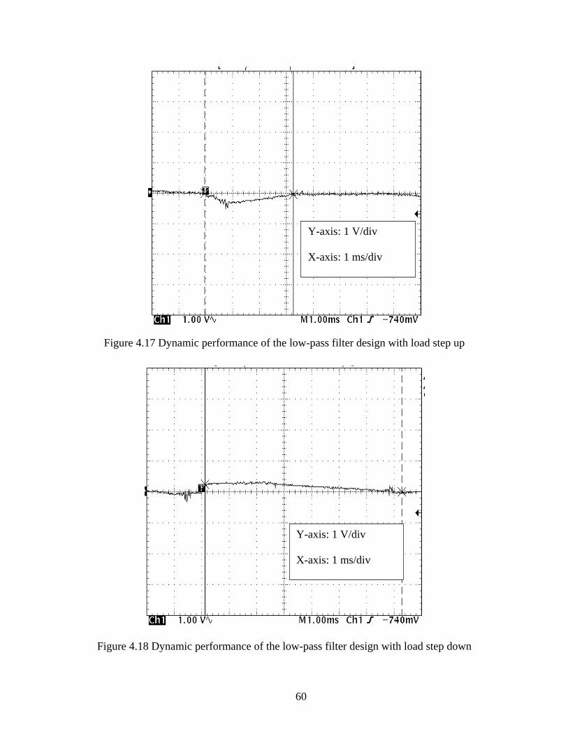
60
Figure 4.17 Dynamic performance of the low-pass filter design with load step up
Figure 4.18 Dynamic performance of the low-pass filter design with load step down
Y-axis: 1 V/div
X-axis: 1 ms/div
Y-axis: 1 V/div
X-axis: 1 ms/div

61
Figure 4.19 Dynamic performance of the slope midpoint design with load step up
Figure 4.20 . Dynamic performance of the slope midpoint design with load step down
Y-axis: 1 V/div
X-axis: 1 ms/div
Y-axis: 1 V/div
X-axis: 1 ms/div

62
CHAPTER 5. I2 AVERAGE CURRENT MODE CONTROL
I2 average current mode control is a new control technique featuring fast dynamic response,
cycle-by-cycle current limiting and accurate current control. It can be treated as peak current mode
control with no peak-to-average error. By combining direct current feedback and average current
feedback, I2 average current mode control is a three loop control system. Since it is a new control
technique proposed in 2013 [6], few papers exist which discuss the small-signal model of this
control method. In this chapter, a small-signal model for I2 average current mode control is
proposed which successfully predicts the sub-harmonics oscillation when the duty cycle is close
to, or greater than, 0.5. The characteristics of I2 average current mode control are also compared
with average current mode control and peak current mode control to show its advantages.
5-1. Introduction
Current mode control for switch-mode power supplies (SMPS) has been a favorite option
for many engineers. The first proposed current control technique, peak current mode control
(PCM), has been widely used in low to medium power applications due to simplification of the
control loop design, cycle-by-cycle current limiting, and prevention of transformer/inductor flux
imbalance [4][41]. Since the inner current loop determines the duty ratio for the active switch in
the converter by using the peak value of the inductor current, the peak-to-average error makes
PCM lose the ability to control the current precisely [37]. For applications where a current source
is preferred, like an LED driver or a battery charger, PCM can barely have zero DC error in the

63
inductor current. As a result, average current mode control (ACM) is used instead of PCM
[30][32]. Compared to PCM, a PI controller is utilized in the current loop in ACM to provide
infinite DC gain. A high frequency pole in the current loop controller impairs the current loop
stability; therefore, a pure PI compensator is recommended [42]. As a result, the ripple in the
inductor current still appears on the output of the current loop compensator while retaining the
shape of the original waveform. However, the PI controller narrows the bandwidth of the current
loop slowing the transient response.
Engineers have attempted to use PCM and ACM simultaneously to obtain both fast
dynamic performance and zero DC error. A new control technique based on this same idea was
proposed in the 2013 [6] and is referred to as I2 average current mode control. The current loop
uses the inductor current signal twice – an average signal calculated by a PI controller and the
peak/valley signal without modification. These two signals determine the duty ratio of the active
switch in the same manner as the voltage signals in V2 control [43]. As shown by the red line in
Figure 5.1, the PI compensator produces the average current signal, which is compared to the
current command. This loop with the PI compensator is designated as a slow loop, which makes
the inductor work as a current source with zero DC error. The peak/valley current signal, shown
by the blue line in Figure 5.1, is directly fed back without delay. As a result, this loop is referred
to as the fast loop, which ensures current limiting and fast dynamic performance. The green line
is the outer voltage loop, which determines the current command to keep the output voltage
constant.
Compared to the traditional current mode control, I2 average current mode control has three
loops instead of two. The modeling of this technique is more complicated than the other current
control methods. The authors of [6] used describing functions to derive the s-domain transfer

64
function by integrating several circuits into a functional block. This procedure yields little insight
into the current loop and the cause of sub-harmonic oscillations. In this chapter, I2 average current
mode control is analyzed in detail, and a small-signal model is proposed. An explanation for the
sub-harmonic oscillations is developed using this model, which is verified by both simulation and
experiment.
5-2. I2 Average Current Mode Control
A constant frequency trailing edge modulated I2 average current mode controlled buck
converter is shown in the Figure 5.1. The inductor current is used twice to determine the switch
duty ratio. The waveforms for the current loop are shown in the Figure 5.2. A pure PI controller is
utilized, because its delay is much less than that of an integral lead-lag compensator. A reference
change in the current propagates through the current loop controller and appears at the output Vi.
Figure 5.1 I2 average current mode control

65
The switch is turned on at the beginning of each cycle by the system clock and turns off at the
instance the inductor current reaches Vi; therefore, the inductor current works as the slope
modulator. In I2 control, both the average value and peak value of the inductor current are utilized,
which in turn provides accurate current control and cycle-by-cycle adjustment. As a result, I2
average current mode control can be treated as a mixture of PCM and ACM, which combines the
advantages of the two control methods. To illustrate the characteristics of I2 average current mode
control, the current waveforms for ACM and PCM are also shown in Figure 5.3. By comparing
the current waveforms in Figure 5.2 and Figure 5.3, traditional PCM and ACM have a tradeoff
between speed and accuracy; however, I2 average current mode control maintains both fast
dynamics and precise control.
Figure 5.2 Current waveforms for I2 ACM control current

66
5-3. Small Signal Modeling
The circuit in Figure 5.1 has 3 loops: a fast loop shown in blue line, a slow loop in red and
a voltage loop in green. In the analysis of the current loop, assume that the voltage loop is open.
Ignoring the slow loop, the fast loop forms a control circuit that looks like that of PCM. By ignoring
the fast loop, the slow loop is similar to ACM. Hence, I2 average current mode control can be taken
as a control system with a current loop having a PCM circuit and an ACM circuit in parallel. The
corresponding small-signal model is shown in Figure 5.4, where Gvd - the duty cycle-to-output
voltage transfer function [44], Gid - duty cycle-to-inductor current transfer function [5], Gvg-the
input-to-output voltage transfer function, Gig-the input-to-inductor current transfer function, Zout –
the output impedance of the power stage, GiL – the transfer function from load current to inductor
current, Gc - the compensator in the voltage loop, Gci - the controller in the current loop, Fm - the
modulator gain, Ri – the current sense resistor, He - the sampling gain, Vref - the voltage reference,
Vo - the output voltage, IL - the inductor current, Ic - the current reference, Vi - the slow loop current
Figure 5.3 Waveforms for ACM and PCM control

67
compensator output, and d - the duty cycle applied to the switch. Normally, the feed-forward gains
kf and kr are small, have little effect on the current loop gain, and can be ignored in the early stage
analysis.
Although there is an integrator in the current loop, the gain (1+Gci(s)) in the forward path
transmits the change in the current reference without delay. The current ripple, which is utilized
Figure 5.4 Small-signal model for I2 ACM control

68
instead of a constant external ramp to determine the duty ratio, contains the circuit operating
information and makes the transient response faster.
It should be noted that the modulator gain Fm in this control technique is different from
those of PCM and ACM; an expression for this gain will be derived later. The gains kr and kf for
the input and output voltage are typically found in PCM and ACM models; however, they are also
different from those utilized in the traditional control methods due to the two current loops.
5-3-1. Modulator Gain
For the current compensator in Figure 5.5, the s-domain transfer function is
𝐺𝑐𝑖(𝑠) =𝑘𝑐𝑖∙(1+𝑠/𝜔𝑧𝑐𝑖)
𝑠 (5-1)
where 𝜔𝑧𝑐𝑖 =1
𝐶1∙𝑅2 and 𝑘𝑐𝑖 =
1
𝐶1∙𝑅1.
The phase delay introduced by (1) is
delay = 𝑡𝑎𝑛−1(2𝜋𝑓𝑠𝐶1𝑅2) − 90° (5-2)
where fs is the frequency of the signal being processed. The negative value in (5-2) indicates that
the output of the current compensator is lagging the input. Generally, capacitor C1 and resistor R2
produce a zero located below the resonant frequency of the power stage; thus, the first term in (5-
2) is close to 90⁰. Taking the inverted input into consideration, the current compensator output is
Figure 5.5 Current compensator and modulator

69
similar to the inverted inductor current. Assume that the input signal (the inductor current) has a
rising slope of Sn, the corresponding compensated output signal has the falling slope Snc at the
switch turn-on instant and can be calculated in the following process.
The s-domain transfer function for the inductor current while the switch is turning on can
be written as
𝐼𝐿(s) =𝑆𝑛
𝑠2 (5-3)
the output of the current compensator is expressed as
𝑉𝑖(s) = −𝐺𝑐𝑖(𝑠) ∙ 𝐼𝐿(𝑠) = −𝑆𝑛 ∙ 𝑘𝑐𝑖 ∙ (1
𝜔𝑧𝑐𝑖∙𝑠2 +1
𝑠3) (5-4)
where the minus sign is due to the current feeding back to the inverted input of the current
compensator. By using the inverse Laplace transformation, the output in (5-4) can be represented
in time domain as
𝑣𝑖(t) = −𝑆𝑛 ∙ 𝑘𝑐𝑖 ∙ (𝑡
𝜔𝑧𝑐𝑖+
𝑡2
2) (5-5)
Figure 5.6 Current waveforms for modulator

70
Taking the derivative of the (5-5) at the time t=DTs, the result is
𝑆𝑛𝑐 = −𝑆𝑛 ∙ 𝑘𝑐𝑖(𝐷𝑇𝑠 + 1/𝜔𝑐𝑖) (5-6)
It can be noticed from (5-6) that Snc varies with the duty ratio and the current loop compensator
design; therefore, the overall modulator gain varies with operating point.
With the slope of the inductor current and the current compensator output, the waveforms
which describe the modulation are shown in Figure 5.6. The variables <Vi> and <Ri*IL> indicate
the average value in a cycle, which are marked by dashed lines. Since the angle calculated from
(5-2) is close to zero in most cases, the delay introduced by the PI controller can be safely
approximated as 180 degrees. Therefore, (5-7) is satisfied during steady state operation. Since the
waveforms of the fast loop and the slow loop are both changing in a cycle, the absolute slope for
the modulation is related to the difference between the slopes of the two current waveforms.
< 𝑉𝑖 >=< 𝑅𝑖 ∙ 𝐼𝐿 > +1
2𝐷𝑇𝑠(𝑆𝑛 − 𝑆𝑛𝑐) (5-7)
Perturb the inductor current while keeping the other parameters fixed to obtain the
modulator gain, Fm1, of the fast loop [5].
𝐹𝑚1 =
<𝑅𝑖𝐼>= −
2
(𝑆𝑛+𝑆𝑛𝑐)∙𝑇𝑠 (5-8)
A similar methodology can be used to derive the modulator gain, Fm2, in the slow loop.
𝐹𝑚2 =
<𝑉>=
2
(𝑆𝑛+𝑆𝑛𝑐)∙𝑇𝑠 (5-9)
It turns out the modulator gains seen by the fast loop and slow loop have the same magnitude but
are different in sign. Therefore, a unified modulator gain Fm is used in the model of Figure 5.4,
which is the same as (5-9).
𝐹𝑚 =
<𝑉>=
2
(𝑆𝑛+𝑆𝑛𝑐)∙𝑇𝑠 (5-10)

71
As a common problem of ripple based control methods [45] like peak current mode control
and V2 control, I2 average current mode control also suffers from “sub-harmonic oscillation” when
the duty ratio is close to or greater than 0.5. An artificial slope can be used to decrease the
modulator gain to stabilize the current loop. If a ramp of slope Se is needed, then (5-10) becomes
𝐹𝑚 =
<𝑉>=
2
(𝑆𝑛+𝑆𝑛𝑐+𝑆𝑒)∙𝑇𝑠 (5-11)
If slope compensation is added through a voltage divider, the dividing ratio should also be applied
to the current sense resistor of the fast loop, which makes it different from that of the slow loop.
5-3-2. Sampling Gain
I2 average current mode control uses the ripple of the inductor current in the same way as
PCM in the fast loop. The current loop for PCM operates as a sampling system instead of averaged
state feedback. By the same derivation process in [4], the fast loop of I2 average current mode
control turns out to have the same sampling gain
𝐻𝑒(𝑠) ≈ 1 +𝑠
𝜔𝑛𝑄𝑧+
𝑠2
𝜔𝑛2 (5-12)
where 𝑄𝑧 =−2
𝜋, and 𝜔𝑛 =
𝜋
𝑇𝑠.
The phenomenon, “sub-harmonic oscillation”, is mainly due to (5-12), which has two RHP
zeroes at half of the switching frequency. Note that this model is only accurate up to half the
switching frequency due to approximations.
It should be mentioned that (5-12) is an approximation valid only for constant frequency
operation. However, for the variable frequency operation like constant on-time control, (5-12) fails
to describe the sampling effect [46].

72
Due to the PI controller in the slow loop, the output contains the average signal for the
inductor current; therefore, the slow loop is true state feedback [31] and the sampling gain from
(5-12) is not shown in the slow loop as depicted in Figure 5.4.
5-3-3. Feedback and Feed-forward Gain
The small-signal model for peak current mode control has been studied for over three
decades. The feed-forward gain from the input voltage to the inductor current and the feedback
gain from the output voltage to the inductor current were fully developed in [4], which is based on
a simplified current cell common to all converters. The corresponding derived gains are shown
below
𝐾𝑓_𝑓𝑙′ = −
𝐷𝑇𝑠𝑅𝑖
𝐿(1 −
𝐷
2) (5-13)
𝐾𝑟_𝑓𝑙′ =
𝐷′2𝑇𝑠𝑅𝑖
2𝐿 (5-14)
where 𝐾𝑓_𝑓𝑙′ is the feed-forward gain and 𝐾𝑟_𝑓𝑙
′ is the feedback gain for the invariant current cell in
peak current mode control. For different converter topologies, the corresponding feed-forward gain
and feedback gain are the combination of (5-13) and (5-14) related to the existence of the input
and output voltage during the turn on and turn off time.
Since the fast loop in the I2 average current mode control works in the same manner as for
PCM, the perturbations of input and output voltages have the same effect on the inductor current
as proved in [4] through the fast loop.
Although there is a current compensator in the slow loop, the inductor current ripple still
appears at the output, because a PI controller is used which has less damping than that of a type II
compensator. The feed-forward and feedback effect in the slow loop will be modified by the
current compensator as shown in (5-15) and (5-16).

73
𝐾𝑓_𝑠𝑙′ = 𝐾𝑓_𝑓𝑙
′ ∙ 𝐺𝑐𝑖 (5-15)
𝐾𝑟_𝑠𝑙′ = 𝐾𝑟_𝑓𝑙
′ ∙ 𝐺𝑐𝑖 (5-16)
As discussed in the modulator gain section, the PI controller contributes a phase delay close
to 180 degrees, which can be approximated as an inverted input signal with magnitude
magnification at the switching frequency.
𝐾𝑓_𝑠𝑙′ = −𝐾𝑓_𝑓𝑙
′ ∙ |𝐺𝑐𝑖|𝑓=𝑓𝑠 (5-17)
𝐾𝑟_𝑠𝑙′ = −𝐾𝑟_𝑓𝑙
′ ∙ |𝐺𝑐𝑖|𝑓=𝑓𝑠 (5-18)
Based on (5-15)-(5-18), the total feed-forward and feedback gains in I2 average current mode
control are
𝐾𝑓′ = 𝐾𝑓_𝑓𝑙
′ − 𝐾𝑓𝑠𝑙
′ = (1 + |𝐺𝑐𝑖|𝑓=𝑓𝑠) ∙ [−
𝐷𝑇𝑠𝑅𝑖
𝐿(1 −
𝐷
2)] (5-19)
𝐾𝑟′ = 𝐾𝑟_𝑓𝑙
′ − 𝐾𝑟_𝑠𝑙′ = (1 + |𝐺𝑐𝑖|𝑓=𝑓𝑠
) ∙𝐷′2𝑇𝑠𝑅𝑖
2𝐿 (5-20)
As stated in [2], the expressions of (5-19) and (5-20) are derived from the invariant current
cell, the gains 𝐾𝑓′ and 𝐾𝑟
′ are the effects on the inductor current from on-time voltage and off-time
voltage across the inductor respectively. Since the on-time voltage and off-time voltage are linear
combinations of input voltage and output voltage, the feedforward gain 𝐾𝑓 from the input voltage
and feedback gain 𝐾𝑟 from output voltage can be also represented as the linear combinations of
the 𝐾𝑓′ and 𝐾𝑟
′. Take the buck converter as an example, the on-time voltage is 𝑉𝑔 − 𝑉𝑜, the input
voltage 𝑉𝑔 and output voltage −𝑉𝑜 affects the inductor current through the transfer function 𝐾𝑓′.
The off-time voltage is 𝑉𝑜, which affects the inductor current through the gain 𝐾𝑟′. As a result, the
feedforward gain 𝐾𝑓 from the input voltage is 𝐾𝑓′, the feedback gain 𝐾𝑟 from the output voltage is
−𝐾𝑓′ + 𝐾𝑟
′. The feedforward gain and feedback gain in terms of 𝐾𝑓′ and 𝐾𝑟
′ for three basic DC-DC
converters are collected in Table 5-1.

74
Table 5-1 Feedforward Gain and Feedback Gain as a Representation of 𝐾𝑓′ and 𝐾𝑟
′
Buck Boost Buck-Boost
𝐾𝑓 𝐾𝑓′ 𝐾𝑓
′ − 𝐾𝑟′ 𝐾𝑓
′
𝐾𝑟 −𝐾𝑓′ + 𝐾𝑟
′ 𝐾𝑟′ 𝐾𝑟
′
5-4. Transfer Function Characteristics
The small-signal model developed in the previous section introduces insight into the
advantages of I2 average current mode control. To illustrate the characteristics of fast dynamics
and accuracy, the I2 average current mode control is compared with traditional average current
mode control and peak current mode control.
A buck converter was used to perform this comparison. The frequency responses of the
control-to-output voltage, the current loop, audio-susceptibility and the output impedance were
checked. Stability analysis was also performed. The circuit parameters for the converter prototype
are collected in the table below.
Table 5-2 Circuit Parameters for the Prototype Converter
Para. Value Para. Value Para. Value Para. Value
Vg 5 V Vo (V) 3 V Ts 10 µs fs 100 kHz
L 20.78 µH RL 0.353 Ω C 318 µF Rc 0.169 Ω
Rs 0.065 Ω Acl 10 Ri = Rs*Acl 0.65 Ω R 2.8 Ω
Se 0.1V/us Fm_av 1/1.8 iso_gain 1/3 R1 15 kΩ
R2 15 kΩ C1 5500 pF

75
where Rs is the resistor inserted in series with the inductor to sample the current, Acl is the current
sense gain, Ri is the equivalent sense resistor in the model, and Rl is the equivalent resistor of
inductor.
Since the steady state duty ratio is greater than 0.5, an external ramp Se is added into the
modulation in I2 control and PCM. This value is used throughout this section, except for Figure
5.11 and Figure 5.12. The modulator gain used for ACM is Fm_av , which is a common value for
most PWM control chips. The iso_gain indicates the dividing ratio from the current controller to
the comparator, which can be multiplied into (5-1) or (5-11). The parameters R1, R2 and C1 are the
components used to form the current controller in Figure 5.5, which is used for both I2 control and
ACM.
Figure 5.7 Current loop transfer functions

76
5-4-1. Current Loop Gain
Referring to Figure 5.4, the current loop gain is the transfer function with the voltage loop
open and can be expressed by the following for I2 control
𝑇𝑖𝑖 = 𝐺𝑖𝑑 ∙ 𝐹𝑚 ∙ 𝑅𝑖(𝐺𝑐𝑖 + 𝐻𝑒) (5-21)
The transfer function is compared with that of PCM and ACM in Figure 5.7. With the
voltage loop open, I2 control and ACM behave as an ideal current source at low frequencies. In
comparison, PCM has much less low frequency gain, which results in DC current error. It is shown
that I2 average current mode control increases both the current loop gain and the phase margin. As
a result, I2 control has both fast tracking speed and little overshoot.
Figure 5.8 Control-to-output transfer functions

77
5-4-2. Control-to-output Voltage
When the voltage loop is closed, the transfer function from the voltage controller output to
output voltage for I2 control can be calculated by Mason’s gain rule from Figure 5.4,
𝐺𝑣𝑐 =(1+𝐺𝑐𝑖)∙𝐹𝑚∙𝐺𝑣𝑑
1+𝑇𝑖𝑖−𝐾𝑟∙𝐹𝑚∙𝐺𝑣𝑑 (5-22)
Figure 5.8 Control-to-output transfer functions is a comparison of the three current control
methods. As can be seen, I2 control behaves like ACM in the low frequency range and PCM in the
mid-range frequency, which behaves like a first order system. The peaking at half the switching
frequency indicates a pair of double poles, which need to be damped by an artificial ramp.
5-4-3. Audio Susceptibility
The closed loop audio susceptibility is defined as the transfer function of the input-to-
output voltage with closed current loops and an open voltage loop. Because of the different
frequency response of the current loops of I2 ACM control, PCM and ACM, the effect of voltage
Figure 5.9 Comparison of audio susceptibility

78
loop compensators are ignored to reveal the effect of current loops. The audio-susceptibility of I2
ACM control can be solved by a set of equations developed from Figure 5.4. Due to the open
voltage loop, the current command 𝐼 is zero here.
𝑉 = 𝑉𝐺𝑣𝑔 + d𝐺𝑣𝑑 − 𝐼𝑍𝑜𝑢𝑡
d = 𝐹𝑚[𝑉𝑘𝑓 + 𝑉𝑘𝑟 − 𝐼(𝐻𝑒 + 𝐺𝑐𝑖)𝑅𝑖]
𝐼 = 𝑉𝐺𝑖𝑔 + 𝐺𝑖𝑑 + 𝐼𝐺𝑖𝐿 (5-23)
For deriving the audio-susceptibility transfer function, the output current is assumed to be
constant. Therefore, the small-signal variable 𝐼 = 0. The resulting transfer function is
𝑉
𝑉=
𝐺𝑣𝑔(1+𝑇𝑖𝑖)+𝐹𝑚∙𝐺𝑣𝑑[𝐾𝑓−𝐺𝑖𝑔(𝐻𝑒+𝐺𝑐𝑖)𝑅𝑖]
1+𝑇𝑖𝑖−𝐾𝑟∙𝐹𝑚∙𝐺𝑣𝑑 (5-24)
The comparison of the audio susceptibilities under these control techniques can be seen from
Figure 5.9. It is obvious that the audio-susceptibility is improved significantly with I2 control, which
has the lowest magnitude in the low frequency range. PCM is the most sensitive control method in
this case, because of the higher magnitude at low frequencies. To include the effect of the voltage
loop compensator, which is not discussed here, the variation from the voltage loop can be written
into the duty ratio expression in (5-23), then solved for the desired transfer function.
5-4-4. Output Impedance
The output impedance indicates the output voltage drop during load change, which is also
modified by the control method. The output impedance shown here is developed with current loops
closed and voltage loop open. Using the set of equations (5-23) and setting the variable 𝑉𝑔 = 0 , the
output impedance can be represented as
𝑉
−𝐼=
𝑍𝑜𝑢𝑡(1+𝑇𝑖𝑖)+𝐺𝑣𝑔𝐹𝑚𝐺𝑖𝐿(𝐻𝑒+𝐺𝑐𝑖)𝑅𝑖
1+𝑇𝑖𝑖−𝐾𝑟∙𝐹𝑚∙𝐺𝑣𝑑 (5-25)

79
It can be seen in Figure 5.10 that output impedances for the three control methods have similar
curvature and close values above half the switching frequency. Since the current loops have fairly
low gain at high frequency, the characteristics of the power stage impedance will be the dominant
factor. Below half the switching frequency, I2 ACM has the lowest output impedance, which makes
it an excellent solution for applications having frequent load change.
5-4-5. Stability
It is of great interest to know whether I2 control is stable and if slope compensation is
needed. Adding an external slope decreases the loop gain, reduces the bandwidth, and slows down
the transient speed. Let’s define a parameter
𝑚𝑐 =𝑆𝑒
𝑆𝑛 (5-26)
Figure 5.10 Comparison of output impedance

80
Figure 5.12 Control-to-output voltage for different mc for a 2 V output
Figure 5.11 Control-to-output voltage for different mc for a 3 V output

81
Figure 5.11 shows the control-to-output voltage transfer function with mc as a variable.
When mc = 0, the magnitude peak and phase increase at half the switching frequency, indicating a
pair of right half plane poles, which is the reason for the system being unstable. For I2 average
current mode control, the control loop still suffers oscillation without slope compensation, even
when the duty ratio is down to 0.4. Figure 5.12 shows the results when the nominal output voltage
was decreased to 2 V. The magnitude peak at half the switching frequency goes through 0 dB and
causes a second crossover as commonly seen in PCM. This same phenomenon happens when mc
= 1 in Figure 5.12. Slope compensation can help to damp the peaking and move the RHP poles
into the left half plane.
5-5. Simulation and Experimental Verification
The same buck converter with a 2 V output in previous section was used as an example to
compare the frequency response of the model as plotted with MATLAB versus simulation results
from Simplis. Experimental measurements using an AP300 network analyzer from Ridley
Engineering were also obtained. With a 5 V input and a 2 V output, the circuit still suffered from
the sub-harmonic oscillation as illustrated in Figure 5.11. Therefore, the input voltage was selected
to vary from 3.3 V to 6 V, the steady state duty cycle is from 0.33 to 0.606.
5-5-1. Simulation Results
The first simulation was performed to verify the validation of the most inner current loop
model with both the voltage loop and the slow current loop open. Thus, the current compensator
output 𝑉 = 0. The corresponding transfer function is given as
𝐺𝑖_𝑓𝑙 =𝐹𝑚∙𝐺𝑣𝑑
1+𝑇𝑖−𝐾𝑟_𝑓𝑙∙𝐹𝑚∙𝐺𝑣𝑑 (5-27)
where 𝑇𝑖 = 𝐹𝑚 ∙ 𝐺𝑖𝑑 ∙ 𝑅𝑖 ∙ 𝐻𝑒 is the open loop transfer function of the most inner current loop.
Since the slow loop was kept open, the feedback gain 𝐾𝑟_𝑠𝑙 is not taken into consideration. With

82
only the fast loop closed, the circuit behaves in the same way as PCM which determines the duty
ratio using only the slope of the inductor current. As seen from Figure 5.13 and Figure 5.15, the
model prediction matches very well with the simulation results from Simplis.
The second test was to verify the accuracy of (5-22). In Figure 5.14, the difference in the
mid-range is mainly due to the non-ideal operational amplifier of the current controller used in the
simulations [6]. The reason behind picking (5-22) and (5-27) is that these two transfer functions
can be measured with a network analyzer; therefore, the simulation results can be verified with
measurements. With the model confirmation for I2 control operating with slope compensation, it
is also of interest to check the performance of the control technique without the external slope. To
stabilize the circuit without the help of slope compensation, the input voltage was increased to 6
V to decrease the duty ratio. The same comparison between the model prediction and simulation
Figure 5.13 Model prediction and simulation results for equation (5-27) with 5 V input

83
results are shown in Figure 5.15 and Figure 5.16. It can be seen that the model predictions are very
close to the simulation results. The magnitude and phase deviations around half the switching
frequency are mainly due to the non-ideal operational amplifier used in the simulation. The limited
bandwidth causes current slope distortion at the output of the current loop controller and results in
a high quality factor peaking at half the switching frequency [6].
Figure 5.14 Model prediction and simulation results for equation (5-22) with 5 V input

84
Figure 5.15 Model prediction and simulation result for (5-27) with a 6 V input
Figure 5.16 Model prediction and simulation result for (5-22) with a 6 V input

85
5-5-2. Experimental Results
To further verify the modeling discussed, a prototype buck converter was constructed using
a TI UCC38C40 and an LF347 quad operational amplifier. The schematic of the overall system is
shown in Figure 5.17. Since there are three control loops, the voltage loop and slow loop were
implemented using op amps 1 and 2, respectively. Op amp 3 was programmed as a current sense
amplifier with gain of 10. Finally, op amp 4 was connected as a voltage follower and utilized in
the slope compensation circuit. The slope compensation is generated from the switch gate driver
signal [47], which keeps the circuit working in the constant frequency mode. The slope
compensated inductor current signal was fed into the negative input of the comparator on the
UCC38C40. It should be noted that there is a gain of 1/3 between the comp pin and the positive
Figure 5.17 Schematic of the buck converter prototype

86
input of the comparator. Thus, the output of op amp 2 was scaled and compared with the inductor
current peak signal.
The frequency responses were measured using the AP300 network analyzer. The measurements
from point a to point c in Figure 5.17 correspond to the results of (5-22). To measure the transfer
function of (5-27), the voltage loop and slow loop were open, a voltage source is connected at point
b to provide the DC bias voltage.
In experimental tests, the input voltage was selected as 3.3 V, 5 V and 6 V, as shown in
Figure 5.18 through Figure 5.25. For the 6 V input, the frequency response was measured with and
without slope compensation. Since the signal beyond half the switching frequency was noisy and
distorted, the comparison of the model and measurement was conducted in the range from 10 Hz
to half the switching frequency. As can be seen from Figure 5.18 to Figure 5.25, the proposed
model matches the measurement very well. It should be noted that the magnitude dip in the
measurement of control-to-output voltage transfer function is smaller than 2dB, which was also
reported in [32].
5-6. Conclusion
I2 average current mode control is a promising technique which provides the advantages of
fast dynamic speed and precise current control. The current loop uses the both the average current
signal and the peak current value to determine the PWM output; therefore, an ideal current source
with cycle-by-cycle current limiting is achieved.
Because of the existence of three control loops, the analysis of I2 average current mode
control is more complicated than the traditional current mode control methods. In this chapter, the
I2 average current mode control is taken as a combination of average current control and peak
current control and analyzed loop by loop. The small-signal characteristics of this control

87
technique were compared with ACM and PCM, which revealed the advantages of I2 control. The
large low-frequency gain and bandwidth confirms that I2 average current mode control is fast and
accurate. The complex poles at half the switching frequency will move into the right half plane
when the duty ratio is close to, or greater than, 0.5. The resonant peak produced by these poles
would cause a second crossover, even with the duty ratio down to 0.4. An external slope can be
added to the sensed inductor peak current to move the poles into the left half plane and damp the
resonant peak.
The model proposed here for I2 average current mode control was confirmed with
simulation results from Simplis and measurements with an AP300 network analyzer. The
frequency responses predicted by the proposed model for the inner current loop and control-to-
output voltage matched those obtained from Simplis and measurements. As a result, the proposed
model is useful in the design of current loop and voltage loop compensators for I2 average current
mode controllers.

88
Figure 5.19 Measurement of inner current loop for a 5 V input
Figure 5.18 Measurement of inner current loop for a 3.3 V input

89
Figure 5.20 Measurement of inner current loop for a 6 V input
Figure 5.21 Measurement of inner current loop for a 6 V input and no slope compensation

90
Figure 5.22 Measurement of control-to-output voltage for a 3.3 V input
Figure 5.23 Measurement of control-to-output voltage for a 5 V input

91
Figure 5.25 Measurement of control-to-output voltage for a 6 V input and no slope compensation
Figure 5.24 Measurement of control-to-output voltage for a 6 V input

92
CHAPTER 6. DIGITAL I2 AVERAGE CURRENT MODE CONTROL
I2 average current mode control was introduced in the Chapter 5, which has three control
loops in an analog implementation. Therefore, the analysis of this analog control method is more
complicated than the other current mode control techniques. By implementing this technique
digitally, the number of control loops is reduced, and the complexity of the loop design is
simplified. In this chapter, the digital control law, which only requires sampling the inductor
current once in a cycle, is developed by using the predictive current mode control introduced in
Chapter 2 and digital average current mode control in Chapter 4. A small-signal model for this
control technique is also proposed. Simulation results show that it has a faster transient response
than average current mode control while keeping zero DC current error. Experimental results
demonstrate the characteristics of this digital implementation of I2 average current mode control
and verify the accuracy of the proposed small-signal model.
6-1. Introduction
I2 average current mode control, introduced in Chapter 5, uses both the instantaneous value
and average signal. It is hard for digital units to sense these signals, especially in high frequency
operation. This chapter is focused on how to implement I2 average current mode control using a
digital processor
As a review, I2 average current mode control has the advantages of both fast dynamic
response and zero DC current error. The control circuit uses the current signal twice in two current
loops, one with an integrator called the slow loop and one with direct current feedback called the

93
fast loop. Thus, this method is characterized by three control loops – a slow loop, a fast loop and
a voltage loop - making its analysis and design much more complicated than PCM and ACM.
The goal of this chapter is to introduce a digital implementation of I2 average current mode
control. This implementation reduces the number of control loops, because the duty ratio is
determined by predicting the inductor current slope and the peak value of the current ripple. Thus,
this digital implementation yields I2 average current mode control with less complexity than an
analog implementation while maintaining its advantages.
Shown in Figure 6.1 is a constant frequency trailing edge I2 average current mode
controlled boost converter. Note that the inductor current signal is used twice to determine the
duty ratio. There is a slow loop, marked in red, containing a PI controller to produce the average
Figure 6.1 I2 average current mode controlled boost converter

94
value of the inductor current. A fast loop, marked in blue, utilizes the inductor current without
delay. At the beginning of each switching cycle, the active switch is turned on by the system clock
and turned off at the instant when the current ripple reaches the average signal, as illustrated in
Figure 6.2. The PI controller in the slow loop provides infinite DC gain to guarantee perfect
tracking of the current reference. The fast loop utilizes the inductor current slope and valley value,
which eliminates the need for an external ramp for modulation. Therefore, I2 average current mode
control combines the functions of PCM and ACM. This control technique requires three control
loops: fast loop, slow loop and voltage loop, which makes the analysis and design more difficult
than conventional current mode control.
6-2. Digital I2 Average Current Mode Control
A digital controller only processes discrete signals. However, I2 average current mode
control needs to use the instantaneous value of the inductor current to determine the duty ratio.
One solution would be to sample the inductor current N times in a switching cycle and turn off the
active switch when the latest sampled value equals the average value. Using this approach, the
digital controller is very close to an analog controller. The obvious downside is that the clock rate,
Figure 6.2 Current waveforms for analog I2 control

95
fclk, for the digital system has to be equal to or greater than N times the switching frequency, fs,
thus increasing the cost of the controller. Also, if the digital controller cannot sample the inductor
current and calculate the output signal in the same switching period, there will be at least a two
cycle delay, because the sampling and calculations will occur in two consecutive switching cycles.
The digital implementation proposed here only utilizes one sample of the inductor current
in a switching cycle and predicts the time required for the inductor current to reach its average
value. Consider the PI compensator at the bottom of Figure 6.1. The inductor current is fed back
to the inverted input of the operational amplifier in this compensator. The output signal Vi, as
marked in red in Figure 6.2, looks like the inverted inductor current with a phase delay introduced
by the PI controller. Ignoring this delay, which is generally very small, the switching instant is at
the inductor current peak value corresponding to the valley value of Vi. Thus, the digital controller
only needs the peak value of the current ripple, Ipeak, which can be acquired in only one sample in
a switching cycle.
6-2-1. Current Loop Compensator
In the model of analog ACM [30], the current loop compensator gain is (1+Gci(s)) where
Gci(s) is in the current feedback path and is the s-domain transfer function of the compensator
Figure 6.3 Perturbation in digital I2 control signal

96
looking into its inverted input. Therefore, calculations for the current reference signal and the
inductor current feedback signal must be performed in parallel, which is inefficient for digital
processors. For digital average current mode control, the processor can utilize the error between
the discretized reference signal and the sampled value to compute the output command in one
calculation as shown in (6-1), which saves processing power and time.
𝑒𝑖 = 𝑅𝑖 ∙ 𝐼𝑐𝑝𝑒𝑎𝑘 − 𝑅𝑖 ∙ 𝐼𝑝𝑒𝑎𝑘 (6-1)
In this equation, ei is the error between the current reference and the sampled current signal, Icpeak
is the peak value of the voltage loop compensator output signal, Ipeak is the peak value of the
inductor current sample, and Ri is the current sense resistor.
After calculating the error signal, a discrete difference equation Gci(z), which is the z-
domain transfer function of Gci(s), is utilized to calculate Vi as shown in (6-2). Gci(s) will be
designed in the s domain and then Gci(z) will be generated using the Bilinear transformation.
𝑉𝑖 = 𝐺𝑐𝑖(𝑧) ∙ 𝑒𝑖 + 𝐼𝑐𝑝𝑒𝑎𝑘 ∙ 𝑅𝑖 (6-2)
The quantity Icpeak in (6-2) is used to offset the voltage Vi, because the current limiting
signal should not be zero but equal to the inductor peak current when the current error signal ei is
zero.
6-2-2. Modulator
Since the digital controller utilizes discrete quantities, the output signal is constant in a
cycle. As shown in Figure 6.3, an exaggerated perturbation, indicated by two black dashed lines,
occurs in the nth cycle. Assume that the peak value of the current ripple is Ipeak, the rising slope of
the inductor current is Sn and falling slope is Sf. The difference between the current ripple peak
and the current compensator output signal e is given by (6-3)
e[n] = 𝑉𝑖[𝑛] − 𝐼𝑝𝑒𝑎𝑘[𝑛] ∙ 𝑅𝑖 (6-3)

97
where [n] indicates the nth cycle. The change in peak inductor current ∆Ipeak corresponding to a
change ∆d in the duty ratio for all three basic dc-dc converters (buck, boost, buck-boost) is
∆𝐼𝑝𝑒𝑎𝑘 = (𝑆𝑛 + 𝑆𝑓) ∙ ∆𝑑 ∙ 𝑇𝑠 (6-4)
∆d =∆𝐼𝑝𝑒𝑎𝑘
(𝑆𝑛+𝑆𝑓)∙𝑇𝑠 (6-5)
Therefore, the adjustment of the duty ratio which ensures that the peak current of the (n+1)th cycle
equals Vi is
d[n + 1] = 𝐷𝑠𝑠 +𝑒[𝑛]
(𝑆𝑛+𝑆𝑓)∙𝑇𝑠 (6-6)
Inserting (6-1), (6-2) and (6-3) into (6-6) yields (6-7),where Dss is the duty ratio in steady
state, which could also be calculated by the steady state inductor current rising slope Snss and falling
slope Sfss
d[n + 1] = 𝐷𝑠𝑠 +(1+𝐺𝑐𝑖(𝑧))∙𝑒𝑖
(𝑆𝑛+𝑆𝑓)∙𝑇𝑠 (6-7)
𝐷𝑠𝑠 =𝑆𝑓𝑠𝑠
𝑆𝑛𝑠𝑠+𝑆𝑓𝑠𝑠 (6-8)
Using the ideal Dss in (6-6) instead of the actual duty ratio reduces the computation time
required by (6-7) and enables high frequency operation, but an error between Dss and the real duty
ratio increases the time required to reach the new operating point.
A common problem of ripple based control methods, such as peak current mode control
and V2 control, is “sub-harmonic oscillation”. I2 average current mode control also suffers from
“sub-harmonic oscillation” when the duty ratio is close to or greater than 0.5. With the digital
modulation expression of (6-7), an external ramp can be easily added to the modulator. If a ramp
of slope Se is needed, then (6-7) becomes
d[n + 1] = 𝐷𝑠𝑠 +(1+𝐺𝑐𝑖(𝑧))∙𝑒𝑖
(𝑆𝑛+𝑆𝑓+𝑆𝑒)∙𝑇𝑠 (6-9)

98
Since Dss is constant and (1+Gci(z)) is the transfer function of the current loop compensator, the
gain Fm of (6-9) is
𝐹𝑚 =1
(𝑆𝑛+𝑆𝑓+𝑆𝑒)∙𝑇𝑠 (6-10)
The modulator gains in terms of converter input voltage Vg and output voltage Vo for three
basic dc-dc converters are shown in Table 6-1.
Table 6-1 Modulator Gain for Basic Topologies
Topology Fm
Buck 1
(𝑉𝑖𝑛
𝐿+ 𝑆𝑒)𝑇𝑠
Boost 1
(2𝑉𝑖𝑛 − 𝑉𝑜
𝐿+ 𝑆𝑒)𝑇𝑠
Buck-Boost 1
(𝑉𝑖𝑛 + 𝑉𝑜
𝐿+ 𝑆𝑒)𝑇𝑠
6-3. Small-Signal Model and Design Guideline
Unlike analog I2 average current mode control, the digital implementation integrates the
fast loop into the modulator calculating the duty ratio. Hence, digital I2 average current mode
control is a two loop control system, which reduces the complexity of the loop design. In Figure
6.4, the small-signal model for digital I2 average current mode control is provided, where Gvd is
the duty cycle-to-output voltage transfer function, Gid the duty cycle-to-inductor current transfer
function, Gc the compensator in the voltage loop, Gci the controller in the current loop, Fm the
modulator gain, He the sampling gain [4], Hc the computation and PWM update delay, zero order
hold(ZOH) the transfer function of the digital pulse-width-modulation, Vref the voltage reference,

99
Vo the output voltage, IL the inductor current, Vc the current reference, ei the current error, and d
the duty cycle applied to the switch. Since the current peak value is used in the current loop, the
sampling gain He, which is the same as that in analog peak current mode control, is also shown in
the current loop here. It should also be noticed that the ZOH introduces extra phase lag, which is
a disadvantage of digital control.
There are two basic approaches for designing the digital controllers: a direct digital design
and an indirect digital design, which begins with an analog design that is transformed to a digital
implementation. Comparing the achievable phase margin and bandwidth of the loop design, direct
digital design has its benefits. However, the indirect digital design can use many well-known
Figure 6.4 Small-signal model of digital I2 current mode control

100
traditional tools developed for analog circuits, thus easing the design work. Here, the indirect
digital design was used to calculate the parameters for the compensators.
6-3-1. Current Loop Compensator
The current loop control-to-inductor current transfer function is
𝑇𝑖 = (1 + 𝐺𝑐𝑖) ∙ 𝐹𝑚 ∙ 𝐻𝑐 ∙ 𝑍𝑂𝐻 ∙ 𝐺𝑖𝑑 ∙ 𝑅𝑖 ∙ 𝐻𝑒 (6-11)
where Gci is a PI controller formed by an integrator and a low frequency zero, which provides
high gain at low frequency and the desired phase margin,
𝐺𝑐𝑖(s) =𝑘𝑐𝑖∙(1+𝑠/𝜔𝑧𝑐𝑖)
𝑠 (6-12)
In this equation, kci is the proportional gain and ωzci is the location of the low frequency
zero. It should be mentioned that (1+Gci(s)) in (6-11) is the block generating the current limiting
signal. After transforming (6-12) by the Bilinear transformation, the discrete difference
representation can be represented by (6-13)
𝐺𝑐𝑖(z) =𝑘𝑐𝑖
2𝜔𝑧𝑐𝑖∙
(𝜔𝑧𝑐𝑖𝑇𝑠+2)∙𝑧+(𝜔𝑧𝑐𝑖𝑇𝑠−2)
𝑧−1 (6-13)
For the concern of loop stability and bandwidth, the low frequency zero is normally placed
below the resonant frequency of the power stage to provide sufficient gain and phase margin.
6-3-2. Voltage Loop Compensator
The voltage loop compensator is the traditional integral lead-lag controller
𝐺𝑐(𝑠) =𝑘𝑐
𝑠
(1+𝑠/𝜔𝑧)
(1+𝑠/𝜔𝑝) (6-14)
where kc is the gain, ωz is the low frequency zero and ωp is the high frequency pole. These values
can be calculated by the K-factor approach to achieve the desirable bandwidth and phase margin.
The discretized representation of (6-14) is

101
𝐺𝑐(𝑧) =𝑇𝑠
2
𝑘𝑐𝜔𝑝
𝜔𝑧
(𝜔𝑧𝑇𝑠+2)𝑧2+2𝜔𝑧𝑇𝑠𝑧+(𝜔𝑧𝑇𝑠−2)
(𝜔𝑝𝑇𝑠+2)𝑧2−4𝑧−(𝜔𝑧𝑇𝑠−2) (6-15)
6-4. Simulation and Experimental Results
6-4-1. Simulation Results
The proposed algorithm has been tested by simulating the inductor current waveform of a
boost converter in MATLAB. The simulation parameters were input voltage = 12 V, output voltage
= 30 V, L = 182 µH, and switching frequency = 100 kHz. For better observation, the duty ratio
was limited to 0.1 ~ 0.9 in each cycle. Since the duty ratio in steady state is 0.6, which is greater
than 0.5, there is sub-harmonic oscillation in the inductor current after the current reference step
up when there is no compensating external ramp as shown in Figure 6.5.
After adding an external ramp with a peak-to-peak value of 1.5 V to reduce the modulator
gain, the inductor current shows strong stability in its transient response for both current reference
step up and step down as shown in Figure 6.6 and Figure 6.7. It should be noted that calculation
Figure 6.5 Sub-harmonic oscillation of digital I2 current control

102
delay is ignored in these simulation results. As can be seen, the transients have no overshoot and
oscillation. For the purposes of comparison, this converter was also simulated with an average
current mode controller, and the results compared to those obtained from the I2 controller in Figure
6.8 and Figure 6.9. Note that there is a one cycle delay added to both controllers to mimic the real
response. The I2 controller produces a faster response for an increase in the current reference. The
transient responses for the current reference step down are very similar. It should be mentioned
that the current loop compensators of I2 control and ACM are the same with the parameters shown
in Table 6-2.
Table 6-2 Parameters Used in the Compensators
Parameter Value Parameter Value
kci 942.6 kc 29080
ωzci 3142 ωz 4401
ωp 35880

103
Figure 6.6 I2 current loop transient response of reference step up without calculation delay
Figure 6.7 I2 current loop transient response of reference step down without calculation delay

104
Figure 6.8 Comparison of current loop transient response for reference step up
Figure 6.9 Comparison of current loop transient response for reference step down

105
6-4-2. Experimental Results
The proposed scheme was implemented on a TMS320F2812 TI DSP chip, which has an
on-board 12-bit ADC and 16-bit DPWM to verify its performance. The converter’s load resistance
was 120 Ω, and its output capacitance was 220 µF with a 26.42 mΩ equivalent series resistor (esr)
as measured by an AP300 network analyzer. All the other parameters are the same as those used
in the simulation. The software has a one cycle computational delay, which means that the duty
ratio is not updated as soon as the calculations are finished; this eliminates the potential problem
of a “glitch” in the PWM. Figure 6.11 and Figure 6.10 show the dynamic performance for a current
reference step up and down from 0.6 A to 1.5 A and then the reverse, while keeping the voltage
loop open. Compared to results show in Figure 6.8 and Figure 6.9, the waveforms obtained from
simulation and measurements match very well. Figure 6.12 shows the current reference step up
test results for an ACM controlled converter, which shared the same parameters with the I2
controller.
From the comparison of Figure 6.10 to Figure 6.12, I2 control shows higher overshoot since
its loop gain is higher than the ACM and, thus, a lower phase margin. During the transient, the
increment in current of I2 control is faster and sharper. Therefore, adding more slope compensation
would damp the overshoot but slow the response speed correspondingly. From Figure 6.10, there
is oscillation after the current reached its new operating point. The reason is that the peak value of
the inductor current was used in the algorithm, which occurs at the switching instant containing
high frequency switching noise.
Another observation is that the waveforms of the reference step up and down were not
symmetric, because the voltage loop was kept open in the tests. The resultant slew rates during

106
the step up and step down are not identical. Also, the inductance value changes with current level.
These are the main factors that contribute to the nonsymmetrical performance.
Figure 6.13 and Figure 6.14 show the output voltage transient response for a load change.
The test was performed with load step up from 120 Ω to 50 Ω and then back to 120 Ω. As can be
seen, the voltage deviations are less than 500 mV for a converter output voltage of 30 V. The
transients take about 4 ms to recover to the nominal output voltage.
6-5. Small-Signal Model Verification
The small-signal model for the digital I2 controller developed previously was utilized to
design a compensator for the voltage loop, and the parameters are given in Table 6-2. The
frequency response of the prototype converter was measured with an AP300 from Ridley
Engineering with both the current and voltage loops closed. In Figure 6.15, the frequency response
calculated from the small-signal model, shown in blue, is plotted in the same figure with the
measurement data from network analyzer, shown in green. The magnitude plot shows good
agreement between model prediction and measurement result until 10 kHz. In the phase plot, the
difference is small below the 10 KHz. The network analyzer provides the phase in the range of -
360 - 0; however the phase angle calculated by the small-signal model exceeds -360, which
explains the difference in phase angles after 10 kHz.
6-6. Conclusion
A digital implementation of I2 average current mode control has been proposed in this
chapter. This implementation yields fast dynamic response, inherent inductor/transformer flux
imbalance prevention, and zero DC error in current control. In comparison to an analog
implementation, the number of control loops is reduced from three to two in the digital
implementation, which reduces the complexity of the controller design. Simulated and

107
experimental results compare very favorably and illustrate the performance of the digital
implementation of this average current mode control scheme. The small-signal model of the I2
controller is provided and verified with frequency response measurements.

108
Figure 6.10 Experimental results of I2 current loop transient response for a reference step up
Figure 6.11 Experimental results of I2 current loop transient response for a reference step down
Y-axis: 500 mA/div
X-axis: 50 µs/div
Y-axis: 500 mA/div
X-axis: 50 µs/div

109
Figure 6.12 Comparison of ACM current loop transient response for a reference step up
Figure 6.13 Experimental results of I2 output voltage transient response for a load step up
Y-axis: 500 mA/div
X-axis: 50 µs/div
Y-axis: 500 mV/div
X-axis: 1 ms/div

110
Figure 6.15 Comparison of small-signal model and FRA
Figure 6.14 Measurement Experimental results of I2 output voltage transient response for a load
step down
Y-axis: 500 mV/div
X-axis: 1 ms/div

111
CHAPTER 7. CONCLUSIONS AND SUGGESTS FOR FUTURE WORK
In this dissertation, the digital implementations of predictive control, average current mode
control and I2 average current mode control of switch-mode power supplies have been presented.
The digital I2 average current mode control is designed using both predictive current mode control
and digital average current mode control. All these techniques were tested with a TMS320F2812
DSP chip controlled boost converter. The corresponding transient responses were tested to
determine the performance of the current loop and voltage loop. Furthermore, the small-signal
models were also proposed and compared with measurement from network analyzer AP300; the
results show good agreement.
Since analog control systems have a long history, it has been widely accepted by academia
and industry before digital control of SMPS became practical. The first trials of digital
implementations were based on the understanding of mature analog control. Due to the natural
difference between continuous systems and discrete systems, modifications are required to link the
discrete signal to a continuous signal. It is especially difficult for controlling the fast changing
inductor current. The digital processor has to have high computation power and system clock to
convert the current signal into duty ratio. Thus, hybrid control became an alternative for SMPS
design. It used the digital units for outer level or upper level functions, such as voltage loop design
and communication with other systems. The inner loop was still formed by an analog circuit. The
main reasons were that the digital processor was of limited computation capability and the price
was much higher than the equivalent analog circuit. As the digital control units are becomning

112
more and more efficient, the purpose of this dissertation was to investigate how to move the analog
design to full digital implementation.
The predictive current mode control introduced in Chapter 2 can be treated as a pure digital
implementation of peak current mode control. It does not need any analog peripherals, thus
reducing the circuit complexity. Taking advantage of the flexibility in digital processors, there are
many possibilities of developing different algorithms to meet various requirements. As presented
in Chapter 2, the digital processor can sample the inductor average current by using a low-pass
filter. There are also several other techniques proposed using valley current, midpoint of inductor
current slope and peak current. For the predictive controllers using the steady state duty ratio, it is
reasonable to model the current controller as a proportional controller as was discussed in Chapter
3. Although the predictive control of SMPS was first proposed around the year 2000 and studied
extensively, there is still no commercial application to my best knowledge. The main downside of
predictive control is that the control effort is determined by the estimation of system variables.
Any inaccuracy of parameters would cause deviation from desired performance, such as
temperature, amplitude of current, load properties, etc. To compensate for these variations, the
digital controllers have to be programmed for more samplings and corrections process. Therefore,
it may increase the burden on the processor and decrease the operation frequency.
Average current mode control was developed in late 1980s as the SMPS was replacing the
linear power supply. The better noise immunity and precise current control make the ACM suitable
for many applications. However, the operational amplifier (OPAMP) formed current loop
compensator is more difficult to analyze and design. After the small-signal model was fully
investigated, ACM draws more and more attention. Unlike PCM, the pure digital implementation
of ACM is much easier. By sampling the midpoint of the rising/falling slope of inductor current,

113
the average value can be well approximated as was presented in Chapter 3. In this digital design,
the approximation is pretty close to the real value, especially in the steady state. Another advantage
is that a digital controller makes the modeling of PWM module easier. Since the DPWM module
does not use an external ramp and output of current loop OPAMP, the digital processor computes
the duty cycle directly. By taking the interface between the analog signal and digital signal into
consideration, the digital average current mode control can be modeled without much modification
from the analog small-signal model.
Combining the PCM and ACM into the current loop, the I2 average current mode control
has a slow current loop and a fast current loop. The two loops form the same configuration as that
of V2 control, I2 control uses the both average current signal and peak/valley signal instead of
voltage signal. The benefits of this combination are precise current control of ACM and fast
dynamic response of PCM are combined in I2 control. However, the inductor current slope is still
used in the modulation, thus the noise in inductor current may affect the stability of the control
system. The current loop small-signal model of I2 control can be treated as the PCM current loop
model in parallel with ACM current loop model. The result successfully predicts the instability
when the duty ratio is close to, or greater than, 0.5. Besides, this model is easier to understand
which does not require much mathematical work unlike that developed by the describing function
method.
With the implementations of digital peak current mode control (predictive current mode
control) and digital average current mode control, I2 average current mode control can also be
designed as combination of these two digital techniques. Sampling the peak value of the inductor
current, the output valley signal of the slow loop PI compensator can be calculated (because of the
inductor current is fed into the inverting input of an OPAMP). The difference between the inductor

114
current peak value and current compensator output valley value is used to predict the PWM duty
ratio. Therefore, the digital processor needs only one sample to fulfill the two current loops
functions. The previous work as introduced in Chapter 2 and Chapter 4 is the fundamental for the
design of the technique in Chapter 6. The corresponding small-signal model is therefore derived
from the models developed in Chapter 3 and 6. However, since the peak signal of the inductor
current is sampled to compute both the average signal and duty ratio, the noise at such point causes
the overshoot and oscillation in the transient. Thus, one suggestion for future work is to figure out
an implementation which has better immunity to the noise by taking advantage of flexibility of
digital processor.
From the projects presented above, one merit that was ignored by many others is that the
digital processor provides methods to debug the control system loop by loop. The current loop can
be easily isolated from voltage loop. The transient performance, such as current reference step
change, can be easily checked.
In this dissertation, the corresponding small-signal models for each digital control
technique were proposed. However, they all ignored some significant challenges in modeling
digital control systems. The quantization effect is ignored in the modeling work of this dissertation,
but the effect may introduce limit cycle oscillation to the system. Increasing the resolution of
DPWM could reduce the oscillation possibilities; however, the increased cost may make the design
impractical. The delay effect is simplified and approximated by a single delay module in this
document. It is very important to assess the delay when designing a fast system, since it affects the
high frequency magnification of the Bode plot. The more accurate models of ADC and DPWM
require much more work and investigation.

115
Another interesting research topic is to investigate how to measure the frequency response
of the current loop. Since the inductor current has much more ripple than that of the output voltage
signal, the injected signal from FRA could be overwhelmed at the current feedback point. It is
much more difficult to measure the frequency response of the current loop only.
The DSP chip TMS320F2812 was selected as the digital processor. The chip has 16 PWM
channels and is capable of controlling multiple MOSFETs. However, the DSP chip is only used in
DC-DC converters, which do not require many control channels. To improve the application of
predictive control technique, an inverter could be designed using predictive current mode control
and the TMS320F2812. The output voltage can be sampled and used to predict PWM duty ratio,
thus producing a sinusoidal waveform.
An interesting area to investigate is hysteresis control. It has the potential to provide
accurate current control with even faster dynamic performance than I2 control. But it is working
in the variable frequency operation which may produce problems like EMC and large transient
currents. One way to solve these problems is to change the width of the hysteresis band around the
reference according to the slope of the inductor current slope, thus forcing the hysteresis controller
to work at constant frequency. To implement this on a DSP chip, one of the challenges is that the
turn on and turn off moment have to be determined by the instantaneous value, which is the joint
of hysteresis width and inductor current. The predictive control may not be good choice, since the
error in estimation could result in switching period oscillation and failure of constant frequency
operation. It is of interest to investigate a more sophisticated control technique that meets the
requirement of constant frequency hysteresis control.

116
BIBLIOGRAPHY
[1] Sanjaya Maniktala, “Voltage-Mode, Current-Mode and Hysteretic Control,” Microsemi
Technical Note, TN203, 2012.
[2] Deisch, Cecil W. “Simple Switching Control Method Changes Power Converter Into A Current
Source.” In Power Electronics Specialists Conference, Vol. 1, pp. 300-306. 1978.
[3] Capel, A., G. Ferrante, D. Osullivan, and A. Weinberg, “:Application Of The Injected Current
Model For The Dynamic Analysis Of Switching Regulators With The New Concept Of LC3
Modulator,” In IEEE Power Electronics Specialists Conference, Vol. 1, pp. 135-145. 1978.
[4] Ridley, Raymond B, “A New, Continuous-Time Model For Current-Mode Control,” In IEEE
Transactions on Power Electronics, Vol.6, No. 2, pp. 271-280. 1991.
[5] Erickson, Robert W., and Dragan Maksimovic, Fundamentals Of Power Electronics. Springer
Science & Business Media, 2001.
[6] Yingyi Yan, Fred C. Lee, Paolo Mattavelli, and Pei-Hsin Liu, “I2 Average Current Mode
Control for Switching Converters,” In IEEE Transactions on Power Electronics, Vol. 29, No.4,
pp. 2027-2036. 2014
[7] Dragan Maksimovic, Regan Zane, and Robert Erickson, “Impact Of Digital Control In Power
Electronics.” In IEEE 16th International Symposium on Power Semiconductor Devices and
ICs, pp. 13-22, 2004.
[8] R. R. Boudreaux, R. M. Nelms, and John Y. Hung, “Digital Control of DC-DC Converters:
Microcontroller Implementation Issues,” In Proceedings of HFPC Power Conversion &
Advance Power Electronics Technology, Powersystems World, 1996.

117
[9] D. He and R. M. Nelms, “Current-Mode Control of a DC-DC Converter Using a
Microcontroller: Implementation Issues,” In Proceedings of the 2004 4th International Power
Electronics and Motion Control Conference(IPEMC), Vol.2, pp. 538-543, 2004..
[10] Jingquan Chen, Aleksandar Prodic, Robert W. Erickson, and Dragan Maksimovic, “Predictive
Digital Current Programmed Control.” In IEEE Transactions on Power Electronics, Vol.18,
No. 1, pp 411-419. 2003
[11] Qi Feng, J. Y. Hung, and R. M. Nelms, “Digital Control Of A Boost Converter Using
Posicast.” In IEEE Applied Power Electronics Conference and Exposition(APEC) Vol. 2, pp.
990-995. 2003.
[12] S. Dhar, D. Maksimovic, and B. Kranzen, “Closed-Loop Adaptive Voltage Scaling Controller
For Standard-Cell Asics,” In Proceedings of the 2002 International Symposium on Low Power
Electronics and Design, pp. 103-107, 2002.
[13] K. D. Purton, and R. P. Lisner, “Average Current Mode Control In Power Electronic
Converters–Analog Versus Digital.” In The Australasian Universities Power Engineering
Conference(AUPEC). 2002.
[14] Yan-Fei Liu, Eric Meyer, and Xiaodong Liu, “Recent Developments In Digital Control
Strategies For DC/DC Switching Power Converters.” In IEEE Transactions on Power
Electronics, Vol. 24, No. 11, pp. 2567-2577. 2009
[15] Siyu He, John. Y. Hung and Robert. M. Nelms, “A Digital Predictive Current Mode Controller
Using Average Inductor Current,” In IEEE Energy Conversion Congress and Exposition
(ECCE), pp. 1092-1098. 2014.

118
[16] Siyu He and R. M. Nelms, “Comparison of Three Implementations of Digital Average Current
Control for DC-DC Converters,” In IEEE Conference of Industrial Electronics Society
(IECON), pp. 1337-1342, 2014.
[17] Siyu He, R. M. Nelms and John Y. Hung, “Small-Signal Modeling for Digital Predictive
Current Mode Control in CCM,” In Proc. Of IEEE Applied Power Electronics Conference
and Exposition (APEC), 2015.
[18] Siyu He and R. M. Nelms, “Digital I2 Average Current Mode Control for Switch-Mode Power
Supplies,” In Proc. Of IEEE Applied Power Electronics Conference and Exposition (APEC),
2015
[19] Siyu He, John Y. Hung and R. M. Nelms, “Small-Signal Modeling for I2 Average Current
Mode Control,” In Proc. Of IEEE Applied Power Electronics Conference and Exposition
(APEC), 2015
[20] A. Simon-Muela, etc., “Analysis and Design of Digital Predictive Current-mode Control
Techniques for High-frequency VRMs,” In IEEE 35th Annual Industrial Electronics
Conference(IECON), pp 219-224, 2009
[21] Stephane Bibian, and Hua Jin, “High Performance Predictive Dead-Beat Digital Controller
For DC Power Supplies, “ In IEEE Transactions on Power Electronics, Vol.17, issue 3, pp
420-427, 2002.
[22] Ferdowsi, Mehdi, “An Estimative Current Mode Controller For Dc-Dc Converters Operating
In Continuous Conduction Mode.” In IEEE Applied Power Electronics Conference and
Exposition(APEC), 2006.

119
[23] M. Ferdowsi, and A. Emadi, “Estimative Current Mode Control Technique for DC-DC
Converters Operating in Discontinuous Conduction Mode,” In IEEE Power Electronics
Letters, Vol. 2, issue:1, 2004.
[24] Bob Mammano, “Current Sensing Solutions for Power Supply Designers,” In Proc. TI Power
Supply Design Sem, 1997.
[25] Guohua Zhou and Jianping Xu, “Digital Peak Current Control for Switching DC-DC
Converters With Asymmetrical Dual-Edge Modulation,” In IEEE Transaction on Circuits and
Systems II: Express Briefs, Vol. 56, issue: 11, pp 815-819, 2009.
[26] Liu, Yusi, Andres Escobar-Mejia, Chris Farnell, Yuzhi Zhang, Juan Carlos Balda, and H. Alan
Mantooth. “Modular multilevel converter with high-frequency transformers for interfacing
hybrid DC and AC microgrid systems.” In IEEE Power Electronics for Distributed Generation
Systems (PEDG), pp. 1-6, 2014.
[27] Yingyi Yan, Fred C. Lee, Paolo Mattavelli, and Shuilin Tian. “Small-signal Laplace-domain
model for digital predictive current mode controls,” In IEEE Energy Conversion Congress
and Exposition (ECCE), pp. 1386-1393, 2012.
[28] S.Hsu, A.R. Brown, L Rensink, and R. D. Middlebrook. “Modelling And Analysis Of
Switching Dc-To-Dc Converters In Constant-Frequency Current Programmed Mode.” In
IEEE Power Electronics Specialists Conference, Vol. 1, pp. 284-301. 1979.
[29] R.D. Middlebrook, “Topics In Multiple-Loop Regulators And Current-Mode Programming.”
In IEEE Transaction on Power Electronics, Vol. PE-2, issue 2, pp 109-124, 1987.
[30] Cooke Philip. “Modeling Average Current Mode Control,” In IEEE Applied Power
Electronics Conference and Exposition(APEC), Vol. 1, pp 256-262, 2000.

120
[31] Jian Sun, and Richard M. Bass. “Modeling And Practical Design Issues For Average Current
Control.” In IEEE Applied Power Electronics Conference and Exposition(APEC), Vol. 2, pp.
980-986, 1999.
[32] Tang, Wei. “Average Current Mode Control And Charge Control For PWM Converters.”
Ph.D dissertation, Virginia Polytechnic Institute and State University, 1994.
[33] Choudhury Shamim. “Designing a TMS320F280x Based Digitally Controlled DC-DC
Switching Power Supply,” Texas Instruments Application Report, http://focus. ti. com,
spraab3. pdf (2005): 1-16.
[34] Gene F. Franklin, Michael L. Workman, and Dave Powell. Digital control of dynamic
systems. Ellis-Kagle Press, 2010.
[35] Venable, H. Dean. “The K factor: A new mathematical tool for stability analysis and
synthesis.” In Proc. of Powercon, Vol. 10, pp. H1-1. 1983.
[36] Aleksandar Prodic, Dragan Maksimovic, and Robert W. Erickson. “Design And
Implementation Of A Digital PWM Controller For A High-Frequency Switching DC-DC
Power Converter.” In IEEE Conference of Industrial Electronics(IECON). Vol. 2, pp. 893-
898, 2001.
[37] Dixon Loyd. “Average Current Mode Control Of Switching Power Supplies,” Unitrode Power
Supply Design Seminar Manual SEM700. 1990.
[38] Ilic Milan, and Dragan Maksimovic. “Digital Average Current-Mode Controller For Dc–Dc
Converters In Physical Vapor Deposition Applications,” In IEEE Transactions on Power
Electronics, Vol. 23, issue 3, pp 1428-1436, 2008.
[39] Grewal Harman. “Li-Ion Battery Charger Solution Using The MSP430,” Texas Instruments
Application Report, http://focus. ti. com, SLAA287. pdf (2005): 1-8.

121
[40] Ned Mohan, First Course on Power Electronics, MNPERE, Minnesota Power Electronics
Research & Education, 2009.
[41] Tan, Fang Dong. “Modeling and control of switching converters: I. Unified modeling and
measurement of current-programmed converters. II. A generic averaged model for switches
in dc-to-dc converters.” PhD dissertation., California Institute of Technology, 1994.
[42] Feng Yu, Fred C. Lee, and Paolo Mattavelli. “A small signal model for average current mode
control based on describing function approach.” In IEEE Energy Conversion Congress and
Exposition (ECCE), pp. 405-412, 2011.
[43] Qu, Song. “Modeling and design considerations of V2 controlled buck regulator.” In Applied
Power Electronics Conference and Exposition(APEC), Vol. 1, pp. 507-513, 2001.
[44] Vorpérian, Vatché. “Simplified analysis of PWM converters using model of PWM switch. I.
Continuous conduction mode.” In IEEE Transactions on Aerospace and Electronic Systems,
Vol. 26, No. 3, pp 490-496, 1990.
[45] Sun, Jian. “Characterization and Performance Comparison of Ripple-Based Control for
Voltage Regulator Modules.” In IEEE Transactions on Power Electronics, Vol.21, issue 2, pp
346-353, 2006.
[46] Jian Li, and Fred C. Lee. “New modeling approach and equivalent circuit representation for
current-mode control.” In IEEE Transactions on Power Electronics, Vol. 25, Vo. 5, pp 1218-
1230, 2010.
[47] Basso, Christophe. “Ramp Compensation for Current-Mode Converters.” Power Electronics,
http://powerelectronics.com, 2004.