Embed Size (px)
Citation preview
Design and Implementation of the firing circuit of a SPWM Inverter using microcontroller
Submitted by
Sandeep Behera Roll no. 710EE2068
For the award of the degree of
Bachelor of Technology
And
Master of Technology
(DUAL DEGREE) Under the Supervision of
Dr. S.Gopalakrishna
S
Department of Electrical Engineering National Institute of Technology
Rourkela Session 2014-15

ii
Department of Electrical Engineering
National Institute of Technology
Rourkela
CERTIFICATE
This is to certify that the thesis entitled “Design and Implementation of the firing circuit of a SPWM Inverter using microcontroller” being submitted by Sandeep Behera (710EE2068), for the award of the degree of Bachelor of Technology and Master of Technology (Dual Degree) in Electrical Engineering, is a bona fide research work carried out by him in the Department of Electrical Engineering, National Institute of Technology, Rourkela under my supervision and guidance The research reports and the results embodied in this thesis have not been submitted in parts or full to any other University or Institute for award of any other degree.
Date:
Place:
Dr. S.Gopalakrishana
Assistant Professor
Department of Electrical Engineering
NIT ROURKELA

iii
ACKNOWLEDGEMENT
I express my deepest gratitude and sincere thanks to my supervisor Dr.
S.Gopalakrishana for his constant motivation and support during the course of
my research work. Working with him has opened up a new horizon of state of
art knowledge. His continuous monitoring, valuable guidance and input, have
been always the source of inspiration and courage which are the driving forces
to complete my work.
I would like to earnestly extend my deepest gratitude to my beloved friends, for
constantly motivating me and inspiring me with their valuable suggestions. My
deepest love, appreciation and indebtedness go to my parents for their
wholehearted support, encouragement and time sharing.
Last but not the least I would like to thanks the GOD for their blessing to help
me raised my academic level to this stage.
Sandeep Behera
710EE2068
iv
Abstract
An inverter is the most important and basic device that converts DC electrical energy
into AC. These inverters have variety of application in the field of power such as continuous
power supply, motor drives (especially AC), etc. The inverters have a principal role in the
field of conventional energy like since these play role in grid connected wind energy systems
and Photovoltaic systems. The control strategies which are used in the inverters are similar to
that used in DC-DC rectifiers. The inverters generally operate on the PWM techniques. The
sinusoidal pule width modulation (SPWM) is the most popular technique used as gate pulse
to the inverters now a days. There is various kinds of techniques to generate the SPWM. The
SPWM switching signal is generated by different type of electronic boards such as FPGA’s
and Audrino employing VHDL and coding languages such as C, C++, Python etc. This
project is started by understanding the basic circuit of the inverter circuit employing SPWM
switching signal.
Here we will discuss the different SPWM generation techniques with the help of
simple MATLAB SIMULATIONS, using on board microcontroller, ARDUINO UNO and
LAB VIEW. And discuss the merit and demerits of various techniques. Furthermore we will
also discuss the effect of the harmonics on the output voltage of the inverter.
v
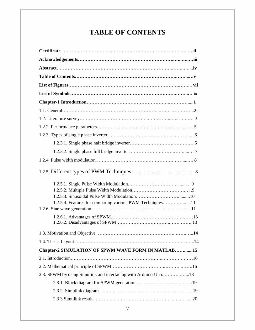
TABLE OF CONTENTS
Certificate……………………………………………………………….……..…..ii
Acknowledgements……………………………………………………..…..…..…iii
Abstract………………………………………………………………..……..…....iv
Table of Contents………………………………………………………..……...…v
List of Figures……………………………………………………………..……... vii
List of Symbols…………………………………………………………..……..… ix
Chapter-1 Introduction……………………………………………..………….....1
1.1. General……………………………………………………...……...…………..2
1.2. Literature survey……………………………………...…………...…..…….… 3
1.2.2. Performance parameters…………………………………………...….……. .5
1.2.3. Types of single phase inverter……………………………….……………... .6
1.2.3.1. Single phase half bridge inverter……………………….……….… 6
1.2.3.2. Single phase full bridge inverter……………….……….…….....… 7
1.2.4. Pulse width modulation…………………………….…………….……....…. 8
1.2.5. Different types of PWM Techniques…..……………..……......... .8
1.2.5.1. Single Pulse Width Modulation…………………………........… .9 1.2.5.2. Multiple Pulse Width Modulation…………………………….… .9 1.2.5.3. Sinusoidal Pulse Width Modulation………………………..........10 1.2.5.4. Features for comparing various PWM Techniques……….….......11 1.2.6. Sine wave generation…………………………………………….........…....11
1.2.6.1. Advantages of SPWM………………………………………..……13 1.2.6.2. Disadvantages of SPWM……………………………..…….……..13 1.3. Motivation and Objective …………………………………………..…….…..14
1.4. Thesis Layout …………………………………………………….….…....…..14
Chapter-2 SIMULATION OF SPWM WAVE FORM IN MATLAB…….......15
2.1. Introduction…………………………………………………...………….……16
2.2. Mathematical principle of SPWM……………………………..……… .…….16
2.3. SPWM by using Simulink and interfacing with Arduino Uno..………..…...18
2.3.1. Block diagram for SPWM generation………………….….… …....19
2.3.2. Simulink diagram………………………………………….…...……19
2.3.3 Simulink result……………………………………………… ……...20
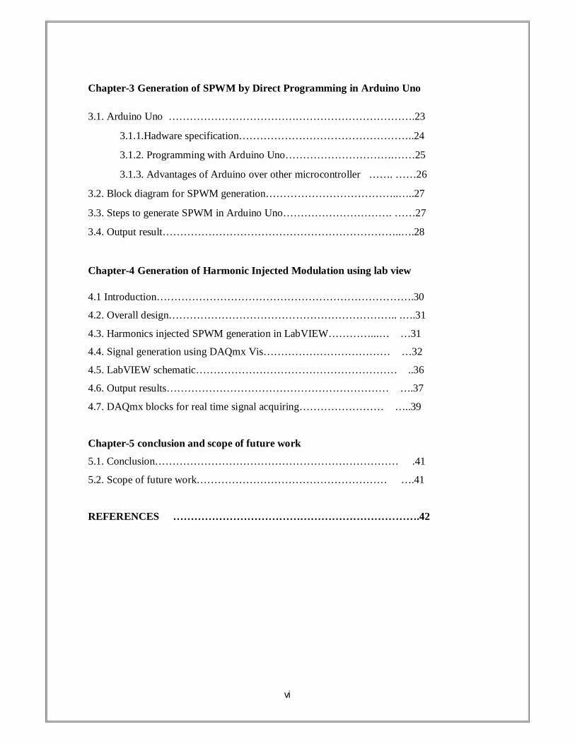
vi
Chapter-3 Generation of SPWM by Direct Programming in Arduino Uno 3.1. Arduino Uno …………………………………………………………….23
3.1.1.Hadware specification…………………………………………..24
3.1.2. Programming with Arduino Uno………………………….……25
3.1.3. Advantages of Arduino over other microcontroller ……. ……26
3.2. Block diagram for SPWM generation………………………………..…..27
3.3. Steps to generate SPWM in Arduino Uno…………………………. ……27
3.4. Output result…………………………………………………………..….28
Chapter-4 Generation of Harmonic Injected Modulation using lab view 4.1 Introduction……………………………………………………………….30
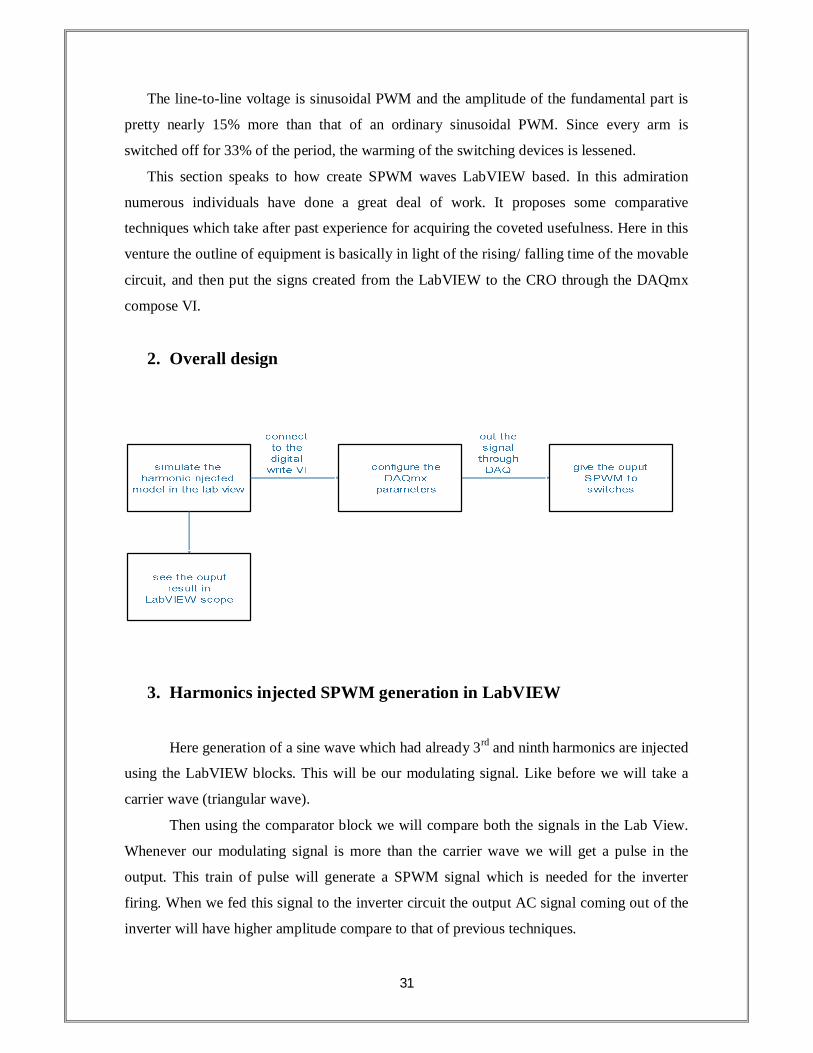
4.2. Overall design……………………………………………………….. .….31
4.3. Harmonics injected SPWM generation in LabVIEW…………...… …31
4.4. Signal generation using DAQmx Vis……………………………… …32
4.5. LabVIEW schematic………………………………………………… ..36
4.6. Output results……………………………………………………… ….37
4.7. DAQmx blocks for real time signal acquiring…………………… …..39
Chapter-5 conclusion and scope of future work
5.1. Conclusion…………………………………………………………… .41
5.2. Scope of future work……………………………………………… ….41
REFERENCES …………………………………………………………….42

vii
List of Figures
Fig. 1.1 Block diagram of a single phase inverter
Fig. 1.2.Schematic diagram of a single phase half bridge inverter
Fig. 1.3 Circuit diagram of single phase half Bridge inverter
Fig. 1.4 Circuit diagram of single phase full Bridge inverter
Fig. 1.5 Single pulse width modulation
Fig. 1.6 Multiple pulse width modulation
Fig. 1.7sinusoidal pulse modulation
Fig. 1.8(a) SPWM comparison signals
Fig. 1.8(b) Unfiltered SPWM output
Fig.1.8(c) Filtered SPWM output
Fig. 1.9 Over modulation
Fig. 2.1 Principle of the SPWM asymmetry regular sampling
Fig. 2.2(a) Simulink blocks to gennerate the array of a SPWM in workspace
Fig. 2.2(b) Simulink block diagram to take out SPWM through Arduino block
Fig. 2.3(a) Modulating wave generated in Simulink
Fig. 2.3(b) carrier wave generated in Simulink
Fig.2.3 SPWM seen in the scope of Matlab
Fig. 2.4 SPWM generated in the output pin of the Arduino Uno
Fig. 3.1 Schematic view of a Arduino Uno
Fig. 3.2(a) Block showing the programming window of Arduino Uno
Fig. 3.2(b) Blocks for the operation of the Arduino
Fig. 3.3 SPWM wave in Arduino output pin

viii
Fig4.1 Selected harmonic injection modulation Fig.4.2 Harmonics injection modulation in 3-phase
Fig.4.3 Block for selecting the DAQmx VIs
Fig. 4.4 Block for configuring the DAQmx
Fig. 4.5 Physical channel selecting block
Fig. 4.6 Start VI block
Fig. 4.7 write VI block
Fig. 4.8(a) Schematic representation for simple SPWM
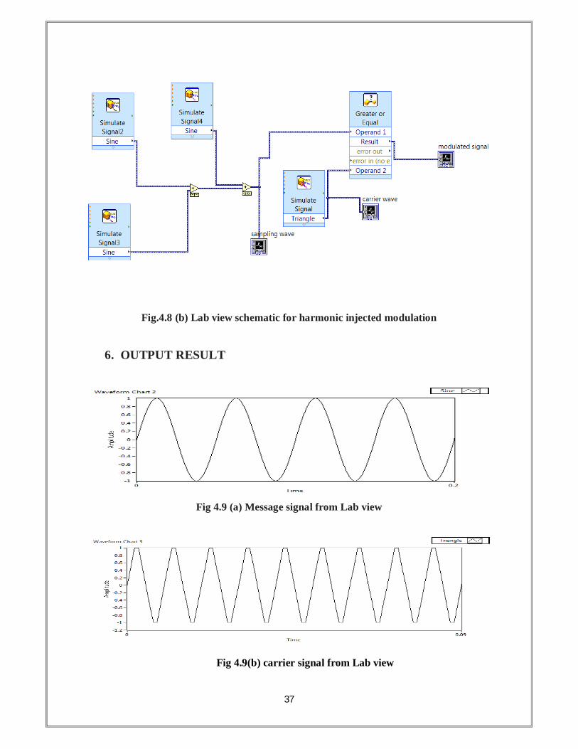
Fig. 4.8(b) Schematic representation for harmonic injected modulation
Fig. 4.9(a) Message signal from Lab view
Fig. 4.9(b) carrier signal from Lab view
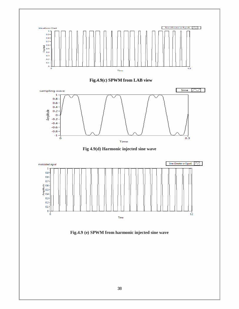
Fig. 4.9(c) ) SPWM from LAB view
Fig. 4.9(d) Harmonic injected sine wave
Fig. 4.9(e) SPWM from harmonic injected sine wave
Fig. 4.10 Blocks of DAQmx VIs for the real time generation of SPWM

ix
List of abbreviations
SPWM Sinusoidal pulse width modulation
DC Direct current
AC Alternating current
FPGA Field programmable gate array
MOSFET Metallic oxide semiconductor field effect transistor
IGBT Insulated Gate Bipolar Junction Transistor
ASD Adjustable speed drives
VSI Voltage source inverter
CSI Current source inverter
MI Modulation index
List of tables
Table-1 Switching state of half bridge inverter
Table-2 Switching state of full bridge inverter

1
Chapter 1
2
1.1 Introduction
The dc/ac inverters are the important power electronic conversion devices in
renewable energy production, motor drives, and mainly uninterruptible power supply
applications. An improved single-stage, full scaffold dc/ac power converter (inverter) is given
beneath. The sinusoidal pulse width modulation (SPWM) procedure is generally utilized as a
part of request to modify the dc/ac inverter yield voltage sufficiency and frequency as
indicated by the sought qualities. This case power rectifier switching devices (e.g. MOSFETs,
IGBTs, and so on.) are situated to ON or OFF states as per the consequence of the
examination between a very high recurrence, practically consistent adequacy triangular wave
(likewise called carrier) with a low-frequency (50Hz) reference of customizable amplitude or
frequency. A simplified single-phase, full bridge dc/ac power converter (inverter) is given
below. The sinusoidal pulse width modulation (SPWM) technique is conventionally preferred
as it is to adjust the dc/ac inverter output voltage amplitude and frequency according to the
desired values. This case power rectifier switches (e.g. MOSFETs, IGBTs, etc.) are fixed to
TURN ON or OFF states depending on the outcome of the comparison of a very high
frequency, almost constant-amplitude triangular wave (also called carrier) which have a low-
frequency (50Hz) reference of adjustable frequency or amplitude.
The DC-AC inverters are generally fired with Pulse Width Modulation (PWM)
technique. This PWM which is a quite useful and advanced procedure in which Gate pulse’s
width is controlled by employing different techniques. The PWM inverter does not depend
upon the output load instead it changes the inverter voltage at rated load. Conventionally in
an inverter circuit, the output voltage varies according to the load attached with the inverter
circuit. To reduce the effect of load-changing, the PWM inverter regulates the output voltage
by varying the width of the gate pulses (duty cycle) and thus the output of the inverter. The
AC output voltage which is regulated by the change in the frequency of the output pulse and
change pulse width which are varied depending up on the type of load connected in the
output of the system in order to make available fixed output. The inverters generally engage
in a sinusoidal pulse width modulated (SPWM) policy and changes between two different
circuit connections, from which it is clear that inverter is a nonlinear device, preferably
piecewise steady system. Furthermore, the control strategies which are employed in the
inverters are almost similar to that used in in DC-DC converters.

3
1.3. Literature survey
The output voltage waveform of a perfect inverter must be sinusoidal hypothetically,
however the waveform of pragmatic inverters are by and large not sinusoidal and contains
different harmonics. Square-wave or semi square-wave voltages are utilized for most of the
low and medium power applications. For high-control applications and less distorted
sinusoidal wave, bridge structures are generally preferred. At present by and large high speed
power semiconductors are accessible, so the harmonics in the yield voltage can be minimized
or decreased altogether by distinctive exchanging methods.
Here in the following there is a circuit diagram of a full bridge inverter is given.
Fig.1.1. Block diagram of a single phase inverter
Inverters are divided in two groups: (1) single-stage inverters, and (2) three-stage
inverters. Either of these employ controlled turn-on and turn-off devices (e.g. metal oxide
semiconductor field-effect transistors [MOSFETs], bipolar junction transistors (BJT),
insulated-gate bipolar transistors [IGBT], and metal oxide semiconductor controlled
thyristors [GTO’s]. These inverters employ pwm control signals for generating sinusoidal
output alternating voltages.

4
Depending upon the input sources also the inverters are also of two types.
Voltage Source Inverter
At the point when the dc yield voltage of an inverter stays steady it is called VSI. The
load does not influence the yield voltage of the inverter. Due to this property, the VSI is by
and large utilized as a part of industrial applications like Adjustable speed drives (ASD) and
generally in Power systems for FACTS (Flexible AC Transmission).
Current Source Inverter
At the point when the dc yield current of an inverter stays steady it is called CSI. The
load does not influence the yield current of the inverter. We use these inverters where high
quality waveforms are required, for example in medium voltage industrial applications.
1.2.1 Principle of operation of single phase inverter
The principle of single phase operation can be explained with the following circuit
diagram. The inverter made up of two choppers back to back. When only transistor Q1 is
turned on for a time 푇 /2, the instantaneous voltage crosswise the load 푣 appears as 푣 2 . If
only transistor Q2 is only turned on for a time푇 /2, voltage appearing across the load is -푣 2
. So the circuit has to be designed in such a way that the transistors, Q1 and Q2 are not turned
on simultaneously.
The root means square output voltage can be calculated as :-
푣 = ∫ dt =푣 2
The Fourier series analysis of instantaneous output voltage is:
푣 = + ∑ (푎 cos(푛휔푡) + 푏 sin(푛휔푡))

5
Fig.2. single phase half bridge inverter
1.2.2. Performance parameters
Normally harmonics are present in the inverter output and the inverter quality can be
expressed as follows.
1. Harmonic factor of nth harmonic (푯푭풏)
The contribution of individual harmonic component is known as the harmonic
factor (of the nth harmonic). Given by
퐻퐹 = for n > 1
Where 푉 means the fundamental component expressed in rms terms.
푉 is nth harmonic component expressed in rms terms.
2. Total harmonic distortion (THD)
The total harmonic distortion is a means of how closely the fundamental
component follows the shape of the resultant waveform. It is given by
THD = (∑ 푉 ), , …

6
3. Distortion factor(DF)
THD implies the sum of total harmonic content, but generally not focus how
much total harmonics it contains. The filter employed at the inverter output shows that
the higher order harmonics can be obtained more efficiently. So it is important to
know about both the frequency and amplitude of harmonics. For a second order load
filter DF is defined as
DF= [∑ ( ) ), ,…. ]
4. Lowest order harmonic
The frequency of the harmonic component which is closest to the fundamental
component is known as LOH, and thus amplitude is greater or equal to 3% of the
fundamental in the wave.
1.2.3. Types of single phase inverter
1.2.3.1. Single Phase Half Bridge Inverter
Half bridge inverter consists of power electronics switches T2 and T1. The switch
used here can be a BJT, an IGBT or simply a Thyristor. Freewheeling diode D2 and D1 are
called also known as the Feedback diodes are also connected to feedback the reactive power
of the load.
Fig 1.3: Single Phase Half Bridge Inverter

7
T1 T2 푣
ON OFF +
ON OFF −
Table 1: Switching States
Amid the positive half cycle of the yield voltage T1 switch is ON, which empowers
the yield voltage Vout = Vo/2 and amid the negative half cycle T2 is ON which makes Vout=
-Vo/2. The switches work on the other hand not at the same time to stay away from the
possibilities of short-circuiting. At the point when resistive load is in the output, the present
waveform is same as that of voltage wave shape however when reactive load is associated
both are diverse. For a reactive load, the freewheeling diodes act only there is opposite
polarities between the current and voltages.
1.2.3.2. Single Phase Full Bridge Inverter
This comprises of 2 diverse power electronics switches on the arms of inverter and
four freewheeling diodes which help in releasing the reverse current. At the point when
resistive-inductive load is joined through the diode opposite load current flows. Diodes
ordinarily give the substitute way to the inductive current which likewise flows amid the turn
off period.
Fig 1.4 Single Phase Full wave Bridge Inverter
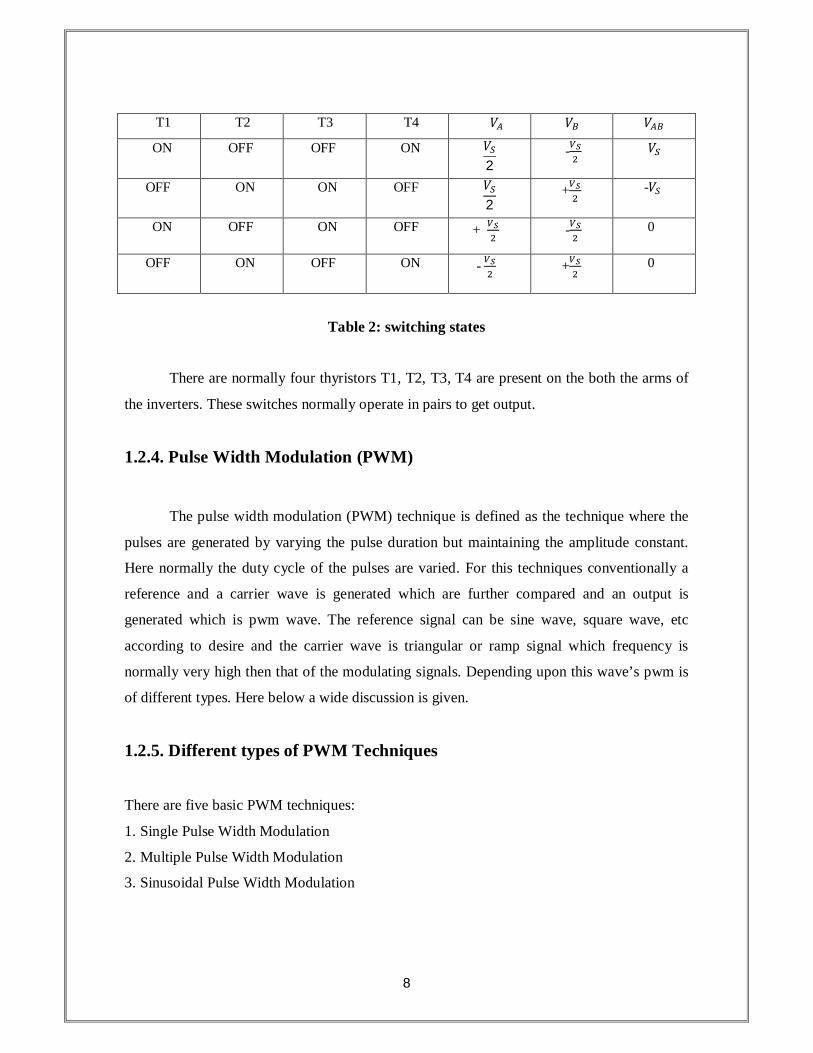
8
T1 T2 T3 T4 푉 푉 푉
ON OFF OFF ON 푉2
- 푉
OFF ON ON OFF 푉2
+ -푉
ON OFF ON OFF + - 0
OFF ON OFF ON - + 0
Table 2: switching states
There are normally four thyristors T1, T2, T3, T4 are present on the both the arms of
the inverters. These switches normally operate in pairs to get output.
1.2.4. Pulse Width Modulation (PWM)
The pulse width modulation (PWM) technique is defined as the technique where the
pulses are generated by varying the pulse duration but maintaining the amplitude constant.
Here normally the duty cycle of the pulses are varied. For this techniques conventionally a
reference and a carrier wave is generated which are further compared and an output is
generated which is pwm wave. The reference signal can be sine wave, square wave, etc
according to desire and the carrier wave is triangular or ramp signal which frequency is
normally very high then that of the modulating signals. Depending upon this wave’s pwm is
of different types. Here below a wide discussion is given.
1.2.5. Different types of PWM Techniques
There are five basic PWM techniques:
1. Single Pulse Width Modulation
2. Multiple Pulse Width Modulation
3. Sinusoidal Pulse Width Modulation
9
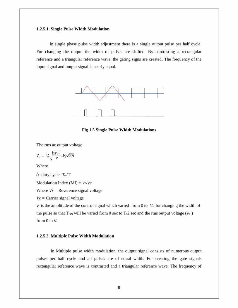
1.2.5.1. Single Pulse Width Modulation
In single phase pulse width adjustment there is a single output pulse per half cycle.
For changing the output the width of pulses are shifted. By contrasting a rectangular
reference and a triangular reference wave, the gating signs are created. The frequency of the
input signal and output signal is nearly equal.
Fig 1.5 Single Pulse Width Modulations
The rms ac output voltage
푉 = 푉 =푉√2훿
Where
=duty cycle=Ton/T
Modulation Index (MI) = Vr/Vc
Where Vr = Reverence signal voltage
Vc = Carrier signal voltage
Vr is the amplitude of the control signal which varied from 0 to Vc for changing the width of
the pulse so that TON will be varied from 0 sec to T/2 sec and the rms output voltage (Vo )
from 0 to Vs.
1.2.5.2. Multiple Pulse Width Modulation
In Multiple pulse width modulation, the output signal consists of numerous output
pulses per half cycle and all pulses are of equal width. For creating the gate signals
rectangular reference wave is contrasted and a triangular reference wave. The frequency of

10
the reference signals determines the output frequency (fo) and transporter frequency (fc ).
The number of pulses per half cycle is determined by p: p= fc /2fo.
Fig 1.6 multiple pulse width modulation
The rms ac output voltage
푉 = 푉푝훿휋
=duty cycle=Ton/T
The modulation index (MI) varies from 0 to 1 for the pulse from 0 to p/p and the output
voltage varies from 0 to Vs.
1.2.5.3. Sinusoidal Pulse Width Modulation
In sinusoidal pulse width modulation procedure there are different quantities of output
pulses per half cycle and the pulses have varying width. The width of every pulse is differing
in extent to the amplitude of a sine wave assessed at the focal point of the same pulse. For
producing the gating signals a sinusoidal reference wave is contrasted and a high frequency
triangular signal. The rms ac output voltage.
푉 = 푉푝훿휋
Where p=number of pulses and d= pulse width
11
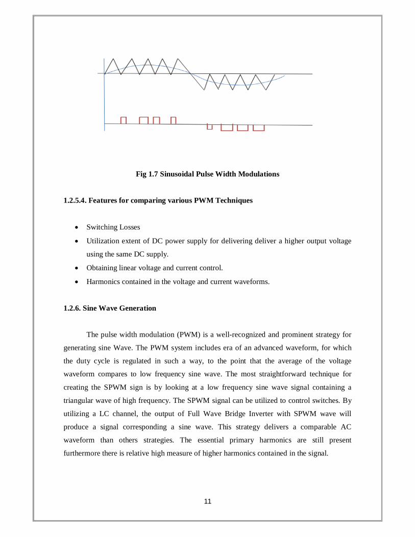
Fig 1.7 Sinusoidal Pulse Width Modulations
1.2.5.4. Features for comparing various PWM Techniques
Switching Losses
Utilization extent of DC power supply for delivering deliver a higher output voltage
using the same DC supply.
Obtaining linear voltage and current control.
Harmonics contained in the voltage and current waveforms.
1.2.6. Sine Wave Generation
The pulse width modulation (PWM) is a well-recognized and prominent strategy for
generating sine Wave. The PWM system includes era of an advanced waveform, for which
the duty cycle is regulated in such a way, to the point that the average of the voltage
waveform compares to low frequency sine wave. The most straightforward technique for
creating the SPWM sign is by looking at a low frequency sine wave signal containing a
triangular wave of high frequency. The SPWM signal can be utilized to control switches. By
utilizing a LC channel, the output of Full Wave Bridge Inverter with SPWM wave will
produce a signal corresponding a sine wave. This strategy delivers a comparable AC
waveform than others strategies. The essential primary harmonics are still present
furthermore there is relative high measure of higher harmonics contained in the signal.
12
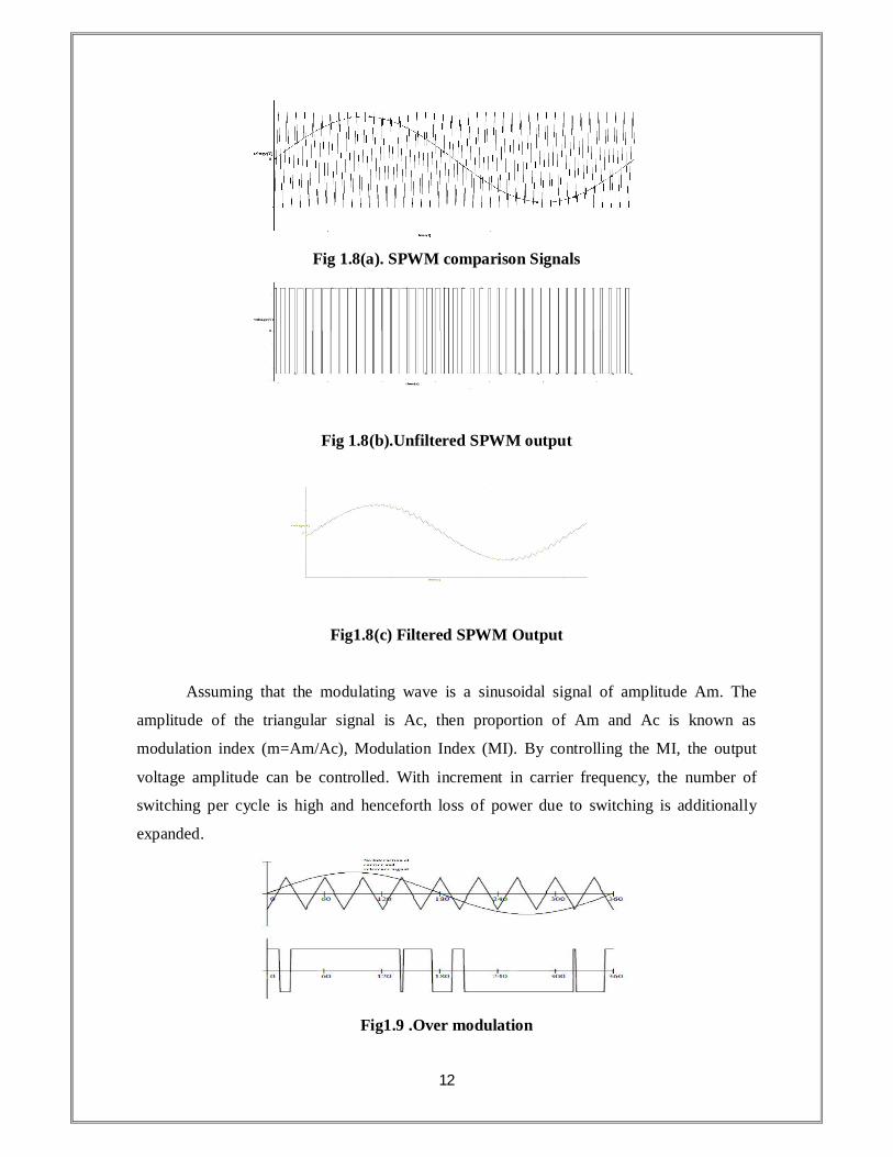
Fig 1.8(a). SPWM comparison Signals
Fig 1.8(b).Unfiltered SPWM output
Fig1.8(c) Filtered SPWM Output
Assuming that the modulating wave is a sinusoidal signal of amplitude Am. The
amplitude of the triangular signal is Ac, then proportion of Am and Ac is known as
modulation index (m=Am/Ac), Modulation Index (MI). By controlling the MI, the output
voltage amplitude can be controlled. With increment in carrier frequency, the number of
switching per cycle is high and henceforth loss of power due to switching is additionally
expanded.
Fig1.9 .Over modulation
13
For Modulation index less than 1, the inciter process works well but for MI greater
than 1, their chances that the triangle wave will not intersect with carrier wave and the result
is shown in the fig. 11. But a certain amount of “over modulation” is often allowed for
obtaining a higher AC output voltage at the cost of increased harmonic content in the output
voltage waveform.
1.2.6.1. Advantages of SPWM
Low power utilization.
High vitality effective up to 90%.
High power taking care of ability.
No temperature variety and maturing brought about floating or debasement in
linearity.
Easy to actualize and control.
Easily compatible with microprocessor’s.
1.2.6.2. Disadvantages of SPWM
Attenuation of the desired fundamental component in the waveform.
Significant increase in switching frequencies which leads to increased stress on the
connected switching devices and this leads to derating of these devices.
Generation of high-frequency harmonic components.

14
1.3. Motivation and objective of the work
The digital executions of Sinusoidal Pulse Width Modulation (SPWM) generators
have overwhelmed over their partners taking into account analog circuits. It has a flexible
architecture that can be tuned to a variety of single-phase dc/ac inverter applications. Now a
days with the improvement in the microcontroller field have brought a vast change in the
digital circuits and had made easy to generate the desired signals. Arduino Uno is a on board
microcontroller, easy to control and code and very simple to integrate with other software
like MATLAB Simulink and LAB VIEW. So we will try to generate the SPWM signal
using Arduino Uno incorporated with Matlab or directly with the microcontroller.
1.4. Thesis layout
Chapter2: Chapter 2 discuss the simulation of the sinusoidal pulse width modulation using
MATLAB Simulink. Then using Arduino package which is already installed in the Matlab,
give this SPWM signal to the Arduino through this driver.
Chapter 3: Chapter 3 discuss the direct generation of SPWM signal in the Arduino Uno using
the mathematical model through programming in Arduino base.
Chapter 4: Chapter 4 discuss the harmonic injection in the SPWM signal and its advantages
using LABVIEW. Further we will try to signal out through the DAQmx and give it to the
firing circuit of inverter.
Chapter 5: This chapter discusses the different result extracted from above 3 methods and
compare them. It also contains the conclusion and the scope of future work of this particular
research work.

15
Chapter -2
16
SIMULATION OF SPWM WAVE FORM IN MATLAB
2.1. Introduction
Designing a single phase inverter of rating 9v(ac),for different experimental lab
purposes, the basic things we have to consider are simulation of the inverter circuit;
simulation and hardware design of the firing circuit.
There are different strategies for producing SPWM waveforms. One of them is
Regular sampling method is considered as a cutting edge engineering method. In general
sampling method, the triangle wave is considered like the carrier which specimen the sine
wave. At the point when the sine wave is sampled at the vertices or at most lowest point of
the triangle wave, this technique is called symmetrical regular sampling. At the point where
sampling sites is at both points top and base point this is known as the asymmetric regular
sampling. As a consequences in the increment of sampling sites, the adjustment in the square
wave duty ratio is all the more near to sine principle. Subsequently the SPWM shaped by
asymmetric regular sampling is firmly estimated to the sine wave than the symmetric
sampling. Subsequently, the harmonic component of amplitude gets significantly littler.
Because of this reason, the asymmetric regular sampling technique is picked in this work.
The triangular wave as the carrier, at the positive or negative half cycle of sine wave, has just
single polarity and the SPWM waveform changes just inside of the extent of single polarities
in half cycle. This generation technique is known as the single polarity SPWM control mode.
In the event that the triangle wave becomes bipolar in every other half a cycle of the sine
wave, the SPWM waveform will be certain and negative amid the half, and this is the thing
that called as bipolar SPWM control mode.
2.2. Mathematical Principle of SPWM
The principle of SPWM uses sine as the modulation wave, isosceles tringle as the
carrier, when the tringle wave and sine wave curve intersect, the control signal is produced at
the intersection point to control on-off of power switch device. A series of constant amplitude
and pulse width is proportional to corresponding interval sine wave curve function values of
rectangular pulse can be got. From the mathematical point of view, SPWM wave is set of

17
pulse according to certain rule change. This rule can be separated from analog control circuit.
The output can be controlled by this in chips.
There are several sampling methods, the natural sampling method symmetrical
sampling method, asymmetrical sampling methods. Here we will use symmetrical sampling
method to produce our SPWM signal. Triangular carrier peak is the sampling point, make a
vertical line and intersect the modulation wave at point B. a horizontal is made line at point B
and intersects the triangular carrier at point C and D. point C and D respectively is open and
shut off moment of switch devices. Rule sampling method is shown in the figure.
Fig.12. Principle of the SPWM asymmetry regular sampling
In this, the average symmetry sampling schematic is utilized for configuration. In this
strategy, the triangular waves and sine waves are contrasted and one another and test in each
sample triangular wave’s trough. A high pulse width which is express by AB width (Ton) can
be figured by trigonometric function.
As per the standard of the generation as displayed in diagram over, the mathematical
model has been created as takes after. Tc is taken as the carrier period; f is taken as frequency
of modulating wave; M as modulation coefficient which is equivalent to the proportion of the
peak estimation of the sine wave to that of the tringle wave. The available time respectively
sampled at vertex and bottom point through the graph are :
푡 푇2 × [1 + 푀 × sin(휔푡 )]
푡 =푇2 × [1 + 푀 × sin(휔푡 )]
18
Carrier wave ratio: 푁 = = ∗
Vertex and bottom time respectively are:
푡 =푇2 × 푘(푘 = 0,2,4,2푁 − 2)
푡 = 푇2 × 푘(푘 = 1,3,5, … ,2푁 − 1))
푡 =푇2 × 1 + 푀 × sin
푘 휋1푁
(푘 = 0,2,4, … . ,2푁 − 2)
푡표푛2 = 푇2 × [1 + 푀 × sin(
푘 휋1푁 )](푘 = 0,2,4, … .2푁 − 2)
The PWM effective pulse duration is obtained as:
푡 = 푡 + 푡
The duty ratio of each cycle is calculated from the formula.t= sampling time. wt- =k*
is the carrier wave ratio. The duty cycle of each triangular carrier can be calculated only need
to look up table which include the value of the sine function at the sampling time.
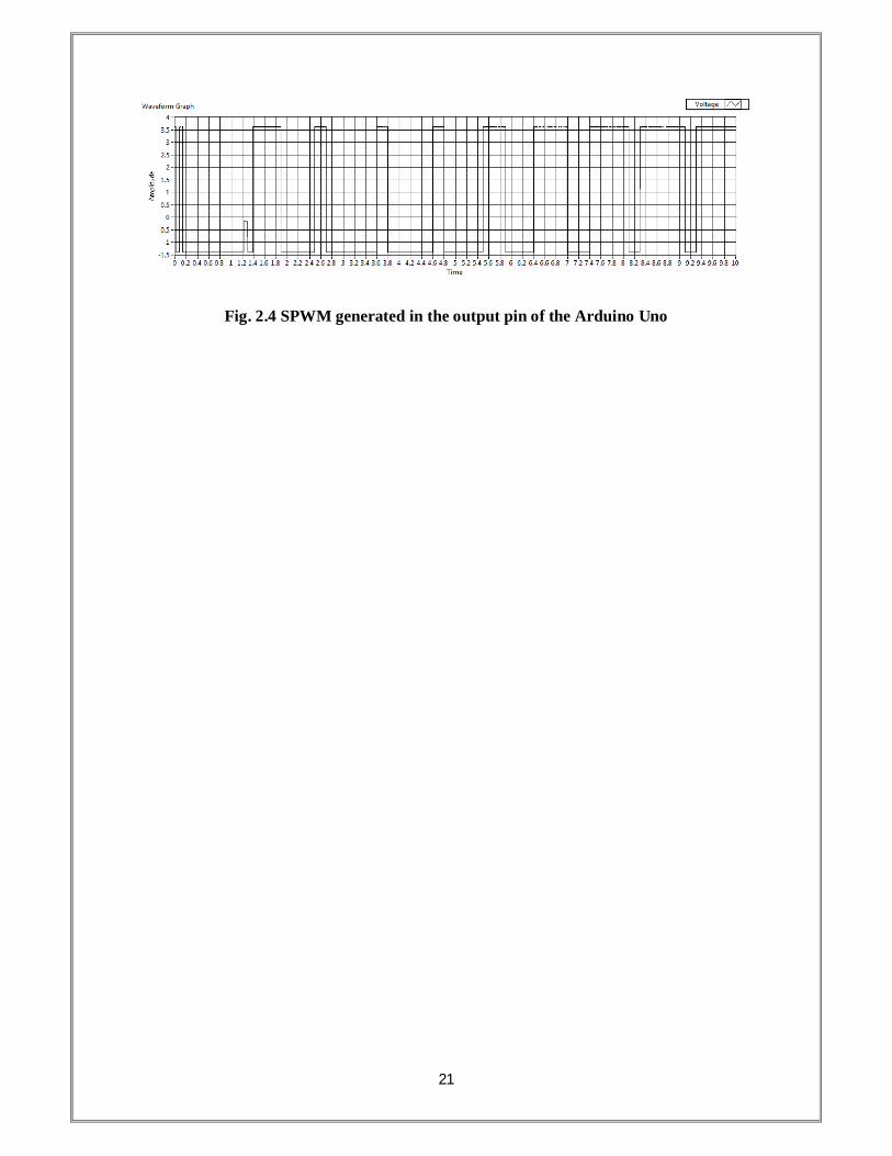
2.3. SPWM By using Simulink and interfacing with Arduino Uno
In this method first we simulate the SPWM wave by comparing sine wave (sampling
wave) of frequency 5hz and the triangular wave (carrier wave) of frequency 100 Hz. For this
we use the ODE 23 solver. After getting the SPWM signal we feed it to the workspace to get
the sampled values of SPWM signal in a array. As we aware that hardware interface the will
run with only fixed steps (i.e. ODE 3 solver) so we cannot give the generated spwm signal
into the Arduino block.
After getting the sampled values from this simulation block we will use different
window for hardware interface. In this window using “Lookup Table” block we retrieve the
values of SPWM signal as generated previously. For the hardware interface we connect the
Arduino Uno and set the pin no and other parameters Then we will be able to get the desired
output pin of Arduino Uno. For real time analysis of the wave from coming from the Arduino
Uno pin we use the Lab View connected to The DAC. In this method the major drawback is
that here the sampling frequency of the SPWM is limited to only 100 Hz. For generating the
higher sampling frequency it will take a very large amount of the sampled wave in look up

19
table. Which will be very big enough for the Flash memory of the Arduino Uno
microcontroller (Atmega 328) which is 8 bit? Another Problem in this method is that
simulation run rime is very low (max=100 s). But in real time application for long time
application of inverter we have to reset the hardware again and again. So we will follow the
next method.
2.3.1. Block diagram to generate SPWM in MATLAB Simulink:
2.3.2. Simulink Diagram:
Fig.2.2(a) Simulink blocks to gennerate the array of a SPWM in workspace
Fig.2.2 (b) Simulink block diagram to take out SPWM through Arduino block

20
3.3. Simulink result
Fig.2.3(a) modulating sine wave generated in simulink
Fig.2.3(a) carrier wave generated in simulink
Fig.2.3(c) SPWM seen in the scope of Matlab
21
Fig. 2.4 SPWM generated in the output pin of the Arduino Uno

22
Chapter -3

23
Generation of SPWM by Direct Programming in Arduino
Uno
1. Arduino Uno
Arduino Uno is likewise a propelled kind of microcontroller which utilizes
ATmega328. It comprise 14 advanced data/yield pins (out of 6 pins utilized for PWM
applications),6 for analog signals, crystal oscillator of 16 MHz, an ICSP header, a USB
association, a power jack, and a reset switch. It additionally have everything as in a
microcontroller; so we have to recently interface it to a PC through a USB link else power it
with an AC-to-DC connector or battery for beginning. The Arduino Uno is not quite the same
as all past microcontroller sheets in that it doesn't utilize the FTDI USB-to-serial driver chip.
Other than it utilizes the Atmega8U2 which is customized as a USB-to-serial converter.
"Uno" is initially Italian and is named to demonstrate the forthcoming Arduino 1.0. The
version1.0 and Uno will be the reference variants of Arduino, in the movement. The Uno is
the rendition of USB Arduino sheets, and is utilized as the reference for the forthcoming
boards.
Fig.3.1 Schematic view of a Arduino Uno
24
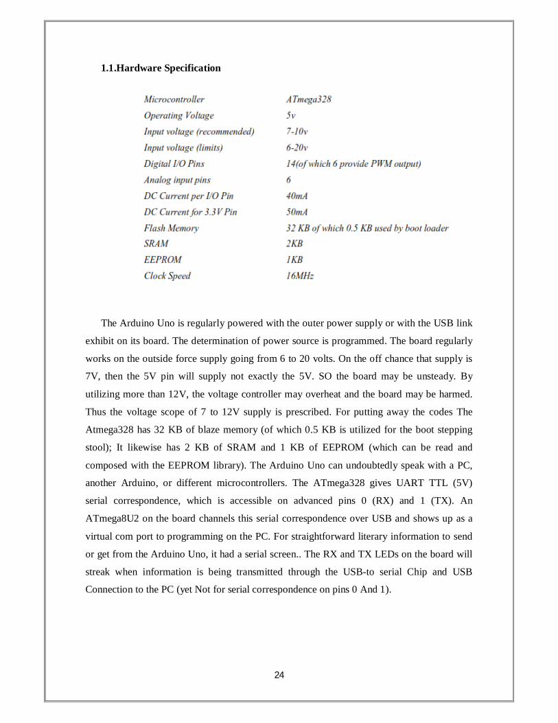
1.1.Hardware Specification
The Arduino Uno is regularly powered with the outer power supply or with the USB link
exhibit on its board. The determination of power source is programmed. The board regularly
works on the outside force supply going from 6 to 20 volts. On the off chance that supply is
7V, then the 5V pin will supply not exactly the 5V. SO the board may be unsteady. By
utilizing more than 12V, the voltage controller may overheat and the board may be harmed.
Thus the voltage scope of 7 to 12V supply is prescribed. For putting away the codes The
Atmega328 has 32 KB of blaze memory (of which 0.5 KB is utilized for the boot stepping
stool); It likewise has 2 KB of SRAM and 1 KB of EEPROM (which can be read and
composed with the EEPROM library). The Arduino Uno can undoubtedly speak with a PC,
another Arduino, or different microcontrollers. The ATmega328 gives UART TTL (5V)
serial correspondence, which is accessible on advanced pins 0 (RX) and 1 (TX). An
ATmega8U2 on the board channels this serial correspondence over USB and shows up as a
virtual com port to programming on the PC. For straightforward literary information to send
or get from the Arduino Uno, it had a serial screen.. The RX and TX LEDs on the board will
streak when information is being transmitted through the USB-to serial Chip and USB
Connection to the PC (yet Not for serial correspondence on pins 0 And 1).

25
1.2.Programming with Arduino Uno
Principally Arduino programming is utilized for the programming of the Arduino Uno
(effortlessly accessible in the web). From the Tools > Board menu (as indicated by the
microcontroller on your board) select the "Arduino Uno w/ATmega328". The ATmega328 on
the Arduino Uno accompanies a pre burned boot loader which permits you for transferring
new codes in it without utilizing the outer equipment software engineer. It additionally
utilizes the first STK500 convention (reference C header records) for interchanges. You can
likewise straightforwardly program the microcontroller through the ICSP (In-Circuit Serial
Programming) header bypassing the boot loader. The ATmega8U2 firmware source code is
accessible. The ATmega328 is stacked with a DFU boot loader, which is by and large
actuated by interfacing the bind jumper on the back of the board and after that resetting the
8U2. You can likewise then utilize Atmel's FLIP programming (Windows) of the DFU
developers (MacOS X and linux) for stacking the new firmware. Else you can utilize the ISP
header with the outside software engineer (which over warmth the DFU boot loader)
Before transferring, the Arduino Uno has composed in such a path, to the point that it
permits to resetting by programming running on a joined PC, rather physical squeezing of the
rest catch. It is conceivable as one of the equipment stream control lines (DTR) Of the
ATmega8U2 is associated with the ret lines of the ATmega328 by means of a 100 Nano farad
capacitors.
Arduino as a microcontroller had the capacity to sense the encompassing by getting
information inputs utilizing distinctive sensors furthermore can influence nature by utilizing
lights, engines, and different actuators. The Arduino programming dialect (in view of wiring)
is utilized to program the microcontroller. Arduino is intended for tasks which can be either
remain solitary or they can speak with programming which keeps running on a PC (e.g.
Glimmer, Processing, MaxMSP). Arduino is a cross-stage program. On need to take after
different direction as per the individual OS. First and foremost we will attempt to "smolder"
our first program on the Arduino Uno, a no doubt understood and generally utilized
programming "hi world".
For this select
File>Sketchbook>Arduino-0017>Examples>Digital>Blink
Once we open this folder there will be a folder looking like something given below.
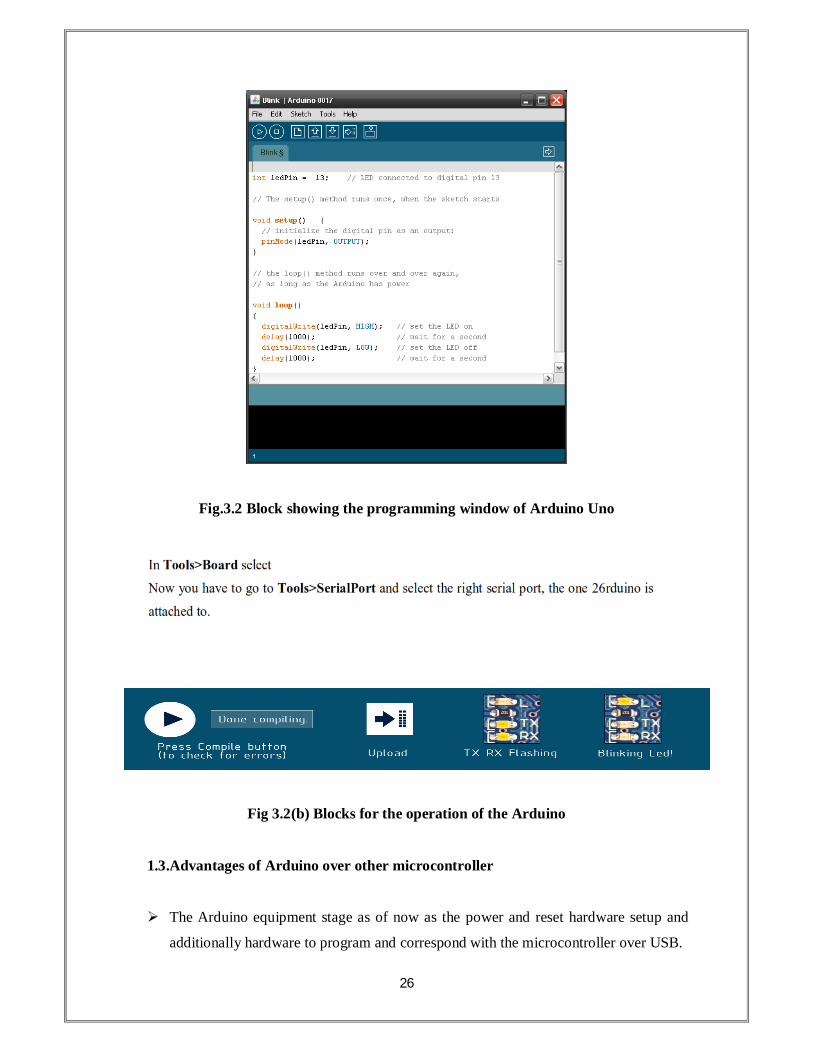
26
Fig.3.2 Block showing the programming window of Arduino Uno
Fig 3.2(b) Blocks for the operation of the Arduino
1.3.Advantages of Arduino over other microcontroller
The Arduino equipment stage as of now as the power and reset hardware setup and
additionally hardware to program and correspond with the microcontroller over USB.
27
I/O pins of the microcontroller are normally as of now encouraged out to
attachments/headers for simple access.
On the product side, Arduino gives various libraries to make programming thee
microcontroller simpler. The most straightforward of these are capacities to control
and read I/O sticks as opposed to having fiddled with the bus/bit makes regularly used
to interface with Atmega I/O.
Here according to my need there are specifically designed pins for pwm generation.
And with this platform easy to generate a SPWM wave and use in real-time unlike the
other micro controller where this need additional power supply, additional burner and
a complicated programming.
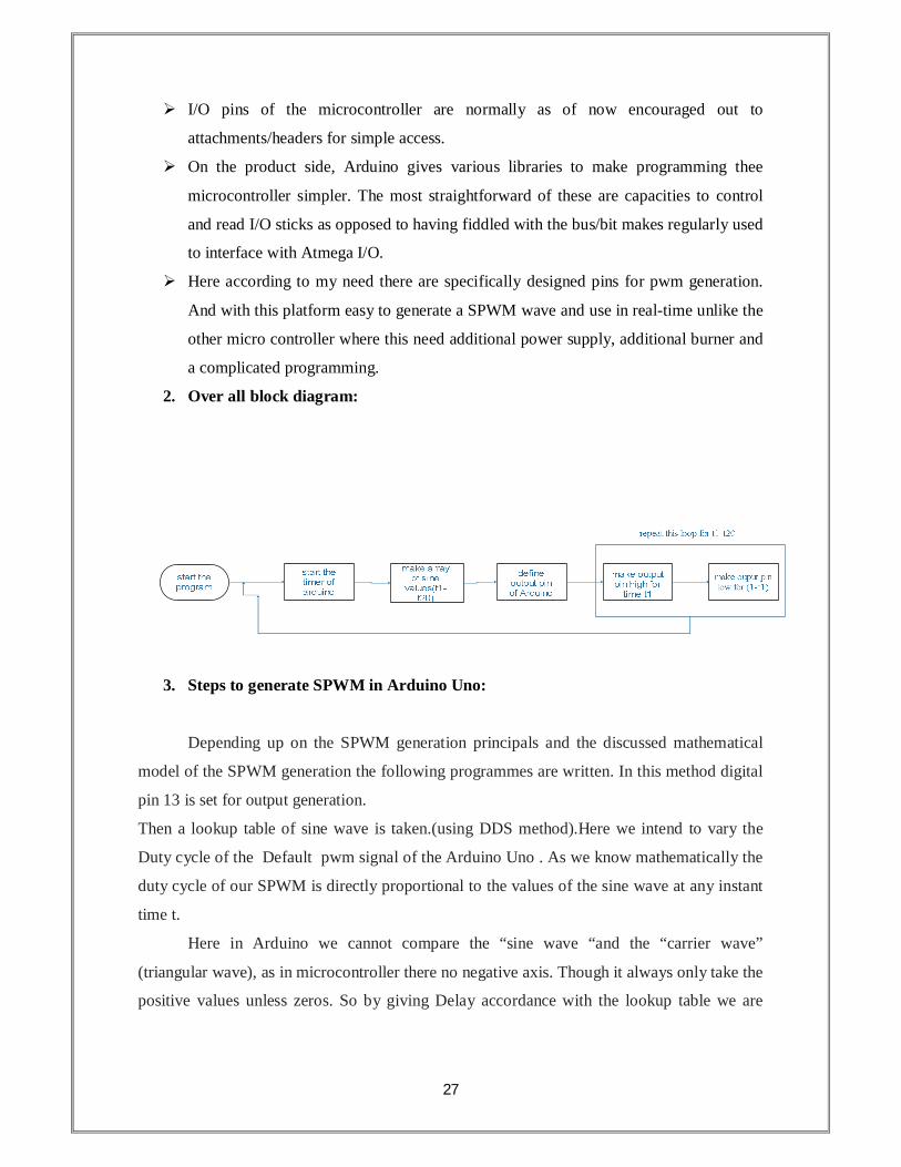
2. Over all block diagram:
3. Steps to generate SPWM in Arduino Uno:
Depending up on the SPWM generation principals and the discussed mathematical
model of the SPWM generation the following programmes are written. In this method digital
pin 13 is set for output generation.
Then a lookup table of sine wave is taken.(using DDS method).Here we intend to vary the
Duty cycle of the Default pwm signal of the Arduino Uno . As we know mathematically the
duty cycle of our SPWM is directly proportional to the values of the sine wave at any instant
time t.
Here in Arduino we cannot compare the “sine wave “and the “carrier wave”
(triangular wave), as in microcontroller there no negative axis. Though it always only take the
positive values unless zeros. So by giving Delay accordance with the lookup table we are
28
varying the duty cycle. In this method also we can vary the sampling frequency of the SPWM
as much as we want cause we can measure and generate waves in terms of MHZ.
And also this is a on board programing this can work for long enough time for the real time
application.
In our daily use and home appliances uses 50 Hz supplies and most of the industrial
application is also uses 50 Hz so we will use a carrier frequency of 20 KHz and a sampling
wave of 50 KHz.
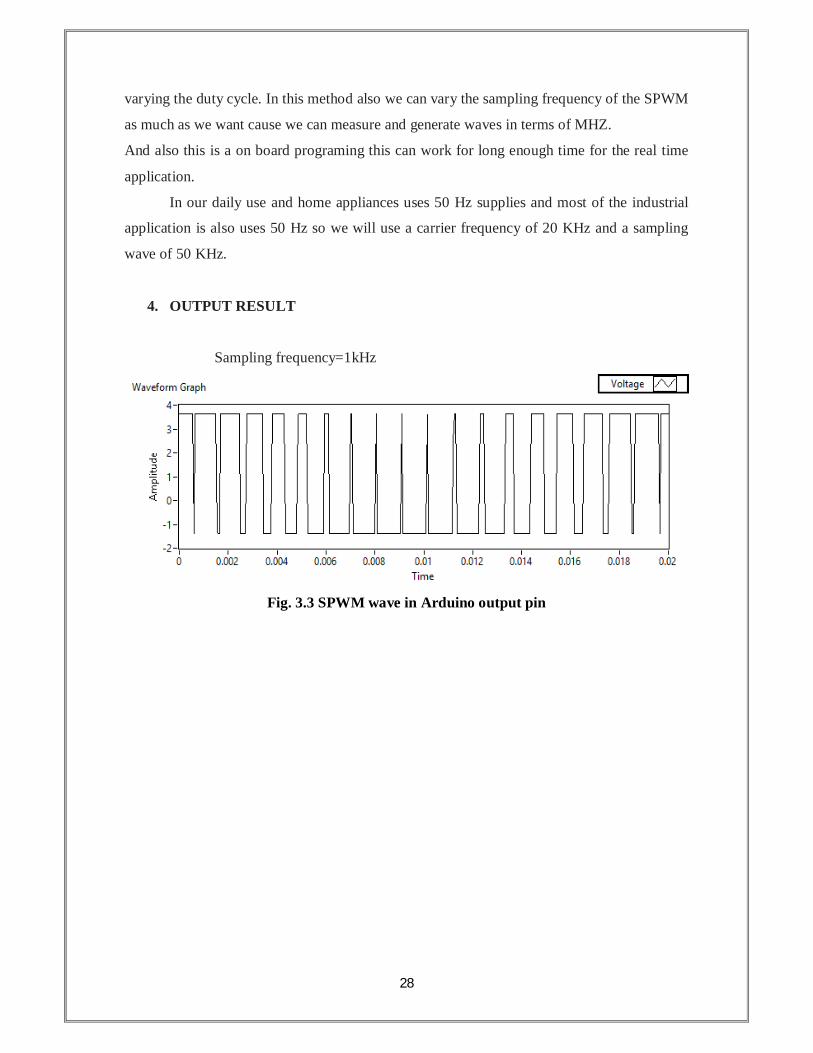
4. OUTPUT RESULT
Sampling frequency=1kHz
Fig. 3.3 SPWM wave in Arduino output pin

29
Chapter -4
30
Generation of Harmonic Injected Modulation using
LabVIEW
1. Introduction
The usually utilized SPWM, experiences different downsides like low fundamental
output voltage and so forth. Alternate procedures that take out the disadvantage of SPWM
are:
Trapezoidal modulation
Staircase modulation
Stepped modulation
Harmonic injection modulation
Delta modulation
By analysis the harmonic injected modulation is found to be the best technique for
improving the magnitude of the output voltage which is given below.
The modulating signal is produced by infusing chose harmonics with the sine wave
which brings about flat topped waveform and lessens the measure of over modulation. It
gives a low distortion and fundamental amplitude of output voltage.
We can represent a signal with harmonics like
Vr = 1.15 sin ωt + 0.27 sin 3ωt – 0.029 sin 9ωt
Modulating signal with third and ninth harmonic is injected. The injection of 3nth harmonics
does not affect the quality of the output voltage, because the output of a three phase inverter
doesn’t contain triplen harmonics.
If only the third harmonic is injected, Vr is given by
Vr = 1.15 sin휔푡+ 0.19 sin 3휔푡
31
The line-to-line voltage is sinusoidal PWM and the amplitude of the fundamental part is
pretty nearly 15% more than that of an ordinary sinusoidal PWM. Since every arm is
switched off for 33% of the period, the warming of the switching devices is lessened.
This section speaks to how create SPWM waves LabVIEW based. In this admiration
numerous individuals have done a great deal of work. It proposes some comparative
techniques which take after past experience for acquiring the coveted usefulness. Here in this
venture the outline of equipment is basically in light of the rising/ falling time of the movable
circuit, and then put the signs created from the LabVIEW to the CRO through the DAQmx
compose VI.
2. Overall design
3. Harmonics injected SPWM generation in LabVIEW
Here generation of a sine wave which had already 3rd and ninth harmonics are injected
using the LabVIEW blocks. This will be our modulating signal. Like before we will take a
carrier wave (triangular wave).
Then using the comparator block we will compare both the signals in the Lab View.
Whenever our modulating signal is more than the carrier wave we will get a pulse in the
output. This train of pulse will generate a SPWM signal which is needed for the inverter
firing. When we fed this signal to the inverter circuit the output AC signal coming out of the
inverter will have higher amplitude compare to that of previous techniques.

32
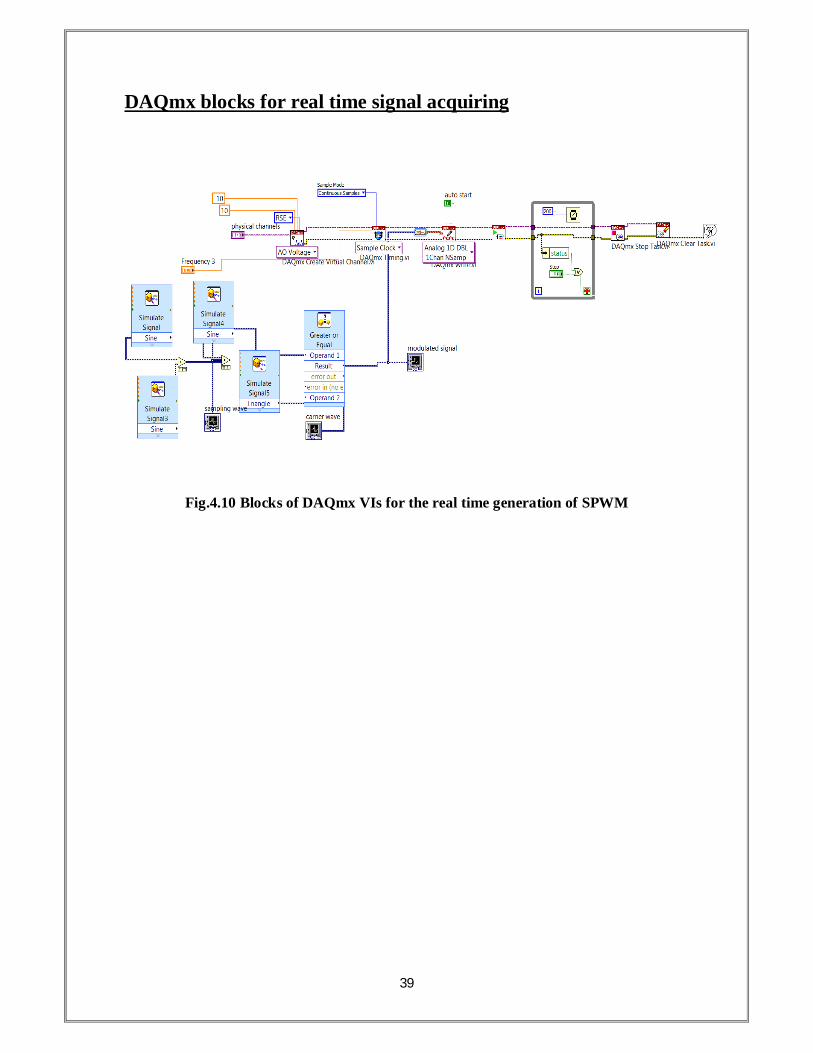
But after generating the SPWM in the Lab View we need to get the signal out using DAQ.
But as for this continues sampling we simply cannot connect the DAQ through the DAQ
block which is preinstalled in the Lab View. For this purpose only we need to use the
DAQmx to write the signal in the CRO.
Here as the limitation of the DAQ we will take the frequency of the sine wave = 1Hz
And the carrier frequency = 200Hz. Then only we will able to get the output in the real-time.
Fig4.1 Selected harmonic injection modulation
Fig 4.2 Harmonics injection modulation in 3-phase
33
4. Signal generation using DAQmx
Engineering education and science always have follows the change in technology
since the ages. Researchers and educators are using worldwide National Instruments products
to automate routine tasks, achieve new objectives, change outdated and expensive equipment,
and to show the students the power of high technology.
In the late LabVIEW programming had gotten an extraordinary upset industrial
estimation applying and virtual instrumentation in information obtaining. LabVIEW is
essentially programming based graphical programming dialect which consolidates
information obtaining, investigation, and presentation apparatuses. We are utilizing routine
NI-DAQ and NI-DAQmx for generation of analog signal, which have its own application
programming interface (API), programming arrangement, and equipment design. NI-DAQmx
is predominantly the most recent NI-DAQ drivers which have new VIs, capacities, and
improvement apparatuses utilized for control of the measurement devices. The principle
points of interest of NI-DAQmx over old variants of NI-DAQ is that the DAQ Assistant
utilized for designing the channels and for measuring the undertakings for a devices; which
had expanded execution, multithreading furthermore including speedier single point simple
I/O; and a less complex application programming interface. For creating DAQ applications
which utilizes lesser capacities and VIs than past variants of NI-DAQ. At whatever point the
execution velocity is most required, the DAQmx VIs are the right decision for procuring
information. In more seasoned renditions of DAQ there were a great deal of issues with
reach, and primary trouble was for distinctive sorts of clients. Anyhow, now with most recent
DAQmx, the sum total of what VIs have been as one framed a "Polymorphic VIs" to
incorporate usability and usefulness. The first thought for producing Polymorphic VIs is that
utilization of one VI for abnormal state of capacities, which incorporate starting the securing,
perusing, written work, and closure the procurement, and afterward for arrangement of that
VI for the particular data type.
LabVIEW have a variety of sorts of VIs which helps you to arrange information,
procure information, and send information to the DAQ devices. At times, a particular device
can perform an alternate sorts of functions: including analog-to-digital (A/D) conversion,
digital-to-analog (D/A) conversion, digital I/O, and counter/timer operation [2]. LABVIEW
is mainly designed to interact with many types of real world functions.
34
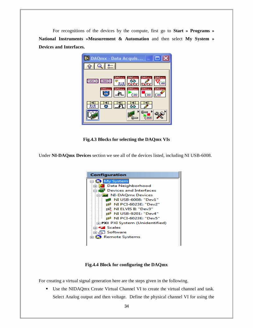
For recognitions of the devices by the compute, first go to Start » Programs »
National Instruments »Measurement & Automation and then select My System »
Devices and Interfaces.
Fig.4.3 Blocks for selecting the DAQmx VIs
Under NI-DAQmx Devices section we see all of the devices listed, including NI USB-6008.
Fig.4.4 Block for configuring the DAQmx
For creating a virtual signal generation here are the steps given in the following.
Use the NIDAQmx Create Virtual Channel VI to create the virtual channel and task.
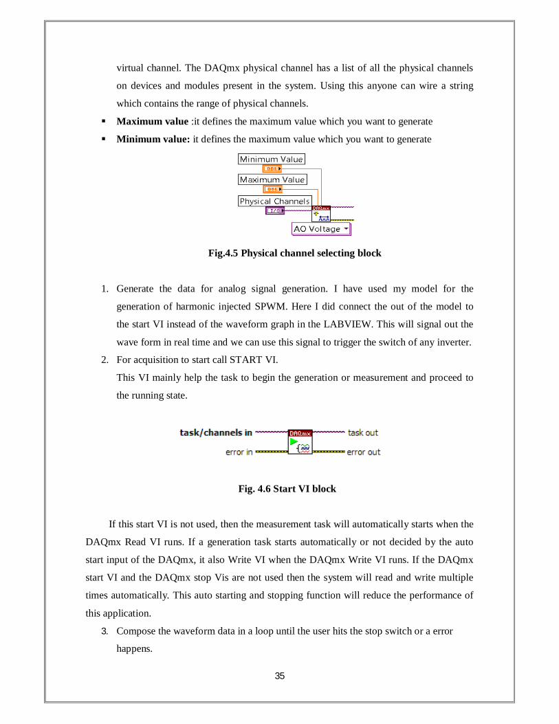
Select Analog output and then voltage. Define the physical channel VI for using the
35
virtual channel. The DAQmx physical channel has a list of all the physical channels
on devices and modules present in the system. Using this anyone can wire a string
which contains the range of physical channels.
Maximum value :it defines the maximum value which you want to generate
Minimum value: it defines the maximum value which you want to generate
Fig.4.5 Physical channel selecting block
1. Generate the data for analog signal generation. I have used my model for the
generation of harmonic injected SPWM. Here I did connect the out of the model to
the start VI instead of the waveform graph in the LABVIEW. This will signal out the
wave form in real time and we can use this signal to trigger the switch of any inverter.
2. For acquisition to start call START VI.
This VI mainly help the task to begin the generation or measurement and proceed to
the running state.
Fig. 4.6 Start VI block
If this start VI is not used, then the measurement task will automatically starts when the
DAQmx Read VI runs. If a generation task starts automatically or not decided by the auto
start input of the DAQmx, it also Write VI when the DAQmx Write VI runs. If the DAQmx
start VI and the DAQmx stop Vis are not used then the system will read and write multiple
times automatically. This auto starting and stopping function will reduce the performance of
this application.
3. Compose the waveform data in a loop until the user hits the stop switch or a error
happens.

36
Fig.4.7 Write VI block
4. Create a while loop and set up shift registers for both task and error cluster from the
NI DAQmx start VI. Add a wait VI (in Timing) and connect 200 to its input. Right
click the conditional terminal and create a control named stop. Extract the error status
using the “unbundled cluster by name” function in Cluster and variants. The
output from this function should be OR’ed with the signal from the stop button inside
the loop. This can control the application to stop if any error occurs during the
generation of the signal.
5. Connect the NI-DAQmx VIs through “task in” and “task out” terminals and error
cluster input and output terminals. At the error output of “NI-DAQmx Is Task Done”
VI extract the error status using the “unbundled cluster by name” function. The output
from this function should be ORed with the signal from the stop button inside the
loop. This can control the application to stop if any error occurs during the generation
of the signal.
6. Drop the “NI-DAQmx Clear VI” to the block diagram outside of the while loop.
7. Drop a “Simple Error Handler VI in Dialog and user interface” to the block diagram
and connect the error output of the “NI-DAQmx Clear VI” to it.
8. Launch your data acquisition VI. Run both data acquisition VI and signal generation
VI. You should be able to collect the generated signal.
5. Lab view schematic
Fig.4.8 (a) Schematic representation for simple SPWM
37
Fig.4.8 (b) Lab view schematic for harmonic injected modulation
6. OUTPUT RESULT
Fig 4.9 (a) Message signal from Lab view
Fig 4.9(b) carrier signal from Lab view
38
Fig.4.9(c) SPWM from LAB view
Fig 4.9(d) Harmonic injected sine wave
Fig.4.9 (e) SPWM from harmonic injected sine wave
39
DAQmx blocks for real time signal acquiring
Fig.4.10 Blocks of DAQmx VIs for the real time generation of SPWM

40
Chapter-5
41
1. Conclusion
Here we had discussed about various techniques for the generation of the SPWM firing
pulse of a Single phase inverter. Every method had its own limits. In the first method
Simulink incorporated with the Arduino Uno, the frequency of the modulated wave is limited
up to 1 kHz only. If we further increase the frequency of carrier wave, the signal gets
distorted due to the mismatch between the Baud rate of Arduino cycle and rate of data
transfer from the Matlab. In the second method, although we able to get desired sampling
frequency there is some undesired time gap between two cycles of SPWM due to the pre-
settings of the Arduino Uno, which will also effect on the outputs of the inverter. In the last
method generating SPWM/harmonics injected SPWM with lab view it is easy. But for the
real time firing of the inverter circuit, need to take out the signal using DAQmx block in
LabVIEW for continuous sampling.
2. Future scope
In the future we can apply the generated SPWM signals to fire the inverter circuits.
By improvisation we also can generate a higher frequency SPWM and reduce the
harmonics in the inverter circuit.
By reducing the unwanted time gap in the SPWM signal, generated from Arduino
board can be removed for the betterment and it will ease to control the output signal
of the inverter circuit.

42
References
[1]. Ming Li, Dong Dai & Xikui Ma, "Slow-Scale and Fast-Scale Instabilities in Voltage-
Mode Controlled Full-Bridge Inverter" Journal: Circuits Systems and Signal Processing -
CIRC SYST SIGNAL PROCESS , vol. 27, no. 6, pp. 811-831, 2008.
[2]. Maswood. Ali.I & Al-Ammar. Essam "Analysis of a PWM Voltage Source Inverter with
PI Controller under Non-ideal conditions" International Power Engineering Conference-
IPEC,2010.
[3]. Anand. D & Jeevananthan .S "Modeling and Analysis of Conducted EMI Emissions of
a Single-Phase PWM Inverters" Asian Power Electronics Journal, Vol. 4, No.3 December
2010.
[4]. Crowley. Ian. F & Leung. H. F "PWM Techniques: A Pure Sine Wave Inverter"
Worcester Polytechnic Institute Major Qualifying Project, 2010.
[5]. Kim. J, Choi. J & Hong. H, "Output LC Filter Design of Voltage Source Inverter
Considering the Performance of Controller" IEEE Conference Publications, 2000.
[6]. Lin.W.Song & Huang.I.Bau “Harmonic Reduction in Inverters by Use of Sinusoidal
Pulse Width Modulation” IEEE Transactions on Industrial Electronics - IEEE TRANS IND
ELECTRON , vol. IECI-27, no. 3, pp. 201-207, 1980
[7]. LU H F. A method of producing SPWM control waveform DSP-based[J]. Mechanical &
Electrical Engineering Magazine, 2002,19(5):30-34
[8]. SUN X. Preliminary analysis on single-phase asynchronous motor speed regulating[J].
Micro & Special Motor, 2005,33(1):38-40.
[9]. CHEN J H, HUANG H Q. The realization of SPWM based on DSP[J]. Equipment
Manufacturing Technology, 2009 (4):45-46.
43
[10]. BogdanM., PanuM., ViorelA., Teaching data acquisition on a virtual laboratory, the
4thBalkan Region Conference on Engineering Education, ISSN 1843-6730, 12-14 Iulie,
Sibiu, 2007.
[11]. Bogdan, M., Measurement experiment, using NI USB-6008 data acquisition, Journal of
Electrical and Electronics Engineering, Vol.2, Nr.1, 2009,ISSN 1844-6035, University of
Oradea Publisher, 2009.
[12].Bogdan, M., Sampling rate and aliasing on a virtual laboratory, Journal of Electrical and
Electronics Engineering, Vol.2, Nr.2, 2009, ISSN 1844-6035, University of Oradea
Publisher, 2009.
[13]. Bogdan, M., Virtual instrument, for frequency measurement and spectral analysis,
Journal of Electrical and Electronics Engineering ISSN/ EISSN: 18446035 20672128 Year:
2011 Volume: 4 Issue: 1 Pages: 19-22.
[14]. National Instruments LabVIEW Graphical Programming Course, 2007.
[15]. A quick guide to NI USB-6008/6009 I/O device, available at: http: //techteach.no/
publications/labview.
[16]. Gole.A.M “Harmonic Elimination in SPWM Inverter"1994, Halifax, Canada.
[17]. Rashid. M.H, “Power Electronics circuits devices and applications”, PHI 3rd
edition,2004 edition, New Delhi.
[18]. Bimbhra .P.S "Power Electronics" Khanna Publishers, New Delhi, 2003. 4th Edition
[19]. Mohan.N, Undeland.T &Robbins.W, “Power Electronics Converters applications and
design” 2nd edition, John Willey & sons, Singapore.