Embed Size (px)
Citation preview

HAL Id: hal-02178404https://hal.univ-lorraine.fr/hal-02178404
Submitted on 23 Oct 2020
HAL is a multi-disciplinary open accessarchive for the deposit and dissemination of sci-entific research documents, whether they are pub-lished or not. The documents may come fromteaching and research institutions in France orabroad, or from public or private research centers.
L’archive ouverte pluridisciplinaire HAL, estdestinée au dépôt et à la diffusion de documentsscientifiques de niveau recherche, publiés ou non,émanant des établissements d’enseignement et derecherche français ou étrangers, des laboratoirespublics ou privés.
Design and modeling of an equalizer for fuel cell energymanagement systems
Milad Bahrami, Jean-Philippe Martin, Gaël Maranzana, Serge Pierfederici,Mathieu Weber, Farid Meibody-Tabar, Majid Zandi
To cite this version:Milad Bahrami, Jean-Philippe Martin, Gaël Maranzana, Serge Pierfederici, Mathieu Weber, et al..Design and modeling of an equalizer for fuel cell energy management systems. IEEE Transac-tions on Power Electronics, Institute of Electrical and Electronics Engineers, 2019, 158, pp.1-1.10.1109/TPEL.2019.2899150. hal-02178404

0885-8993 (c) 2018 IEEE. Personal use is permitted, but republication/redistribution requires IEEE permission. See http://www.ieee.org/publications_standards/publications/rights/index.html for more information.
This article has been accepted for publication in a future issue of this journal, but has not been fully edited. Content may change prior to final publication. Citation information: DOI 10.1109/TPEL.2019.2899150, IEEETransactions on Power Electronics
IEEE TRANSACTIONS ON POWER ELECTRONICS
Abstract—During the lifespan of a Polymer Electrolyte Membrane Fuel Cell (PEMFC) system, some heterogeneities between the cells constituting the stack can appear. The voltage of one particular cell in a stack may decrease because of specific aging or local malfunctioning such as drying. As a result, more heat is generated in this cell leading to an increase in its temperature and thus an additional voltage loss. This snowball effect can result in the failure of the cell. Therefore, the lifetime of a PEMFC stack can be increased by applying energy management to its cells. Notable that the output voltage of a cell is lower than a stack. Hence, a high conversion ratio converter is necessary to implement such energy management. An efficient way to increase the output voltage is to connect the output capacitors of the converters such as the boosts in series. Ensuring the converters’ controllability is a key point to implement energy management. In this paper, an equalizer system is proposed to ensure the controllability of the boost converters. The balancing speed and the low number of switches are the main advantages of this system. The validity of the proposed system is verified through simulation and experiments.
Index Terms—Controllability, converter, energy
management, equalizer, Polymer Electrolyte Membrane Fuel Cell (PEMFC).
I. INTRODUCTION
URABILITY enhancement of Polymer Electrolyte
Membrane Fuel Cells (PEMFCs) is one of the major
challenges to enable the diffusion of this technology in the
mass market. In a stack, different cells are electrically
connected in series to increase the output voltage, whereas they
are supplied with gas in parallel. The whole system lifetime
strongly depends on each cell in such a connection. Therefore,
energy management can have a key role to compensate for the
faults that occurred in each cell. As an example, if the current
production by one particular cell could be decreased to mitigate
local flooding or could be increased to mitigate a local drying,
the electrochemical stability of the stack would be improved. In
the same way, if a faulty cell could be short-circuited, the stack
may continue to operate in degraded mode and ensure the
network reliability. Based on the new patent [1], the current of
any number of cells in a single stack is accessible. As a result,
the behavior of the cells in a stack can be checked and their fault
can be compensated. However, a high voltage conversion ratio
DC-DC converter is required in this case, because the number
of cells in series is decreased. Isolated or high voltage ratio step-
up DC-DC converters can be used but the basic challenge is
efficiency improvement [2], [3].
An efficient way to solve these issues is the series connection
of the DC-DC converters’ output capacitors. This solution leads
to an increase the freedom degree in management and control
of the PEMFCs. The basic drawback of this structure is the
possibility of the controllability loss. For instance, if the input
power of one cell becomes lower than the required amount, the
voltage of the corresponding capacitor will decrease. In this
case and assuming that the DC-DC converter is a boost
converter, the controllability will be lost if the output voltage
becomes lower than the input voltage. In such conditions, a
voltage equalizer or a balancing system can ensure the
controllability.
The equalizer in the literature can be categorized into two
basic groups: with an auxiliary source and without auxiliary
source [4]. The equalizers with auxiliary source use another
source to compensate the lower voltage cells. These equalizers
are not efficient, especially for embedded applications. As seen
in Fig. 1, the equalizers without auxiliary sources, are
categorized into two basic groups: dissipative and non-
dissipative equalizers [4]. Dissipative equalizers use resistance
to decrease the voltage of the higher voltage cells. These
equalizers waste much energy. Therefore, the efficiency is very
low. However, the low cost, simple implementation, and small
size are their advantages [5], [6]. The non-dissipative equalizers
can be divided into three groups: capacitor based [6]–[12],
converter based [4], [13]–[26] and other type equalizers [27],
[28]. A control approach is usually adopted for switches of a
specific structure to balance the voltages in the third group of
equalizers.
A number of capacitors are connected to cells by a number of
switches in the capacitor-based topologies. The cells are
periodically connected to these capacitors, and this operation
continues to the point where all the cells and capacitors reach
the same voltage. These equalizers require a numerous amount
of switches and they are not cost-effective for a large number
of cells or high power applications. In addition, these equalizers
can balance the voltages through several repeated operations.
As a result, they need much time to balance the voltages. The
maximum of the balancing current can be controlled by sizing
the capacitor capacitances. Therefore, the high efficiency in
balancing can be obtained independently of imbalance states
Design and modeling of an equalizer for fuel cell energy management systems
Milad Bahrami, Jean-Philippe Martin, Gaël Maranzana, Serge Pierfederici, Mathieu Weber, Farid
Meibody-Tabar, Majid Zandi
D

0885-8993 (c) 2018 IEEE. Personal use is permitted, but republication/redistribution requires IEEE permission. See http://www.ieee.org/publications_standards/publications/rights/index.html for more information.
This article has been accepted for publication in a future issue of this journal, but has not been fully edited. Content may change prior to final publication. Citation information: DOI 10.1109/TPEL.2019.2899150, IEEETransactions on Power Electronics
IEEE TRANSACTIONS ON POWER ELECTRONICS
[6]–[11]. The capacitors of each level of a multi-level converter
were frequently connected to next or previous level capacitors
by using the numerous amount of switch in [11]. In this
topology, the switches and capacitors in the multi-level
converter were used to balance the voltage of capacitors in each
level without adding another device. To overcome the problem
of the balancing time, the resonance phenomenon can be used.
Using the resonance in such topologies, the balancing speed can
be increased simultaneously with achieving the benefits of soft
switching [12].
The converter based equalizer can be categorized into three
groups: cell to stack equalizers [4], stack to cell equalizers [13],
[19]–[25], stack to stack equalizers[26], and cell to cell
equalizers [14]–[18].
A stack to cell equalizer with a flyback converter was used to
equalize the voltage of series lithium-Ion batteries in [23]. A
stack to stack equalizer was used in this topology to realize the
modular approach.
A forward-flyback resonant inverter was used to send energy
from the series cell to cells in [13]. A voltage multiplier circuit
was connected to cells. This circuit is used two diodes for each
cell to automatically select the lower voltage cells and send
energy to them. The required amount of switches was
minimized in this topology at a cost of lower efficiency due to
the use of two diodes for each cell. In this topology, the number
of switches is independent of the number of cells. Similar
topology with a buck converter on the primary side of the
transformer was used in [20] for photovoltaic application. The
forward-flyback converter in [13] the proposed was divided by
a bidirectional converter in [21]. Therefore, the design became
more flexible and circuit implementation was simplified. In
[24], a half-bridge converter was used on the primary side of a
transformer to send energy from the series connected cell to
lower voltage cells. A multi-stacked current doubler was
connected to the secondary side of the transformer in
connecting with cells. The number of diodes and inductances
must be increased by increasing the number of cells. Since this
topology can be implemented with two switches independent of
cells number without a multi-winding transformer, the circuit
design and implementation can be simplified. In [19], [22], an
improved push-pull converter with clamping capacitor was
used to send energy from the series cells to lower voltage cells.
A multi-winding transformer was used in this topology and H-
bridge inverters were used in the secondary windings of the
transformer. This topology needs to measure the voltage to
drive the required H-bridge inverters. The balancing current can
be very high in this topology and as a result, the balancing time
can be reduced.
For the battery applications, it is not necessary to have a large
balancing current, because the voltage difference among cells
slowly increases. Therefore, there is much time to balance the
cells with the lower current to decrease the losses [6]. However,
in such application of which the voltage balancing between
output capacitors of DC-DC converters is required to ensure the
controllability of the converters, the balancing time is the most
important parameter. On the other hand, when the difference
between cell voltages is very high, using the resonance can be
dangerous for power electronic devices due to the high current
peak. Regarding the possible inability of a cell or a set of cells
in injecting the nominal power in a stack, a large difference
between the output capacitor voltages is possible in the fuel cell
applications. As a result, a new equalizer is proposed in this
paper. The proposed equalizer can send energy to the lower
voltage cells. This topology can quickly reach the steady-state
condition by using a small number of switches and ensure the
controllability in the worst conditions. The number of
controlled switches in some converter-based equalizers
depends on the cell numbers [4], [17]–[19], [22], [23], [26].
These equalizers are not effective in term of cost and volume.
In the proposed equalizer, the number of controlled switches is
independent of the cells number. In this paper, the performance
of this equalizer is validated by the simulation and experimental
results. A state space based model is also proposed that can be
used for design purposes.
The rest of this paper is organized as follows: The principals
of the proposed equalizer and the operation modes are described
in Section II. The most important design considerations are also
summarized in this section. In Section III, the simulation results
are presented and compared with the theoretical results. The
experimental results are provided in Section IV to validate the
simulation results. Finally, conclusions are listed in Section V.
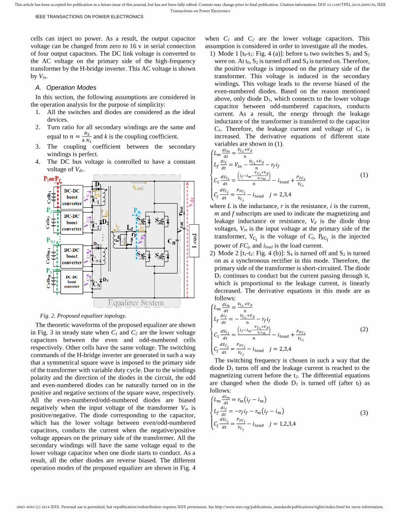
II. PROPOSED EQUALIZER
As Mentioned before, a power electronic structure is required
to manage the current of cells separately to increase the lifetime
of the stack. Since the voltage of one cell or a small number of
cells is very low, using a step-up converter is inevitable. In this
case, the conventional boost converter is used for the purpose
of simplicity. To further increase the output voltage, the output
capacitors of boost converters are connected in series. Loss of
controllability is possible in this case. To prevent this
possibility, an equalizer is proposed. The proposed power
electronic structure with the equalizer is shown in Fig. 2 where
the classic boost converters are used to connect the cells to the
DC bus. As seen in this figure, the energy can be transferred
from the series capacitors to the lower voltage capacitors. The
H-bridge inverter can send the energy to even or odd numbered
cells through the transformer. CH is a film capacitor at the input
of the H-bridge inverter to stabilize the input voltage of this
converter. The DC link voltage (Vdc) is determined by the load
requirements. Regarding the embedded application, the
standard voltage of 48 v is adopted for DC link voltage. It is
assumed that the cells inside one stack are broken down into
some group of cells with an identical number of cells.
Furthermore, it is assumed that only one group of cells has a
problem in one moment. In the worst condition, one group of
Fig. 1. Different types of equalizers.
Eq
ual
izer
s With auxiliary source
Without auxiliary source
Dissipative
Non-dissipative
Capacitor based
[6]–[12]
Converter based
[4], [13]–[26]
Other
[27], [28]
0885-8993 (c) 2018 IEEE. Personal use is permitted, but republication/redistribution requires IEEE permission. See http://www.ieee.org/publications_standards/publications/rights/index.html for more information.
This article has been accepted for publication in a future issue of this journal, but has not been fully edited. Content may change prior to final publication. Citation information: DOI 10.1109/TPEL.2019.2899150, IEEETransactions on Power Electronics
IEEE TRANSACTIONS ON POWER ELECTRONICS
cells can inject no power. As a result, the output capacitor
voltage can be changed from zero to 16 v in serial connection
of four output capacitors. The DC link voltage is converted to
the AC voltage on the primary side of the high-frequency
transformer by the H-bridge inverter. This AC voltage is shown
by Vin.
A. Operation Modes
In this section, the following assumptions are considered in
the operation analysis for the purpose of simplicity:
1. All the switches and diodes are considered as the ideal
devices.
2. Turn ratio for all secondary windings are the same and
equal to 𝑛 =𝑁2
𝑘 𝑁1 and k is the coupling coefficient.
3. The coupling coefficient between the secondary
windings is perfect.
4. The DC bus voltage is controlled to have a constant
voltage of Vdc.
The theoretic waveforms of the proposed equalizer are shown
in Fig. 3 in steady state when C1 and C2 are the lower voltage
capacitors between the even and odd-numbered cells
respectively. Other cells have the same voltage. The switching
commands of the H-bridge inverter are generated in such a way
that a symmetrical square wave is imposed to the primary side
of the transformer with variable duty cycle. Due to the windings
polarity and the direction of the diodes in the circuit, the odd
and even-numbered diodes can be naturally turned on in the
positive and negative sections of the square wave, respectively.
All the even-numbered/odd-numbered diodes are biased
negatively when the input voltage of the transformer Vin is
positive/negative. The diode corresponding to the capacitor,
which has the lower voltage between even/odd-numbered
capacitors, conducts the current when the negative/positive
voltage appears on the primary side of the transformer. All the
secondary windings will have the same voltage equal to the
lower voltage capacitor when one diode starts to conduct. As a
result, all the other diodes are reverse biased. The different
operation modes of the proposed equalizer are shown in Fig. 4
when C1 and C2 are the lower voltage capacitors. This
assumption is considered in order to investigate all the modes.
1) Mode 1 [t0-t1: Fig. 4 (a)]: before t0 two switches S1 and S2
were on. At t0, S2 is turned off and S4 is turned on. Therefore,
the positive voltage is imposed on the primary side of the
transformer. This voltage is induced in the secondary
windings. This voltage leads to the reverse biased of the
even-numbered diodes. Based on the reason mentioned
above, only diode D1, which connects to the lower voltage
capacitor between odd-numbered capacitors, conducts
current. As a result, the energy through the leakage
inductance of the transformer is transferred to the capacitor
C1. Therefore, the leakage current and voltage of C1 is
increased. The derivative equations of different state
variables are shown in (1).
𝐿𝑚
𝑑𝑖𝑚
𝑑𝑡=
𝑉𝐶1+𝑉𝑑
𝑛
𝐿𝑓𝑑𝑖𝑓
𝑑𝑡= 𝑉𝑖𝑛 −
𝑉𝐶1+𝑉𝑑
𝑛− 𝑟𝑓𝑖𝑓
𝐶1𝑑𝑉𝐶1
𝑑𝑡=
(𝑖𝑓−𝑖𝑚−𝑉𝐶1
+𝑉𝑑
𝑛 𝑟𝑚)
𝑛− 𝑖𝑙𝑜𝑎𝑑 +
𝑃𝐹𝐶1
𝑉𝐶1
𝐶𝑗𝑑𝑉𝐶𝑗
𝑑𝑡=
𝑃𝐹𝐶𝑗
𝑉𝐶𝑗− 𝑖𝑙𝑜𝑎𝑑 𝑗 = 2,3,4
(1)
where L is the inductance, r is the resistance, i is the current,
m and f subscripts are used to indicate the magnetizing and
leakage inductance or resistance, Vd is the diode drop
voltages, Vin is the input voltage at the primary side of the
transformer, VCj is the voltage of Cj, PFCj is the injected
power of FCj, and iload is the load current.
2) Mode 2 [t1-t2: Fig. 4 (b)]: S4 is turned off and S2 is turned
on as a synchronous rectifier in this mode. Therefore, the
primary side of the transformer is short-circuited. The diode
D1 continues to conduct but the current passing through it,
which is proportional to the leakage current, is linearly
decreased. The derivative equations in this mode are as
follows:
𝐿𝑚
𝑑𝑖𝑚
𝑑𝑡=
𝑉𝐶1+𝑉𝑑
𝑛
𝐿𝑓𝑑𝑖𝑓
𝑑𝑡= −
𝑉𝐶1+𝑉𝑑
𝑛− 𝑟𝑓𝑖𝑓
𝐶1𝑑𝑉𝐶1
𝑑𝑡=
(𝑖𝑓−𝑖𝑚−𝑉𝐶1
+𝑉𝑑
𝑛 𝑟𝑚)
𝑛− 𝑖𝑙𝑜𝑎𝑑 +
𝑃𝐹𝐶1
𝑉𝐶1
𝐶𝑗𝑑𝑉𝐶𝑗
𝑑𝑡=
𝑃𝐹𝐶𝑗
𝑉𝐶𝑗− 𝑖𝑙𝑜𝑎𝑑 𝑗 = 2,3,4
(2)
The switching frequency is chosen in such a way that the
diode D1 turns off and the leakage current is reached to the
magnetizing current before the t2. The differential equations
are changed when the diode D1 is turned off (after tf) as
follows:
𝐿𝑚
𝑑𝑖𝑚
𝑑𝑡= 𝑟𝑚(𝑖𝑓 − 𝑖𝑚)
𝐿𝑓𝑑𝑖𝑓
𝑑𝑡= −𝑟𝑓𝑖𝑓 − 𝑟𝑚(𝑖𝑓 − 𝑖𝑚)
𝐶𝑗𝑑𝑉𝐶𝑗
𝑑𝑡=
𝑃𝐹𝐶𝑗
𝑉𝐶𝑗− 𝑖𝑙𝑜𝑎𝑑 𝑗 = 1,2,3,4
(3)
Fig. 2. Proposed equalizer topology.

0885-8993 (c) 2018 IEEE. Personal use is permitted, but republication/redistribution requires IEEE permission. See http://www.ieee.org/publications_standards/publications/rights/index.html for more information.
This article has been accepted for publication in a future issue of this journal, but has not been fully edited. Content may change prior to final publication. Citation information: DOI 10.1109/TPEL.2019.2899150, IEEETransactions on Power Electronics
IEEE TRANSACTIONS ON POWER ELECTRONICS
3) Mode 3 [t2-t3: Fig. 4 (c)]: S1 is turned off and S3 is turned
on in this mode. The negative voltage appears on the
primary side of the transformer. In other words, Vin has a
negative value. This mode like mode 1 has the same effect
on the even numbered capacitors. The voltage of C2 is the
lowest voltage between the even-numbered capacitors.
Therefore, the diode D2 is turned on and the leakage current
and the voltage of C2 starts to increase. The leakage current
negatively increases. The derivative equations in this mode
are as follows:
𝐿𝑚
𝑑𝑖𝑚
𝑑𝑡= −
𝑉𝐶2+𝑉𝑑
𝑛
𝐿𝑓𝑑𝑖𝑓
𝑑𝑡= 𝑉𝑖𝑛 +
𝑉𝐶2+𝑉𝑑
𝑛− 𝑟𝑓𝑖𝑓
𝐶2𝑑𝑉𝐶2
𝑑𝑡= −
(𝑖𝑓−𝑖𝑚+𝑉𝐶2
+𝑉𝑑
𝑛 𝑟𝑚)
𝑛− 𝑖𝑙𝑜𝑎𝑑 +
𝑃𝐹𝐶2
𝑉𝐶2
𝐶𝑗𝑑𝑉𝐶𝑗
𝑑𝑡=
𝑃𝐹𝐶𝑗
𝑉𝐶𝑗− 𝑖𝑙𝑜𝑎𝑑 𝑗 = 1,3,4
(4)
4) Mode 4 [t3-t4: Fig. 4 (d)]: This mode is similar to mode 2
with this difference that S3 is turned off and S1 is turned on.
Before the diode D2 is turned off, the differential equations
of the system are as follows:
𝐿𝑚
𝑑𝑖𝑚
𝑑𝑡= −
𝑉𝐶2+𝑉𝑑
𝑛
𝐿𝑓𝑑𝑖𝑓
𝑑𝑡=
𝑉𝐶2+𝑉𝑑
𝑛− 𝑟𝑓𝑖𝑓
𝐶2𝑑𝑉𝐶2
𝑑𝑡= −
(𝑖𝑓−𝑖𝑚+𝑉𝐶2
+𝑉𝑑
𝑛 𝑟𝑚)
𝑛− 𝑖𝑙𝑜𝑎𝑑 +
𝑃𝐹𝐶2
𝑉𝐶2
𝐶𝑗𝑑𝑉𝐶𝑗
𝑑𝑡=
𝑃𝐹𝐶𝑗
𝑉𝐶𝑗− 𝑖𝑙𝑜𝑎𝑑 𝑗 = 1,3,4
(5)
Then, the diode D2 is turned off and the differential equations
of the system change as (4).
The power is transferred through the transformer to increase
the voltage of lower voltage capacitors. Any losses in the
transformer reduce the power that is received by lower voltage
cells. The transformer leakage inductance can also affect its
transmitting power by affecting its input current. Therefore, the
transformer design has a key role in this topology.
B. Design considerations
The magnetizing inductance of the transformer must be
maximized in order to reduce the magnetizing current. For
instance, Lm and Lf of a core with two windings can be
calculated by the following equation:
𝐿𝑚 = 𝑘2𝐿1
𝐿𝑓 = (1 − 𝑘2)𝐿1
(6)
Where k is the coupling coefficient and L1 can be calculated
by:
𝐿1 =𝑁2
ℜ (7)
N is the number of turns and ℜ is the reluctance of the core.
As seen in this equation, increasing the number of turns and
decreasing the reluctance lead to increase the magnetizing
inductance. Increasing the number of turns increases the
volume of the transformer and, therefore, increase the
hysteresis losses. Furthermore, increasing the number of turns
also increases the wire length that leads to an increase of the
wire resistance and, consequently, the copper losses. The
reluctance is inversely proportional to the permeability. Hence,
selecting a core with high permeability can make it possible to
increase the magnetizing inductance with a lower volume. This
also increases the leakage inductance. However, the leakage
inductance affects the maximum transmitting power through
the transformer in each cycle. This power is also the most
important parameter in reducing the equalizing time. To obtain
this power in steady state by considering the first group of cells
as the faulty cells, the diode current can be used to calculate the
transferred energy. Therefore, the transferred energy can be
calculated as follows:
Fig. 3. Theoretical waveforms in steady-state operation of the
proposed equalizer.
Fig. 4. Different operation modes of the proposed equalizer. (a)
Mode 1: t0<t<t1. (b) Mode 2: t1<t<t2. (c) Mode3: t2<t<t3. (d) Mode
4: t3<t<t4.

0885-8993 (c) 2018 IEEE. Personal use is permitted, but republication/redistribution requires IEEE permission. See http://www.ieee.org/publications_standards/publications/rights/index.html for more information.
This article has been accepted for publication in a future issue of this journal, but has not been fully edited. Content may change prior to final publication. Citation information: DOI 10.1109/TPEL.2019.2899150, IEEETransactions on Power Electronics
IEEE TRANSACTIONS ON POWER ELECTRONICS
𝑊𝑒 = 𝑉𝐶1 ∫ 𝑖𝐷(𝑡)𝑑𝑡𝑡𝑓𝑡0
= 𝑉𝐶1 ∫𝑖𝑓−𝑖𝑚−
𝑉𝐶1+𝑉𝑑
𝑛 𝑟m
𝑛𝑑𝑡
𝑡𝑓𝑡0
(8)
Where We is the energy that is received by the faulted cell,
𝑉𝐶1 is the voltage of the first capacitor, and iD is the
corresponding diode current that is on. Based on Fig. 3, this
equation can be solved by dividing its time interval into two
intervals:
𝑊𝑒 = (∫𝑖𝑓−𝑖𝑚
𝑛𝑑𝑡
𝑡1𝑡0
+ ∫𝑖𝑓−𝑖𝑚
𝑛𝑑𝑡
𝑡𝑓𝑡1
−𝑉𝐶1+𝑉𝑑
𝑛 𝑟m(𝑡𝑓 − 𝑡0)) (9)
Assuming that the time constant of Lf/rf is much larger than
tf-t1, the magnetizing and leakage current functions can be
obtained based on (1) in the interval [t0,t1] as follows:
𝑖𝑓(𝑡) = −𝑖𝑚0 (1 −
𝑡𝐿𝑓
𝑟𝑓
)+∑ 𝑉𝐶𝑗𝑗 −
𝑉𝑑+𝑉𝐶1𝑛
𝐿𝑓𝑡
𝑖𝑚(𝑡) = −𝑖𝑚0 +𝑉𝑑+𝑉𝐶1𝑛 𝐿m
𝑡
(10)
Where -im0 is the magnetizing current at t0. The magnetizing
current value at tf is equal to im0. keeping the same assumption
like (10) for the time constant of Lf/rf, the magnetizing and
leakage current functions can be obtained based on (2) in the
interval of [t1,tf] as follows:
𝑖𝑓(𝑡) = 𝑖𝑚0(1 −
𝑡−𝑡1𝐿𝑓
𝑟𝑓
)+𝑉𝑑+ 𝑉𝐶1
𝑛 𝐿𝑓(𝑡𝑓 − 𝑡1) −
𝑉𝑑+ 𝑉𝐶1
𝑛 𝐿𝑓(𝑡 − 𝑡1)
𝑖𝑚(𝑡) = 𝑖𝑚0 +𝑉𝑑+𝑉𝐶1
𝑛 𝐿m(𝑡 − 𝑡𝑓)
(11)
Thus, by solving (9), a function for the transferred energy is
obtained based on Lf, Lm, m, Vd, tf-t1, t1-t0, VC1, and the sum of
the capacitor voltages. The interval t1-t0 is equal to dT/2 where
T=1/F and F is the switching frequency of the H-bridge
inverter, and d is its duty cycle. The value of tf-t1 can be
calculated by writing the diode current equation over this
interval [t1,tf]. The diode current can be obtained from
integrating the following equation: 𝑑𝑖𝐷
𝑑𝑡=
𝑑𝑖𝑓
𝑑𝑡−𝑑𝑖𝑚
𝑑𝑡−𝑉𝐶1+𝑉𝑑
𝑛 𝑟𝑚 (12)
Integration of this equation in the interval of t0-t1 and using
(10), an equation is obtained for the maximum current value of
the diode. Another equation for the maximum current of the
diode can be obtained by integrating (12) in the interval of t1-tf
and using (11). The time tf-t1 can be calculated by solving these
two equations.
To eliminate im0 from the equations, the equation of
magnetizing current over the whole interval [t0,tf] can be used
as follows:
𝑖𝑚0 = −𝑖𝑚0 +𝑉𝑑+𝑉𝐶1
𝑛 𝐿m(𝑡1 − 𝑡0) → 2𝑖𝑚0 =
𝑉𝑑+𝑉𝐶1
𝑛 𝐿m(𝑡1 − 𝑡0) (13)
A function for the transferred energy is obtained by replacing
(10) and (11) in (9) and using (12) and (13). The transmitting
power through the transformer can be calculated with respect to
this energy using the following equation:
𝑃𝑒 =𝑑𝑉𝐶1
8𝐹2𝑛2(𝑑𝐹(𝑛𝑉𝑑𝑐−(𝑉𝐶1+𝑉𝑑))
𝐿𝑓−𝑑𝐹(𝑉𝐶1+𝑉𝑑)
𝐿𝑚−
16𝐹3𝐿𝑚(𝑛𝑟𝑚𝑉𝑑𝑐−2𝐿𝑓(𝑉𝐶1+𝑉𝑑))
𝑟𝑚(−4𝐹𝐿𝑓𝐿𝑚+4𝐹(𝐿𝑓+𝐿𝑚)𝑟𝑚−𝑑𝑟𝑓𝑟𝑚)+
𝑑2𝐹𝑟𝑓(−𝑛𝑟𝑚𝑉𝑑𝑐+2𝐿𝑓(𝑉𝐶1+𝑉𝑑))
𝐿𝑓(4𝐹𝐿𝑓𝐿𝑚−4𝐹(𝐿𝑓+𝐿𝑚)𝑟𝑚+𝑑𝑟𝑓𝑟𝑚)−
𝑑(−4𝐹(𝐿𝑓+𝐿𝑚)+𝑑𝑟𝑓+𝑑𝑟𝑓)
4𝐿𝑓𝐿𝑚(4𝐹𝐿𝑓𝐿𝑚−4𝐹(𝐿𝑓+𝐿𝑚)𝑟𝑚+𝑑𝑟𝑓𝑟𝑚)2(𝑉𝐶1+𝑉𝑑)
(4𝐹𝐿𝑚𝑟𝑚 (𝑛𝑉𝑑𝑐 − (𝑉𝐶1 +
𝑉𝑑)) + 𝑑𝑟𝑓𝑟𝑚(𝑉𝐶1 + 𝑉𝑑) − 4𝐹𝐿𝑓(𝐿𝑚 + 𝑟𝑚)(𝑉𝐶1 + 𝑉𝑑))2
) (14)
As seen in this equation, the transferred power in steady state
depends on the leakage and magnetizing inductances, capacitor
voltages, frequency, duty cycle, iron losses, copper losses, and
transformer turn ratio.
With the hypothesis that only one diode between odd-
numbered cells/ even-numbered cells can be turned on at the
positive/negative part of the input voltage of the transformer,
the voltage difference can be calculated. In this case, just the
first cell is supposed to have a problem. For this purpose, the
Kirchhoff current law in steady state for each capacitor is
written as follows:
𝑃1+𝑃𝑒
𝑉𝐶1− 𝑖𝑙𝑜𝑎𝑑 = 0
𝑃𝑗
𝑉𝐶𝑗− 𝑖𝑙𝑜𝑎𝑑 = 0 ∀ 𝑗 ∈ 2, 3 , … , 𝑛
(15)
where 𝑉𝐶𝑗is the voltage of capacitor number j, Pj is the supplied
power by the cell number j, and iload is the load current. The
equation of load current is as follows:
𝑖𝑙𝑜𝑎𝑑 =𝑃𝑖𝑛
𝑉𝑑𝑐+𝑉𝑑𝑐−𝑉𝑏𝑎𝑡
𝑟𝑏𝑎𝑡 (16)
where Vdc is the DC bus voltage that is controlled to have a
constant value, Vbat and rbat is the voltage and the resistance of
the power supply respectively that controls the DC bus voltage,
and Pin is the power injected to the equalizer system as follows:
𝑃𝑖𝑛 = 𝑃𝑒 +𝑉𝑝2
𝑟𝑚+ 𝑟𝑓(𝐼)
2 (17)
where 𝐼 is the RMS value of leakage current that can be calculated
using (10) and (11), and 𝑝 is the RMS voltage on the primary side of
the transformer that is the RMS value of 𝑉𝑑+ 𝑉𝐶1
n over the interval of tf-
t0 in the switching period as follows:
𝐼2=
1
𝑇∫ (𝑖𝑓(𝑡))
2𝑑𝑡
𝑡𝑓𝑡0
=1
𝑇(∫ (𝑖𝑓(𝑡))
2𝑑𝑡
𝑡1𝑡0
+ ∫ (𝑖𝑓(𝑡))2𝑑𝑡
𝑡𝑓𝑡1
)
𝑝2=
1
𝑇∫ (
𝑉𝑑+ 𝑉𝐶1
𝑛 )2𝑑𝑡
𝑡𝑓𝑡0
=(𝑡𝑓−𝑡0)
𝑇(𝑉𝑑+ 𝑉𝐶1
𝑛 )2 (18)
By substituting (16) and (14) in (15), the resulting equations
form a system of equations. 𝑉𝐶𝑗 can be determined by solving
this system numerically. Then, Pe can be calculated by (14).
The results of these theoretical equations are shown in Fig. 5 by
assuming the four capacitors in series, and that all PEMFCs can
inject the rated power of 126 W except FC1 that injects no
power. Other information is summarized in TABLE I.
Therefore, the corresponding capacitor voltage (𝑉𝐶1) is
decreased. To investigate the impact of the leakage inductance
on the transferred power to the lower voltage capacitor, the duty
Fig. 5. The amount of transferred power through the transformer
of the proposed equalizer in steady state based on: (a) Changes in
the amount of leakage inductance when the duty cycle of H-bridge
inverter is equal to 0.4. (b) Changes in the amount of supplied power
by the faulted cell and changes in the duty cycle.

0885-8993 (c) 2018 IEEE. Personal use is permitted, but republication/redistribution requires IEEE permission. See http://www.ieee.org/publications_standards/publications/rights/index.html for more information.
This article has been accepted for publication in a future issue of this journal, but has not been fully edited. Content may change prior to final publication. Citation information: DOI 10.1109/TPEL.2019.2899150, IEEETransactions on Power Electronics
IEEE TRANSACTIONS ON POWER ELECTRONICS
cycle of the H-bridge inverter is assumed to be 0.6 and the
leakage inductance is changed. Using (14)-(16), the transferred
power is calculated for different value of the leakage
inductance. The amount of transferred power as a function of
the leakage inductance is shown in Fig. 5 (a). As seen in this
figure, the amount of power is decreased by increasing the
leakage inductance. Thus, the leakage inductance should be
minimized in one hand. A large leakage inductance is required
to limit the overshoot of the current in another hand. Therefore,
there must be a trade-off between the peak of current and
maximum transferred power through the transformer.
To check the effectiveness of the proposed equalizer, it is
assumed that the first group of cells cannot inject the nominal
power. The injected power by the first cell is changed from zero
to nominal power. The other groups of cells inject the nominal
power. In this condition, the transferred power is calculated by
changing the duty cycle of the H-bridge inverter based on (14)-
(16). The transferred power by changing the duty cycle of the
H-bridge inverter for different value of first cells injected power
is shown in Fig. 5 (b). As seen in this figure, the further
reduction in injected power by the first group of cells can be
compensated by increasing the duty cycle of the H-bridge
inverter. In other words, the transferred power through the
transformer is increased by increasing the duty cycle of the H-
bridge inverter when the injected power of faulted cell was
decreased.
To select a magnetic core based on the constraints mentioned
above, the worst condition is taken into account. In this
condition, one group of cells should be short-circuited. Thus,
one group can inject no power while the other groups inject the
nominal power. In this condition, the output voltage of the boost
converter connected to the faulted cell decreased and the
controllability is lost. The equalizer should send the power to
this capacitor to ensure the controllability. The Leakage
inductance of the transformer has an impact on the primary and
secondary transformer side currents. Considering the first group
of cells as the faulted cells, the first capacitor voltage is equal
to zero in this condition. As a result and based on (10) and (13),
the leakage current in transient conditions can be calculated as
follows:
𝑖𝑓 =∑ 𝑉𝐶𝑗𝑗
𝐿𝑓𝑡 (19)
The DC link voltage is controlled to have a constant value of
48 V and based on Fig. 3, the maximum of the leakage current
can be calculated as follows:
𝑖𝑓𝑚𝑎𝑥=
48
𝐿𝑓
𝑑𝑇
2 (20)
Using (10), (12), and (13), the maximum current of the diode
can be calculated as follows:
𝑖𝐷𝑚𝑎𝑥 =48
𝐿𝑓
𝑑𝑇
2𝑛 (21)
In the worst case, the duty cycle is equal to the maximum
value of one. The maximum of the leakage current in the
transient conditions for different value of the leakage
inductance is shown in Fig. 6. As seen in this figure, the peak
of the leakage current is very high. Indeed, a low-pass filter can
cope with this problem and control the rate of duty-cycle
change.
The leakage current in steady-state can be used to make a
decision about the rating of the semiconductor devices.
Considering a proportional gain to control the duty cycle of the
H-bridge inverter in closed-loop, the maximum of the leakage
and diode currents can be calculated by (10) and (12)-(16).
These currents are shown in Fig. 7 by changing the leakage
inductance of the transformer when the first group of cells can
inject no power and other groups can inject the nominal power.
As seen in this figure, if the leakage inductance is equal to 5 µF,
the current rating of the H-bridge inverter switches should be
very higher than 15 A and the current rating of the diodes should
be higher than 60 A. Therefore, there is a trade-off between the
current rating of the semiconductor devices and the maximum
power that can be transferred through the transformer.
The coupling coefficient of 0.99 is assumed based on previous
experiences. Replacing (6) in (14) and using (15) and (16), the
value of L1 can be calculated to send the nominal power by the
equalizer. Equation (7) can be used to select the magnetic core
by knowing L1. It is essential to minimize the volume of the
transformer to reduce its losses. Therefore, the desired core can
be chosen among the magnetic core in the market by using (7)
and the classical equation of the minimum number of turns with
the aim of minimizing the transformer volume. Considering
these design constraints, the devices used to make simulation
and obtain experimental results are shown in TABLE I.
III. SIMULATION RESULTS
A simulation is made by four capacitors in series in Matlab
Simulink to preliminary verify the validity of the proposed
equalizer theories. For a precise study of the balancing system,
the H-bridge inverter is controlled in the open-loop mode and
duty cycle is set to 0.4. It is assumed that the PEMFCs
connected to the first and second capacitors can inject the half
of nominal power and the other cells inject the nominal power
Fig. 6. Impact of the leakage inductance on the maximum of
leakage current in transient conditions.
Fig. 7. Impact of the leakage inductance on a) the maximum of
leakage current b) the maximum of the diode current in steady state.
0885-8993 (c) 2018 IEEE. Personal use is permitted, but republication/redistribution requires IEEE permission. See http://www.ieee.org/publications_standards/publications/rights/index.html for more information.
This article has been accepted for publication in a future issue of this journal, but has not been fully edited. Content may change prior to final publication. Citation information: DOI 10.1109/TPEL.2019.2899150, IEEETransactions on Power Electronics
IEEE TRANSACTIONS ON POWER ELECTRONICS
(126 W). The voltage and current waveforms on the primary
side of the transformer for d=0.4 are shown in Fig. 8. As seen
in this figure, the current is linear and the power can be
transmitted through the transformer. These results are also in
agreement with the theoretical waveforms.
To control the duty cycle of the H-bridge inverter in closed-
loop, a simple proportional control is used. This closed-loop
proportional control is implemented by comparing the average
voltage of capacitors and their minimum voltage. As seen in
Fig. 9, a low-pass filter is used in this control to limit the
maximum current in transient conditions. The low pass filter is
designed by considering the worst condition (short circuit of
one group of cells) to ensure that the leakage current has no
overshoot during transient conditions. The cut-off frequency of
this filter is equal to 10 rad/s. The proportional gain (P) of this
controller is set to 0.1 for the purpose of simulation and
experimental results. The voltage changes of different
capacitors with this closed-loop controller are shown in Fig. 10
when the cells inject nominal power except the first cell. The
first cell is turned off and it can inject no power in this
simulation.
IV. EXPERIMENTAL RESULTS
For further verify the proposed balancing system and
validation of the theoretical analysis and simulation, the
experiments are conducted on a laboratory prototype as
demonstrated in Fig. 11. dSPACE 1005 with FPGA board is
used to receive the information and send the commands. Four
programmable power supplies are used to emulate the
PEMFCs. These power supplies are connected to four boost
converters, the output capacitors of the boosts are connected in
series. The component part number used in this prototype are
listed in Table II. The proposed balancing system connects to
these capacitors. It is notable that a planar transformer is built
for this paper. Each winding turn of this transformer means a
printed circuit board. On each printed circuit board, a copper
line with the width of 21.5 mm and the thickness of 35 µm is
rotated in such a way that the circuits can be placed in the
window of the magnetic core. This design is used to minimize
the leakage inductance. The turn number of primary and
secondary windings are shown in Table I.
To check the validity of the theoretical analysis and
simulation, several experiments have been accomplished. First
experiment conditions are similar to the first simulation. The
cells inject nominal power except first and second cells. These
cells inject the half of nominal power. The voltage and current
waveforms on the primary side of the transformer for d=0.4 are
shown in Fig. 12. As seen in this figure, the results are in
agreement with the simulation results and the power can be
transferred to the first and second capacitors during the positive
and negative part of the input voltage respectively.
The second experiment conditions are similar to the second
simulation. The first power supply is turned off and as a result,
it can inject no power. The other cells inject the nominal power.
The voltage changes of different capacitors are shown in Fig.
13 when the duty-cycle of H-bridge inverter is controlled in
closed-loop with the same parameter of simulation
.
To validate the proposed model for the design purpose, the
capacitor voltages are measured when the first cell can inject
the half of nominal power. In this experiment, the duty cycle is
changed in the open-loop from 0.3 to 0.9. These voltages are
also numerically calculated by (14)-(16). The output power of
each boost converter is measured. These powers are used in
these theoretical equations. The results of the experiment and
theoretical equations are shown in Table III. In this table, the
error 𝑉𝐶1 is the relative error of the first capacitor voltage. In
this table, the error is the root mean square of the relative errors
as follows:
𝐸𝑟𝑟𝑜𝑟 = √∑ (𝑉𝐶𝑗𝑡ℎ
−𝑉𝐶𝑗𝑒𝑥𝑝
𝑉𝐶𝑗𝑡ℎ
)
2
4𝑗=1 (22)
where 𝑉𝐶𝑗𝑡ℎ and 𝑉𝐶𝑗𝑒𝑥𝑝
are respectively the theoretical and
experimental voltage of the jth capacitor.
Fig. 8. Simulation results of voltage and current waveforms on
the primary side of the transformer for d=0.4.
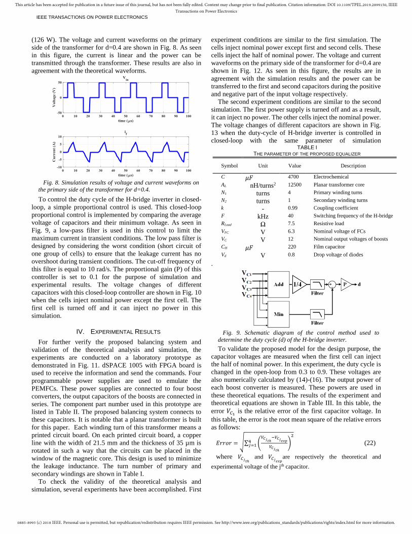
TABLE I THE PARAMETER OF THE PROPOSED EQUALIZER
Symbol Unit Value Description
C 𝜇𝐹 4700 Electrochemical
AL nH/turns2 12500 Planar transformer core
N1 turns 4 Primary winding turns
N2 turns 1 Secondary winding turns
k - 0.99 Coupling coefficient
F kHz 40 Switching frequency of the H-bridge
RLoad Ω 7.5 Resistive load
VFC V 6.3 Nominal voltage of FCs
VC V 12 Nominal output voltages of boosts
CH 𝜇𝐹 220 Film capacitor
Vd V 0.8 Drop voltage of diodes
Fig. 9. Schematic diagram of the control method used to
determine the duty cycle (d) of the H-bridge inverter.

0885-8993 (c) 2018 IEEE. Personal use is permitted, but republication/redistribution requires IEEE permission. See http://www.ieee.org/publications_standards/publications/rights/index.html for more information.
This article has been accepted for publication in a future issue of this journal, but has not been fully edited. Content may change prior to final publication. Citation information: DOI 10.1109/TPEL.2019.2899150, IEEETransactions on Power Electronics
IEEE TRANSACTIONS ON POWER ELECTRONICS
The main objective of the proposed equalizer system is to
guarantee the controllability of DC-DC converters connected to
fuel cells for applying energy management (Fig. 2). The drying
and flooding conditions are the most critical conditions for the
membrane of the PEMFC. In these conditions, the energy
management system must function properly to compensate the
faults. If one cell suffers from drying, it should be short-
circuited to produce more water by keeping constant gas flow
rates. This leads to a decrease in gas stoichiometry for this
particular cell and a consequent membrane humidification. On
the contrary, no current should be generated by a cell in
flooding conditions in order to let it dry. In other words, the
power generated by the cell should be controlled near zero. In
the following, it is assumed that the first cell experiences these
conditions among four other healthy cells.
The capacitor voltages are shown in Fig. 14 (a) and the
transformer voltage and current on the primary side are shown
in Fig. 14 (b) in the flooding condition of the first PEMFC. As
seen in these figures, the current of the first PEMFC cannot be
set to zero before running the equalizer system. As seen in Fig.
14, when the square wave voltage is supplied on the primary
side of the transformer by the H-bridge inverter, the current of
the first PEMFC reaches to zero after about 40 ms with the used
Fig. 10. Simulation results of the Output capacitor voltages in closed-
loop when the first group of cells injects no power.
Fig. 11. Proposed equalizer test bench.
TABLE II COMPONENT PART NUMBER FOR PROTOTYPE.
Component Part number
FC Power supply TDK GENH 750W
Boost
converter Inductance (1mH)
Switches IGBT
Capacitor Electrochemical (4700𝜇𝐹)
Equalizer Diodes DSS2x121-0045B Magnetic core B66295G Material N87
H-bridge
switches
SiC MOSFET
CCS050M12CM2
Capacitor film (220 𝜇𝐹)
TABLE III
CAPACITOR VOLTAGES (V) COMPARISON BETWEEN THE THEORY AND
EXPERIMENT.
Duty cycle 0.3 0.4 0.5 0.6 0.7 0.8 0.9
𝑉𝐶1𝑡ℎ 10.05 10.58 10.92 11.13 11.28 11.38 11.46
𝑉𝐶2𝑡ℎ 12.72 12.54 12.43 12.35 12.31 12.27 12.25
𝑉𝐶3𝑡ℎ 12.32 12.14 12.04 11.97 11.92 11.89 11.86
𝑉𝐶4𝑡ℎ 12.92 12.74 12.63 12.55 12.51 12.47 12.44
𝑉𝐶1𝑒𝑥 10 10.5 10.9 11.1 11.3 11.3 11.4
𝑉𝐶2𝑒𝑥 12.7 12.5 12.3 12.2 12.2 12.1 12.1
𝑉𝐶3𝑒𝑥 12.4 12.1 12 12 12 12 12
𝑉𝐶4𝑒𝑥 13 12.8 12.6 12.5 12.5 12.4 12.4
Error (%) 1.04 1.00 1.14 1.33 1.13 1.89 1.81
Error 𝑉𝐶1 (%) 0.50 0.76 0.18 0.27 0.18 0.70 0.52
Fig. 12. Experimental waveforms of the current and voltage on the
primary side of the transformer when first and second fuel cells inject
the half of nominal power and duty cycle of H-bridge inverter is
equal to 0.4.
Fig. 13. Experimental results of the Output capacitor voltages
when the first group of cells injects no power.

0885-8993 (c) 2018 IEEE. Personal use is permitted, but republication/redistribution requires IEEE permission. See http://www.ieee.org/publications_standards/publications/rights/index.html for more information.
This article has been accepted for publication in a future issue of this journal, but has not been fully edited. Content may change prior to final publication. Citation information: DOI 10.1109/TPEL.2019.2899150, IEEETransactions on Power Electronics
IEEE TRANSACTIONS ON POWER ELECTRONICS
parameters for the controller. Indeed, the boost converter
connected to the first PEMFC will be controllable after this
time. Furthermore, the capacitor voltage connected to the first
PEMFC is increased and other capacitor voltages are decreased.
The output capacitor voltages of the boost converters in the
drying condition of the first PEMFC are shown in Fig. 15 (a).
In this condition, the voltage and current on the primary side of
the transformer are also shown in Fig. 15 (b). As seen in this
figure, the first capacitor voltage is increased from zero to 8
volts but the short-circuit conditions are maintained for the first
PEMFC. For this experiment, the maximum current of the
power supply is limited to 20A.
V. CONCLUSION
In this paper, an equalizer based on the multi-winding
transformer was proposed to ensure the controllability of boost
converters in a series connection of their output capacitors.
This equalizer can be used to implement the PEMFC energy
management system. The validation of the proposed system
was investigated through the simulation and experimental
results. The validity of the theoretical model was confirmed
using the experimental results. Therefore, this model can be
used to predict the behavior of the equalizer system. In other
words, the theoretical equations can be used for sizing the
system. The experimental results confirm the effectiveness of
the equalizer system in maintaining the control ability of the
boost converters when a cell is not able to supply the nominal
power. The performance of the system was also evaluated in
two critical conditions of the fuel cell operation. In both
operation conditions (emulation of drying and flooding
conditions), the controllability of the converter connected to the
faulty cell is ensured by increasing its capacitor voltage.
REFERENCES
[1] G. Maranzana, S. Didierjean, J. Dillet, A. Thomas, and O. Lottin,
“IMPROVED FUEL CELL. Patent n° : WO/2014/060198.,” 2014. [2] T. Arunkumari and V. Indragandhi, “An overview of high voltage
conversion ratio DC-DC converter configurations used in DC micro-
grid architectures,” Renew. Sustain. Energy Rev., vol. 77, no. March, pp. 670–687, 2017.
[3] A. Shahin et al., “High Voltage Ratio DC – DC Converter for Fuel-
Cell Applications,” IEEE Trans. Ind. Electron., vol. 57, no. 12, pp. 3944–3955, 2010.
[4] A. M. Imtiaz, S. Member, and F. H. Khan, “‘ Time Shared Flyback
Converter ’ Based Regenerative Cell Balancing Technique for Series Connected Li-Ion Battery Strings,” IEEE Trans. power Electron.,
vol. 28, no. 12, pp. 5960–5975, 2013.
[5] A. Hijazi, A. Sari, X. Lin-shi, and P. Venet, “Balancing Circuit New Control for Supercapacitor Storage System Lifetime Maximization,”
IEEE Trans. Power Electron., vol. 32, no. 6, pp. 4939–4948, 2017.
[6] Y. Shang, B. Xia, J. Yang, C. Zhang, N. Cui, and C. Mi, “A delta-Structured switched-Capacitor equalizer for series-Connected battery
strings,” 2017 IEEE Energy Convers. Congr. Expo. ECCE 2017, vol.
2017–Janua, no. 61633015, pp. 4493–4496, 2017. [7] Y. Ye et al., “Topology , Modeling , and Design of Switched-
Capacitor-Based Cell Balancing Systems and Their Balancing
Exploration,” IEEE Trans. Power Electron., vol. 32, no. 6, pp. 4444–4454, 2017.
(a)
(b)
Fig. 14. Experimental results of the proposed equalizer during the
flooding condition of the first cell. (a) Output capacitor voltages. (b)
Voltage and current on the primary side of the transformer and
current of the first cell.
(a)
(b)
Fig. 15. Experimental results of the proposed equalizer during the
drying condition of the first cell. (a) Output capacitor voltages. (b)
Voltage and current on the primary side of the transformer.

0885-8993 (c) 2018 IEEE. Personal use is permitted, but republication/redistribution requires IEEE permission. See http://www.ieee.org/publications_standards/publications/rights/index.html for more information.
This article has been accepted for publication in a future issue of this journal, but has not been fully edited. Content may change prior to final publication. Citation information: DOI 10.1109/TPEL.2019.2899150, IEEETransactions on Power Electronics
IEEE TRANSACTIONS ON POWER ELECTRONICS
[8] Y. Shang et al., “A Switched-Coupling-Capacitor Equalizer for
Series-Connected Battery Strings,” IEEE Trans. Power Electron.,
vol. 32, no. 10, pp. 7694–7706, 2017.
[9] M. Uno and A. Kukita, “PWM Converter Integrating Switched Capacitor Converter and Series-Resonant Voltage Multiplier as
Equalizers for Photovoltaic Modules and Series-Connected Energy
Storage Cells for Exploration Rovers,” IEEE Trans. Power Electron., vol. 32, no. 11, pp. 8500–8513, 2017.
[10] Z. Shu, X. He, Z. Wang, D. Qiu, and Y. Jing, “Voltage balancing
approaches for diode-clamped multilevel converters using auxiliary capacitor-based circuits,” IEEE Trans. Power Electron., vol. 28, no.
5, pp. 2111–2124, 2013. [11] X. Liu, J. Lv, C. Gao, and Z. Chen, “A Novel Diode-Clamped
Modular Multilevel Converter With Simplified Capacitor Voltage-
Balancing Control,” IEEE Trans. Ind. Electron., vol. 64, no. 11, pp. 8843–8854, 2017.
[12] Y. Ye and K. W. E. Cheng, “Analysis and Design of Zero-Current
Switching Switched-Capacitor Cell Balancing Circuit for Series-Connected Battery/Supercapacitor,” IEEE Trans. Veh. Technol., vol.
67, no. 2, pp. 948–955, 2018.
[13] M. Uno and A. Kukita, “Single-Switch Single-Transformer Cell
Voltage Equalizer Based on Forward – Flyback Resonant Inverter
and Voltage Multiplier for,” IEEE Trans. Veh. Technol., vol. 63, no.
9, pp. 4232–4247, 2014. [14] Y. Chen, X. Liu, Y. Cui, J. Zou, and S. Yang, “A MultiWinding
Transformer Cell-to-Cell Active Equalization Method for Lithium-
Ion Batteries With Reduced Number of Driving Circuits,” IEEE Trans. Power Electron., vol. 31, no. 7, pp. 4916–4929, 2016.
[15] Y. Shang, S. Member, B. Xia, S. Member, and C. Zhang, “An
Automatic Equalizer Based on Forward- Flyback Converter for Series-Connected Battery Strings,” IEEE Trans. Ind. Electron., vol.
64, no. 7, pp. 5380–5391, 2017.
[16] V. Yuhimenko et al., “Average Modeling and Performance Analysis of Voltage Sensorless Active Supercapacitor Balancer With Peak
Current Protection,” IEEE Trans. Power Electron., vol. 32, no. 2, pp.
1570–1578, 2017. [17] K. Lee, S. Lee, Y. Choi, and B. Kang, “Active Balancing of Li-Ion
Battery Cells Using Transformer as Energy Carrier,” IEEE Trans.
Ind. Electron., vol. 64, no. 2, pp. 1251–1257, 2017.
[18] Y. Lee and G. Cheng, “Quasi-Resonant Zero-Current-Switching
Bidirectional Converter for Battery Equalization Applications,” IEEE
Trans. Power Electron., vol. 21, no. 5, pp. 1213–1224, 2006. [19] L. Li, Z. Huang, H. Li, and H. Lu, “A high-efficiency voltage
equalization scheme for supercapacitor energy storage system in
renewable generation applications,” Sustain., vol. 8, no. 6, 2016. [20] M. Uno and A. Kukita, “Single-Switch Single-Magnetic PWM
Converter Integrating Voltage Equalizer for Partially Shaded
Photovoltaic Modules in Standalone Applications,” IEEE Trans. Power Electron., vol. 33, no. 2, pp. 1259–1270, 2018.
[21] K. Yashiro and M. Uno, “Transformer-Less Bidirectional PWM
Converter Integrating Voltage Multiplier-Based Cell Voltage Equalizer for Series-Connected Electric Double-Layer Capacitors,”
IEEE Trans. Power Electron., vol. 8993, no. c, 2018.
[22] L. Li, Z. Huang, H. Li, and J. Peng, “A rapid cell voltage balancing scheme for supercapacitor based energy storage systems for urban
rail vehicles,” Electr. Power Syst. Res., vol. 142, pp. 329–340, 2017.
[23] Z. Zhang, S. Member, H. Gui, S. Member, D. Gu, and Y. Yang, “A
Hierarchical Active Balancing Architecture for Lithium-Ion
Batteries,” IEEE Trans. Power Electron., vol. 32, no. 4, pp. 2757–
2768, 2017. [24] M. Uno and A. Kukita, “String-to-Battery Voltage Equalizer Based
on Half-Bridge Converter with Multi-Stacked Current Doublers for Series-Connected Batteries,” IEEE Trans. Power Electron., 2018.
[25] T. Mizuno, T. Inoue, K. Iwasawa, and H. Koizumi, “A Voltage
Equalizer Using Flyback Converter With Active Clamp,” Circuits Syst. (APCCAS), 2012 IEEE Asia Pacific Conf., pp. 340–343, 2012.
[26] T. Anno and H. Koizumi, “Double-input bidirectional DC/DC
converter using cell-voltage equalizer with flyback transformer,” IEEE Trans. Power Electron., vol. 30, no. 6, pp. 2923–2934, 2015.
[27] J. Liu, J. Yang, J. Zhang, N. Zhao, and T. Q. Zheng, “Voltage Balance
Control Based on Dual Active Bridge DC/DC Converters in a Power Electronic Traction Transformer,” IEEE Trans. Power Electron., vol.
33, no. 2, pp. 1–1, 2017.
[28] H. Kang and H. Cha, “A New Nonisolated High-Voltage-Gain Boost
Converter With Inherent Output Voltage Balancing,” IEEE Trans. Ind. Electron., vol. 65, no. 3, pp. 2189–2198, 2018.
Milad Bahrami was born in Roodsar,
Iran, in 1991. He received the B.Sc. degree
in electrical engineering and M.Sc. degree
in renewable energies engineering from
Shahid Beheshti University, Tehran, Iran,
in 2013 and 2016, respectively. He is
currently working toward the Ph.D. degree
with LEMTA, University of Lorraine,
France.
His current research interests include Multi-vector
microgrids, power converters design, stability analysis, control
of electric hybrid systems, and clean energy sources.
Jean-Philippe Martin received the
graduation degree from the University of
Nancy, Nancy, France, and the Ph.D.
degree from the Institut National
Polytechnique de Lorraine (INPL),
Nancy, in 2003. Since 2004, he is an
Assistant Professor at University of
Lorraine and member of the LEMTA
since January 2018.
His research interests include DC and AC microgrid with
centralized or decentralized control, multi-vector microgrid
combining electrical, thermal and hydrogen vectors, stability
study of distributed power systems, static converter
architectures and their interactions with fuel cell and
photovoltaic system.
Gaël Maranzana obtained his Ph.D.
degree in 2003 from the University of
Lorraine. He was an assistant professor
from 2005 to 2014 and then full
professor.
His research focuses on transfer
phenomena in electrochemical systems
such as PEM fuel cells, PEM
electrolyzers, and electrochemical
hydrogen compressors.
Serge Pierfederici received the Dipl.-
Ing. degree in electrical engineering from
the Ecole Nationale Supérieure
d’Electricité et de Mécanique (ENSEM)
of Institut National Polytechnique de
Lorraine (INPL), Nancy, France, in 1994,
and the Ph.D. degree from the Institut
National Polytechnique de Lorraine
(INPL), Nancy, in 1998. Since 1999, he
is working at the Lorraine University, where he is currently a
Full Professor.
His research activities deal with the stability study of
distributed power systems, the control of DC and AC
microgrids and the design of power electronic converters for
specific applications like fuel cell and electrolyzer systems.

0885-8993 (c) 2018 IEEE. Personal use is permitted, but republication/redistribution requires IEEE permission. See http://www.ieee.org/publications_standards/publications/rights/index.html for more information.
This article has been accepted for publication in a future issue of this journal, but has not been fully edited. Content may change prior to final publication. Citation information: DOI 10.1109/TPEL.2019.2899150, IEEETransactions on Power Electronics
IEEE TRANSACTIONS ON POWER ELECTRONICS
Mathieu Weber was born in Dieuze,
France, in 1964. He received the Master 2
degree in electronic electrotechnic
automatic from the University of Henry
Poincaré, Nancy, France, in 1987.
He is currently working as the electronic
engineer responsible for laboratory
instrumentation at LEMTA, University of
Lorraine, France. His research activities
focus on energy conversion for the electrical engineering team
of LEMTA.
Farid Meibody-Tabar received the
bachelor’s degree in engineering from the
Ecole Nationale d’Electricité et de
Mécanique of Nancy, Nancy, France, in
1982, and the Ph.D. and Habilitation à
diriger des recherches degrees from the
Institut National Polytechnique de
Lorraine (INPL), Nancy, in 1986 and
2000, respectively.,Since 2000, he has
been a Professor with INPL.
His current research interests include the supply, modeling,
and control of electric machines and systems in normal and
degraded operating modes.
Majid Zandi received the B.Sc.
degree in electrical engineering from
Ferdowsi University, Mashhad, Iran, in
1991 and the M.Sc. degree from the
Khajeh Nasir Toosi University of
Technology, Tehran, Iran, in 1995. He
received the Ph.D. degree from the
Institut National Polytechnique de
Lorraine (INPL), Nancy, France in 2010.
His research interests include the electric hybrid systems,
electric vehicles, and clean & renewable energy sources (e.g.,
fuel cells, wind & solar energy and photovoltaic systems). He
is the head of the Renewable Energies Department of SBU
since 2011.