Embed Size (px)
Citation preview

Design and Performance Evaluation of a GeneralPurpose Device Characterization Setup
Roja PeriDept of Electrical Engg.Indian Institute of Science
Bangalore, [email protected]
Venkatramanan DDept of Electrical Engg.Indian Institute of Science
Bangalore, [email protected]
Sridevi KDept of Electrical Engg.Indian Institute of Science
Bangalore, India
Vinod JohnDept of Electrical Engg.Indian Institute of Science
Bangalore, India
Abstract—Semiconductor switches of distinct underlying de-vice technologies but with identical ratings are commerciallyavailable from a range of manufacturers. Selection of appropriatedevice for a given power conversion application is critical formeeting the trade-off between cost and performance objectives.This paper discusses the design of a PCB based general purposediscrete device characterization setup using which comparativestudy of switching and short-circuit behavior of TO-247 devices isperformed at room and elevated case temperatures in the rangefrom 120◦C to 160◦C . The design ensures that the test fixturesafely handles the abnormal levels of current stress occurring inthe event of a catastrophic device failure. Experimental studiesconducted on 1200V, 40A silicon (Si) and 1200V, 50A siliconcarbide (SiC) devices from varied manufacturers verify the per-formance of the characterization setup. The distinctions in theirrespective switching behavior at nominal and fault conditions,along with the deviations in their characteristics observed atelevated operating temperatures are reported in this work.
Keywords—Double Pulse Test, Short circuit test, Device Char-acterization, Heat Spreader.
I. INTRODUCTION
Insulated Gate Bipolar Transistors (IGBTs) are widely usedin medium and high power applications due to its superiorperformance at higher voltages and currents [1]. Choice ofIGBT for a given application becomes easier when a compar-ative study is performed on similar rated competing devices ofdistinct technologies from varied manufacturers. Double-pulse(DP) and short-circuit (SC) tests are standard characterizationtests performed on semiconductor switches [2]–[7].
In [5], [6] device characterization setup is discussed formodule based silicon (Si) and silicon carbide (SiC) switches.While a PCB based approach for discrete device characteriza-tion is discussed in [2]–[4]. Static and dynamic performanceevaluation of parallel connected Si IGBT and SiC MOSFETare presented in [8], [9]. [10] compared the switching char-acteristics of SiC MOSFET with Si-IGBT in various dc-dcconverter topologies. It is important to study the deviationsin device switching characteristics with temperature variation[11] and compare the same with loss budget calculation.
Also, it is important to design a system that can reliablyfunction as a characterization setup while handling a catas-trophic switch and/or board failure during the tests. Hence,passives design, PCB design and layout aspects need to befactored in during the design stage.
This work was supported by CPRI, Ministry of Power, Government of India,under the project Power conversion, control, and protection technologies formicrogrid.
VPDC
VNDC
VMID
Sw1
Rb1
Rb2
Sw2
Cdc
Cdc
VdcChf
S1
S2 S4
S3
VP
F1
F2
L
Fig. 1: GPDCS circuit schematic
In this paper, the design of a PCB based general purposesetup is discussed for TO-247 package based semiconductordevice characterization at desired operating case temperatures.A heat spreader design and characterization method is pre-sented that facilitates tests at elevated temperatures. The PCBbased design although carries minimal circuit parasitics, alsoinherently carries the risk of a catastrophic circuit board failurein the event of a device failure which can happen in practiceespecially during elevated temperature tests, for which theunderlying mechanism is explained in this paper.
Section II provides a brief description of the General Pur-pose Device Characterization Setup (GPDCS) that is suitablefor studying both Si and SiC discrete devices. Section IIIdescribes the GPDCS design and Section IV presents theexperimental results that compare 1200V, 40A device charac-teristics from different manufacturers at elevated temperatures,for recommended operating conditions and gate resistance.
II. DESCRIPTION OF GPDCS CIRCUIT
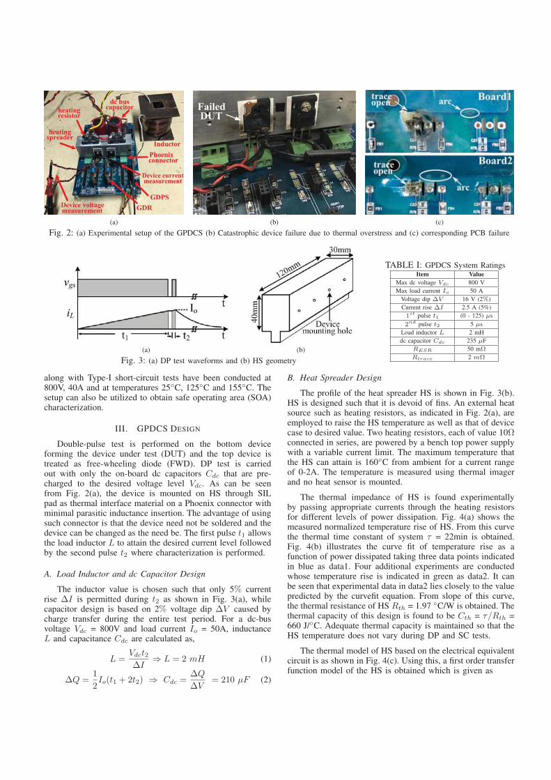
The GPDCS is a half bridge inverter leg mounted on theheat spreader (HS), as shown in Fig. 1. Heating resistors aremounted on the HS that enable setting of the HS temperature tothe desired value prior to the test. The top and bottom devicescomprise of two switches in parallel, which not only facilitatesstudy of parallel IGBT operation, but also enables carrying outType-II short-circuit test under load for fault characterization[12]. TI 28377S based digital controller along with opto-isolated gate drivers (GDR) [13] are employed to drive thedevices. The device current is measured using a RogowskiPEM CWT1 Ultra Mini current probe [14], and device voltagesare measured by passive probes [15] with a twisted wirepair arrangement, as shown in Fig. 2(a). Double-pulse test978-1-5386-9316-2/18/$31.00 c© 2018 IEEE
(a) (b) (c)
Fig. 2: (a) Experimental setup of the GPDCS (b) Catastrophic device failure due to thermal overstress and (c) corresponding PCB failure
(a) (b)
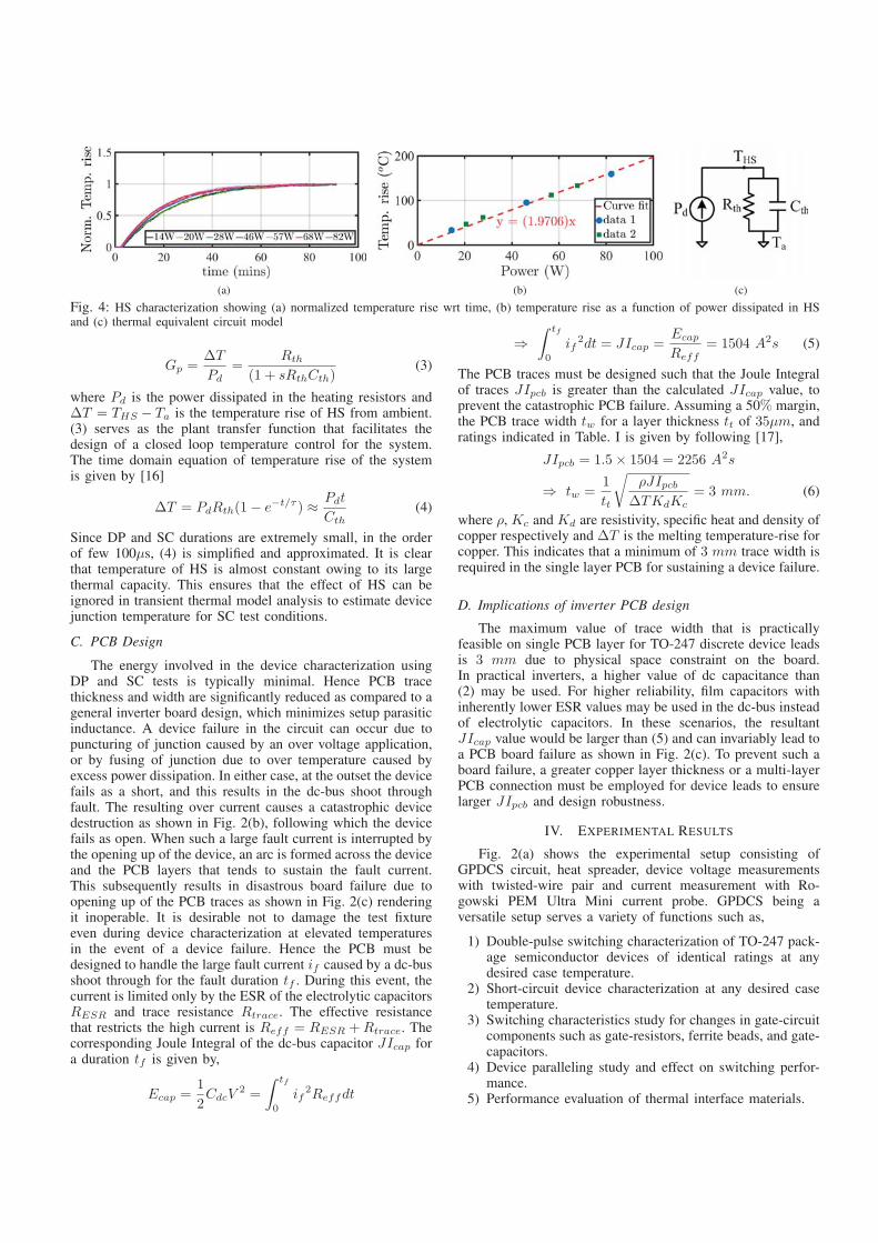
Fig. 3: (a) DP test waveforms and (b) HS geometry
TABLE I: GPDCS System RatingsItem Value
Max dc voltage Vdc 800 VMax load current Io 50 A
Voltage dip ΔV 16 V (2%)Current rise ΔI 2.5 A (5%)1st pulse t1 (0 - 125) μs2nd pulse t2 5 μs
Load inductor L 2 mHdc capacitor Cdc 235 μF
RESR 50 mΩ
Rtrace 2 mΩ
along with Type-I short-circuit tests have been conducted at800V, 40A and at temperatures 25◦C, 125◦C and 155◦C. Thesetup can also be utilized to obtain safe operating area (SOA)characterization.
III. GPDCS DESIGN
Double-pulse test is performed on the bottom deviceforming the device under test (DUT) and the top device istreated as free-wheeling diode (FWD). DP test is carriedout with only the on-board dc capacitors Cdc that are pre-charged to the desired voltage level Vdc. As can be seenfrom Fig. 2(a), the device is mounted on HS through SILpad as thermal interface material on a Phoenix connector withminimal parasitic inductance insertion. The advantage of usingsuch connector is that the device need not be soldered and thedevice can be changed as the need be. The first pulse t1 allowsthe load inductor L to attain the desired current level followedby the second pulse t2 where characterization is performed.
A. Load Inductor and dc Capacitor Design
The inductor value is chosen such that only 5% currentrise ΔI is permitted during t2 as shown in Fig. 3(a), whilecapacitor design is based on 2% voltage dip ΔV caused bycharge transfer during the entire test period. For a dc-busvoltage Vdc = 800V and load current Io = 50A, inductanceL and capacitance Cdc are calculated as,
L =Vdct2ΔI
⇒ L = 2 mH (1)
ΔQ =1
2Io(t1 + 2t2) ⇒ Cdc =
ΔQ
ΔV= 210 μF (2)
B. Heat Spreader Design
The profile of the heat spreader HS is shown in Fig. 3(b).HS is designed such that it is devoid of fins. An external heatsource such as heating resistors, as indicated in Fig. 2(a), areemployed to raise the HS temperature as well as that of devicecase to desired value. Two heating resistors, each of value 10Ωconnected in series, are powered by a bench top power supplywith a variable current limit. The maximum temperature thatthe HS can attain is 160◦C from ambient for a current rangeof 0-2A. The temperature is measured using thermal imagerand no heat sensor is mounted.
The thermal impedance of HS is found experimentallyby passing appropriate currents through the heating resistorsfor different levels of power dissipation. Fig. 4(a) shows themeasured normalized temperature rise of HS. From this curvethe thermal time constant of system τ = 22min is obtained.Fig. 4(b) illustrates the curve fit of temperature rise as afunction of power dissipated taking three data points indicatedin blue as data1. Four additional experiments are conductedwhose temperature rise is indicated in green as data2. It canbe seen that experimental data in data2 lies closely to the valuepredicted by the curvefit equation. From slope of this curve,the thermal resistance of HS Rth = 1.97 ◦C/W is obtained. Thethermal capacity of this design is found to be Cth = τ/Rth =660 J/◦C. Adequate thermal capacity is maintained so that theHS temperature does not vary during DP and SC tests.
The thermal model of HS based on the electrical equivalentcircuit is as shown in Fig. 4(c). Using this, a first order transferfunction model of the HS is obtained which is given as
(a) (b) (c)
Fig. 4: HS characterization showing (a) normalized temperature rise wrt time, (b) temperature rise as a function of power dissipated in HSand (c) thermal equivalent circuit model
Gp =ΔT
Pd=
Rth
(1 + sRthCth)(3)
where Pd is the power dissipated in the heating resistors andΔT = THS − Ta is the temperature rise of HS from ambient.(3) serves as the plant transfer function that facilitates thedesign of a closed loop temperature control for the system.The time domain equation of temperature rise of the systemis given by [16]
ΔT = PdRth(1− e−t/τ ) ≈ Pdt
Cth(4)
Since DP and SC durations are extremely small, in the orderof few 100μs, (4) is simplified and approximated. It is clearthat temperature of HS is almost constant owing to its largethermal capacity. This ensures that the effect of HS can beignored in transient thermal model analysis to estimate devicejunction temperature for SC test conditions.
C. PCB Design
The energy involved in the device characterization usingDP and SC tests is typically minimal. Hence PCB tracethickness and width are significantly reduced as compared to ageneral inverter board design, which minimizes setup parasiticinductance. A device failure in the circuit can occur due topuncturing of junction caused by an over voltage application,or by fusing of junction due to over temperature caused byexcess power dissipation. In either case, at the outset the devicefails as a short, and this results in the dc-bus shoot throughfault. The resulting over current causes a catastrophic devicedestruction as shown in Fig. 2(b), following which the devicefails as open. When such a large fault current is interrupted bythe opening up of the device, an arc is formed across the deviceand the PCB layers that tends to sustain the fault current.This subsequently results in disastrous board failure due toopening up of the PCB traces as shown in Fig. 2(c) renderingit inoperable. It is desirable not to damage the test fixtureeven during device characterization at elevated temperaturesin the event of a device failure. Hence the PCB must bedesigned to handle the large fault current if caused by a dc-busshoot through for the fault duration tf . During this event, thecurrent is limited only by the ESR of the electrolytic capacitorsRESR and trace resistance Rtrace. The effective resistancethat restricts the high current is Reff = RESR +Rtrace. Thecorresponding Joule Integral of the dc-bus capacitor JIcap fora duration tf is given by,
Ecap =1
2CdcV
2 =
∫ tf
0
if2Reffdt
⇒∫ tf
0
if2dt = JIcap =
Ecap
Reff= 1504 A2s (5)
The PCB traces must be designed such that the Joule Integralof traces JIpcb is greater than the calculated JIcap value, toprevent the catastrophic PCB failure. Assuming a 50% margin,the PCB trace width tw for a layer thickness tt of 35μm, andratings indicated in Table. I is given by following [17],
JIpcb = 1.5× 1504 = 2256 A2s
⇒ tw =1
tt
√ρJIpcb
ΔTKdKc= 3 mm. (6)
where ρ, Kc and Kd are resistivity, specific heat and density ofcopper respectively and ΔT is the melting temperature-rise forcopper. This indicates that a minimum of 3 mm trace width isrequired in the single layer PCB for sustaining a device failure.
D. Implications of inverter PCB design
The maximum value of trace width that is practicallyfeasible on single PCB layer for TO-247 discrete device leadsis 3 mm due to physical space constraint on the board.In practical inverters, a higher value of dc capacitance than(2) may be used. For higher reliability, film capacitors withinherently lower ESR values may be used in the dc-bus insteadof electrolytic capacitors. In these scenarios, the resultantJIcap value would be larger than (5) and can invariably lead toa PCB board failure as shown in Fig. 2(c). To prevent such aboard failure, a greater copper layer thickness or a multi-layerPCB connection must be employed for device leads to ensurelarger JIpcb and design robustness.
IV. EXPERIMENTAL RESULTS
Fig. 2(a) shows the experimental setup consisting ofGPDCS circuit, heat spreader, device voltage measurementswith twisted-wire pair and current measurement with Ro-gowski PEM Ultra Mini current probe. GPDCS being aversatile setup serves a variety of functions such as,
1) Double-pulse switching characterization of TO-247 pack-age semiconductor devices of identical ratings at anydesired case temperature.
2) Short-circuit device characterization at any desired casetemperature.
3) Switching characteristics study for changes in gate-circuitcomponents such as gate-resistors, ferrite beads, and gate-capacitors.
4) Device paralleling study and effect on switching perfor-mance.
5) Performance evaluation of thermal interface materials.

-1 0 1 2 3time (μs)
-200
0
200
400
600
800
1000
1200
vce
(V)
-40
-20
0
20
40
60
80
100
vge(V
)
vge vce,25C vce,125C vce,155C
vge
vce
(a)
-1 0 1 2 3time (μs)
-30-15
01530456075
i c(A
)
-40-20020406080100
vge(V
)
vgeic,25Cic,125Cic,155C
vge
ic
(b)
-1 0 1 2 3time (μs)
-200
0
200
400
600
800
1000
1200
vce
(V)
-40
-20
0
20
40
60
80
100
vge(V
)
vge vce,25C vce,125C vce,155C
vce
vge
(c)
-1 0 1 2 3time (μs)
-30-15
01530456075
i c(A
)-40-20020406080100
vge(V
)
vgeic,25Cic,125Cic,155C
ic
vge
(d)
-1 0 1 2 3time (μs)
-2000
200400600800
10001200
vce
(V)
-40-20020406080100
vge(V
)
vge vce,25C vce,125C vce,155C
vcevge
(e)
-1 0 1 2 3time (μs)
-30-15
01530456075
i c(A
)
-40-20020406080100
vge(V
)
vgeic,25Cic,125Cic,155C
ic
vge
(f)
-1 0 1 2 3time (μs)
-200
0
200
400
600
800
1000
1200
vce
(V)
-40
-20
0
20
40
60
80
100
vge(V
)
vge vce,25C vce,125C vce,155C
vge
vce
(g)
-1 0 1 2 3time (μs)
-30-15
01530456075
i c(A
)
-40-20020406080100
vge(V
)
vgeic,25Cic,125Cic,155C
vge
ic
(h)
Fig. 5: Turn-on characteristics of Si IGBTs from different manufacturers and their deviations at elevated temperatures upto 155◦Cat the case showing (a),(b) vce, ic of Si-T1 (c),(d) vce, ic of Si-T2 (e),(f) vce, ic of Si-T3 (g),(h) vce, ic of Si-T4.
A. Double Pulse test on Si devices
Si IGBTs of identical rating of 1200V, 40A namely Si-T1, Si-T2, Si-T3 and Si-T4 are studied. These devices are ofdistinct device technologies such as Field Stop Trench, 3rd GenTrench Stop and from different manufacturers like Infineon,Toshiba, Rohm, Fairchild, STMicroelectronics, IXYS, Cree, ONSemiconductor.
In typical inverter applications, the top and bottom switchesof inverter leg are packaged with the same device. Hence,comparison of the device performance with its default co-packdiode as FWD is crucial. Fig. 5 shows the turn-on and turn-
off characteristics of Si device voltage and current at 25◦C,125◦C and 155◦C during t2 of the DP test. It can be seenthat, all devices exhibit current overshoot during turn-on, dueto reverse recovery charge Qrr of FWD. But, Si-T1 exhibitslowest current overshoot and has minimal deviation in behaviorwith temperature variation as compared to other devices.
The corresponding measured values of Qrr and its devia-tion for the four Si devices are tabulated in Table.II. It can beobserved that, percentage increase in Qrr charge is minimumin Si-T4 and is comparable with Si-T1. It can be observed thatthe total Qrr change is 0.6-2.6 times from 25◦C and 125◦C.
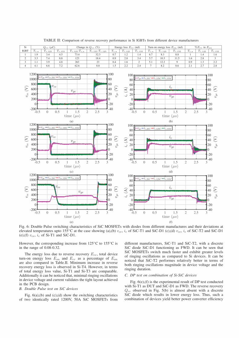
TABLE II: Comparison of reverse recovery performance in Si IGBTs from different device manufacturers
SiIGBT
Qrr (μC) Change in Qrr (%) Energy loss Err (mJ) Turn-on energy loss Eon (mJ) %Err in Eon
Tc,a Tc,125 Tc,155 Tc,125-Tc,a Tc,155-Tc,125 Tc,a Tc,125 Tc,155 Tc,a Tc,125 Tc,155 Tc,a Tc,125 Tc,155
1 1.9 3.4 4.5 73.4 32.3 0.7 1.2 1.4 6.7 8.3 8.8 1 1.4 1.62 3.3 7.4 8.8 123 18.4 0.9 2.8 3.4 5.7 10.3 11.5 1.6 2.8 33 1.1 3.9 4.8 263 23 0.4 1.6 2 5.1 12.2 9 0.9 1.3 2.24 4.1 6.6 7.2 62.6 8.8 1.5 2.2 2.4 7 8.2 8.6 2.1 2.7 2.8
-0.5 0 0.5 1 1.5 2 2.5 3time (μs)
-200
0
200
400
600
800
1000
1200
vce
(V)
-40
-20
0
20
40
60
80
100
vge(V
)
vge vce,25C vce,125C vce,155C
vge
vce
(a)
-0.5 0 0.5 1 1.5 2 2.5 3time (μs)
-40-20
020406080
100
i c(A
)
-40-20020406080100
vge(V
)
vge ic,25C ic,125C ic,155C
vge
ic
(b)
-0.5 0 0.5 1 1.5 2 2.5 3time (μs)
-200
0
200
400
600
800
1000
1200
vce
(V)
-40
-20
0
20
40
60
80
100
vge(V
)
vge vce,25C vce,125C vce,155C
vge
vce
(c)
-0.5 0 0.5 1 1.5 2 2.5 3time (μs)
-40-20
020406080
100i c
(A)
-40-20020406080100
vge(V
)
vge ic,25C ic,125C ic,155C
vge
ic
(d)
-0.5 0 0.5 1 1.5 2 2.5 3time (μs)
-200
0
200
400
600
800
1000
1200
vce
(V)
-40
-20
0
20
40
60
80
100
vge(V
)
vge vce,25C vce,125C vce,155C
vcevge
(e)
-0.5 0 0.5 1 1.5 2 2.5 3time (μs)
-40-20
020406080
100
i c(A
)
-40-20020406080100
vge(V
)
vge ic,25C ic,125C ic,155C
ic
vge
(f)
Fig. 6: Double Pulse switching characteristics of SiC MOSFETs with diodes from different manufactures and their deviations atelevated temperatures upto 155◦C at the case showing (a),(b) vce, ic of SiC-T1 and SiC-D1 (c),(d) vce, ic of SiC-T2 and SiC-D1(e),(f) vce, ic of Si-T1 and SiC-D1.
However, the corresponding increase from 125◦C to 155◦C isin the range of 0.08-0.32.
The energy loss due to reverse recovery Err, total deviceturn-on energy loss Eon and Err as a percentage of Eon
are also compared in Table.II. Minimum increase in reverserecovery energy loss is observed in Si-T4. However, in termsof total energy loss value, Si-T1 and Si-T3 are comparable.Additionally it can be noticed that, minimal ringing oscillationsin device voltage and current validates the tight layout achievedin the PCB design.B. Double Pulse test on SiC devices
Fig. 6(a),(b) and (c),(d) show the switching characteristicsof two identically rated 1200V, 50A SiC MOSFETs from
different manufacturers, SiC-T1 and SiC-T2, with a discreteSiC diode SiC-D1 functioning as FWD. It can be seen thatSiC MOSFETs switch much faster and exhibit greater levelsof ringing oscillations as compared to Si devices. It can benoticed that SiC-T2 performes relatively better in terms ofboth ringing oscillations magnitude in device voltage and theringing duration.
C. DP test on combination of Si-SiC devices
Fig. 6(e),(f) is the experimental result of DP test conductedwith Si-T1 as DUT and SiC-D1 as FWD. The reverse recoveryQrr observed in Fig. 5(b) is almost absent with a discreteSiC diode which results in lower energy loss. Thus, such acombination of devices yield better power converter efficiency
-5 0 5 10time (μs)
-200
-100
0
100
200
i c(A
)
-20
0
20
40
60
vge(V
)
vgeic,25Cic,125Cic,155C
vge
ic
(a)
-5 0 5 10time (μs)
-300-200-100
0100200300400
i c(A
)
-20-1001020304050
vge(V
)
vgeic,25Cic,125C
vge
ic
(b)
Fig. 7: Type-I short-circuit characteristics and its deviation at elevated temperatures showing (a) Si-T1 (b) Si-T2 devices.
in high frequency hard switched DC-DC applications.
D. Type-I short circuit test on Si devices
In terms of short circut performance, while Si-T1 andSi-T2 are rated for 10μs short circuit withstand capability,Si-T3 and Si-T4 are rated for only 5μs. Hence, Type-I SCexperiment is conducted only on Si-T1 and Si-T2 at elevatedtemperatures as shown in Fig. 7. It can be observed that theshort circuit current value decreases at elevated temperatures.This is due to the reduction of transconductance gm of thedevice at higher temperatures [18]. It can be seen in Fig. 7(a)that Si-T1 sustains SC for 8μs even when the case temperatureis at 155◦C while Si-T2 is unable to withstand SC currentand results in a catastrophic thermal failure such as the caseshown in Fig. 2(b). SOA characteristics of the device can beobtained by plotting ic with respect to vce. Such a fault studyat elevated temperature is helpful in comparing the robustnessof semiconductor devices at extreme operating conditions.
V. CONCLUSION
This paper presents the design of a PCB based generalpurpose discrete device characterization setup, using whichTO-247 package switches can be studied with double pulseand short-circuit tests at desired operating case temperature.The thermal design of the HS and its characterization methodto facilitate elevated temperature tests are explained. The setupcan be used to test devices upto an elevated temperature of160◦C. A failure mode of the power PCB of general pur-pose device characterization setup during elevated temperaturetests is presented. The necessary PCB design change to beincorporated to prevent board failures during such tests areoutlined. Similar rated Si and SiC device characteristics ofdifferent device technologies from various manufacturers arecompared experimentally at elevated temperatures, from whichreverse recovery charge and the corresponding losses incurredin device are obtained. These tests also bring out the significantvariations in ruggedness of the different devices from differentmanufacturers. Also, same board can be used for differentdevices. Tests conducted on different combination of powerdevices verify the performance of the setup and also aidin making appropriate choice for a given power conversionapplication.
REFERENCES
[1] L. Umanand, Power electronics essentials and applications. New Delhi,India: Wiley Publishers, 2009.
[2] S. S. Ahmad and G. Narayanan, “Double pulse test based switchingcharacterization of SiC MOSFET,” in Nat. Power Electron. Conf.(NPEC), pp. 319–324, Dec 2017.
[3] P. Ganesan, R. Manju, K. R. Razila, and R. J. Vijayan, “Characterisationof 1200V, 35A SiC Mosfet using double pulse circuit,” in IEEE Int.Conf. on Power Electron. Drives and Energy Syst. (PEDES), pp. 1–6,Dec 2016.
[4] H. Li and S. Munk-Nielsen, “Detail study of SiC MOSFET switchingcharacteristics,” in 2014 IEEE 5th Int. Symp. on Power Electron. forDistrib. Generation Syst. (PEDG), pp. 1–5, June 2014.
[5] S. Musumeci, R. Pagano, A. Raciti, F. Frisina, and M. Melito, “Transientbehavior of IGBTs submitted to fault under load conditions,” in IEEEInd. Appl. Conf. 37th IAS Annu. Meeting, vol. 3, pp. 2182–2189, Oct2002.
[6] S. Hazra, S. Madhusoodhanan, G. K. Moghaddam, K. Hatua, andS. Bhattacharya, “Design Considerations and Performance Evaluationof 1200-V 100-A SiC MOSFET-Based Two-Level Voltage SourceConverter,” IEEE Trans. on Ind. Appl., vol. 52, pp. 4257–4268, Sept2016.
[7] R. S. Chokhawala, J. Catt, and L. Kiraly, “A discussion on IGBT short-circuit behavior and fault protection schemes,” IEEE Trans. on Ind.Appl., vol. 31, pp. 256–263, March 1995.
[8] M. Rahimo, F. Canales, R. A. Minamisawa, C. Papadopoulos, U. Vem-ulapati, A. Mihaila, S. Kicin, and U. Drofenik, “Characterization ofa Silicon IGBT and Silicon Carbide MOSFET Cross-Switch Hybrid,”IEEE Trans. on Power Electron., vol. 30, pp. 4638–4642, Sept 2015.
[9] H. Qin, D. Wang, Y. Zhang, D. Fu, and C. Zhao, “The characteristic andswitching strategies of SiC MOSFET assisted Si IGBT hybrid switch,”in Proc. Annu. Conf. IEEE Ind. Electron. Soc. (IECON), pp. 1604–1609,Oct 2017.
[10] P. Vaculik, “The properties of SiC in comparison with Si semiconductordevices,” in 2013 Int. Conf. on Appl. Electron., pp. 1–4, Sept 2013.
[11] T. Daranagama, F. Udrea, T. Logan, and R. McMahon, “A performancecomparison of SiC and Si devices in a bi-directional converter fordistributed energy storage systems,” in IEEE 7th Int. Symp. on PowerElectron. for Distrib. Generation Syst. (PEDG), pp. 1–8, June 2016.
[12] “IGBT Basic II.” Application Note, On Semiconductor, Apr 2002.[13] A. K. Adapa, D. Venkatramanan, and V. John, “Auxiliary subsystems of
a General-Purpose IGBT Stack for high-performance laboratory powerconverters,” Sadhana, vol. 42, pp. 1355–1362, Aug 2017.
[14] “Datasheet of CWT Ultra Mini,” Available at http://www.pem.com, lastaccessed on Jul 2017.
[15] “Datasheet of Tektronix probe,” Available at http://www.tek.com, lastaccessed on Aug 2017.
[16] “Transient Thermal Measurements and thermal equivalent circuit mod-els.” Application Note, Infineon Technologies, Dec 2015.
[17] “IPC-2221A Generic standard on printed board design,” May 2003.[18] V. Bolloju and J. Yang, “Influence of short circuit conditions on IGBT
short circuit current in motor drives,” in 2011 Twenty-Sixth Annu. IEEEAppl. Power Electron. Conf. and Expo. (APEC), pp. 1675–1679, March2011.


![organic compounds - eprints.iisc.ac.ineprints.iisc.ac.in/21013/1/1full_text.pdf · 1-(2,4-Dichlorophenyl)-3-[4-(dimethyl-amino)phenyl]prop-2-enone Navin N. Bappalige,a Brinda,b* Y](https://img.pdfslide.net/doc/110x75/5f8f7571a5d0693815000c73/organic-compounds-1-24-dichlorophenyl-3-4-dimethyl-aminophenylprop-2-enone.jpg)