Embed Size (px)
DESCRIPTION
Design and Performance of the 6 GS/s Waveform Digitizing Chip DRS4. at 40 mW per channel. Stefan Ritt Paul Scherrer Institute, Switzerland. Switched Capacitor Array. Cons No continuous acquisition No precise timing External (commercial) ADC needed Pros - PowerPoint PPT Presentation
Citation preview
Design and Performance of the 6 GS/s Waveform Digitizing Chip
DRS4
Stefan RittPaul Scherrer Institute, Switzerland
at 40 mW per channel
Oct. 21st, 2008 IEEE/NSS Dresden 2
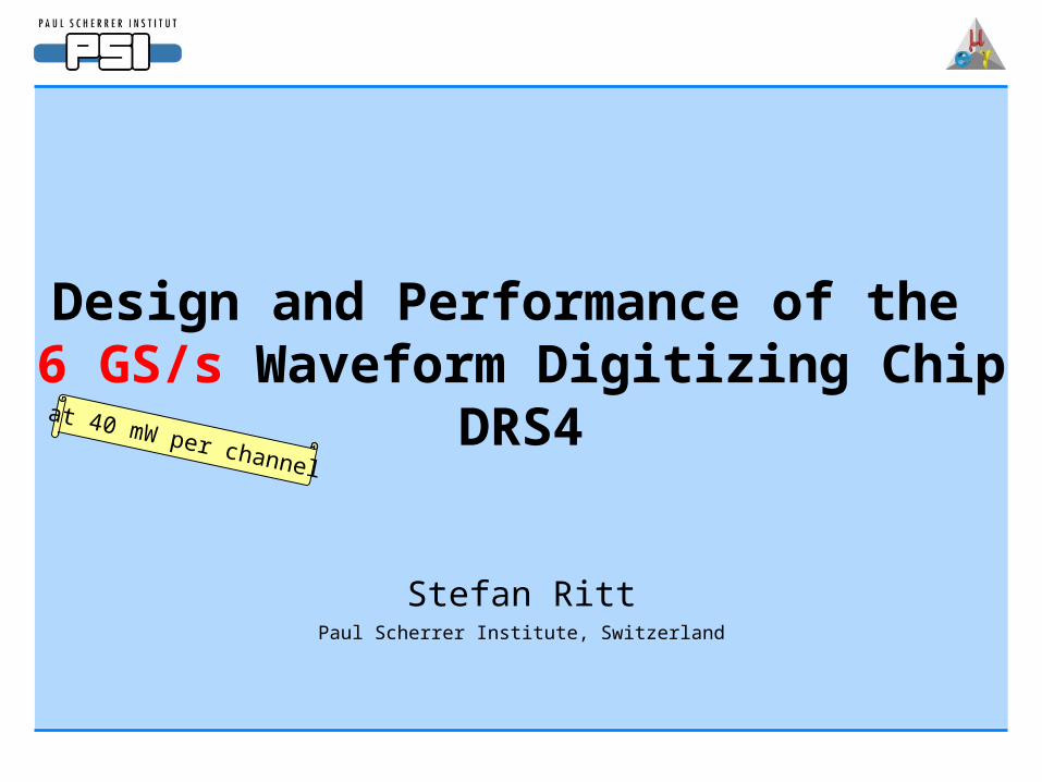
Switched Capacitor Array
•Cons
• No continuous acquisition
• No precise timing
• External (commercial) ADC needed
•Pros
• High speed (6 GHz) high resolution (11.5 bit resol.)
• High channel density (9 channels on 5x5 mm2)
• Low power (10-40 mW / channel)
• Low cost (~ 10$ / channel)
t t t t t
Oct. 21st, 2008 IEEE/NSS Dresden 3
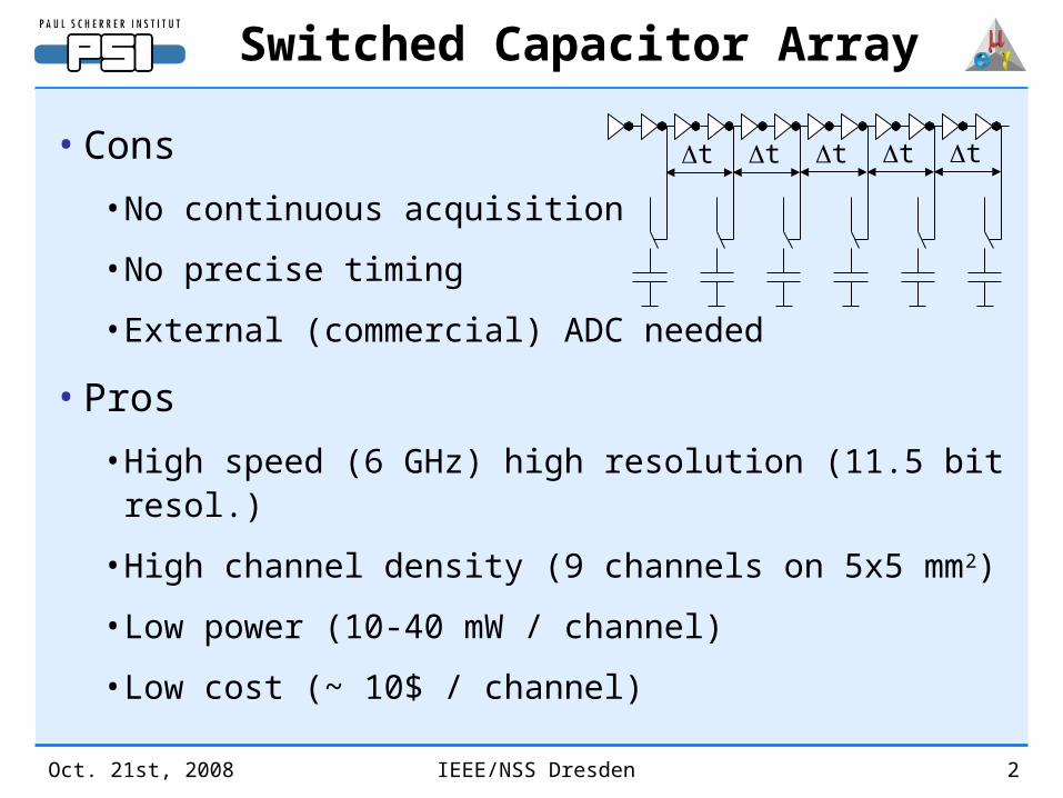
DRS4
• Fabricated in 0.25 m 1P5M MMC process(UMC), 5 x 5 mm2, radiation hard
• 8+1 ch. each 1024 cells
• Differential inputs,differential outputs
• Sampling speed 500 MHz … 6 GHz,PLL stabilized
• Readout speed 30 MHz, multiplexedor in parallel
IN0
IN1
IN2
IN3
IN4
IN5
IN6
IN7
IN8
STOP SHIFT REGISTER
READ SHIFT REGISTER
WSROUT
CONFIG REGISTER
RSRLOAD
DENABLE
WSRIN
DWRITE
DSPEED PLLOUT
DOMINO WAVE CIRCUIT
PLL
AGND
DGND
AVDD
DVDD
DTAPREFCLKPLLLCK A0 A1 A2 A3
EN
AB
LE
OUT0
OUT1
OUT2
OUT3
OUT4
OUT5
OUT6
OUT7
OUT8/MUXOUT
BIASO-OFS
ROFSSROUT
RESETSRCLK
SRIN
F U N C T IO N A L B L O C K D IA G R A M
MUX
WR
ITE
SH
IFT
RE
GIS
TE
R
WR
ITE
CO
NF
IG R
EG
IST
ER
CHANNEL 0
CHANNEL 1
CHANNEL 2
CHANNEL 3
CHANNEL 4
CHANNEL 5
CHANNEL 6
CHANNEL 7
CHANNEL 8
MUX
LVDS
Oct. 21st, 2008 IEEE/NSS Dresden 4
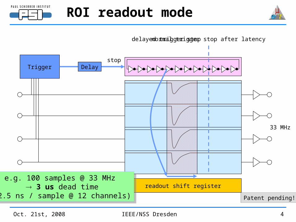
ROI readout mode
readout shift register
Triggerstop
normal trigger stop after latency
Delay
delayed trigger stop
Patent pending!
33 MHz
e.g. 100 samples @ 33 MHz 3 us dead time
(2.5 ns / sample @ 12 channels)
e.g. 100 samples @ 33 MHz 3 us dead time
(2.5 ns / sample @ 12 channels)
Oct. 21st, 2008 IEEE/NSS Dresden 5
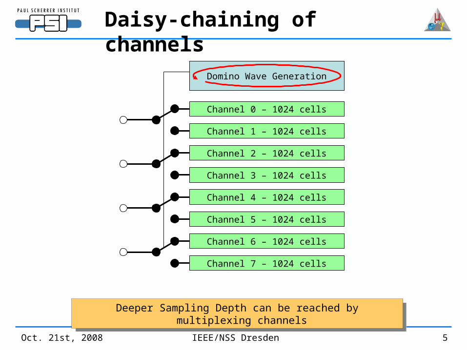
Daisy-chaining of channels
Channel 0 – 1024 cells
Channel 1 – 1024 cells
Channel 2 – 1024 cells
Channel 3 – 1024 cells
Channel 4 – 1024 cells
Channel 5 – 1024 cells
Channel 6 – 1024 cells
Channel 7 – 1024 cells
Domino Wave Generation
Deeper Sampling Depth can be reached by multiplexing channels
Deeper Sampling Depth can be reached by multiplexing channels
Oct. 21st, 2008 IEEE/NSS Dresden 6
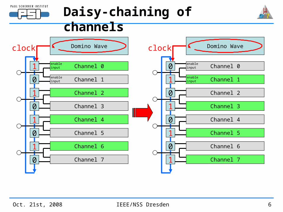
Daisy-chaining of channels
Channel 0
Channel 1
Channel 2
Channel 3
Channel 4
Channel 5
Channel 6
Channel 7
Domino Wave
1
clock
0
1
0
1
0
1
0
enableinput
enableinput
Channel 0
Channel 1
Channel 2
Channel 3
Channel 4
Channel 5
Channel 6
Channel 7
Domino Wave
1
clock
0
1
0
1
0
1
0
enableinput
enableinput
Oct. 21st, 2008 IEEE/NSS Dresden 7
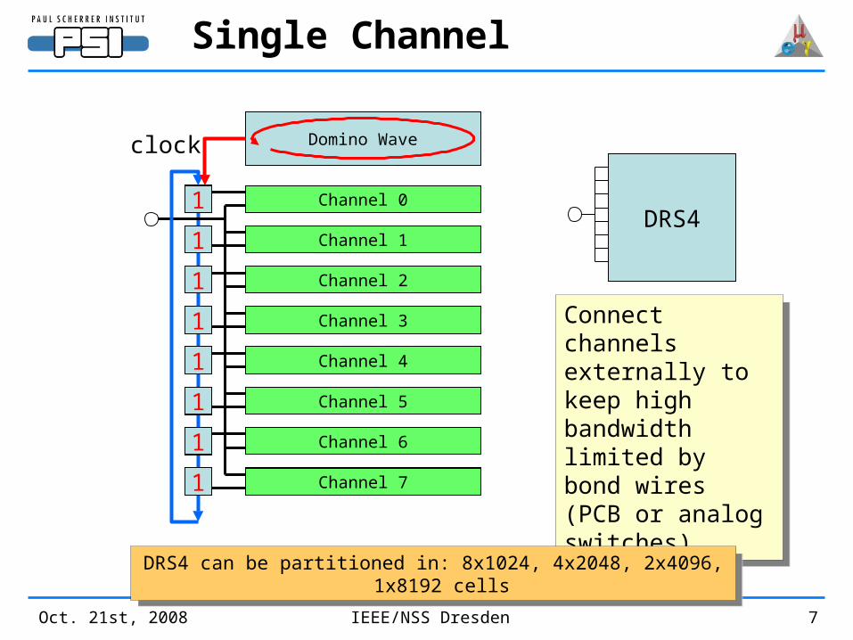
Single Channel
Channel 0
Channel 1
Channel 2
Channel 3
Channel 4
Channel 5
Channel 6
Channel 7
Domino Wave
0
clock
0
0
0
0
0
0
0
1 Channel 0
Channel 11
Channel 21
Channel 31
Channel 41
Channel 51
Channel 61
Channel 71
DRS4
Connect channels externally to keep high bandwidth limited by bond wires (PCB or analog switches)
Connect channels externally to keep high bandwidth limited by bond wires (PCB or analog switches)
DRS4 can be partitioned in: 8x1024, 4x2048, 2x4096, 1x8192 cells
DRS4 can be partitioned in: 8x1024, 4x2048, 2x4096, 1x8192 cells
Oct. 21st, 2008 IEEE/NSS Dresden 8
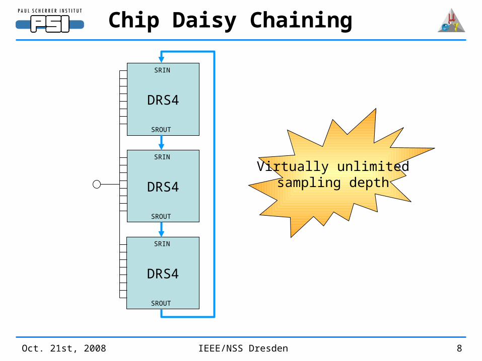
Chip Daisy Chaining
DRS4
SROUT
SRIN
DRS4
SROUT
SRIN
DRS4
SROUT
SRIN
Virtually unlimitedsampling depth
Oct. 21st, 2008 IEEE/NSS Dresden 9
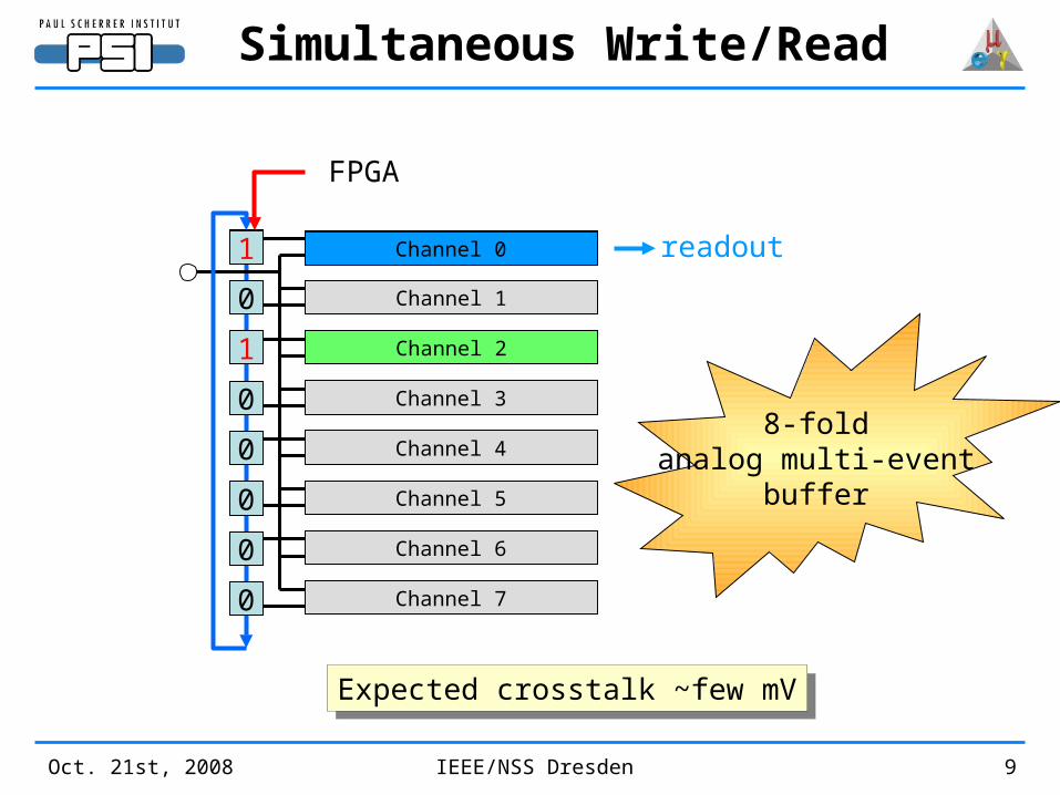
Simultaneous Write/Read
Channel 0
Channel 1
Channel 2
Channel 3
Channel 4
Channel 5
Channel 6
Channel 7
0
FPGA
0
0
0
0
0
0
0
1 Channel 0
Channel 11
Channel 0 readout
8-foldanalog multi-event
buffer
Channel 21
Channel 10
Expected crosstalk ~few mVExpected crosstalk ~few mV
Oct. 21st, 2008 IEEE/NSS Dresden 10
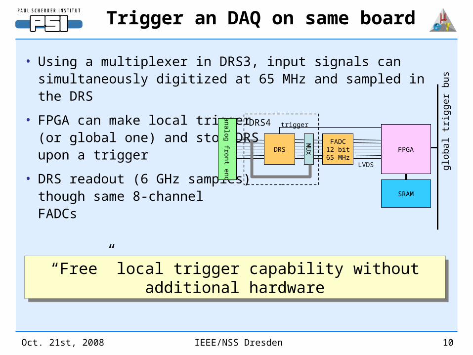
Trigger an DAQ on same board
• Using a multiplexer in DRS3, input signals can simultaneously digitized at 65 MHz and sampled in the DRS
• FPGA can make local trigger(or global one) and stop DRSupon a trigger
• DRS readout (6 GHz samples)though same 8-channel FADCs
an
alo
g fro
nt e
nd
DRSFADC12 bit
65 MHzM
UX FPGA
trigger
LVDS
SRAM
DRS4
glo
bal tr
igger
bu
s
“Free” local trigger capability without additional hardware
“Free” local trigger capability without additional hardware
DRS4
Test Results
Oct. 21st, 2008 IEEE/NSS Dresden 12
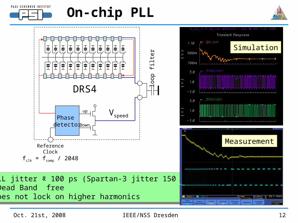
On-chip PLL
ReferenceClock
fclk = fsamp / 2048
Vspeed
• PLL jitter « 100 ps (Spartan-3 jitter 150 ps)• “Dead Band” free• Does not lock on higher harmonics
• PLL jitter « 100 ps (Spartan-3 jitter 150 ps)• “Dead Band” free• Does not lock on higher harmonics
loop
filt
er
DRS4
Simulation
Measurement
Phase detector
up
down
Oct. 21st, 2008 IEEE/NSS Dresden 13
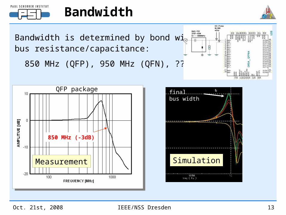
Bandwidth
Bandwidth is determined by bond wire and internalbus resistance/capacitance:
850 MHz (QFP), 950 MHz (QFN), ??? (flip-chip)
850 MHz (-3dB)
QFP package finalbus width
SimulationMeasurement
Oct. 21st, 2008 IEEE/NSS Dresden 14
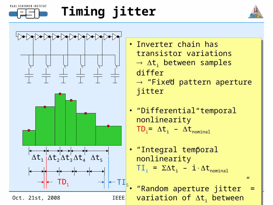
Timing jitter
t1 t2 t3 t4 t5
• Inverter chain has transistor variations ti between samples differ “Fixed pattern aperture jitter”
• “Differential temporal nonlinearity” TDi= ti – tnominal
• “Integral temporal nonlinearity”TIi = ti – itnominal
• “Random aperture jitter” = variation of ti between measurements
• Inverter chain has transistor variations ti between samples differ “Fixed pattern aperture jitter”
• “Differential temporal nonlinearity” TDi= ti – tnominal
• “Integral temporal nonlinearity”TIi = ti – itnominal
• “Random aperture jitter” = variation of ti between measurements
TD1 TI5
Oct. 21st, 2008 IEEE/NSS Dresden 15
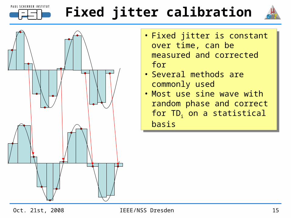
Fixed jitter calibration
• Fixed jitter is constant over time, can be measured and corrected for
• Several methods are commonly used
• Most use sine wave with random phase and correct for TDi on a statistical basis
• Fixed jitter is constant over time, can be measured and corrected for
• Several methods are commonly used
• Most use sine wave with random phase and correct for TDi on a statistical basis
Oct. 21st, 2008 IEEE/NSS Dresden 16
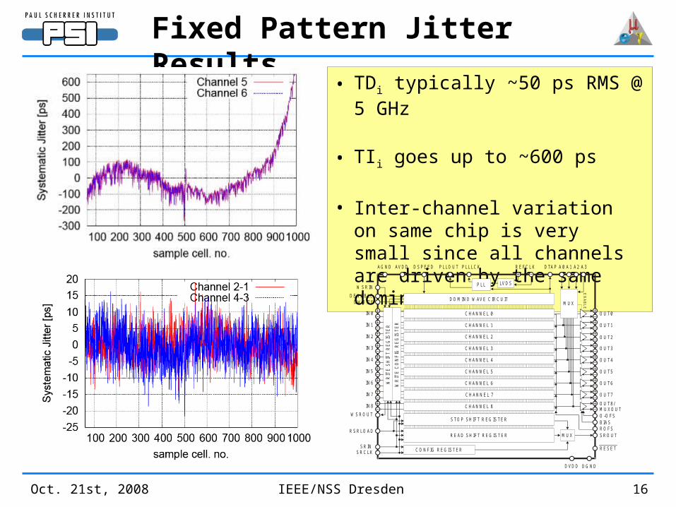
Fixed Pattern Jitter Results
• TDi typically ~50 ps RMS @ 5 GHz
• TIi goes up to ~600 ps
• Inter-channel variation on same chip is very small since all channels are driven by the same domino wave
IN0
IN1
IN2
IN3
IN4
IN5
IN6
IN7
IN8
STOP SHIFT REGISTER
READ SHIFT REGISTER
WSROUT
CONFIG REGISTER
RSRLOAD
DENABLE
WSRIN
DWRITE
DSPEED PLLOUT
DOMINO WAVE CIRCUIT
PLL
AGND
DGND
AVDD
DVDD
DTAPREFCLKPLLLCK A0 A1 A2 A3
EN
AB
LE
OUT0
OUT1
OUT2
OUT3
OUT4
OUT5
OUT6
OUT7
OUT8/MUXOUT
BIASO-OFS
ROFSSROUT
RESETSRCLK
SRIN
F U N C T IO N A L B L O C K D IA G R A M
MUX
WR
ITE
SH
IFT
RE
GIS
TE
R
WR
ITE
CO
NF
IG R
EG
IST
ER
CHANNEL 0
CHANNEL 1
CHANNEL 2
CHANNEL 3
CHANNEL 4
CHANNEL 5
CHANNEL 6
CHANNEL 7
CHANNEL 8
MUX
LVDS
Oct. 21st, 2008 IEEE/NSS Dresden 17
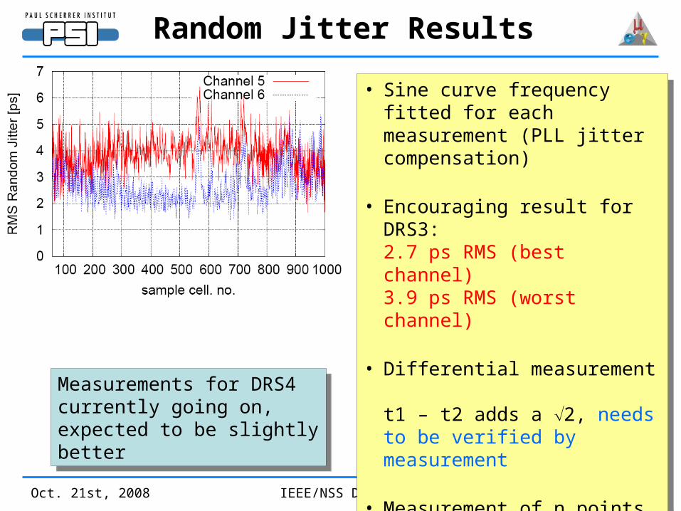
Random Jitter Results
• Sine curve frequency fitted for each measurement (PLL jitter compensation)
• Encouraging result for DRS3:2.7 ps RMS (best channel)3.9 ps RMS (worst channel)
• Differential measurement t1 – t2 adds a 2, needs to be verified by measurement
• Measurement of n points on a rising edge of a signal improves by n
Measurements for DRS4 currently going on, expected to be slightly better
Measurements for DRS4 currently going on, expected to be slightly better
Oct. 21st, 2008 IEEE/NSS Dresden 18
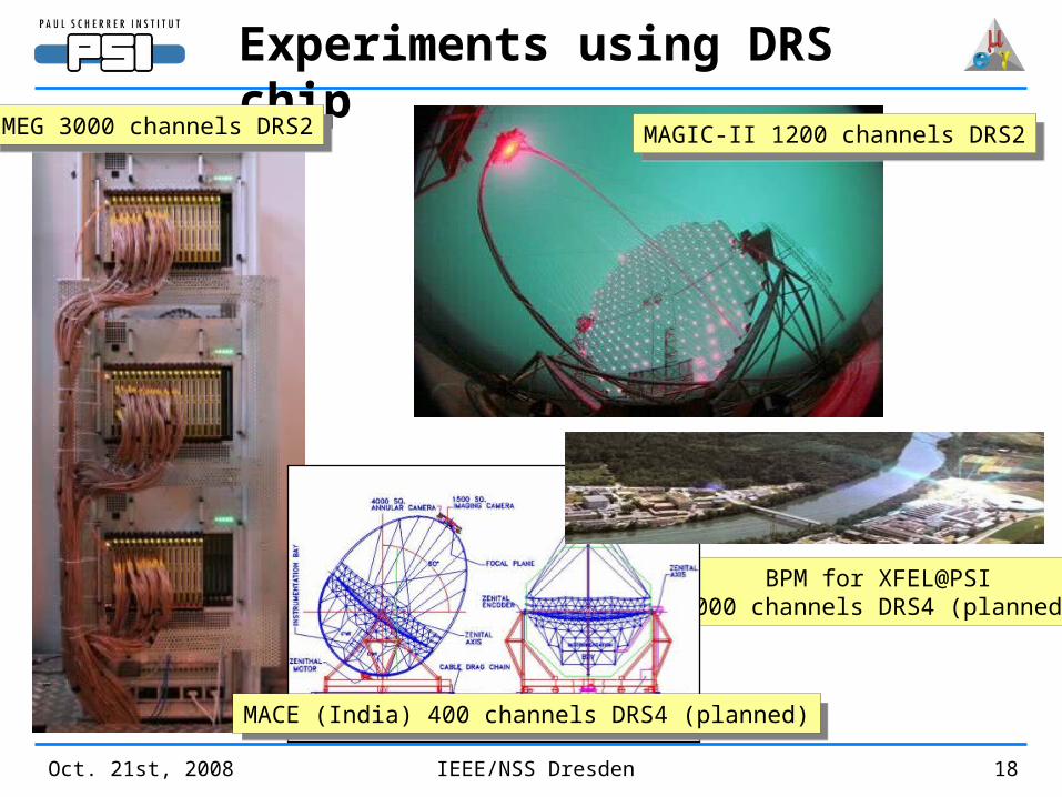
Experiments using DRS chip
MAGIC-II 1200 channels DRS2MAGIC-II 1200 channels DRS2MEG 3000 channels DRS2MEG 3000 channels DRS2
BPM for XFEL@PSI1000 channels DRS4 (planned)
MACE (India) 400 channels DRS4 (planned)MACE (India) 400 channels DRS4 (planned)
Oct. 21st, 2008 IEEE/NSS Dresden 19
Availability
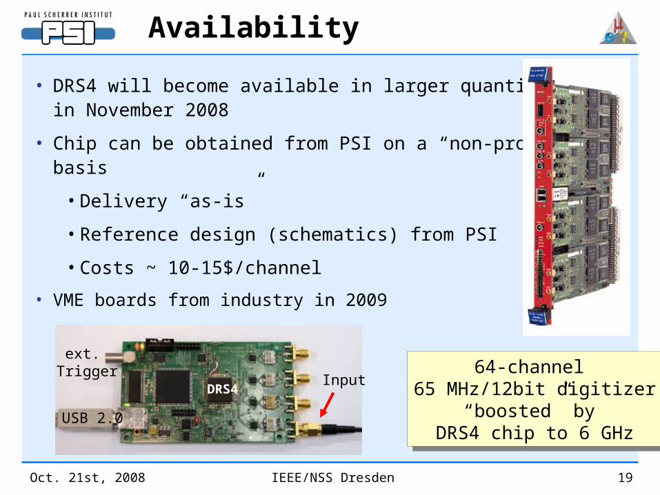
• DRS4 will become available in larger quantities in November 2008
• Chip can be obtained from PSI on a “non-profit” basis
• Delivery “as-is”
• Reference design (schematics) from PSI
• Costs ~ 10-15$/channel
• VME boards from industry in 2009
64-channel 65 MHz/12bit digitizer
“boosted” by DRS4 chip to 6 GHz
64-channel 65 MHz/12bit digitizer
“boosted” by DRS4 chip to 6 GHz
Input
USB 2.0
ext. Trigger
DRS4
Oct. 21st, 2008 IEEE/NSS Dresden 20
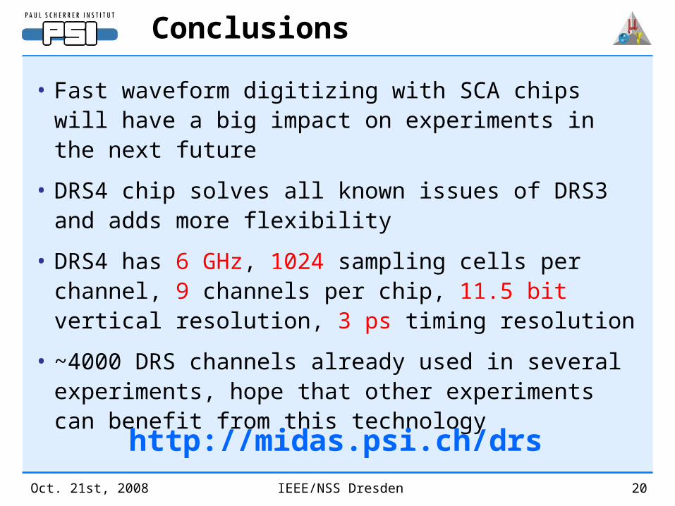
Conclusions
• Fast waveform digitizing with SCA chips will have a big impact on experiments in the next future
• DRS4 chip solves all known issues of DRS3 and adds more flexibility
• DRS4 has 6 GHz, 1024 sampling cells per channel, 9 channels per chip, 11.5 bit vertical resolution, 3 ps timing resolution
• ~4000 DRS channels already used in several experiments, hope that other experiments can benefit from this technology
http://midas.psi.ch/drs

Oct. 21st, 2008 IEEE/NSS Dresden 22
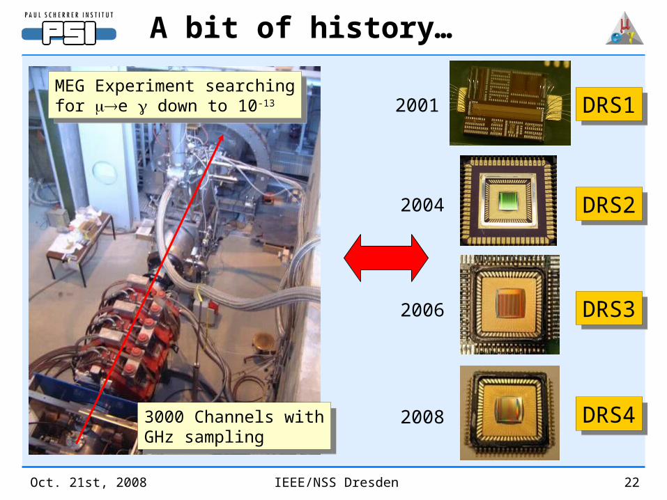
A bit of history…
DRS2DRS2
DRS3DRS3
DRS1DRS1MEG Experiment searchingfor e down to 10-13
MEG Experiment searchingfor e down to 10-13
DRS4DRS42008
2006
2004
2001
3000 Channels withGHz sampling
3000 Channels withGHz sampling
Oct. 21st, 2008 IEEE/NSS Dresden 23
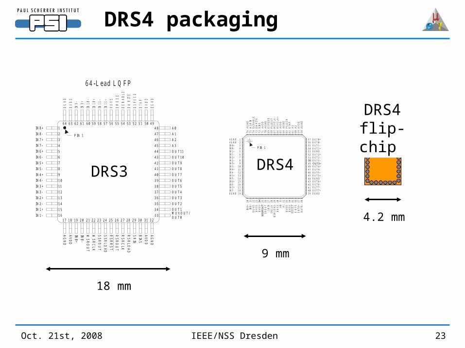
DRS4 packaging
6 4 -L ea d L Q F P
6 4 -L ea d Q F N
17
64
18
63
19
62
20
61
21
60
22
59
23
58
24
57
25
56
26
55
27
54
28
53
29
52
30
51
31
50
32
49
3316
3415
3514
3613
3712
3811
3910
409
418
427
436
445
454
463
472
481
DRS3TOP VIEW
(N ot to Scale)
PIN 1
DR S3TO P VIEW
(Not to Scale)
PIN 1
P IN C O N F IG U R AT IO N
A 0
A 0
IN8+
IN 8+
A 1
A 1
IN8-
IN 8-A 2
A 2
IN7+
IN 7+A 3A 3
IN7-IN 7-OU T11 OU T 11IN6+IN 6+
OU T10 OU T 1 0IN6- IN 6-
OU T9OU T 9
IN5+IN 5+
OU T8OU T 8
IN5-IN 5-
OU T7
OU T 7
IN4+
IN 4+
OU T6
OU T 6
IN4-
IN 4-
OU T5
OU T 5
IN3+
IN 3+
OU T4
OU T 4
IN3-
IN 3-
OU T3
OU T 3
IN2+
IN 2+
OU T2
OU T 2
IN2-
IN 2-
OU T1
OU T 1
IN1+
IN 1+
IN1-
IN 1-
DG
ND
DV
DD
DTA
P
DS
PE
ED
DW
RIT
E
DE
NA
BL
E
DM
OD
E
RO
FS
IN11
+
IN11
-
IN1
0+
IN1
0-
IN9
+
IN9
-
DV
DD
DG
ND
DG
ND
DV
DD
DTA
PD
SP
EE
DD
WR
ITE
DE
NA
BL
ED
MO
DE
RO
FS
IN11
+IN
11-
IN10
+IN
10-
IN9+
IN9-
DV
DD
DG
ND
M UXOUT/OU T0
MU X O UT/OU T 0
AG
ND
AG
ND
AV
DD
AV
DD
BIA
S
BIA
S
SR
IN
SR
IN
RS
RL
OA
D
RS
RL
OA
D
RS
RC
LK
RS
RC
LK
RS
RO
UT
RS
RO
UT
RS
RR
ST
RS
RR
ST
SS
RL
OA
D
SS
RLO
AD
SS
RO
UT
SS
RO
UT
WS
RC
LK
WS
RC
LK
WS
RO
UT
WS
RO
UT
IN0-
IN0-
IN0+
IN0+
AV
DD
AV
DD
AG
ND
AG
ND
DRS3 DRS4
9 mm
18 mm
4.2 mm
DRS4flip-chip PIN 1
O U T 0 +5 7A G N DO U T 0 -5 6A G N D 2
1
O U T 1 -5 5IN 0+ 3O U T 1 +D G N D
D G N D
D G N D
5 4IN 0- 4
O U T 2 +5 3IN 1+ 5
O U T 2 -5 2IN 1- 6
O U T 3 -5 1IN 2+ 7
IN 2- 8
O U T 4 +4 9IN 3+ 9
O U T 4 -4 8IN 3- 1 0
O U T 5 -4 7IN 4+ 11
O U T 5 +4 6IN 4- 1 2
O U T 6 +
4 5IN 5+ 1 3
O U T 6 -
4 4IN 5- 1 4
O U T 7 -
4 3IN 6+ 1 5IN 6-IN 7+IN 7-D G N D
1 61 71 81 9
AG
ND
AG
ND
AV
DD
A2
A3
BIA
S
DT
AP
RE
FC
LK
+R
EF
CL
K-
PL
LLC
K
PL
LOU
TD
SP
EE
D
DW
RIT
ED
EN
AB
LE
WS
RIN
AV
DD
AV
DD
AG
ND
AG
ND
76
75
63
64
65
66
67
68
69
70
71
72
73
74
62
61
60
59
58
O U T 7 +
4 24 14 03 9
OU
T8
-
35 36 37 38O
UT
8+
34
O-O
FS
33D
VD
DD
VD
DR
ES
ET
32
A1
31A
030
RO
FS
29R
SR
LO
AD
28S
RC
LK27
SR
IN26
SR
OU
T25
DV
DD
DV
DD
23D
GN
D2
2IN
8-
21IN
8+
20
Oct. 21st, 2008 IEEE/NSS Dresden 24
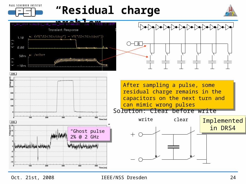
“Residual charge” problem
R
“Ghost pulse”2% @ 2 GHz
“Ghost pulse”2% @ 2 GHz
After sampling a pulse, some residual charge remains in the capacitors on the next turn and can mimic wrong pulses
After sampling a pulse, some residual charge remains in the capacitors on the next turn and can mimic wrong pulsesSolution: Clear before write
write clearImplemented
in DRS4
Implementedin DRS4
Oct. 21st, 2008 IEEE/NSS Dresden 25
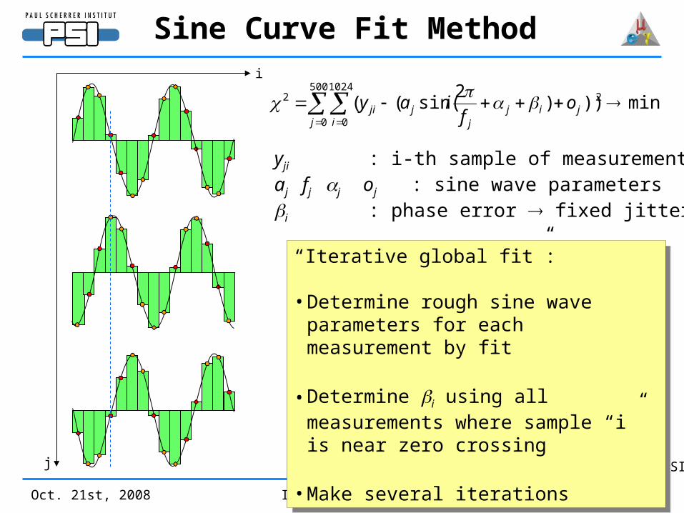
Sine Curve Fit Method
S. Lehner, B. Keil, PSI
i
j
500
0
1024
0
22 min)))2
sin(((j i
jijj
jji of
iay
yji : i-th sample of measurement jaj fj j oj : sine wave parametersi : phase error fixed jitter
“Iterative global fit”:
•Determine rough sine wave parameters for each measurement by fit
•Determine i using all measurements where sample “i” is near zero crossing
•Make several iterations
“Iterative global fit”:
•Determine rough sine wave parameters for each measurement by fit
•Determine i using all measurements where sample “i” is near zero crossing
•Make several iterations
Oct. 21st, 2008 IEEE/NSS Dresden 26
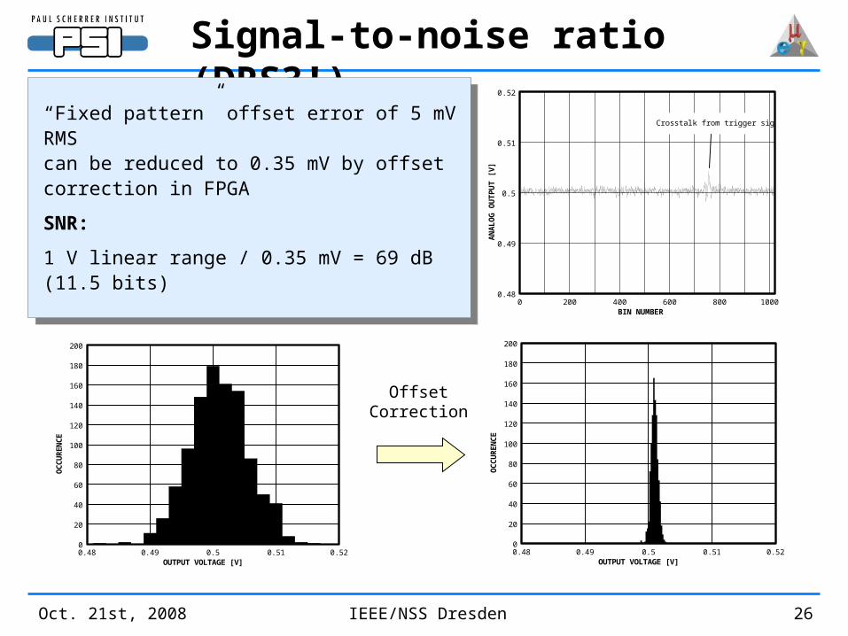
Signal-to-noise ratio (DRS3!)
“Fixed pattern” offset error of 5 mV RMScan be reduced to 0.35 mV by offsetcorrection in FPGA
SNR:
1 V linear range / 0.35 mV = 69 dB (11.5 bits)
“Fixed pattern” offset error of 5 mV RMScan be reduced to 0.35 mV by offsetcorrection in FPGA
SNR:
1 V linear range / 0.35 mV = 69 dB (11.5 bits)
AN
AL
OG
OU
TP
UT
[V
]
BIN NUMBER0 200 400 600 800 1000
0.48
0.49
0.5
0.51
0.52
Crosstalk from trigger signal
OC
CU
RE
NC
E
OUTPUT VOLTAGE [V]0.48 0.49 0.5 0.51 0.520
20
40
60
80
100
120
140
160
180
200
OC
CU
RE
NC
E
OUTPUT VOLTAGE [V]0.48 0.49 0.5 0.51 0.520
20
40
60
80
100
120
140
160
180
200
OffsetCorrection
Oct. 21st, 2008 IEEE/NSS Dresden 27
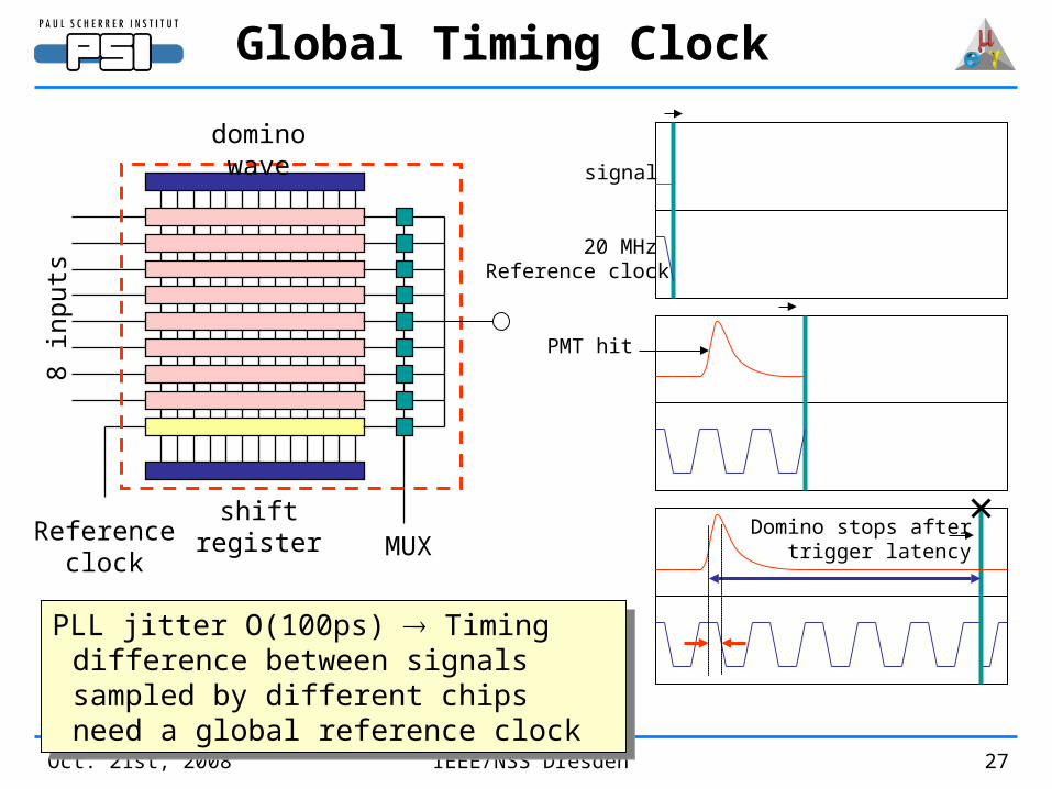
Global Timing Clock
signal
20 MHz Reference clock
PMT hit
Domino stops aftertrigger latency
8 inp
uts
shift registerReference
clock
domino wave
MUX
PLL jitter O(100ps) Timing difference between signals sampled by different chips need a global reference clock
PLL jitter O(100ps) Timing difference between signals sampled by different chips need a global reference clock
Oct. 21st, 2008 IEEE/NSS Dresden 28
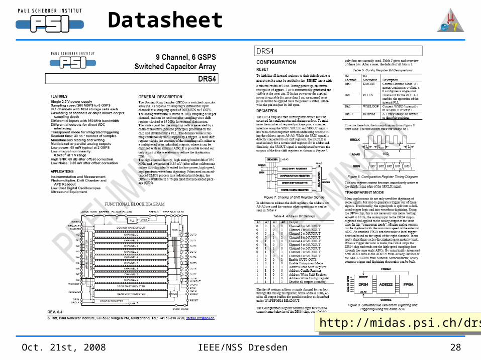
Datasheet
http://midas.psi.ch/drshttp://midas.psi.ch/drs
Oct. 21st, 2008 IEEE/NSS Dresden 29
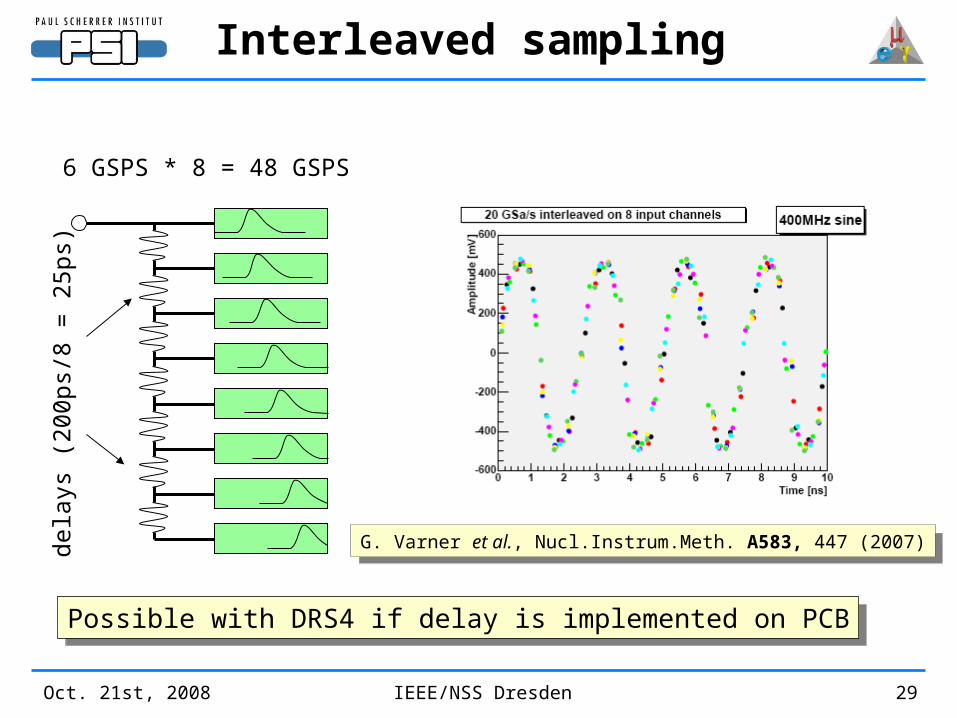
Interleaved samplingdela
ys
(200p
s/8 =
25ps)
G. Varner et al., Nucl.Instrum.Meth. A583, 447 (2007)G. Varner et al., Nucl.Instrum.Meth. A583, 447 (2007)
6 GSPS * 8 = 48 GSPS
Possible with DRS4 if delay is implemented on PCBPossible with DRS4 if delay is implemented on PCB
Oct. 21st, 2008 IEEE/NSS Dresden 30
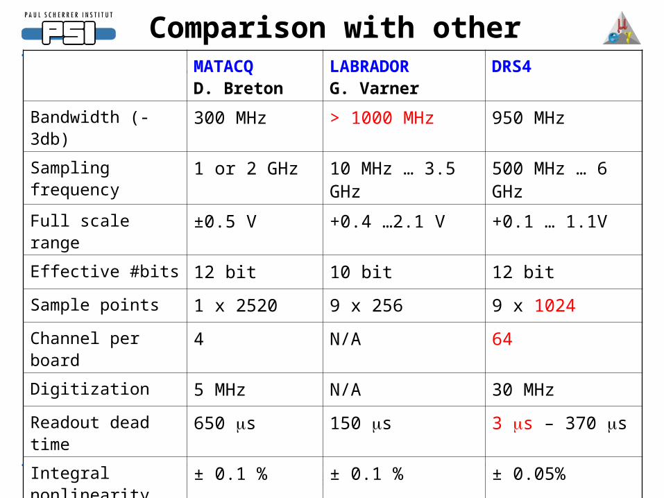
Comparison with other chipsMATACQ
D. BretonLABRADORG. Varner
DRS4
Bandwidth (-3db) 300 MHz > 1000 MHz 950 MHz
Sampling frequency
1 or 2 GHz 10 MHz … 3.5 GHz
500 MHz … 6 GHz
Full scale range ±0.5 V +0.4 …2.1 V +0.1 … 1.1V
Effective #bits 12 bit 10 bit 12 bit
Sample points 1 x 2520 9 x 256 9 x 1024
Channel per board
4 N/A 64
Digitization 5 MHz N/A 30 MHz
Readout dead time
650 s 150 s 3 s – 370 s
Integral nonlinearity
± 0.1 % ± 0.1 % ± 0.05%
Radiation hard No No Yes (chip)
Board V1729 (CAEN)
- planned (CAEN)
Oct. 21st, 2008 IEEE/NSS Dresden 31
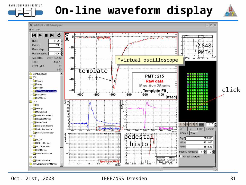
On-line waveform display
click
templatefit
pedestalhisto
848PMTs
“virtual oscilloscope”“virtual oscilloscope”
Oct. 21st, 2008 IEEE/NSS Dresden 32
Lat
ch
Lat
ch
Lat
ch
Lat
ch
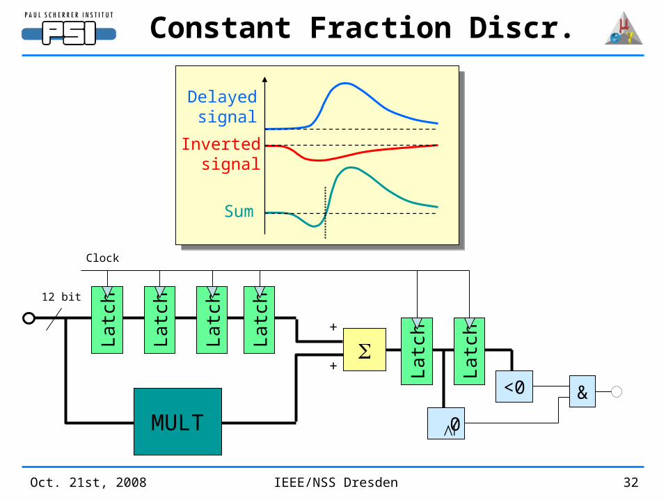
Constant Fraction Discr.
Lat
ch
12 bit
Clock
+
+
MULT
Lat
ch
0
&<0
Delayedsignal
Invertedsignal
Sum