Embed Size (px)
Citation preview
Diplomarbeit
Design and Realizationof Microstrip -Transitions
up to 90GHz
ausgefuhrt zum Zwecke der Erlangung des akademischen Grades eines
Diplom-Ingenieurs unter Leitung von
Werner Simburger und Arpad L. Scholtz
E389
Institut fur Nachrichtentechnik und Hochfrequenztechnik
eingereicht an der Technischen Universitat Wien
Fakultat fur Elektrotechnik und Informationstechnik
von
Georg Lischka
Matrikelnummer: 9525506Kulmgasse 25/13, A-1170 Wien
Wien, im Dezember 2005
Contents
Introduction 1
1 Microstrip to coplanar-V-connector transition 21.1 Design of the microstrip transmission line . . . . . . . . . . . . . 61.2 Optimization of the transition . . . . . . . . . . . . . . . . . . . 71.3 Differential ports . . . . . . . . . . . . . . . . . . . . . . . . . . 91.4 Advanced 2-port calibration with through adapter . . . . . . . . 111.5 Measurement results . . . . . . . . . . . . . . . . . . . . . . . . 131.6 Microwave test-board for chip measurements up to 50GHz . . . 201.7 Manufacturing issues . . . . . . . . . . . . . . . . . . . . . . . . 21
2 Coplanar pads for wafer-probes on microwave substrates 232.1 Coplanar-pads for wafer-probes with ground-vias . . . . . . . . 232.2 Coplanar-pads for wafer-probes with radial stubs . . . . . . . . 272.3 Measurement results . . . . . . . . . . . . . . . . . . . . . . . . 292.4 Further optimization of the coplanar-pads for 77GHz . . . . . . 34
3 Microstrip to waveguide transition at 77 GHz 353.1 State-of-the-art . . . . . . . . . . . . . . . . . . . . . . . . . . . 353.2 Advanced design of a microstrip to waveguide transition . . . . 373.3 Realization . . . . . . . . . . . . . . . . . . . . . . . . . . . . . 443.4 Measurement results . . . . . . . . . . . . . . . . . . . . . . . . 50
Conclusion 55
A Substrate matter constants 56
B Mechanical drawings 63
Bibliography 72
i
ii
Abstract
Aim of this master thesis was to develop different microstrip transmission linetransitions for microwave substrates. The work was done at INFINEON Tech-nologies AG, Corporate Research, Department for High Frequency Circuits(CPR HF), Munich. There on-board measurements are currently limited atabout 18GHz due to the use of SMA-connectors. Measurements at higher fre-quencies are done normally on-chip using a wafer-prober. Using the developedtransitions on-board measurements at higher frequencies will be possible.
Three types of microstrip transitions have been designed and realized: ADC to 50GHz microstrip to coplanar-V-connector transition, a DC to 90GHzcoplanar ground-signal-ground (GSG) probe pad structure for wafer-probes ona microwave substrate and finally a microstrip to waveguide transition opti-mized at 77GHz for the automotive radar frequency band. All three trans-mission line transitions are used in different test fixtures for measurement andcharacterization of microwave integrated circuits.

List of Abbreviations
a Dimension of the broad wall of the waveguideai Normalized complex voltage wave transmitted to the ith portADS Advanced Design System (Agilent)b Dimension of the narrow wall of the waveguidebi Normalized complex voltage wave reflected from the ith portCP Coplanard DistanceDC Direct CurrentDUT Device Under T este Distance between center of the waveguide
and center of the patch antennaεr Relative permittivityεr,eff Effective relative permittivityf FrequencyfRn Resonance frequency
f(o)n Upper 3dB frequency
f(u)n Lower 3dB frequency
g Width of the gapGSG Ground-Signal-GroundGSSG Ground-Signal-Signal-Groundh Heightk Length of the gapl LengthLResonator Length of the resonator∆l Additional effective length at a microstrip openλ Wavelengthλg Wavelength of the cutoff frequencyλ77 Wavelength at 77GHzm Natural numberµ PermeabilityMS M icrostripn Order of the resonance frequency, Natural numberpi Input Powerpo Output PowerQ Q factorQε Q factor caused by tanδε
Qρ Q factor caused by the skin effectqε Dielectric filling factorS S-matrix
iii
~S Poynting vectors Distance between coupled linesSMA SubM iniatur A : Standard RF connector up to 18GHzT T-matrixt Thicknesstanδ Dissipation FactorTL T ransmissionlineu Width of the feeding linev Distance between edge and viasVi Input voltageVo Output voltagew WidthZ¯
Characteristic impedance
iv
Introduction
This master thesis was done at INFINEON Technologies AG, Corporate Re-search, Department for High Frequency Circuits (CPR HF), Munich. Aim ofthis master thesis was to develop different microstrip transmission line tran-sitions for microwave substrates. Currently for on-board measurements SMA-connectors are used there. These connectors are specified up to 18GHz. Mea-surements at higher frequencies are done there on-chip using wafer-probes.Using the developed transitions on-board measurement at higher frequencieswill be possible.
For measurements with coaxial connectors it is desired to measure up to50GHz. The coplanar V-Connector V115FCPW 2.4mm from Anritsu is speci-fied up to 65GHz. Because of the coplanar feeding a transition to a microstriptransmission line is designed here.
For higher frequencies no measurement equipment using coaxial connectors isavailable in the laboratory. The measurement equipment for frequencies up to110GHz is connected to a wafer-prober. It is used for on-chip measurements.On-chip measurements have the disadvantage that the wafer-probes can onlybe placed on pads with a ground-signal-ground (GSG) or ground-signal-signal-ground (GSSG) structure. Also no packaged chip can be measured this way.In order to get a higher flexibility on-board measurements are desired.
Due to the fact that the measurement equipment is connected to the wafer-prober, a transition from a microstrip transmission line to the tips of the wafer-probes is necessary. Therefore coplanar pads on a microwave substrate for thewafer-probes have to be designed. The wafer-prober still will be required, butit will not be necessary to connect the chip directly with the probes.
The wafer probes are very expensive and delicate. For frequently repeated mea-surements also a more insensitive way has to be found. The aim is to measureat 77GHz for the automotive radar frequency band. Therefore a waveguide-to-microstrip-transition is developed here. Finally there should be a networkanalyzer connected to rectangular waveguides instead of a wafer-prober. Theserectangular waveguides should be mounted directly onto the microwave sub-strate.
1

Chapter 1
Microstrip tocoplanar-V-connector transitionfor DC to 50GHz
Currently Rogers RO4003C microwave substrates are widely used for mea-surements. These boards are connected by SMA-connectors (see Fig. 1.1). Dueto the SMA-Connectors measurements are limited at about 18GHz. Also theRogers RO4003C microwave substrate is only specified up to 10GHz.
HUBER+SUHNER® DATA SHEET Coaxial Panel Connector: 23_SMA-50-0-12/111_N Rev.: A
Document: DOC-0000187659 C.00 Issued: Uncontrolled Copy Page 1/1
Description Straight panel receptacle jack, flange mount Interface standards IEC 60169-15_MIL-STD-348A/310_CECC 22110 Technical Data Electrical Data Impedance 50 Ω Interface frequency max. 18 GHz Mechanical Data Weight 0.0021 kg Environmental Data Operating Temperature -65 °C to 165 °C Material Data Piece Parts Material Surface Plating Centre contact Copper Beryllium Alloy Gold Plating (Nickel underplated) Outer contact Copper Beryllium Alloy Gold Plating (Nickel underplated) Body Copper Beryllium Alloy Gold Plating (Nickel underplated) Insulator PFA / PTFE Related Documents Catalogue drawing DCA-00010325 Ordering Information Single package 23_SMA-50-0-12/111_NE
HUBER+SUHNER is certified according to ISO 9001 and ISO 14001
WAIVER! It is exclusively in written agreements that we provide our customers with warrants and representations as to the technical contained specifications and/or the fitness for any particular purpose. The facts and figures herein are carefully compiled to the best of our knowledge, but they are intended for general informational purposes only.
HUBER+SUHNER AG RF Technology 9100 Herisau, Switzerland Phone +41 (0)71 353 41 11 Fax +41 (0)71 353 45 90 www.hubersuhner.com
HUBER+SUHNER – Excellence in Connectivity Solutions
Figure 1.1: Huber&Suhner SMA-Connector 50Ω 23 SMA-50-0-36/11 NE forDC-18GHz
If measurements at higher frequencies are required advanced connector typesand microwave substrates have to be used. Therefore suitable connectors andan appropriate microwave substrate have to be tested. There are differentdesigns from Anritsu for a 2.4mm connector, which are all specified up to65GHz. The available measurement equipment in the laboratory is limited at50GHz, i.e. these connectors fit to our specifications. There is a design fromAnritsu for the direct connection of a microstrip transmission line as well, but itcan not be used here. For our aim it is planned to use a block of aluminium for
2

Chapter 1. Microstrip to coplanar-V-connector transition 3
frequency range DC - 65GHzreturn loss >15dB
Table 1.1: Technical Data Sheet for Anritsu V-Connectors V115FCPW 2.4mm(see Fig. 1.2)
assembling, where the connectors are fixed by screws. (see Fig. 1.4) The blockof aluminum was originally designed for the SMA-connectors. The connectorsdo not have to be soldered and can be reused many times.
Connectors for direct feeding of a microstrip transmission line have both acontact on the top and a ground contact on the bottom of the microwavesubstrate. This means the height of the microwave substrate has to fit theconnector and it has to be soldered as well. Otherwise there will not be agood contact. For this reason it is decided to use the 2.4mm V-ConnectorV115FCPW from Anritsu (see Fig. 1.2 and Tab. 1.1). This connector has acoplanar feeding and can be mounted on the top of the microwave substrate. Inorder to get an electrical contact little mechanical stress is needed. According tothe specification the connectors should be soldered. It has to be tested whetherthey work also without soldering. But now a transition from a coplanar feedingto a microstrip transmission line is necessary.
Figure 1.2: Anritsu 50Ω V-Connectors V115FCPW 2.4mm for DC-65GHz
The transition from an SMA-Connector to a microstrip transmission line on aRogers RO4003C microwave substrate is is easily to design, because the widthof the contact pin and the width of the microstrip transmission line are nearlythe same. But the transition from the 2.4mm V-connector V115FCPW to amicrostrip transmission line on a Rogers RO3003 microwave substrate is more
Chapter 1. Microstrip to coplanar-V-connector transition 4
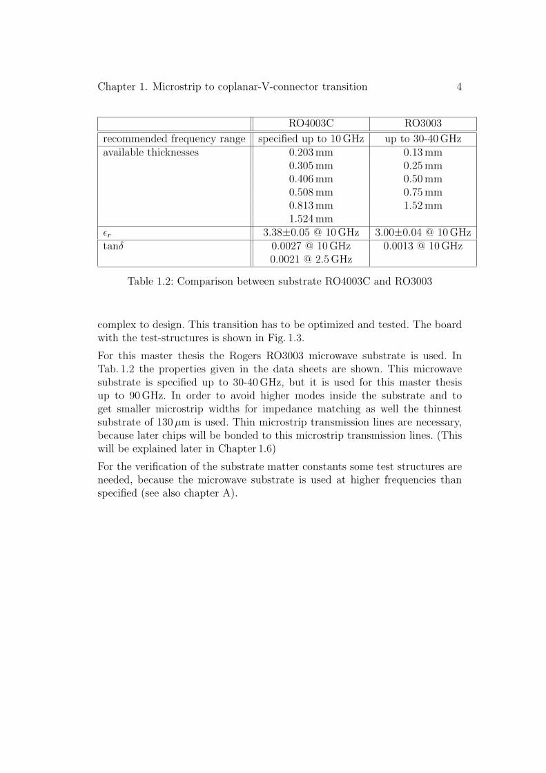
RO4003C RO3003
recommended frequency range specified up to 10GHz up to 30-40GHzavailable thicknesses 0.203mm 0.13mm
0.305mm 0.25mm0.406mm 0.50mm0.508mm 0.75mm0.813mm 1.52mm1.524mm
εr 3.38±0.05 @ 10GHz 3.00±0.04 @ 10GHztanδ 0.0027 @ 10GHz 0.0013 @ 10GHz
0.0021 @ 2.5GHz
Table 1.2: Comparison between substrate RO4003C and RO3003
complex to design. This transition has to be optimized and tested. The boardwith the test-structures is shown in Fig. 1.3.
For this master thesis the Rogers RO3003 microwave substrate is used. InTab. 1.2 the properties given in the data sheets are shown. This microwavesubstrate is specified up to 30-40GHz, but it is used for this master thesisup to 90GHz. In order to avoid higher modes inside the substrate and toget smaller microstrip widths for impedance matching as well the thinnestsubstrate of 130µm is used. Thin microstrip transmission lines are necessary,because later chips will be bonded to this microstrip transmission lines. (Thiswill be explained later in Chapter 1.6)
For the verification of the substrate matter constants some test structures areneeded, because the microwave substrate is used at higher frequencies thanspecified (see also chapter A).

Chapter 1. Microstrip to coplanar-V-connector transition 5
Figure 1.3: Test-board with transitions for the Anritsu V-connectorsV115FCPW and transitions for the measurement with the wafer-prober us-ing a Rogers RO3003-130µm microwave substrate.
Chapter 1. Microstrip to coplanar-V-connector transition 6
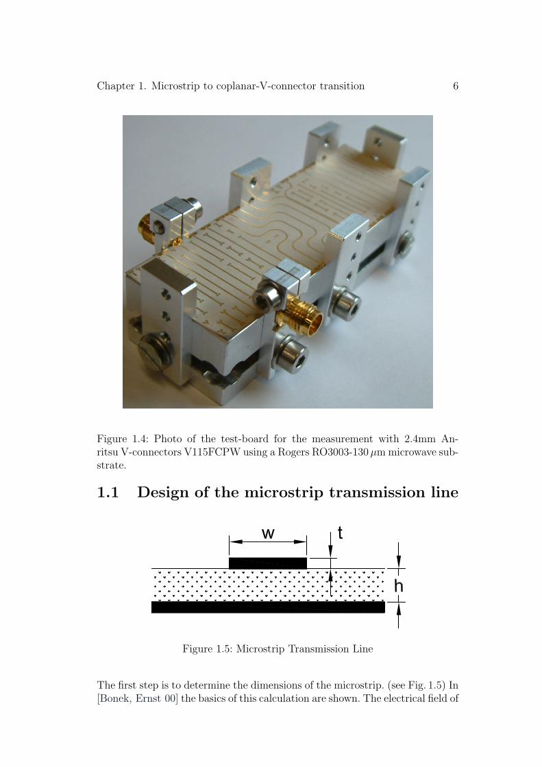
Figure 1.4: Photo of the test-board for the measurement with 2.4mm An-ritsu V-connectors V115FCPW using a Rogers RO3003-130µm microwave sub-strate.
1.1 Design of the microstrip transmission line
Figure 1.5: Microstrip Transmission Line
The first step is to determine the dimensions of the microstrip. (see Fig. 1.5) In[Bonek, Ernst 00] the basics of this calculation are shown. The electrical field of

Chapter 1. Microstrip to coplanar-V-connector transition 7
Simulator optimized width w for Z¯=50Ω
Agilent ADS 2003A 335µmCST Microwave Studio 5.0 315µmSonnet 8.52 350µmTL-Designer 290µm
Table 1.3: Comparison between the optimization results for the best mi-crostrip width w for a 50Ω characteristic impedance for DC-90GHz usinga Rogers RO3003-130µm microwave substrate with copper thickness t=40µm(see Fig. 1.5).
a microstrip transmission line is very inhomogeneous, which leads to a complexcalculation. Optimization of the microstrip is done using the simulators TL-Designer, Advanced Design System ADS, Sonnet and CST Microwave-Studio.TL-Designer is a tool programmed by Franz Weiss [Weiss 04] based on MaxwellSV. Originally the height of the copper t is 17µm. Because of the metal etchingand the epitaxial growth of copper for the via generation the height t increasesto between 30 and 40µm. There is only a low influence of the height t tothe characteristic impedance of a microstrip transmission line, because theelectrical field is mainly inside the substrate. For the electrical losses it hasonly a low influence as well because of the skin effect. However for the designof coupled microstrip transmission lines it has to be taken into account (seeChapter 1.3).
Every simulator returns a lightly different result. The returned value for thewidth w is between 290µm and 350µm for the best matching of the 50Ωcharacteristic impedance. (see Tab. 1.3) For the simulations the given matterconstants from the data-sheet are used. But these parameters (εr, tanδ) areonly specified at 10GHz and the substrate is only specified for frequencies upto 30-40GHz. So it is not known how much these matter constants will changeat higher frequencies.
Therefore different designs with 4 different widths of the microstrip are de-signed. The used widths are 275µm, 300µm, 325µm and 350µm.
1.2 Optimization of the transition
For the Anritsu V-connector V115FCPW shown in Fig. 1.2 a GSG-contacthas to be designed. The connector has a distance of 760µm between the twoground contacts. A mechanical tolerance of 100µm for assembling is desired.Therefore the width of the ground-pads has to be increased by 100µm on bothsides. Thus the distance between the two ground pads becomes 560µm. Thisleads to a width of the signal-line of about 260µm for impedance matching.
Chapter 1. Microstrip to coplanar-V-connector transition 8
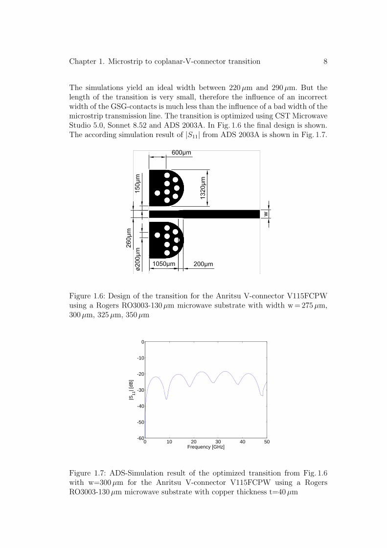
The simulations yield an ideal width between 220µm and 290µm. But thelength of the transition is very small, therefore the influence of an incorrectwidth of the GSG-contacts is much less than the influence of a bad width of themicrostrip transmission line. The transition is optimized using CST MicrowaveStudio 5.0, Sonnet 8.52 and ADS 2003A. In Fig. 1.6 the final design is shown.The according simulation result of |S11| from ADS 2003A is shown in Fig. 1.7.
Figure 1.6: Design of the transition for the Anritsu V-connector V115FCPWusing a Rogers RO3003-130µm microwave substrate with width w=275µm,300µm, 325µm, 350µm
0 10 20 30 40 50-60
-50
-40
-30
-20
-10
0
Frequency [GHz]
|S11
| [dB
]
Figure 1.7: ADS-Simulation result of the optimized transition from Fig. 1.6with w=300µm for the Anritsu V-connector V115FCPW using a RogersRO3003-130µm microwave substrate with copper thickness t=40µm

Chapter 1. Microstrip to coplanar-V-connector transition 9
1.3 Differential ports
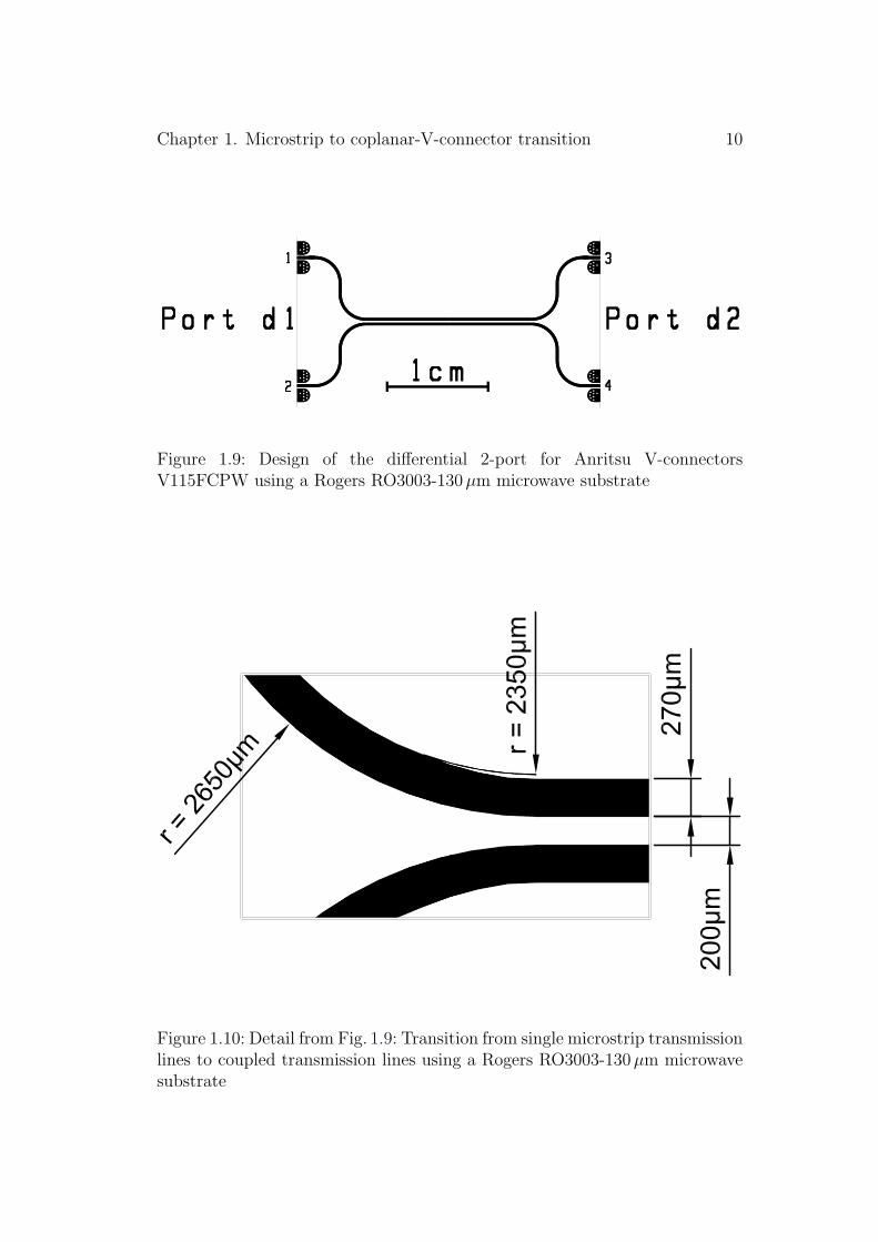
At high frequencies normally differential signals are used. The signal lineshave to be bonded to the chip. In order to get a good transition to the bondwires, coupled lines are needed (see Fig. 1.8). TIt has to be mentioned that thecharacteristic impedance depends strongly on the gap s between the microstriplines. The minimum distance because of production processes is 100µm, butbecause of tolerances in the production this would lead to too high tolerancesof the characteristic impedance. Therefore a gap of 200µm is selected. Thisleads to coupled striplines with a width of about 270µm. The transition fromthe separated microstrip lines to the coupled microstrip lines is optimized usingADS (see Fig. 1.10).
The final design is shown later in Fig. 1.24. For the measurement of the differ-ential S-parameters of the coupled lines a differential 2-port is necessary (seeFig. 1.9).
We can not measure differential S-parameters directly. In the laboratory thereis only a 2-port network analyzer for conventional S-parameters. But we canregard this differential 2-port as a normal 4-port. There six different 2-portmeasurements have to be done, where the ports not connected have to beterminated. Out of these results we can calculate the differential S-Parametersfor the differential ports d1 and d2 using the formulas (1.1)-(1.4) (see also[Pollendorfer 04], [Anritsu 01]).
Figure 1.8: Coupled microstrip transmission lines
Sd1d1 =1
2(S11 − S21 − S12 + S22) (1.1)
Sd1d2 =1
2(S13 − S23 − S14 + S24) (1.2)
Sd2d1 =1
2(S31 − S41 − S32 + S42) (1.3)
Sd2d2 =1
2(S33 − S43 − S34 + S44) (1.4)
Chapter 1. Microstrip to coplanar-V-connector transition 10
Figure 1.9: Design of the differential 2-port for Anritsu V-connectorsV115FCPW using a Rogers RO3003-130µm microwave substrate
Figure 1.10: Detail from Fig. 1.9: Transition from single microstrip transmissionlines to coupled transmission lines using a Rogers RO3003-130µm microwavesubstrate

Chapter 1. Microstrip to coplanar-V-connector transition 11
Figure 1.11: Ideal situation for calibration: one connector is male the other isfemal
Figure 1.12: Through calibration for the measurement from Fig. 1.11
1.4 Advanced 2-port calibration with through
adapter
For a 2-port-calibration the reflections of the two ports and the transmissionshave to be measured. This will work correctly, if the connector of one portis male and the other is female (see Fig. 1.11 and Fig. 1.12). If both connec-tors are male, an adapter will be necessary to connect them (see Fig. 1.13).So the reference planes of the reflection measurements do not fit together atthe transmission measurement. This normally is compensated by defining anelectrical delay. But this leads to a calibration error, because the losses of theadapter are ignored. Normally this calibration is good enough, but not in thiscase. We want to verify the losses of the Anritsu V-connectors, therefore anadvanced calibration is needed.
The HP8510B network analyzer is using a feature, which is called ”AdapterRemoval”. The according explanation can be found in [Agilent 00].
Here the calibration has to be done twice. For the first calibration the adapterhas to be connected to the cable of Port 2, so Port 1 can be calibrated correctly.Thus the reference planes fit together at the through-calibration (see Fig. 1.14:Port 1 and Port 2’). Then the calibration has to be repeated, while the adapteris connected to the cable of Port 1. This leads to a correct calibration of Port 2(see Fig. 1.15: Port 1’ and Port 2). Using these two calibration sets, the networkanalyzer can calculate a new calibration set, where the influence of the adapteris removed. This means that there is now a correct calibration.

Chapter 1. Microstrip to coplanar-V-connector transition 12
Figure 1.13: Problem for calibration: non-insertable device (DUT with connec-tors of the same sex)
Figure 1.14: Adapter-removal calibration: correct calibration for port 1
Figure 1.15: Adapter-removal calibration: correct calibration for port 2
Chapter 1. Microstrip to coplanar-V-connector transition 13
1.5 Measurement results
Measurement Equipment
• Network Analyzer for 45MHz-50GHzconsists of the following devices:
- Network Analyzer HP8510B
- Series Synthesized Frequency Sweeper HP83650A for 10MHz-50GHz
- S-Parameter Test Set HP8517A for 45MHz-50GHz
• Calibration Kit Agilent 85056D 2.4mm DC-50GHz
• Calibration Kit Agilent 85052C 3.5mm DC-26.5GHz
Impedance matching
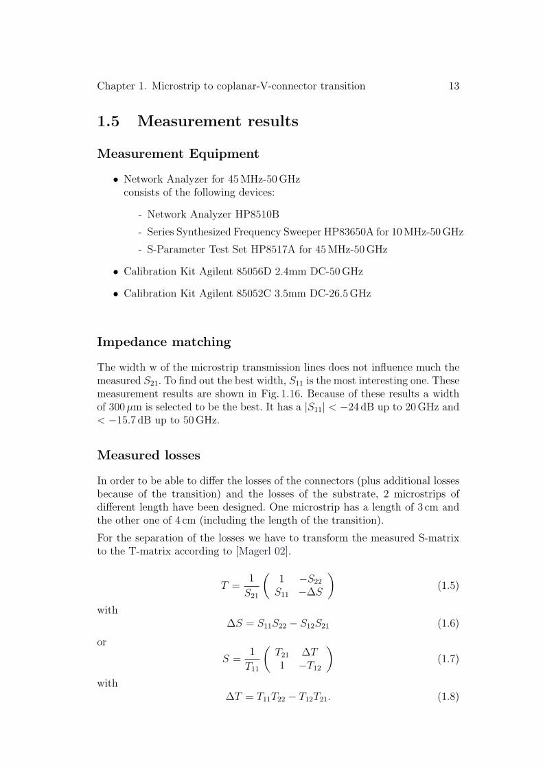
The width w of the microstrip transmission lines does not influence much themeasured S21. To find out the best width, S11 is the most interesting one. Thesemeasurement results are shown in Fig. 1.16. Because of these results a widthof 300µm is selected to be the best. It has a |S11| < −24 dB up to 20GHz and< −15.7 dB up to 50GHz.
Measured losses
In order to be able to differ the losses of the connectors (plus additional lossesbecause of the transition) and the losses of the substrate, 2 microstrips ofdifferent length have been designed. One microstrip has a length of 3 cm andthe other one of 4 cm (including the length of the transition).
For the separation of the losses we have to transform the measured S-matrixto the T-matrix according to [Magerl 02].
T =1
S21
(1 −S22
S11 −∆S
)(1.5)
with∆S = S11S22 − S12S21 (1.6)
or
S =1
T11
(T21 ∆T1 −T12
)(1.7)
with∆T = T11T22 − T12T21. (1.8)
Chapter 1. Microstrip to coplanar-V-connector transition 14
0 10 20 30 40 50-50
-45
-40
-35
-30
-25
-20
-15
-10
Frequency [GHz]
|S11
| [dB
]
w=275μmw=300μmw=325μmw=350μm
Figure 1.16: Measured |S11| of the microstrip transmission lines (withlength l=3 cm) with different widths connected by the Anritsu V-ConnectorsV115FCPW and using a Rogers RO3003-130µm microwave substrate (seeFig. 1.3)
Now the T-matrix of two 2-ports in series can be calculated by
T = TA·TB. (1.9)
Using the T-matrix we can calculate the S-parameter of 2-ports in series. An-alyzing this formulas some approximations can be done to simplify the calcu-lation. First the matrix of the 3 cm microstrip line is divided into two parts
T3cm = TA·TB. (1.10)
Then also the 4 cm microstrip line is divided
T3cm = TA·T1cm·TB. (1.11)
According to Fig. 1.16 and Fig. 1.17 |S11||S21|, therefore for the calculationof the losses S11 is set to 0. This approximation leads to
S(4cm)21 = S
(A)21 ·S
(1cm)21 ·S(B)
21 (1.12)

Chapter 1. Microstrip to coplanar-V-connector transition 15
0 10 20 30 40 50-4.5
-4
-3.5
-3
-2.5
-2
-1.5
-1
-0.5
0
Frequency [GHz]
|S21
| [dB
]
S21(3cm)S21(4cm)S21(4cm) - S21(3cm)
Figure 1.17: Measured |S21| of the microstrip transmission lines (with widthw=300µm) with different lengths connected by the Anritsu V-ConnectorsV115FCPW and using a Rogers RO3003-130µm microwave substrate (seeFig. 1.3)
and further toS
(1cm)21 [dB] = S
(4cm)21 [dB]− S
(3cm)21 [dB]. (1.13)
The difference of |S21| of this two microstrip transmission lines is nearly equiv-alent to the losses per centimeter. In Fig. 1.17 the results of these measure-ments are shown. The losses of the microstrip on the Rogers RO3003 sub-strate are about 0.9 dB/cm at 50GHz. The losses of the connectors plus theadditional losses because of the transition can be calculated out of these mea-surements and are about 0.2 dB/connector for the full frequency range fromDC to 50GHz.
Measurement Results of the differential ports
The calculated |Sd1d1| and |Sd2d1| out of the measurement results are shown inFig. 1.18 and Fig. 1.19. The whole length of the striplines is about 35.7mm.The measured losses also fit approximately to the expected losses according toFig. 1.17.

Chapter 1. Microstrip to coplanar-V-connector transition 16
0 10 20 30 40 50-55
-50
-45
-40
-35
-30
-25
-20
-15
Frequency [GHz]
|Sd1
d1| [
dB]
Figure 1.18: Measured reflection of the differential 2-port connected by the An-ritsu V-connectors V115FCPW and using a Rogers RO3003-130µm microwavesubstrate (see Fig. 1.9 and Fig. 1.10)
0 10 20 30 40 50-4
-3.5
-3
-2.5
-2
-1.5
-1
-0.5
0
Frequency [GHz]
|Sd2
d1| [
dB]
Figure 1.19: Measured transmission of the differential 2-port connected bythe Anritsu V-connectors V115FCPW and using a Rogers RO3003-130µmmicrowave substrate (see Fig. 1.9 and Fig. 1.10)
Chapter 1. Microstrip to coplanar-V-connector transition 17
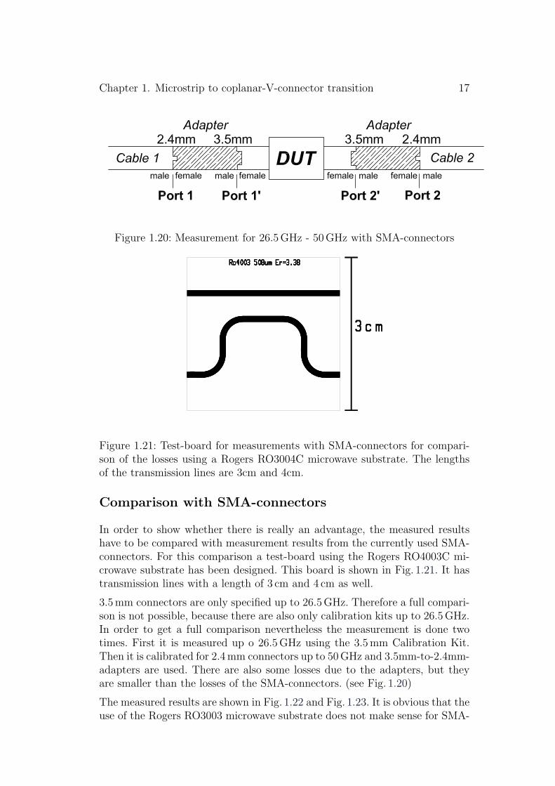
Figure 1.20: Measurement for 26.5GHz - 50GHz with SMA-connectors
Figure 1.21: Test-board for measurements with SMA-connectors for compari-son of the losses using a Rogers RO3004C microwave substrate. The lengthsof the transmission lines are 3cm and 4cm.
Comparison with SMA-connectors
In order to show whether there is really an advantage, the measured resultshave to be compared with measurement results from the currently used SMA-connectors. For this comparison a test-board using the Rogers RO4003C mi-crowave substrate has been designed. This board is shown in Fig. 1.21. It hastransmission lines with a length of 3 cm and 4 cm as well.
3.5mm connectors are only specified up to 26.5GHz. Therefore a full compari-son is not possible, because there are also only calibration kits up to 26.5GHz.In order to get a full comparison nevertheless the measurement is done twotimes. First it is measured up o 26.5GHz using the 3.5mm Calibration Kit.Then it is calibrated for 2.4mm connectors up to 50GHz and 3.5mm-to-2.4mm-adapters are used. There are also some losses due to the adapters, but theyare smaller than the losses of the SMA-connectors. (see Fig. 1.20)
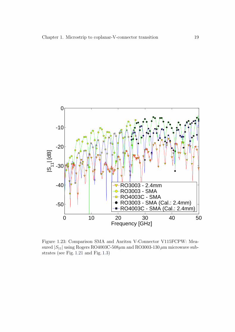
The measured results are shown in Fig. 1.22 and Fig. 1.23. It is obvious that theuse of the Rogers RO3003 microwave substrate does not make sense for SMA-

Chapter 1. Microstrip to coplanar-V-connector transition 18
0 10 20 30 40 50-8
-7
-6
-5
-4
-3
-2
-1
0
Frequency [GHz]
|S21
| [dB
]
RO3003 - 2.4mmRO3003 - SMARO4003C - SMARO3003 - SMA (Cal.: 2.4mm)RO4003C - SMA (Cal.: 2.4mm)
Figure 1.22: Comparison SMA and Anritsu V-Connector V115FCPW: Mea-sured |S21| using Rogers RO4003C-508µm and RO3003-130µm microwave sub-strates (see Fig. 1.21 and Fig. 1.3)
connectors. The result is worse than that with the cheaper Rogers RO4003C.One reason is that the microstrip on the Rogers RO3003-130µm microwavesubstrate has a width of 300µm, but the signal pin of the SMA-connectorhas a width of about 1mm. So the impedance matching at the contact is verybad. The microstrip on the Rogers RO4003C-508µm microwave substrate has awidth of 1160µm, so there is much less impedance mismatch. Also the electricallosses on the microstrip are less if the width is larger.
For frequencies up to 20GHz the use of SMA-connectors together with theRogers RO4003C microwave substrate should be preferred. But for frequen-cies from 25GHz to 50GHz the measurement with the Anritsu V-connectortogether with the Rogers RO3003 microwave substrate leads to better results.
Chapter 1. Microstrip to coplanar-V-connector transition 19
0 10 20 30 40 50
-50
-40
-30
-20
-10
0
Frequency [GHz]
|S11
| [dB
]
RO3003 - 2.4mmRO3003 - SMARO4003C - SMARO3003 - SMA (Cal.: 2.4mm) RO4003C - SMA (Cal.: 2.4mm)
Figure 1.23: Comparison SMA and Anritsu V-Connector V115FCPW: Mea-sured |S11| using Rogers RO4003C-508µm and RO3003-130µm microwave sub-strates (see Fig. 1.21 and Fig. 1.3)
Chapter 1. Microstrip to coplanar-V-connector transition 20
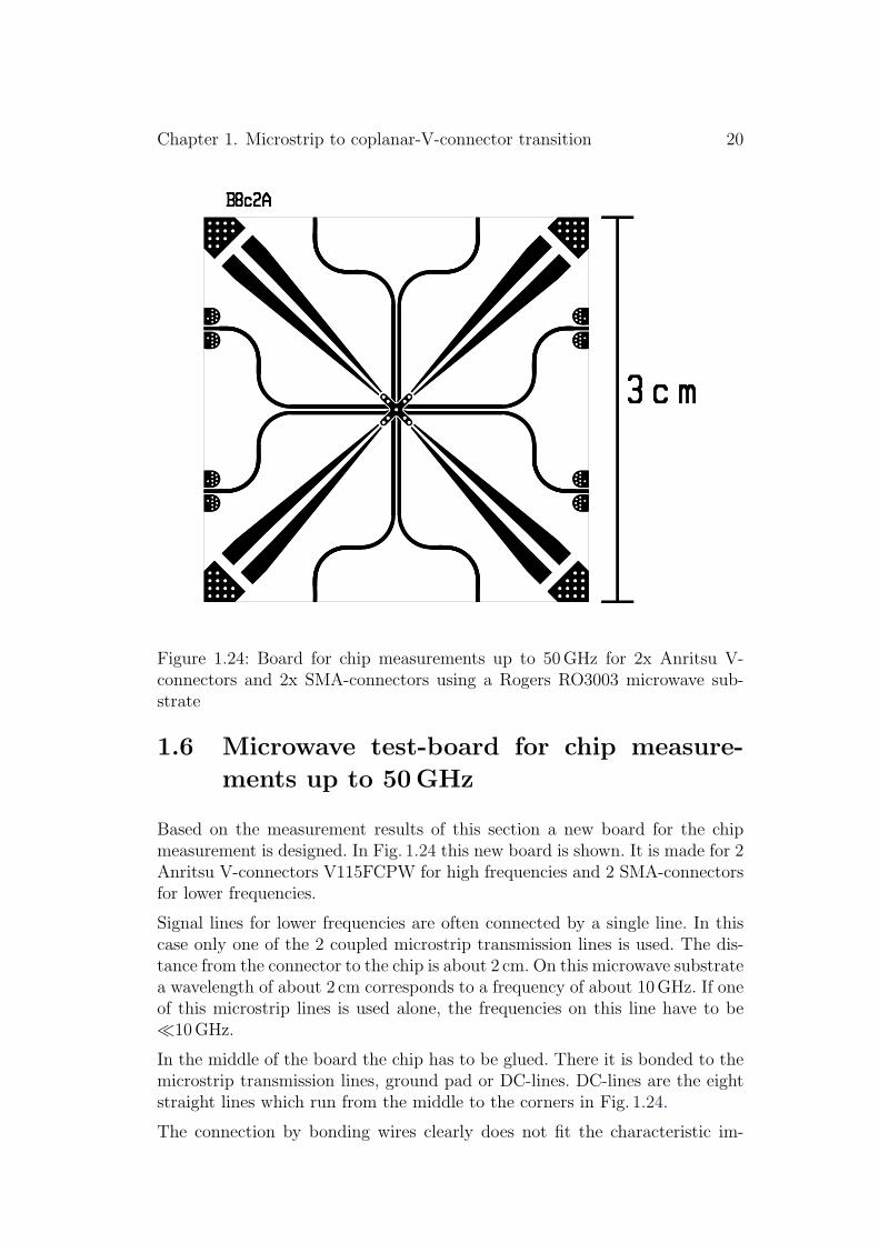
Figure 1.24: Board for chip measurements up to 50GHz for 2x Anritsu V-connectors and 2x SMA-connectors using a Rogers RO3003 microwave sub-strate
1.6 Microwave test-board for chip measure-
ments up to 50 GHz
Based on the measurement results of this section a new board for the chipmeasurement is designed. In Fig. 1.24 this new board is shown. It is made for 2Anritsu V-connectors V115FCPW for high frequencies and 2 SMA-connectorsfor lower frequencies.
Signal lines for lower frequencies are often connected by a single line. In thiscase only one of the 2 coupled microstrip transmission lines is used. The dis-tance from the connector to the chip is about 2 cm. On this microwave substratea wavelength of about 2 cm corresponds to a frequency of about 10GHz. If oneof this microstrip lines is used alone, the frequencies on this line have to be10GHz.
In the middle of the board the chip has to be glued. There it is bonded to themicrostrip transmission lines, ground pad or DC-lines. DC-lines are the eightstraight lines which run from the middle to the corners in Fig. 1.24.
The connection by bonding wires clearly does not fit the characteristic im-
Chapter 1. Microstrip to coplanar-V-connector transition 21
pedance of 50Ω. Also at the end of the coupled microstrip transmission linesthere is a impedance mismatch. But as long as this distance is very small incomparison to the wavelength, it has only a small influence. Therefore thintransmission lines are needed.
1.7 Manufacturing issues
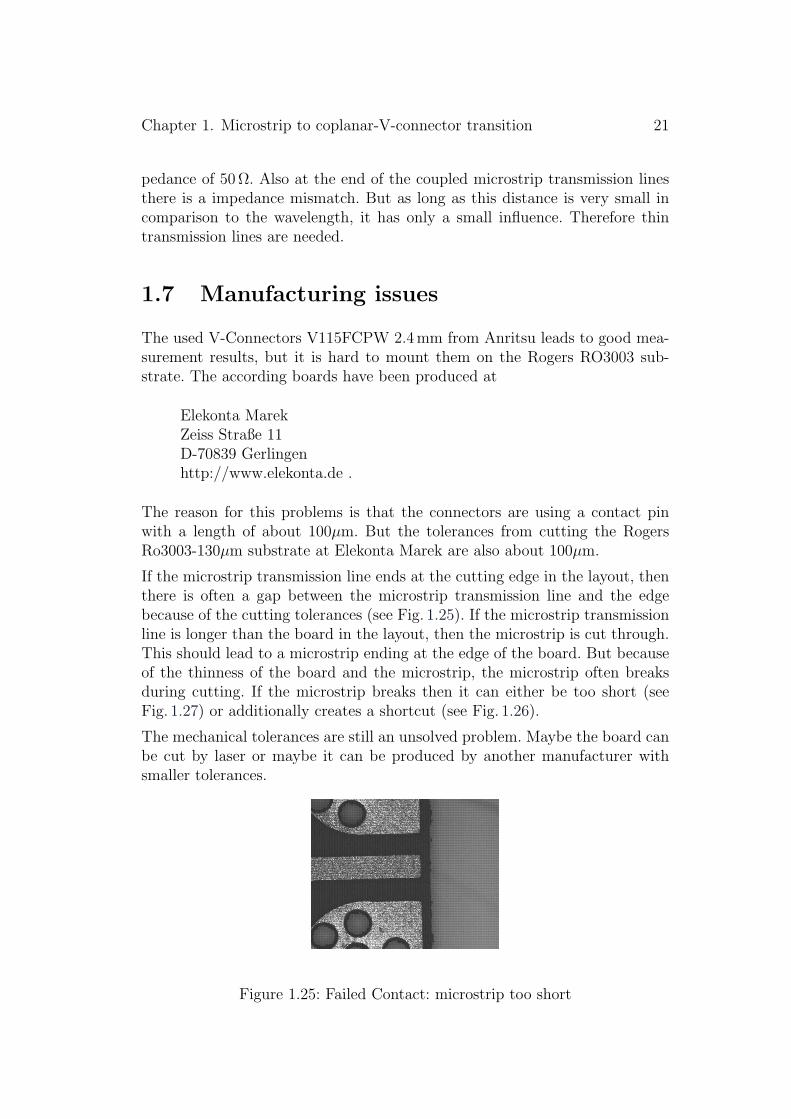
The used V-Connectors V115FCPW 2.4mm from Anritsu leads to good mea-surement results, but it is hard to mount them on the Rogers RO3003 sub-strate. The according boards have been produced at
Elekonta MarekZeiss Straße 11D-70839 Gerlingenhttp://www.elekonta.de .
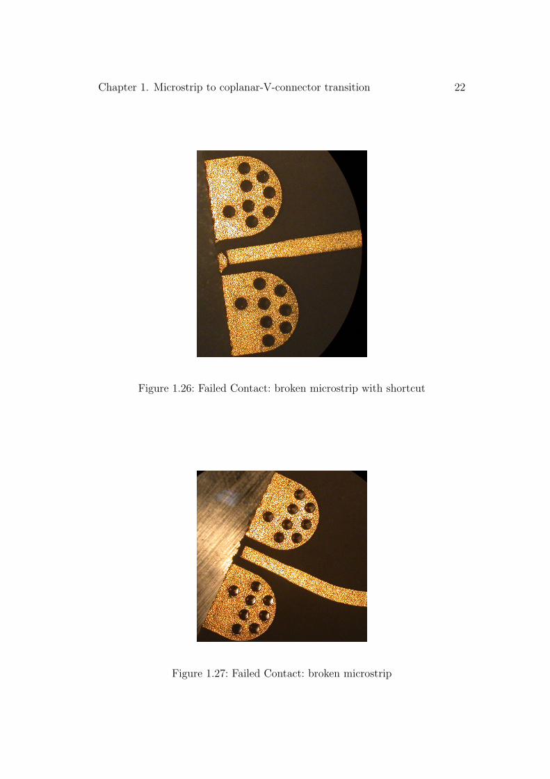
The reason for this problems is that the connectors are using a contact pinwith a length of about 100µm. But the tolerances from cutting the RogersRo3003-130µm substrate at Elekonta Marek are also about 100µm.
If the microstrip transmission line ends at the cutting edge in the layout, thenthere is often a gap between the microstrip transmission line and the edgebecause of the cutting tolerances (see Fig. 1.25). If the microstrip transmissionline is longer than the board in the layout, then the microstrip is cut through.This should lead to a microstrip ending at the edge of the board. But becauseof the thinness of the board and the microstrip, the microstrip often breaksduring cutting. If the microstrip breaks then it can either be too short (seeFig. 1.27) or additionally creates a shortcut (see Fig. 1.26).
The mechanical tolerances are still an unsolved problem. Maybe the board canbe cut by laser or maybe it can be produced by another manufacturer withsmaller tolerances.
Figure 1.25: Failed Contact: microstrip too short
Chapter 1. Microstrip to coplanar-V-connector transition 22
Figure 1.26: Failed Contact: broken microstrip with shortcut
Figure 1.27: Failed Contact: broken microstrip

Chapter 2
Coplanar pads for wafer-probeson microwave substrates up to90 GHz
Measurements up to 110GHz are currently done on-chip with wafer-probes.But it is not always possible to contact the chip with wafer-probes directly.Therefore a possibility has to be found to measure on-board at high frequencies.For these measurements coplanar pads on a microwave substrate have to bedesigned. Here the Rogers RO3003-130µm microwave substrate is used again.Therefore the according test-structures are on the same test-board as for theAnritsu-V-Connectors. (see Fig. 1.3)
The available wafer-probes can be used up to 90GHz. But the Rogers RO3003microwave substrate is only specified up to 30-40GHz (see Tab. 1.2). Becausethe microwave substrate is used at higher frequencies than specified, the sub-strate matter constants have to be verified (see also chapterA). The losses upto 50GHz are also measured in chapter 1.5 using Anritsu V-connectors. From50GHz to 90GHz the verification has to be done using the wafer-prober.
The width of the microstrip transmission lines has been calculated already inChapter 1.1.
2.1 Coplanar-pads for wafer-probes with
ground-vias
The first task of the wafer-prober measurement is to find a suitable pitch ofthe wafer-probes before the pads can be designed.
To get low reflections a transition with a characteristic impedance of 50Ω isneeded. A GSG-structure on the Rogers RO3003-130µm microwave substrateneeds a signal line of about 220µm with a gap of 100µm. Because of the
23
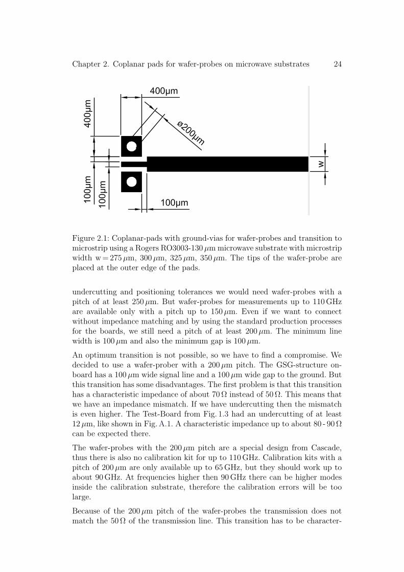
Chapter 2. Coplanar pads for wafer-probes on microwave substrates 24
Figure 2.1: Coplanar-pads with ground-vias for wafer-probes and transition tomicrostrip using a Rogers RO3003-130µm microwave substrate with microstripwidth w=275µm, 300µm, 325µm, 350µm. The tips of the wafer-probe areplaced at the outer edge of the pads.
undercutting and positioning tolerances we would need wafer-probes with apitch of at least 250µm. But wafer-probes for measurements up to 110GHzare available only with a pitch up to 150µm. Even if we want to connectwithout impedance matching and by using the standard production processesfor the boards, we still need a pitch of at least 200µm. The minimum linewidth is 100µm and also the minimum gap is 100µm.
An optimum transition is not possible, so we have to find a compromise. Wedecided to use a wafer-prober with a 200µm pitch. The GSG-structure on-board has a 100µm wide signal line and a 100µm wide gap to the ground. Butthis transition has some disadvantages. The first problem is that this transitionhas a characteristic impedance of about 70Ω instead of 50Ω. This means thatwe have an impedance mismatch. If we have undercutting then the mismatchis even higher. The Test-Board from Fig. 1.3 had an undercutting of at least12µm, like shown in Fig. A.1. A characteristic impedance up to about 80 - 90Ωcan be expected there.
The wafer-probes with the 200µm pitch are a special design from Cascade,thus there is also no calibration kit for up to 110GHz. Calibration kits with apitch of 200µm are only available up to 65GHz, but they should work up toabout 90GHz. At frequencies higher then 90GHz there can be higher modesinside the calibration substrate, therefore the calibration errors will be toolarge.
Because of the 200µm pitch of the wafer-probes the transmission does notmatch the 50Ω of the transmission line. This transition has to be character-
Chapter 2. Coplanar pads for wafer-probes on microwave substrates 25
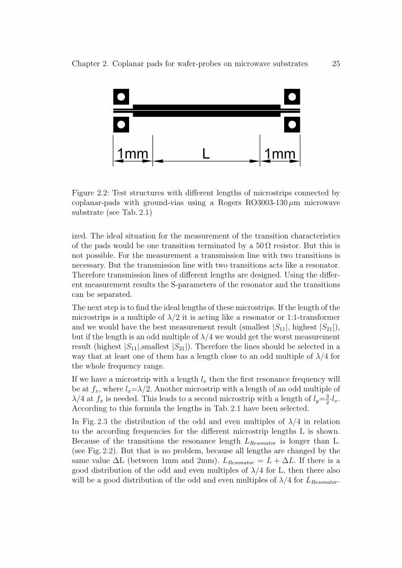
Figure 2.2: Test structures with different lengths of microstrips connected bycoplanar-pads with ground-vias using a Rogers RO3003-130µm microwavesubstrate (see Tab. 2.1)
ized. The ideal situation for the measurement of the transition characteristicsof the pads would be one transition terminated by a 50Ω resistor. But this isnot possible. For the measurement a transmission line with two transitions isnecessary. But the transmission line with two transitions acts like a resonator.Therefore transmission lines of different lengths are designed. Using the differ-ent measurement results the S-parameters of the resonator and the transitionscan be separated.
The next step is to find the ideal lengths of these microstrips. If the length of themicrostrips is a multiple of λ/2 it is acting like a resonator or 1:1-transformerand we would have the best measurement result (smallest |S11|, highest |S21|),but if the length is an odd multiple of λ/4 we would get the worst measurementresult (highest |S11|,smallest |S21|). Therefore the lines should be selected in away that at least one of them has a length close to an odd multiple of λ/4 forthe whole frequency range.
If we have a microstrip with a length lx then the first resonance frequency willbe at fx, where lx=λ/2. Another microstrip with a length of an odd multiple ofλ/4 at fx is needed. This leads to a second microstrip with a length of ly=
32·lx.
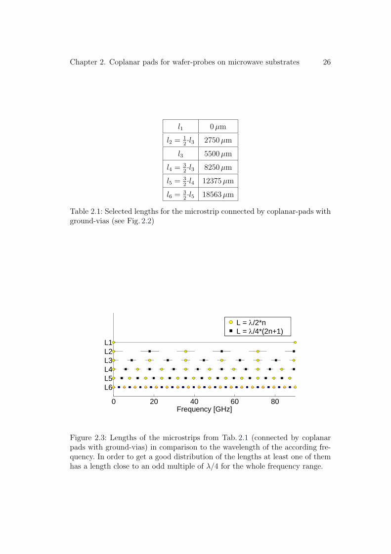
According to this formula the lengths in Tab. 2.1 have been selected.
In Fig. 2.3 the distribution of the odd and even multiples of λ/4 in relationto the according frequencies for the different microstrip lengths L is shown.Because of the transitions the resonance length LResonator is longer than L.(see Fig. 2.2). But that is no problem, because all lengths are changed by thesame value ∆L (between 1mm and 2mm). LResonator = L + ∆L. If there is agood distribution of the odd and even multiples of λ/4 for L, then there alsowill be a good distribution of the odd and even multiples of λ/4 for LResonator.
Chapter 2. Coplanar pads for wafer-probes on microwave substrates 26
l1 0µm
l2 = 12·l3 2750µm
l3 5500µm
l4 = 32·l3 8250µm
l5 = 32·l4 12375µm
l6 = 32·l5 18563µm
Table 2.1: Selected lengths for the microstrip connected by coplanar-pads withground-vias (see Fig. 2.2)
0 20 40 60 80
L6L5L4L3L2L1
Frequency [GHz]
L = λ/2*nL = λ/4*(2n+1) .
Figure 2.3: Lengths of the microstrips from Tab. 2.1 (connected by coplanarpads with ground-vias) in comparison to the wavelength of the according fre-quency. In order to get a good distribution of the lengths at least one of themhas a length close to an odd multiple of λ/4 for the whole frequency range.
Chapter 2. Coplanar pads for wafer-probes on microwave substrates 27
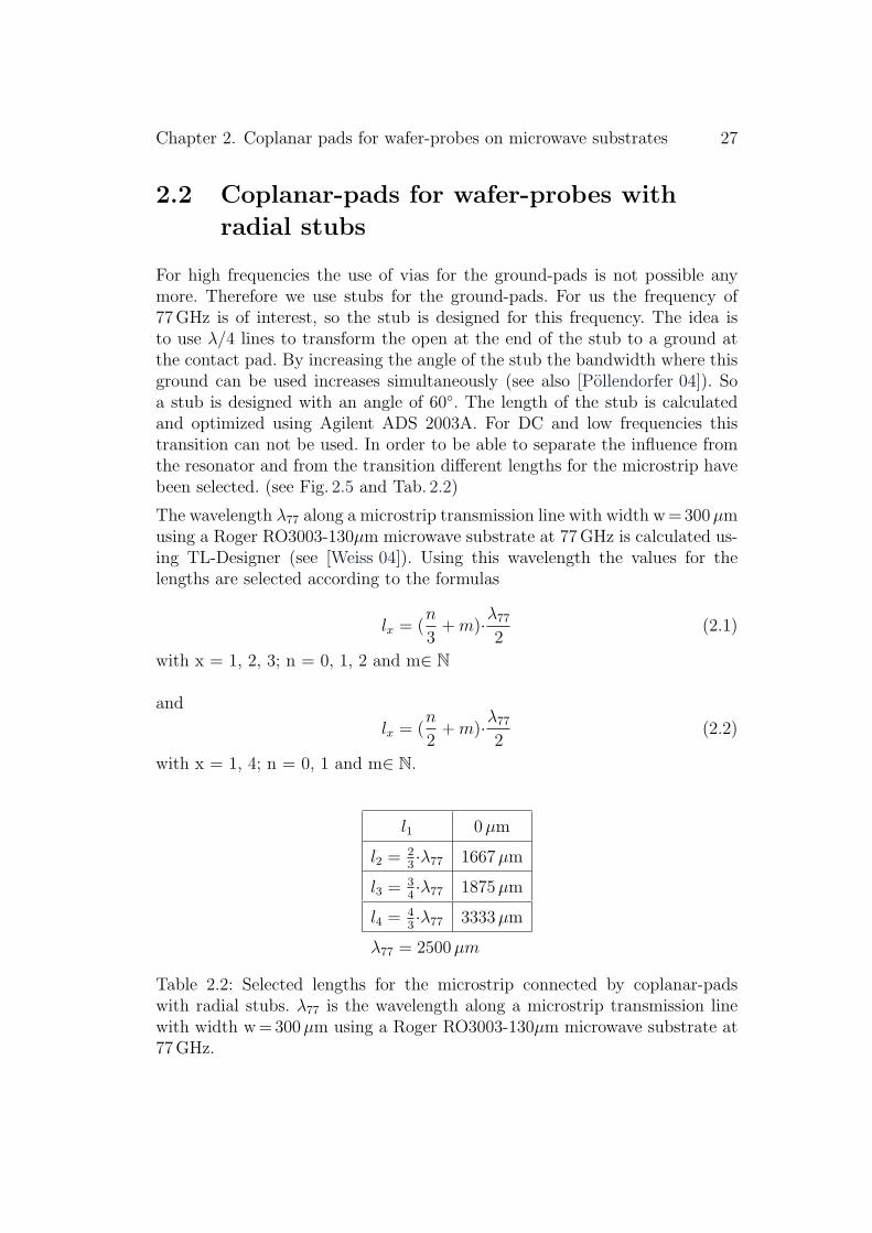
2.2 Coplanar-pads for wafer-probes with
radial stubs
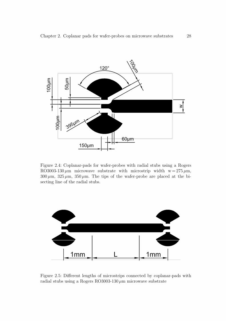
For high frequencies the use of vias for the ground-pads is not possible anymore. Therefore we use stubs for the ground-pads. For us the frequency of77GHz is of interest, so the stub is designed for this frequency. The idea isto use λ/4 lines to transform the open at the end of the stub to a ground atthe contact pad. By increasing the angle of the stub the bandwidth where thisground can be used increases simultaneously (see also [Pollendorfer 04]). Soa stub is designed with an angle of 60. The length of the stub is calculatedand optimized using Agilent ADS 2003A. For DC and low frequencies thistransition can not be used. In order to be able to separate the influence fromthe resonator and from the transition different lengths for the microstrip havebeen selected. (see Fig. 2.5 and Tab. 2.2)
The wavelength λ77 along a microstrip transmission line with width w =300µmusing a Roger RO3003-130µm microwave substrate at 77GHz is calculated us-ing TL-Designer (see [Weiss 04]). Using this wavelength the values for thelengths are selected according to the formulas
lx = (n
3+ m)·λ77
2(2.1)
with x = 1, 2, 3; n = 0, 1, 2 and m∈ N
and
lx = (n
2+ m)·λ77
2(2.2)
with x = 1, 4; n = 0, 1 and m∈ N.
l1 0µm
l2 = 23·λ77 1667µm
l3 = 34·λ77 1875µm
l4 = 43·λ77 3333µm
λ77 = 2500 µm
Table 2.2: Selected lengths for the microstrip connected by coplanar-padswith radial stubs. λ77 is the wavelength along a microstrip transmission linewith width w=300µm using a Roger RO3003-130µm microwave substrate at77GHz.
Chapter 2. Coplanar pads for wafer-probes on microwave substrates 28
Figure 2.4: Coplanar-pads for wafer-probes with radial stubs using a RogersRO3003-130µm microwave substrate with microstrip width w =275µm,300µm, 325µm, 350µm. The tips of the wafer-probe are placed at the bi-secting line of the radial stubs.
Figure 2.5: Different lengths of microstrips connected by coplanar-pads withradial stubs using a Rogers RO3003-130µm microwave substrate
Chapter 2. Coplanar pads for wafer-probes on microwave substrates 29
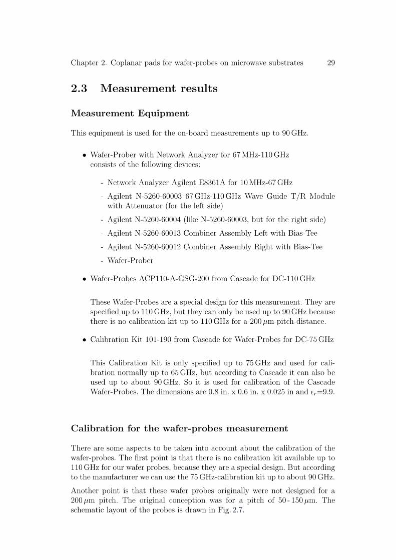
2.3 Measurement results
Measurement Equipment
This equipment is used for the on-board measurements up to 90GHz.
• Wafer-Prober with Network Analyzer for 67MHz-110GHzconsists of the following devices:
- Network Analyzer Agilent E8361A for 10MHz-67GHz
- Agilent N-5260-60003 67GHz-110GHz Wave Guide T/R Modulewith Attenuator (for the left side)
- Agilent N-5260-60004 (like N-5260-60003, but for the right side)
- Agilent N-5260-60013 Combiner Assembly Left with Bias-Tee
- Agilent N-5260-60012 Combiner Assembly Right with Bias-Tee
- Wafer-Prober
• Wafer-Probes ACP110-A-GSG-200 from Cascade for DC-110GHz
These Wafer-Probes are a special design for this measurement. They arespecified up to 110GHz, but they can only be used up to 90GHz becausethere is no calibration kit up to 110GHz for a 200µm-pitch-distance.
• Calibration Kit 101-190 from Cascade for Wafer-Probes for DC-75GHz
This Calibration Kit is only specified up to 75GHz and used for cali-bration normally up to 65GHz, but according to Cascade it can also beused up to about 90GHz. So it is used for calibration of the CascadeWafer-Probes. The dimensions are 0.8 in. x 0.6 in. x 0.025 in and εr=9.9.
Calibration for the wafer-probes measurement
There are some aspects to be taken into account about the calibration of thewafer-probes. The first point is that there is no calibration kit available up to110GHz for our wafer probes, because they are a special design. But accordingto the manufacturer we can use the 75GHz-calibration kit up to about 90GHz.
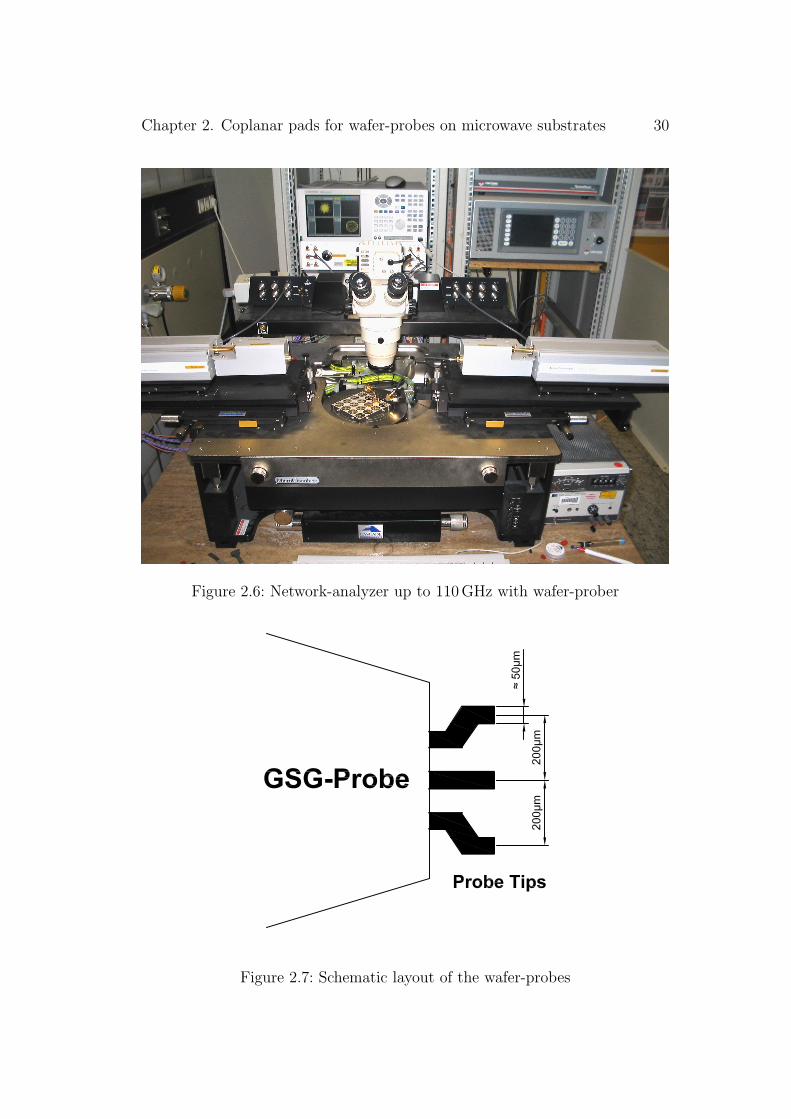
Another point is that these wafer probes originally were not designed for a200µm pitch. The original conception was for a pitch of 50 - 150µm. Theschematic layout of the probes is drawn in Fig. 2.7.
Chapter 2. Coplanar pads for wafer-probes on microwave substrates 30
Figure 2.6: Network-analyzer up to 110GHz with wafer-prober
Figure 2.7: Schematic layout of the wafer-probes

Chapter 2. Coplanar pads for wafer-probes on microwave substrates 31
Measurement results of the coplanar pads with ground-vias
We can see in Fig. 2.8 that this transition works well up to about 30GHz, alsoin Fig. 2.9 we can see that |S11| is ≤-20dB up to 30GHz. Starting with about30GHz the resonator effect can be seen in Fig. 2.8.
At higher frequencies we get two problems. The first problem is that theground-pads do not act like ground because the wavelength becomes too shortin comparison to distance with the ideal ground (distance to the via, diameterof the via). If we have an ideal ground at a distance of λ/4 then we will seean ideal open. The second problem is that by decreasing the wavelength theinfluence of the mismatch of the characteristic impedance of the transition isincreasing. At high frequencies the length of the inhomogeneity is no longersmall in comparison to the wavelength.
Measurement results of the coplanar pads with radialstubs
The measured results for |S21| are shown in Fig. 2.10 and for |S11| in Fig. 2.11.According to these results the test-fixtures can be used from about 40GHzup to about 90GHz with losses of about 0.5dB per transition. The smallestreflection has been measured at about 55GHz with |S11| ≤-20 dB. At 77GHz|S11| is <-11 dB.

Chapter 2. Coplanar pads for wafer-probes on microwave substrates 32
0 20 40 60 80-4
-3.5
-3
-2.5
-2
-1.5
-1
-0.5
0
Frequency [GHz]
|S21
| [dB
]
l1 = 0 µml2 = 2750 µml3 = 5500 µml4 = 8250 µml5 = 12375 µml6 = 18563 µm
Figure 2.8: |S21| of transmission-lines connected by coplanar-pads with ground-vias
0 20 40 60 80-45
-40
-35
-30
-25
-20
-15
-10
-5
0
Frequency [GHz]
|S11
| [dB
]
l1 = 0 µml2 = 2750 µml3 = 5500 µml4 = 8250 µml5 = 12375 µml6 = 18563 µm
Figure 2.9: |S11| of transmission-lines connected by coplanar-pads with ground-vias

Chapter 2. Coplanar pads for wafer-probes on microwave substrates 33
0 20 40 60 80-4
-3.5
-3
-2.5
-2
-1.5
-1
-0.5
0
Frequency [GHz]
|S21
[dB
]|
l1 = 0 µml2 = 1667 µml3 = 1875 µml4 = 3333 µm
Figure 2.10: |S21| of transmission-lines connected by coplanar-pads with radialstubs
0 20 40 60 80-40
-35
-30
-25
-20
-15
-10
-5
0
Frequency [GHz]
|S11
| [dB
]
l1 = 0 µml2 = 1667 µml3 = 1875 µml4 = 3333 µm
Figure 2.11: |S11| of transmission-lines connected by coplanar-pads with radialstubs

Chapter 2. Coplanar pads for wafer-probes on microwave substrates 34
2.4 Further optimization of the coplanar-pads
for 77GHz
The simulation model of Agilent ADS 2003A was not very precise. Due to thisthe used stubs have their optimum frequency at about 50-55GHz.
Therefore a model of the stub is rebuilt and simulated with CST MicrowaveStudio 5.0. This simulator returns an optimum frequency at about 49GHz forthe used stub, which is much closer to the reality. Using this simulator thestub is redesigned and optimized for 77GHz. The optimized design is shownin Fig. 2.12.
Figure 2.12: Coplanar-pad for wafer-probes with radial stubs using a RogersRO3003-130µm microwave substrate with microstrip width w=300µm opti-mized for 77GHz with CST Microwave Studio

Chapter 3
Microstrip to waveguidetransition at 77 GHz
A possibility is needed to contact the microstrips on the board at high fre-quencies. One way is to use the contact pads for the wafer-prober (see Chapter2). But the main disadvantage of this measurement is that the wafer probesare very expensive and delicate. Furthermore with the coplanar pads used noimpedance matching is possible. A more convenient way is a microstrip-to-waveguide transition. Waveguides can be mounted more easily.
3.1 State-of-the-art
There are many different designs already published and tested. Most of themare using a microstrip-antenna and a waveguide-reflector at a distance of λ/2at the backside. This means that a rectangular hole has to be sinked into themetal under the substrate. That is not very suitable.
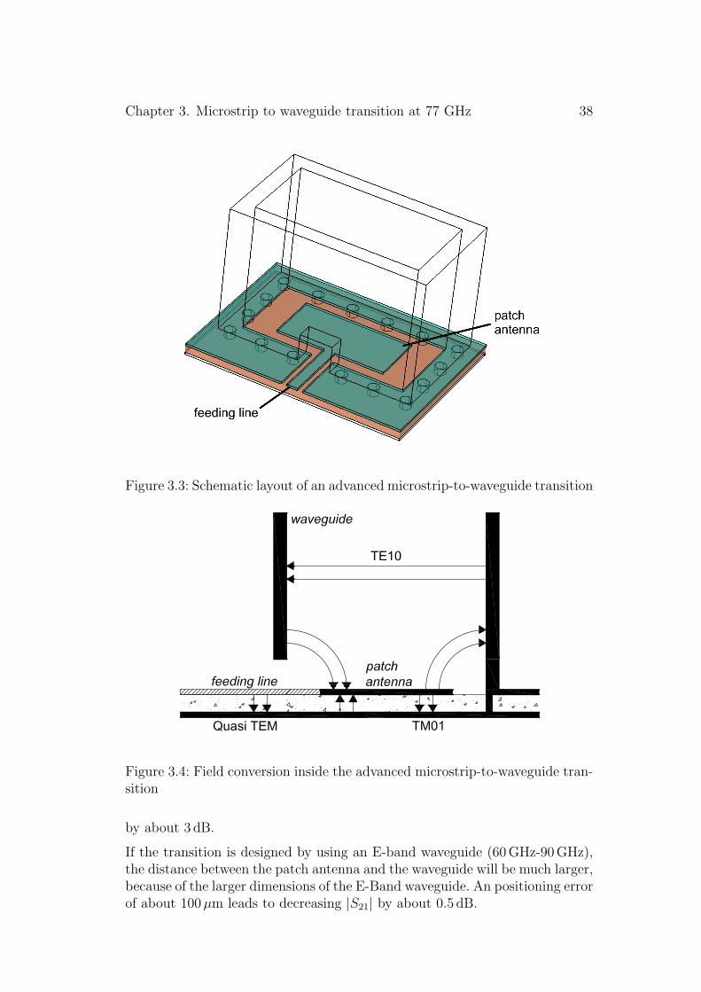
Another interesting microstrip-to-waveguide transition is shown in Fig. 3.1[Nihad Dib 97]. Here a waveguide is mounted directly on the microwave sub-strate and the field conversion is done inside the microwave substrate (seeFig. 3.2). The antenna is formed by a microstrip patch antenna with a ca-pacitive coupling, as shown in [Ramesh Garg 01]. The wavelength inside themicrowave substrate is shorter than inside the waveguide. In Fig. 3.2 the fieldcomes from the waveguide and is split by the patch antenna into two parts.The right part of the field is turned into the microwave substrate and becauseof ~S = ~E × ~H it is moving toward the microstrip. The left part of the fieldalso turns into the microwave substrate and because of ~S = ~E × ~H it is alsomoving toward the microstrip. If the length of the patch antenna is λ/2 insidethe microwave substrate, then these two parts will be added inphase.
35

Chapter 3. Microstrip to waveguide transition at 77 GHz 36
Figure 3.1: Schematic layout of a state-of-the-art microstrip-to-waveguide tran-sition
Figure 3.2: Field conversion of the state-of-the-art microstrip-to-waveguidetransition from Fig. 3.1
Chapter 3. Microstrip to waveguide transition at 77 GHz 37
3.2 Advanced design of a microstrip to waveguide
transition
The disadvantage of the design from Fig. 3.1 is that it can not be mounteddirectly on a metal block. It needs a metal layer with the microstrip on thebackside of the microwave substrate. We want to mount the waveguide directlyon a block of metal. Therefore we need a continuous ground plane on thebackside of the microwave substrate.
One possibility is to add another metal layer to the microwave substrate. Thedisadvantage is that we need 3 metal layers. Such a microwave substrate ismuch more expensive then a microwave substrate with two metal layers. Ad-ditionally the microstrip is not on the same layer like the matching element.Therefore we also have larger errors because of the tolerances of the produc-tion. These two layers have position errors and also the position errors of thedrilled holes can not be compensated easily.
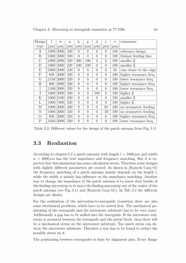
We need a microstrip-to-waveguide transition using a microwave substrate withonly two metal layers (one etched metal layer for the feeding line and matchingelement and one metal layer for the ground plane). A patch antenna, whichneeds only one etched metal layer (and a ground layer) is shown in Fig. 3.11(see [Ramesh Garg 01]). A transition using this patch antenna can be mounteddirectly on a block of metal and it is also much cheaper. Another advantageis that there are much less position errors. There is only one etched metallayer, therefore there is no position error between different layers. There arealso position errors of the drilled holes. If there is no metal layer inside themicrowave substrate, it can be drilled first and then the metal can be etchedaccording to the position of the drilled holes. This also leads to a lower positionerror.
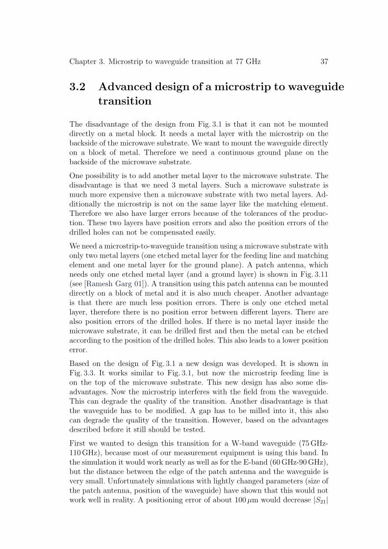
Based on the design of Fig. 3.1 a new design was developed. It is shown inFig. 3.3. It works similar to Fig. 3.1, but now the microstrip feeding line ison the top of the microwave substrate. This new design has also some dis-advantages. Now the microstrip interferes with the field from the waveguide.This can degrade the quality of the transition. Another disadvantage is thatthe waveguide has to be modified. A gap has to be milled into it, this alsocan degrade the quality of the transition. However, based on the advantagesdescribed before it still should be tested.
First we wanted to design this transition for a W-band waveguide (75GHz-110GHz), because most of our measurement equipment is using this band. Inthe simulation it would work nearly as well as for the E-band (60GHz-90GHz),but the distance between the edge of the patch antenna and the waveguide isvery small. Unfortunately simulations with lightly changed parameters (size ofthe patch antenna, position of the waveguide) have shown that this would notwork well in reality. A positioning error of about 100µm would decrease |S21|
Chapter 3. Microstrip to waveguide transition at 77 GHz 38
Figure 3.3: Schematic layout of an advanced microstrip-to-waveguide transition
Figure 3.4: Field conversion inside the advanced microstrip-to-waveguide tran-sition
by about 3 dB.
If the transition is designed by using an E-band waveguide (60GHz-90GHz),the distance between the patch antenna and the waveguide will be much larger,because of the larger dimensions of the E-Band waveguide. An positioning errorof about 100µm leads to decreasing |S21| by about 0.5 dB.
Chapter 3. Microstrip to waveguide transition at 77 GHz 39
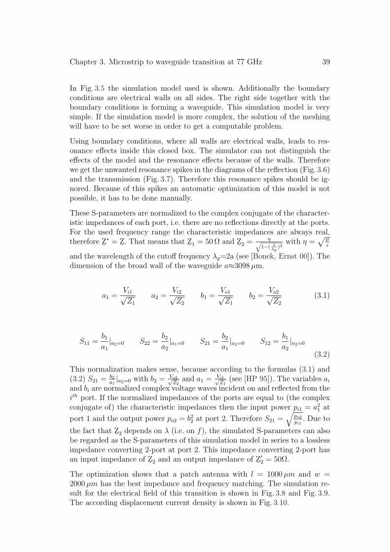
In Fig. 3.5 the simulation model used is shown. Additionally the boundaryconditions are electrical walls on all sides. The right side together with theboundary conditions is forming a waveguide. This simulation model is verysimple. If the simulation model is more complex, the solution of the meshingwill have to be set worse in order to get a computable problem.
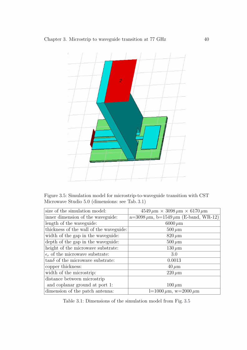
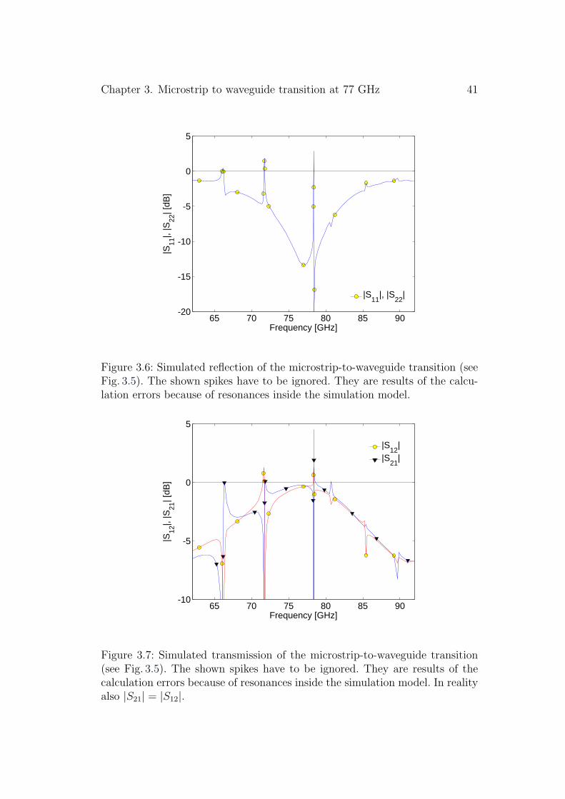
Using boundary conditions, where all walls are electrical walls, leads to res-onance effects inside this closed box. The simulator can not distinguish theeffects of the model and the resonance effects because of the walls. Thereforewe get the unwanted resonance spikes in the diagrams of the reflection (Fig. 3.6)and the transmission (Fig. 3.7). Therefore this resonance spikes should be ig-nored. Because of this spikes an automatic optimization of this model is notpossible, it has to be done manually.
These S-parameters are normalized to the complex conjugate of the character-istic impedances of each port, i.e. there are no reflections directly at the ports.For the used frequency range the characteristic impedances are always real,therefore Z
¯∗ = Z
¯. That means that Z
¯1 = 50 Ω and Z¯2 = ηq
1−( λλg
)2with η =
√µε
and the wavelength of the cutoff frequency λg=2a (see [Bonek, Ernst 00]). Thedimension of the broad wall of the waveguide a≈3098µm.
a1 =Vi1√Z1
a2 =Vi2√Z2
b1 =Vo1√Z1
b2 =Vo2√Z2
(3.1)
S11 =b1
a1
|a2=0 S22 =b2
a2
|a1=0 S21 =b2
a1
|a2=0 S12 =b1
a2
|a2=0
(3.2)
This normalization makes sense, because according to the formulas (3.1) and(3.2) S21 = b2
a1|a2=0 with b2 = Vo2√
Z2and a1 = Vi1√
Z1(see [HP 95]). The variables ai
and bi are normalized complex voltage waves incident on and reflected from theith port. If the normalized impedances of the ports are equal to (the complexconjugate of) the characteristic impedances then the input power pi1 = a2
1 at
port 1 and the output power po2 = b22 at port 2. Therefore S21 =
√po2
pi1. Due to
the fact that Z¯2 depends on λ (i.e. on f), the simulated S-parameters can also
be regarded as the S-parameters of this simulation model in series to a losslessimpedance converting 2-port at port 2. This impedance converting 2-port hasan input impedance of Z
¯2 and an output impedance of Z¯′2 = 50Ω.
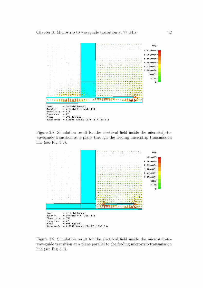
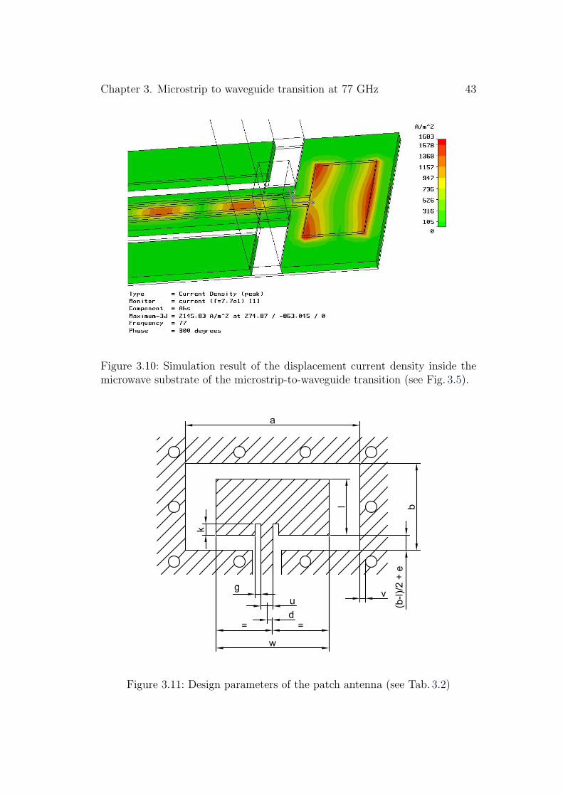
The optimization shows that a patch antenna with l = 1000 µm and w =2000 µm has the best impedance and frequency matching. The simulation re-sult for the electrical field of this transition is shown in Fig. 3.8 and Fig. 3.9.The according displacement current density is shown in Fig. 3.10.
Chapter 3. Microstrip to waveguide transition at 77 GHz 40
Figure 3.5: Simulation model for microstrip-to-waveguide transition with CSTMicrowave Studio 5.0 (dimensions: see Tab. 3.1)
size of the simulation model: 4549µm × 3098µm × 6170µminner dimension of the waveguide: a=3098µm, b=1549µm (E-band, WR-12)length of the waveguide: 6000µmthickness of the wall of the waveguide: 500µmwidth of the gap in the waveguide: 820µmdepth of the gap in the waveguide: 500µmheight of the microwave substrate: 130µmεr of the microwave substrate: 3.0tanδ of the microwave substrate: 0.0013copper thickness: 40µmwidth of the microstrip: 220µmdistance between microstripand coplanar ground at port 1: 100µm
dimension of the patch antenna: l=1000µm, w=2000µm
Table 3.1: Dimensions of the simulation model from Fig. 3.5
Chapter 3. Microstrip to waveguide transition at 77 GHz 41
65 70 75 80 85 90-20
-15
-10
-5
0
5
Frequency [GHz]
|S11
|, |S
22| [
dB]
|S11|, |S22|
Figure 3.6: Simulated reflection of the microstrip-to-waveguide transition (seeFig. 3.5). The shown spikes have to be ignored. They are results of the calcu-lation errors because of resonances inside the simulation model.
65 70 75 80 85 90-10
-5
0
5
Frequency [GHz]
|S12
|, |S
21| [
dB]
|S12||S21|
Figure 3.7: Simulated transmission of the microstrip-to-waveguide transition(see Fig. 3.5). The shown spikes have to be ignored. They are results of thecalculation errors because of resonances inside the simulation model. In realityalso |S21| = |S12|.
Chapter 3. Microstrip to waveguide transition at 77 GHz 42
Figure 3.8: Simulation result for the electrical field inside the microstrip-to-waveguide transition at a plane through the feeding microstrip transmissionline (see Fig. 3.5).
Figure 3.9: Simulation result for the electrical field inside the microstrip-to-waveguide transition at a plane parallel to the feeding microstrip transmissionline (see Fig. 3.5).
Chapter 3. Microstrip to waveguide transition at 77 GHz 43
Figure 3.10: Simulation result of the displacement current density inside themicrowave substrate of the microstrip-to-waveguide transition (see Fig. 3.5).
Figure 3.11: Design parameters of the patch antenna (see Tab. 3.2)
Chapter 3. Microstrip to waveguide transition at 77 GHz 44
Design l w u k g d e v commentstype [µm] [µm] [µm] [µm] [µm] [µm] [µm] [µm]
A 1000 2000 220 0 0 0 0 100 reference designB 1000 2000 100 0 0 0 0 100 thinner feeding lineC 1000 2000 220 200 100 0 0 100 smaller Z
¯D 1000 2000 220 100 100 0 0 100 smaller Z
¯E 1000 2000 220 0 0 0 0 50 vias closer to the edgeF 850 2000 220 0 0 0 0 100 higher resonance freq.G 1150 2000 220 0 0 0 0 100 lower resonance freq.H 900 2000 220 0 0 0 0 100 higher resonance freq.I 1100 2000 220 0 0 0 0 100 lower resonance freq.J 1000 2000 220 0 0 100 0 100 higher Z
¯K 1000 2100 220 0 0 0 0 100 smaller Z
¯L 1000 1900 220 0 0 0 0 100 higher Z
¯M 1000 2000 220 0 0 0 50 100 no symmetric feedingN 1000 2000 220 0 0 0 -50 100 no symmetric feedingO 950 2000 220 0 0 0 0 100 higher resonance freq.P 1050 2000 220 0 0 0 0 100 lower resonance freq.
Table 3.2: Different values for the design of the patch antenna from Fig. 3.11
3.3 Realization
According to chapter 3.2 a patch antenna with length l = 1000 µm and widthw = 2000 µm has the best impedance and frequency matching. But it is ex-pected that this simulation has some calculation errors. Therefore some designswith slightly different parameters are created. As shown in [Ramesh Garg 01]the frequency matching of a patch antenna mainly depends on the length l,while the width w mainly has influence on the impedance matching. Anotherway to change the impedance of the patch antenna is to insert slots beside ofthe feeding microstrip or to move the feeding microstrip out of the center of thepatch antenna (see Fig. 3.11 and [Ramesh Garg 01]). In Tab. 3.2 the differentdesigns are shown.
For the realization of the microstrip-to-waveguide transition there are alsosome mechanical problems, which have to be solved first. The mechanical po-sitioning of the waveguide and the microwave substrate has to be very exact.Additionally a gap has to be milled into the waveguide. If the microwave sub-strate is mounted between the waveguide and the metal block, then there willbe a mechanical stress on the microwave substrate. Too much stress can de-stroy the microwave substrate. Therefore a way has to be found to reduce thepossible stress on it.
The positioning between waveguides is done by alignment pins. Every flange

Chapter 3. Microstrip to waveguide transition at 77 GHz 45
Figure 3.12: ”Anti-cocking” flange of the waveguide before modification[Flann 05]. This flange is compatible with the standard UG385/U style flange,but has an additional outer ring to avoid cocking.
has two pins and two holes, therefore the connection is positioned by fouralignment pins (see Fig. 3.12). Two alignment pins should also be enough fora good positioning. In this way only the alignment pins of the waveguide areused and no alignment pins out of the microwave substrate are necessary.
For the assembly there also have to be assembling holes in the microwavesubstrate. As we can see in Fig. 1.25 inside a via there are always some tropesof copper. Also the width of the copper can change inside the via. In order toget lower tolerances the alignment hole should be copper-free. This is done bycovering the alignment holes before the epitaxial growth of copper for the viageneration.
The microwave substrate is very thin, therefore the alignment holes can easilybe damaged by mechanical stress from the waveguide. In order to avoid this,the alignment holes also have to be drilled into the metal block under themicrowave substrate. (see Fig. B.3)
For this board the production processes have to be modified a little bit (seeFig. 3.13). Normally the metal layers are etched before the vias are drilledinto it. Here the holes have to be drilled first. Then the layout for etching ispositioned according to the drilled holes. This results in position tolerances ofthe holes reduced to 50µm instead of 100µm. In order to avoid copper insidethe alignment holes, the according holes have to be covered during the viageneration. This cover is removed afterwards.
The manufacturer Elekonta Marek (see Chapter 1.7) has forgotten to coverthe alignment holes. Therefore I had to remove the copper tropes out of thehole by hand with a drill.
The waveguide has to be modified. A gap has to be milled into it as shown in

Chapter 3. Microstrip to waveguide transition at 77 GHz 46
Figure 3.13: Production processes for the microstrip-to-waveguide test-board
Figure 3.14: Photo of the modified waveguide flange
Fig. 3.14 and Fig. B.2. Since only the two alignment pins of the waveguide areused, there is enough space to mill a gap into the waveguide. The alignmentholes of the waveguide are not used.
In order to avoid too much mechanical stress on the microwave substrate, dis-tance shims are used. In Fig. 3.15 the assembly is shown before the waveguide

Chapter 3. Microstrip to waveguide transition at 77 GHz 47
Figure 3.15: Photo of the microstrip-to-waveguide transition board togetherwith the shims
is mounted. Therefore ”Anti-Cocking” flanges are used, as shown in Fig. 3.12.The outer ring of the flange is pressed onto the shims. Normal flanges do nothave this ring.
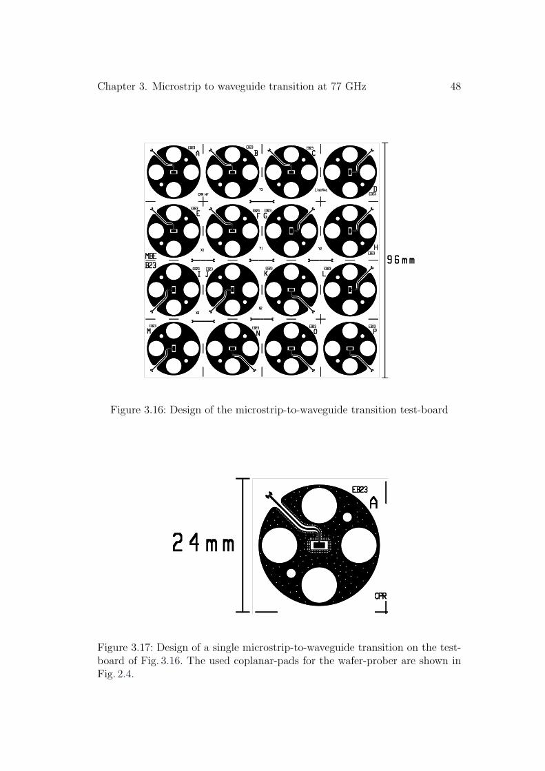
The according layout of the test-board can be seen in Fig. 3.16 and in detailin Fig. 3.17.A photo of the assembled design during the measurement can be seen inFig. 3.18. Originally also a design for a two-port measurement of a microstrip-to-waveguide-to-microstrip transition was created (see Fig. 3.19 and Fig. B.6).It would be possible to use this design for characterizing S21 of the transition.In principle the wafer probes can be mounted, but the according microscopeis unable to be driven so far to observe the coplanar pads of both ports. With-out microscope it is not possible to place the wafer-probes without damagingthem.
Chapter 3. Microstrip to waveguide transition at 77 GHz 48
Figure 3.16: Design of the microstrip-to-waveguide transition test-board
Figure 3.17: Design of a single microstrip-to-waveguide transition on the test-board of Fig. 3.16. The used coplanar-pads for the wafer-prober are shown inFig. 2.4.

Chapter 3. Microstrip to waveguide transition at 77 GHz 49
Figure 3.18: Photo of the 1-port measurement design of the advancedmicrostrip-to-waveguide transition together with the wafer probes
Figure 3.19: Photo of the 2-port measurement design of the advancedmicrostrip-to-waveguide transition

Chapter 3. Microstrip to waveguide transition at 77 GHz 50
3.4 Measurement results
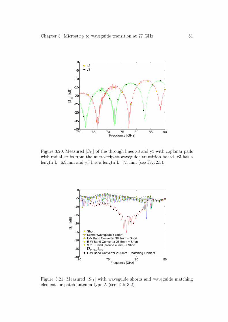
While no 2-port measurement was possible, the whole characterization has tobe done by a 1-port measurement. But the coplanar pads for the wafer-probesare a discontinuity. There will be reflections from the coplanar pads and fromthe patch antenna. These reflections will be either additive or subtractive.Additionally there are also losses on the transmission line to the patch antenna.
The solution is to measure different times with different terminations. Firstthe waveguide is terminated by a matching element. Then the waveguide isterminated with shorts in different distances. From the reflection with theshort we can determine the losses of the transmission. These reflections willbe sometimes additive and sometimes subtractive with the reflections of thepatch antenna and the contact-pad. Different lengths for the waveguide shortare used, therefore the maximum reflected energy can be seen. Finally themicrostrip-to-waveguide transition is terminated by a matching element. Nowthe energy transmitted by the transition is not reflected. Out of these resultsthe transmission can be estimated.
One should keep in mind that the contact pads are a discontinuity and so thereis also a reflection (shown in Fig. 2.11). Therefore it is not possible to analyze a|S11| < |S11,pads|. The reflection from though lines with coplanar pads from thesame board are shown in Fig. 3.20 for comparison. Because of a bad simulationmodel they have the smallest |S11| at about 50-55GHz.
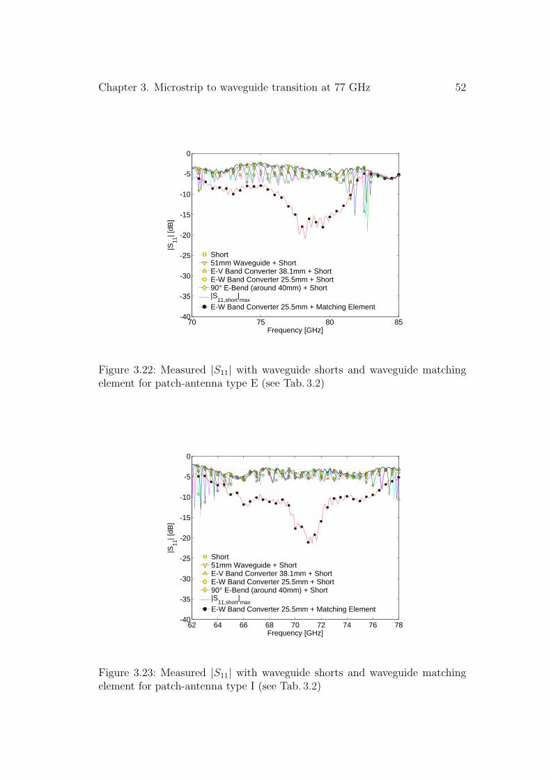
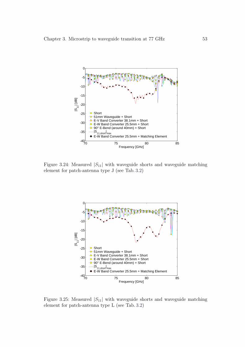
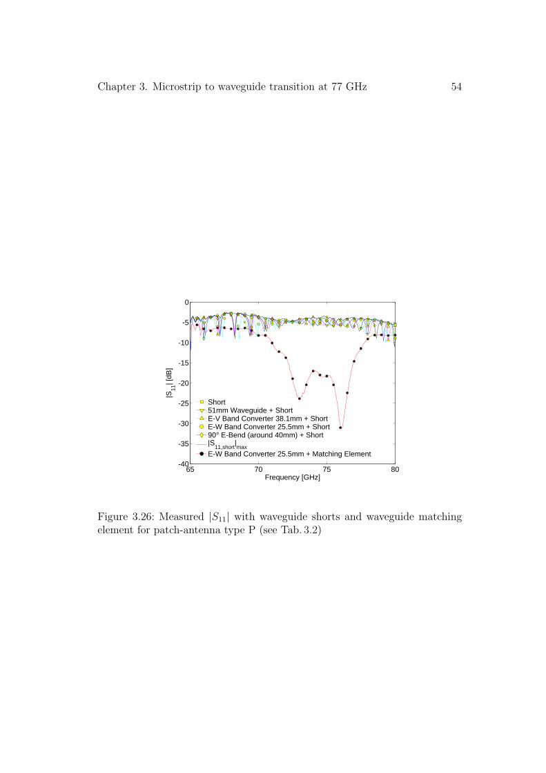
The measurement results for the designs A, E, I, J, L and P are the best,because they have the smallest |S11| (design parameters: see Tab. 3.2 andFig. 3.11). These results are shown in Fig. 3.21, Fig. 3.22, Fig. 3.23, Fig. 3.24,Fig. 3.25 and Fig. 3.26.
Chapter 3. Microstrip to waveguide transition at 77 GHz 51
60 65 70 75 80 85 90-40
-35
-30
-25
-20
-15
-10
-5
0
Frequency [GHz]
|S11
| [dB
]x3y3
Figure 3.20: Measured |S11| of the through lines x3 and y3 with coplanar padswith radial stubs from the microstrip-to-waveguide transition board. x3 has alength L=6.9mm and y3 has a length L=7.5mm (see Fig. 2.5).
70 75 80 85-40
-35
-30
-25
-20
-15
-10
-5
0
Frequency [GHz]
|S11
| [dB
]
Short51mm Waveguide + ShortE-V Band Converter 38.1mm + ShortE-W Band Converter 25.5mm + Short90° E-Bend (around 40mm) + Short|S11,short|maxE-W Band Converter 25.5mm + Matching Element
Figure 3.21: Measured |S11| with waveguide shorts and waveguide matchingelement for patch-antenna type A (see Tab. 3.2)
Chapter 3. Microstrip to waveguide transition at 77 GHz 52
70 75 80 85-40
-35
-30
-25
-20
-15
-10
-5
0
Frequency [GHz]
|S11
| [dB
]
Short51mm Waveguide + ShortE-V Band Converter 38.1mm + ShortE-W Band Converter 25.5mm + Short90° E-Bend (around 40mm) + Short|S11,short|maxE-W Band Converter 25.5mm + Matching Element
Figure 3.22: Measured |S11| with waveguide shorts and waveguide matchingelement for patch-antenna type E (see Tab. 3.2)
62 64 66 68 70 72 74 76 78-40
-35
-30
-25
-20
-15
-10
-5
0
Frequency [GHz]
|S11
| [dB
]
Short51mm Waveguide + ShortE-V Band Converter 38.1mm + ShortE-W Band Converter 25.5mm + Short90° E-Bend (around 40mm) + Short|S11,short|maxE-W Band Converter 25.5mm + Matching Element
Figure 3.23: Measured |S11| with waveguide shorts and waveguide matchingelement for patch-antenna type I (see Tab. 3.2)
Chapter 3. Microstrip to waveguide transition at 77 GHz 53
70 75 80 85-40
-35
-30
-25
-20
-15
-10
-5
0
Frequency [GHz]
|S11
| [dB
]
Short51mm Waveguide + ShortE-V Band Converter 38.1mm + ShortE-W Band Converter 25.5mm + Short90° E-Bend (around 40mm) + Short|S11,short|maxE-W Band Converter 25.5mm + Matching Element
Figure 3.24: Measured |S11| with waveguide shorts and waveguide matchingelement for patch-antenna type J (see Tab. 3.2)
70 75 80 85-40
-35
-30
-25
-20
-15
-10
-5
0
Frequency [GHz]
|S11
| [dB
]
Short51mm Waveguide + ShortE-V Band Converter 38.1mm + ShortE-W Band Converter 25.5mm + Short90° E-Bend (around 40mm) + Short|S11,short|maxE-W Band Converter 25.5mm + Matching Element
Figure 3.25: Measured |S11| with waveguide shorts and waveguide matchingelement for patch-antenna type L (see Tab. 3.2)
Chapter 3. Microstrip to waveguide transition at 77 GHz 54
65 70 75 80-40
-35
-30
-25
-20
-15
-10
-5
0
Frequency [GHz]
|S11
| [dB
]
Short51mm Waveguide + ShortE-V Band Converter 38.1mm + ShortE-W Band Converter 25.5mm + Short90° E-Bend (around 40mm) + Short|S11,short|maxE-W Band Converter 25.5mm + Matching Element
Figure 3.26: Measured |S11| with waveguide shorts and waveguide matchingelement for patch-antenna type P (see Tab. 3.2)
Conclusion
This master thesis was done at INFINEON Technologies AG, Corporate Re-search, Department for High Frequency Circuits (CPR HF), Munich. Currentlyfor on-board measurements SMA-connectors are used there. In this masterthesis alternative possibilities for on-board measurements were verified. A newmicrowave substrate was characterized up to 90GHz and 3 types of transitionsto microstrip transmission lines have been tested.
The microwave substrate Rogers RO3003-130µm tested seems to be goodenough for measurements up to 90GHz, although it is only recommended upto 40GHz. The losses are about 1 dB/cm at 50GHz and about 1.3 dB/cm at90GHz.
A transition from a microstrip transmission line to a coplanar V-ConnectorsV115FCPW 2.4mm coaxial from Anritsu was designed and tested. These con-nectors lead to losses of about 0.2 dB/connector. Nevertheless the mechanicaltolerances of the according board are still an unsolved issue (see Chapter 1.7).Maybe the board can be cut by laser to decrease the tolerances. Another pos-sibility would be to use a second microwave substrate on the bottom side forstrengthening. Then the microwave substrate would be harder and the mi-crostrip would not break easily during cutting.
For on-board measurements using the wafer-prober two different designs ofcoplanar pads have been developed. One design is using vias for the groundlines. This design can be used up to about 30GHz. The second design wasdeveloped using radial stubs. These stubs have been designed for 77GHz, butthe simulation model was not good enough, therefore the stubs used have theiroptimum frequency at about 50-55GHz. Stubs for 77GHz have been redesignedusing another simulation program.
The microstrip-to-waveguide transition could only be specified by a 1-portmeasurement. The radial stubs used for the wafer-prober have their optimumfrequency at about 50-55GHz, while the transition is optimized at 77GHz.The measured |S11| at 77GHz of this transition terminated with a matchingelement is ≤-15 dB, while the according losses are about 3-4 dB. Maybe |S11| ismuch less, but for a better specification the redesigned stubs for 77GHz have tobe used. Maybe another wafer-prober can be used for a 2-port characterization.
55

Appendix A
Verification of the substratematter constants
Straight Resonator
For the measurement of εeff and Q the method of the straight resonator[Hoffmann 83] is used. Here a straight resonator is built by a microstrip ofthe length n·λ/2. This resonator is coupled via two interaction gaps of thelength s. However the field at the end of a microstrip is very inhomogeneous.That means that the microstrip acts like an ideal microstrip with the additionallength ∆l. So this effect has to be taken into consideration for the calculationof the length of the microstrip-resonator.
The use of 2 microstrips with different lengths (l1 and l2 = 2·l1) has the ad-vantage, that this unwanted constant ∆l can be eliminated from the formulas.For a higher precision the resonance frequencies of these two resonators shouldbe nearly the same, but an estimation of ∆l is good enough.
As shown in [Hammerstad 81] the additional effective length ∆l can be esti-
Figure A.1: Undercutting of the test-board for the Anritsu V-connectors andwafer-prober measurements from Fig. 1.3
56
Chapter A. Substrate matter constants 57
mated by
∆l
h= 0.102·w/h + 0.106
w/h + 0.264·[1.166 +
εr + 1
εr
· (0.9 + ln(w/h + 2.475))
](A.1)
with an error of less than 1.7%. According to this formula a ∆l of about 55µmcan be estimated. Additionally we have to expect undercutting (see Fig. A.1).If we have an undercutting of ∆lUC then the additional effective length is∆l′ = ∆l − ∆lUC instead of ∆l. So a ∆l of 40µm was supposed. Anyhowthese effects have only a slight influence to the precision of the measurement,because in formula A.5 there is only the term l2 − l1, what means that ∆l iseliminated.
Determination of εr,eff and εr
If we use only one resonator εr,eff can be calculated at the resonance frequencyfRn by
εr,eff (fn) =
(nc0
2lfRn
)2
(A.2)
but ∆l can’t be compensated, therefore the errors of this measurement wouldbe too large.
If we take ∆l into consideration then we have to replace l by l + ∆l. If weuse 2 resonators with nearly the same resonance frequency, where the effectivelength l′2 = 2l′1 then we can compensate these errors.
l1 + 2∆l(1)n = n
λ(1)n
2=
nc0
2f(1)Rn ·√
εr,eff (f(1)Rn)
(A.3)
l2 + 2∆l(2)n = 2n
λ(2)n
2=
nc0
f(2)Rn
√εr,eff (f
(2)Rn)
(A.4)
Using A.3 and A.4 we come to the final formula
εr,eff (f(1)Rn) =
(nc0
2(l2 − l1)·2f
(1)Rn − f
(2)Rn
f(1)Rn ·f
(2)Rn
)2
. (A.5)
For the calculation of εr we have to take the dielectric filling factor qε intoaccount. By using εr,eff = 1+F
2εr + 1−F
2with F = 2·qε − 1 we get the formula
εr =2
1 + F
(εr,eff −
1− F
2
)(A.6)
Chapter A. Substrate matter constants 58
with the approximation for F:
F =1√
1 + 10 hw
(A.7)
In our case w = 300µm and h = 130µm, therefore F = 0.4330.
Determination of the Q-factor
In a similar way we also can calculate the Q-factor. QL is the loaded Q-factor.
QL(fRn) =fRn
2∆fn
=fRn
f(o)n − f
(u)n
(A.8)
Here fRn is the resonance frequency, while f(o)n and f
(u)n are the frequency
points, where |S21| is decreased by 3dB in comparison to fRn.
The unloaded Q can be calculated from QL with
Q(fRn) =QL(fRn)
1− |S21(fRn)|. (A.9)
Now Q can be compared with the Q-factor Qε caused by tanδε.
Qε =1
tanδε
·(
1 +1− F
εr(1 + F )
)(A.10)
F = 0.4330 (see (A.7) )
This leads to Qε=870. So the losses because of tanδε can be neglected. Themeasured Q is nearly proportional to
√f up to 50 GHz. This means that the
losses because of the skin effect are dominant. While the losses because of theskin effect are proportional to
√f , the length of the resonator is proportional
to 1f. Which means that the quality factor Qρ caused by the skin effect becomes
proportional to√
f .
Chapter A. Substrate matter constants 59
0 10 20 30 40 50-110
-100
-90
-80
-70
-60
-50
-40
-30
-20
Frequency [GHz]
|S21
| [dB
]
Resonator 1Resonator 2Resonator 3Resonator 4
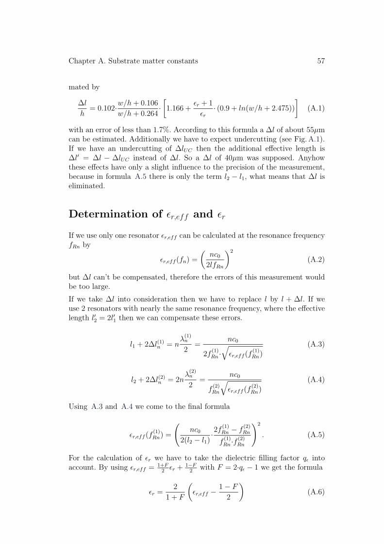
Figure A.2: Resonance frequencies at about 10, 20, 30, 40 and 50GHz
73 74 75 76 77 78 79 80-20
-18
-16
-14
-12
-10
Frequency [GHz]
|S21
| [dB
]
Resonator X1Resonator X2Resonator Y1Resonator Y2
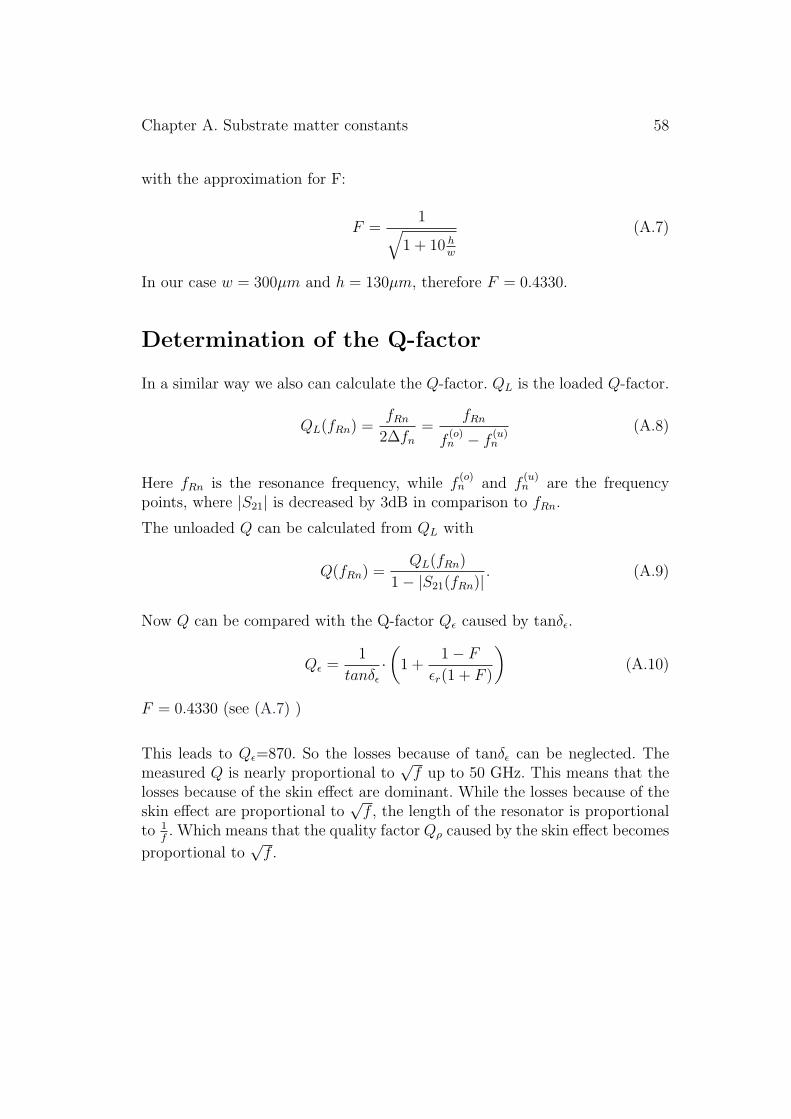
Figure A.3: Resonance frequencies at about 80GHz
Chapter A. Substrate matter constants 60
9.6 9.7 9.8 9.9 10 10.1
-60
-55
-50
-45
Frequency [GHz]
|S21
| [dB
]
Resonator 1Resonator 2
19.2 19.4 19.6 19.8 20 20.2-60
-55
-50
-45
-40
-35
Frequency [GHz]
|S21
| [dB
]
Resonator 1Resonator 2Resonator 3
(a) 10GHz (b) 20GHz
29.2 29.4 29.6 29.8 30
-45
-40
-35
-30
Frequency [GHz]
|S21
| [dB
]
Resonator 1Resonator 2
38 38.5 39 39.5 40
-40
-35
-30
-25
Frequency [GHz]
|S21
| [dB
]
Resonator 1Resonator 2Resonator 3Resonator 4
(c) 30GHz (d) 40GHz
48.5 49 49.5-40
-38
-36
-34
-32
-30
-28
Frequency [GHz]
|S21
| [dB
]
Resonator 1Resonator 2
(e) 50GHz
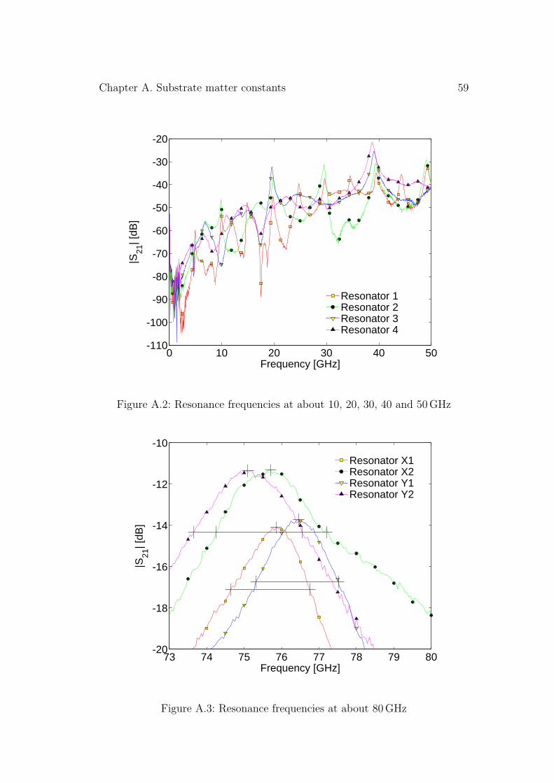
Table A.1: Resonance frequencies at about 10, 20, 30, 40 and 50GHz: detailsfrom Fig.A.2

Chapter A. Substrate matter constants 61
Resonators frequency n l1 l2 f(1)Rn f
(2)Rn εr,eff εr
[GHz] [µm] [µm] [GHz] [GHz] at f(1)Rn
2 and 1 ≈10 1 9520 19120 9.815 9.865 2.480 3.065
3 and 2 ≈20 1 4720 9520 19.580 19.745 2.459 3.0372 and 1 ≈20 2 9520 19120 19.745 19.745 2.501 3.096
2 and 1 ≈30 3 9520 19120 29.475 29.625 2.475 3.058
4 and 3 ≈40 1 2320 4720 38.70 39.11 2.497 3.0893 and 2 ≈40 2 4720 9520 39.11 39.365 2.484 3.0722 and 1 ≈40 4 9520 19120 39.365 39.45 2.496 3.087
2 and 1 ≈50 5 9520 19120 48.99 49.16 2.505 3.100
X2 and X1 ≈80 1 1120 2320 75.7 75.85 2.701 3.375Y2 and Y1 ≈80 1 1120 2320 75.2 76.45 2.582 3.208
Table A.2: Calculation of εr,eff and εr
Res. freq. n fRn f(u)n f
(o)n |S21|[dB] QL Q
[GHz] [GHz] [GHz] [GHz] at fRn
2 ≈10 1 9.815 9.6897 9.9175 -45.8 43 431 ≈10 2 9.865 9.7635 10.005 -52.2 41 41
3 ≈20 1 19.58 19.4101 19.7692 -32.4 55 562 ≈20 2 19.745 19.5695 19.998 -36.7 46 471 ≈20 4 19.745 19.5945 19.917 -45.7 61 62
2 ≈30 3 29.475 29.230 29.673 -31.1 67 681 ≈30 6 29.625 29.418 29.878 -37.6 64 65
4 ≈40 1 38.7 38.34 39.05 -24.0 55 583 ≈40 2 39.11 38.743 39.4345 -25.4 57 602 ≈40 4 39.365 39.103 39.655 -28.8 71 741 ≈40 8 39.45 39.185 39.79 -34.4 65 66
2 ≈50 5 48.99 48.705 49.32 -27.8 80 831 ≈50 10 49.16 48.92 49.53 -31.5 81 83
X1 ≈80 2 75.85 74.65 76.75 -14.1 36 45X2 ≈80 1 75.7 74.25 77.2 -11.3 26 35Y1 ≈80 2 76.45 75.32 77.52 -13.7 35 44Y2 ≈80 1 75.2 73.65 76.55 -11.3 26 36
Table A.3: Calculation of Q

Chapter A. Substrate matter constants 62
0 20 40 60 80
3
3.1
3.2
3.3
3.4
Frequency [GHz]
rel.
perm
eabi
lity ε r
measuredapproximated
Figure A.4: Measurement results for εr
0 20 40 60 802.4
2.5
2.6
2.7
Frequency [GHz]
rel.
eff.
perm
eabi
lity ε r,e
ff measuredapproximated
Figure A.5: Measurement results for εr,eff
0 20 40 60 800
20
40
60
80
Frequency [GHz]
Q-fa
ctor
measuredapproximated
Figure A.6: Measurement results for Q
Appendix B
Mechanical drawings
2.9
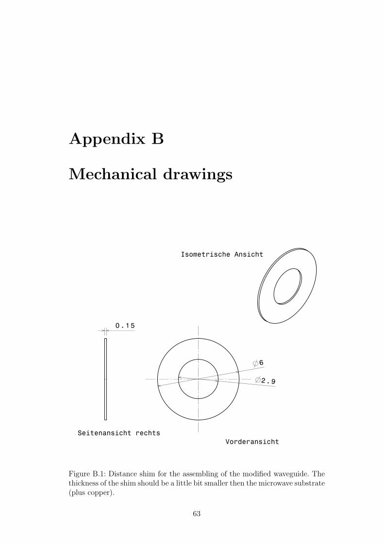
Figure B.1: Distance shim for the assembling of the modified waveguide. Thethickness of the shim should be a little bit smaller then the microwave substrate(plus copper).
63

Chapter B. Mechanical drawings 64
45
Figure B.2: Modified waveguide flange for a microstrip-to-waveguide transition
Chapter B. Mechanical drawings 65
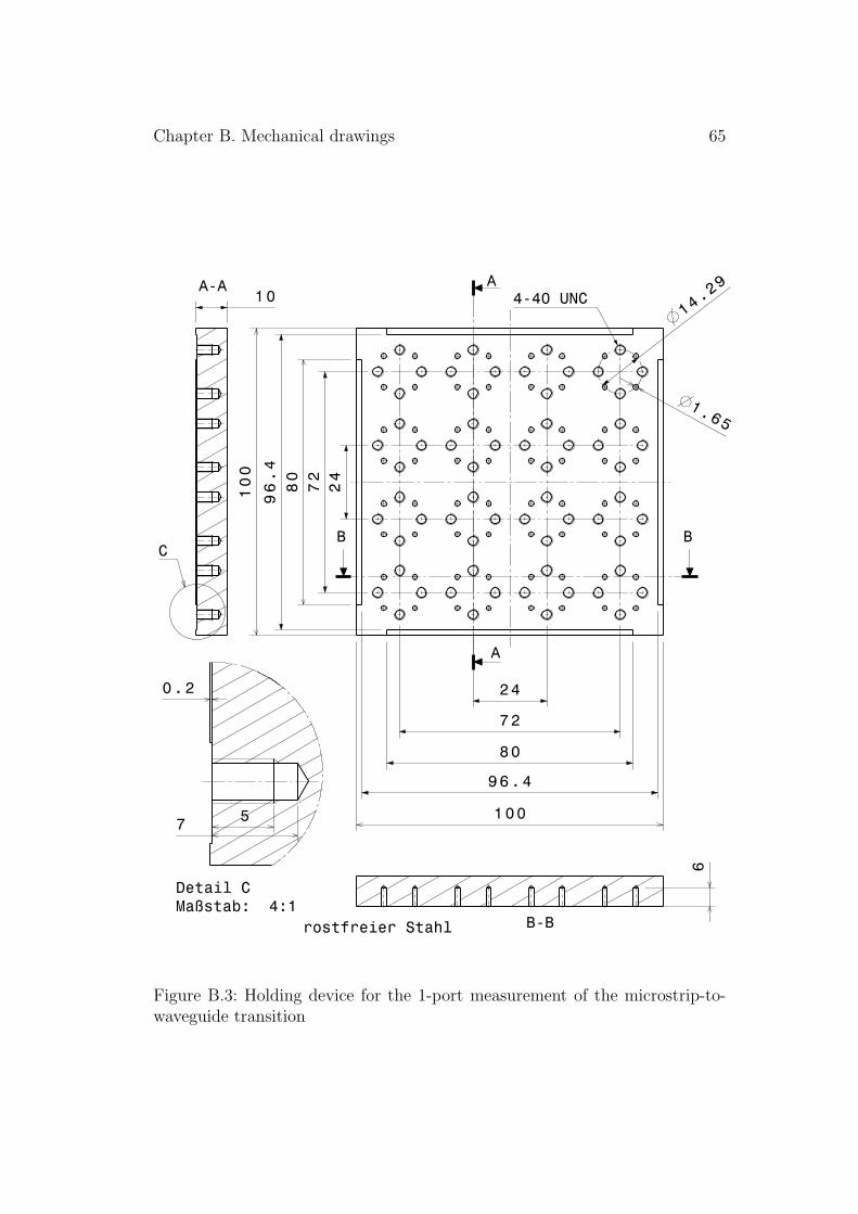
1.65
Figure B.3: Holding device for the 1-port measurement of the microstrip-to-waveguide transition

Chapter B. Mechanical drawings 66
3M
Figure B.4: Part 1 of the holding device for the 2-port measurement of themicrostrip-to-waveguide transition
Chapter B. Mechanical drawings 67
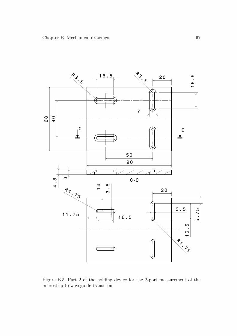
Figure B.5: Part 2 of the holding device for the 2-port measurement of themicrostrip-to-waveguide transition
Chapter B. Mechanical drawings 68
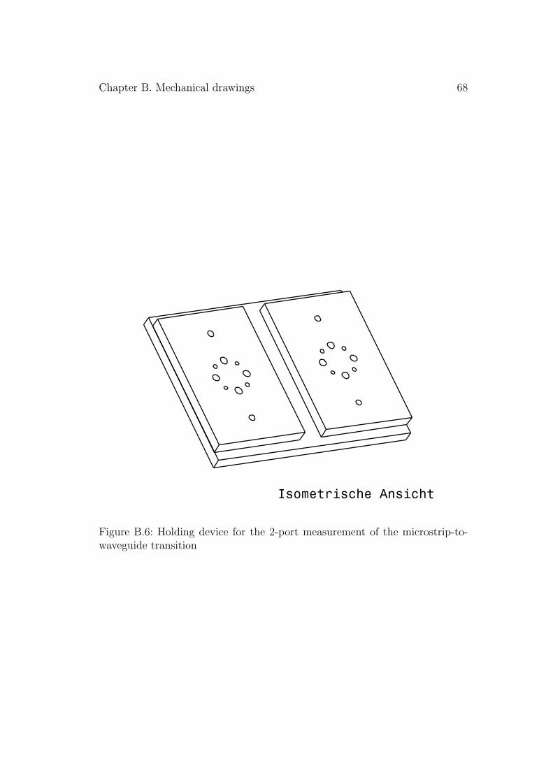
Figure B.6: Holding device for the 2-port measurement of the microstrip-to-waveguide transition
Chapter B. Mechanical drawings 69
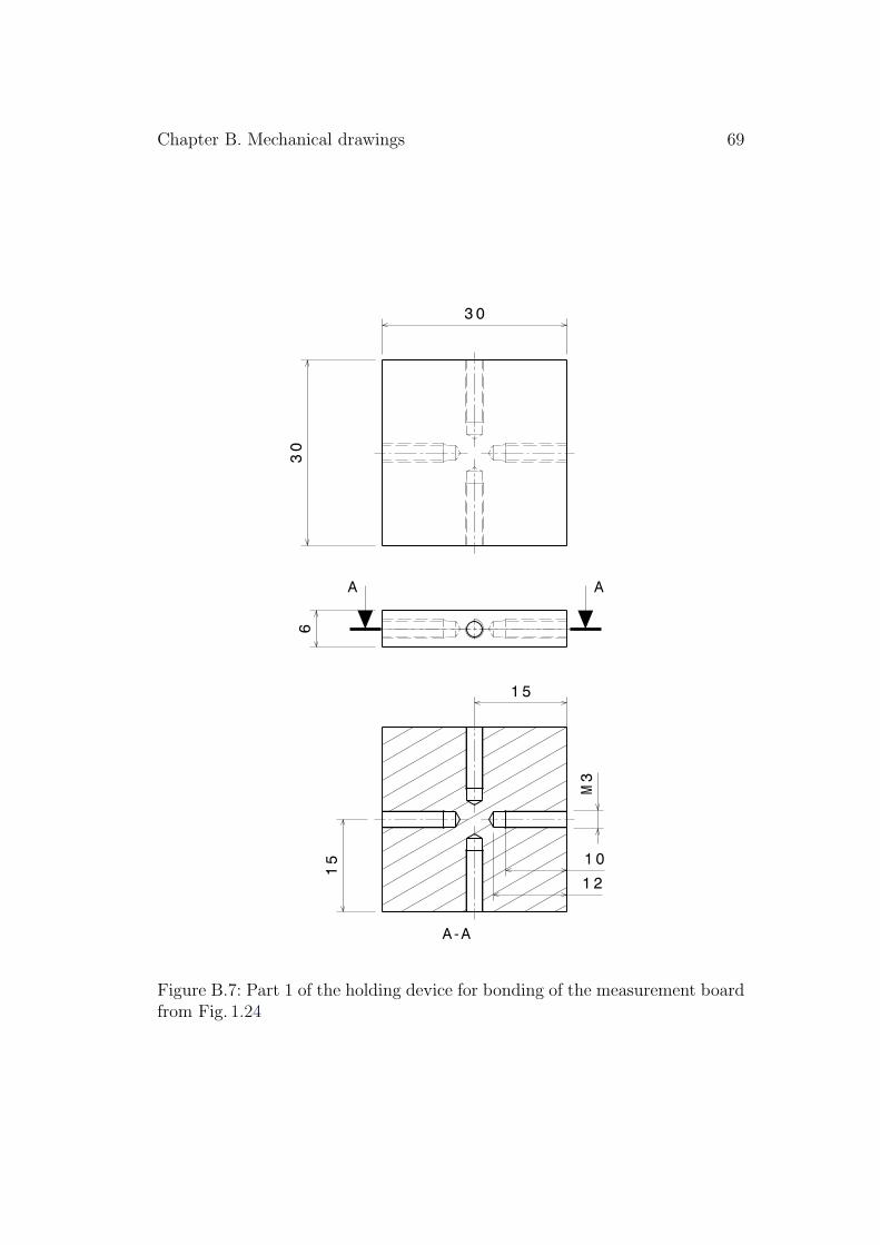
Figure B.7: Part 1 of the holding device for bonding of the measurement boardfrom Fig. 1.24
Chapter B. Mechanical drawings 70
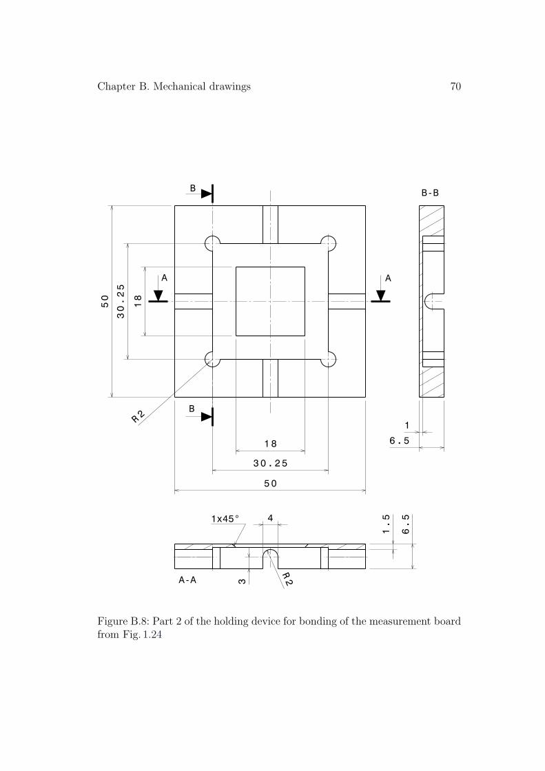
2R
2R
Figure B.8: Part 2 of the holding device for bonding of the measurement boardfrom Fig. 1.24

Acknowledgements
The work presented was supported by INFINEON Technologies AG, Corpo-rate Research, Department for High Frequency Circuits (CPR HF), Munich.
Special thanks to my colleague Dr.Werner Simburger for the initial ideas. Fur-ther, continuous support by Herbert Knapp and Klaus Aufinger is gratefullyacknowledged. My gratitude also goes to Guo Li for critical reading of themanuscript.
I would like to take this opportunity to thank my parents who helped me inany situation during my studies.
71

Bibliography
[Agilent 00] Agilent, “Agilent 8510-13, Measuring Noninsertable De-vices, Product Note”, http://www.agilent.com, 2000.
[Anritsu 01] Anritsu, “Three and Four Port S-Parameter Measurements,Application Note”, http://www.sss-mag.com/spara.html,November 2001.
[Bonek, Ernst 00] Bonek, Ernst, “Wellenausbreitung 1”, Script for the courseWellenausbreitung 1 at the Technical University of Vienna,October 2000.
[Flann 05] Flann, “FMI Catalogue - Microwave Products 2005”,http://www.flann.com, 2005.
[Hammerstad 81] E.O. Hammerstad, “Computer-Aided Design of MicrostripCouplers with Accurate Discontinuity Models”, Symposiumon Microwave Theory and Techniques, vol. , pp. 54–56, June1981.
[Hoffmann 83] Reinmut K. Hoffmann, Integrierte Mikrowellenschaltungen,Springer-Verlag, 1983.
[HP 95] HP, “S-Parameter Techniques for Faster, More AccurateNetwork Design, Test & Measurement, Application Note95-1”, 1995.
[Magerl 02] Gottfried Magerl, “Integrierte Mikrowellenmesstechnik”,Script for the course Integrierte Mikrowellenmesstechnik atthe Technical University of Vienna, LVA-Nr.: 381.002, Oc-tober 2002.
[Nihad Dib 97] Nihad Dib and Amjad Omar, “Analysis of Grounded Copla-nar Waveguide Fed Patches and Waveguides”, 1997.
[Pollendorfer 04] Christian Pollendorfer, “Characterization of a 17 GHzWLAN/ISM Receiver Frontend”, Master’s thesis, TechnicalUniversity of Vienna, September 2004.
72

73
[Ramesh Garg 01] Inder Bahl Ramesh Garg, Prakash Bhartia and Apisak It-tipiboon, Microstrip Antenna Design Handbook, ArtechHouse, 2001.
[Weiss 04] Franz Weiss, “Modeling of Monolithic Integrated Transmis-sion Lines”, Master’s thesis, Technical University of Vienna,September 2004.