Embed Size (px)
Citation preview
4Design Automation and Testing for FPGAs
Simulation
Test benchesThe overall goal of any hardware design is to ensure that thedesign meets the requirements of the design specification. Inorder to measure this is indeed the case we need to not only simu-late the design representation in a hardware description language(such as VHDL), but also to ensure that whatever tests we under-take are appropriate and demonstrate that the specification hasbeen met.
The way that designers can test their designs in a simulator is bycreating a ‘test bench’. This is directly analogous to a real experi-mental test bench in the sense that stimuli are defined, and theresponses of the circuit measured to ensure that they meet thespecification.
In practice, the test bench is simply a VHDL model that gener-ates the required stimuli and checks the responses. This can be insuch a way that the designer can view the waveforms and manu-ally check them, or by using VHDL constructs to check the designresponses automatically.
Test bench goalsThe goals of any test bench are twofold. The first is primarily toensure that correct operation is achieved. This is essentially a‘functional’ test. The second goal is to ensure that a synthesiseddesign still meets the specification (particularly with a view totiming errors).
Ch04-H6845.qxd 4/5/07 11:23 AM Page 30
Simple test bench: instantiating componentsConsider a simple combinatorial VHDL model given below:
library ieee;use ieee.std_logic_1164.all;entity cct is
port ( in0, in1 : in std_logic;out1 : out std_logic
);end;
architecture simple of cct isbegin
out1 <= in0 AND in1 ;end;
This simple model is clearly a two input AND gate, and to test theoperation of the component we need to do several things.
First, we must include the component in a new VHDL design. Sowe need to create a basic test bench. The listing below shows howa basic entity (with no connections) is created, and then the archi-tecture contains both the component declaration and the signals totest the design.
-- library declarationslibrary ieee;use ieee.std_logic_1164.all;
-- empty entity declarationentity test isend;
-- test bench architecturearchitecture testbench of test is
-- component declarationcomponent cct
port ( in0, in1 : in std_logic;out1 : out std_logic
);end component;-- test bench signal declarationssignal in0, in1, out1 : std_logic;
-- architecture bodyBegin
-- declare the Circuit Under Test (CUT)CUT : cct port map ( in0, in1, out1 );
end;
This test bench will compile in a VHDL simulator, but is not par-ticularly useful as there are no definitions of the input stimuli (sig-nals in0 and in1) that will exercise the Circuit Under Test (CUT).
Design Automation and Testing for FPGAs
31
Ch04-H6845.qxd 4/5/07 11:23 AM Page 31
Design Recipes for FPGAs
32
If we wish to add stimuli to our test bench we have some signif-icant advantages over our design VHDL – the most appealing isthat we generally don’t need to adhere to any design rules or evenmake the code synthesisable. Test bench code is generally designedto be ‘off chip’ and therefore we can make the code as abstract orbehavioral as we like and it will still be fit for purpose. We can usewait statements, file read and write, assertions and other non-synthesisable code options.
Adding stimuliIn order to add a basic set of stimuli to our test bench, we couldsimply define the values of the input signals in0 and in1 with asimple signal assignment:
beginCUT : cct port map ( in0, in1, out1 );
in0 <= ‘0’;in1 <= ‘1’;
end;
Clearly this is not very complex or dynamic test bench, so to add a sequence of events we can modify the signal assignments toinclude numerous value, time pairs defining a sequence of values.
beginCUT : cct port map ( in0, in1, out1 );
in0 <= ‘0’ after 0 ns, ‘1’ after 10 ns, ‘0’ after20 ns;
in1 <= ‘0’ after 0 ns, ‘1’ after 15 ns, ‘0’ after 25 ns;
end;
While this method is useful for small circuits, clearly for morecomplex realistic designs it is of limited value. Another approachis to define a constant array of values that allow a number of teststo be carried out with a relatively simple test bench and applying adifferent set of stimuli and responses in turn.
For example, we can exhaustively test our simple two input logicdesign using a set of data in a record. A VHDL record is simply acollection of types grouped together defined as a new type.
type testdata is recordin0 : std_logic;in1 : std_logic;
end;
Ch04-H6845.qxd 4/5/07 11:23 AM Page 32
Design Automation and Testing for FPGAs
33
With a new composite type, such as a record, we can then create anarray, just as in any standard VHDL type. This requires another typedeclaration, of the array type itself.
type data_array is array (natural range <>) of data_array
With these two new types we can simply declare a constant (oftype data_array) that is an array of record values (of type testdata)that fully describe the data set to be used to test the design. Noticethat the type data_array does not have a default range, but that thisis defined by the declaration in this particular test bench.
constant test_data : data_array := ( (‘0’, ‘0’), (‘0’,‘1’), (‘1’, ‘0’), (‘1’, ‘1’) );
The beauty of this approach is that we can change from a systemthat requires every test stimulus to be defined explicitly, to onewhere a generic test data process will read values from pre-defined arrays of data. In the simple test example presented here,an example process to apply each set of test data in turn could beimplemented as follows:
processbegin
for i in test_data’range loopin0 <= test_data(i).in0;in1 <= test_data(i).in1;wait for 100 ns;
end loopwait;
end process;
There are several interesting aspects to this piece of test benchVHDL. The first is that we can use behavioral VHDL (wait for100 ns) as we are not constrained to synthesize this to hardware.Secondly, by using the range operator, the test bench becomesunconstrained by the size of the data set. Finally, the individualrecord elements are accessed using the hierarchical constructtest_data(i).in0 or test_data(i).in1, respectively.
Libraries
IntroductionVHDL as a language on its own is actually very limited in thebreadth of the data types and primitive models available. As a result,libraries are required to facilitate design re-use and standard data
Ch04-H6845.qxd 4/5/07 11:23 AM Page 33
Design Recipes for FPGAs
34
types for model exchange, re-use and synthesis. The primarylibrary for standard VHDL design is the IEEE library. Within theIEEE Design Automation Standards Committee (DASC), variouscommittees have developed libraries, packages and extensions tostandard VHDL. Some of these are listed below:
• IEEE Std 1076 Standard VHDL Language
• IEEE Std 1076.1 Standard VHDL Analog and Mixed-SignalExtensions (VHDL-AMS)
• IEEE Std 1076.1.1 Standard VHDL Analog and Mixed-Signal Extensions – Packages for Multiple Energy DomainSupport
• IEEE Std 1076.4 Standard VITAL ASIC (ApplicationSpecific Integrated Circuit) Modeling Specification (VITAL)
• IEEE Std 1076.6 Standard for VHDL Register TransferLevel (RTL) Synthesis (SIWG)
• IEEE Std 1076.2 IEEE Standard VHDL MathematicalPackages (math)
• IEEE Std 1076.3 Standard VHDL Synthesis Packages (vhdlsynth)
• IEEE Std 1164 Standard Multivalue Logic System forVHDL Model Interoperability (Std_logic_1164)
Each of these ‘working groups’ are volunteers who come from acombination of academia, EDA industry and user communities,and collaborate to produce the IEEE Standards (usually revisedevery 4 years).
Using librariesIn order to use a library, first the library must be declared:
library ieee;
Within each library a number of VHDL packages are defined, thatallow specific data types or functions to be employed in the design.For example, in digital systems design, we require logic data types,and these are not defined in the basic VHDL standard (1076).Standard VHDL defines integer, boolean and bit types, but not astandard logic definition. This is obviously required for digitaldesign and an appropriate IEEE standard was developed for thispurpose – IEEE 1164. It is important to note that IEEE Std 1164 is
Ch04-H6845.qxd 4/5/07 11:23 AM Page 34
Design Automation and Testing for FPGAs
35
NOT a subset of VHDL (IEEE 1076), but is defined for hardwaredescription languages in general.
Std_logic librariesThere are a number of std_logic libraries available in the IEEElibrary and these are:
• std_logic_1164
• std_logic_arith
• std_logic_unsigned
• std_logic_signed
• std_logic_entities
• std_logic_components
• std_logic_misc
• std_logic_textio
In order to use a particular element of a package in a design, theuser is required to declare their use of a package using the USE com-mand. For example, to use the standard IEEE logic library, the useneeds to add a declaration after the library declaration as follows:
library ieee;use ieee.std_logic_1164.all;
The std_logic_1164 package is particularly important for mostdigital design, especially for Field Programmable Gate Array(FPGA), because it defines the standard logic types used by ALLthe commercially available simulation and synthesis software tools,and is included as a standard library. It incorporates not only thedefinition of the standard logic types, but also conversion functions(to and from the standard logic types) and also manages the conver-sion between signed, unsigned and logic array variables.
Std_logic type definitionAs it is such an important type, the std_logic type is described inthis section. The type has the following definition:
• ‘U’: uninitialized; this signal hasn’t been set yet
• ‘X’: unknown; impossible to determine this value/result
• ‘0’: logic 0
Ch04-H6845.qxd 4/5/07 11:23 AM Page 35
Design Recipes for FPGAs
36
• ‘1’: logic 1
• ‘Z’: High Impedance
• ‘W’: Weak signal, can’t tell if it should be 0 or 1
• ‘L’: Weak signal that should probably go to 0
• ‘H’: Weak signal that should probably go to 1
• ‘-’: Don’t care
These definitions allow resolution of logic signals in digitaldesigns in a standard manner that is predictable and repeatableacross software tools and platforms. The operations that can becarried out on the basic std_logic data types are the standard builtin VHDL logic functions:
• and
• nand
• or
• nor
• xor
• xnor
• not
An example of the use of the std_logic library would be to definea simple logic gate – in this case a three input nand gate:
library ieee;use ieee.std_logic_1164.all;
entity nand3 isport ( in0, in1, in2 : in std_logic;
out1 : out std_logic ) ;end;
architecture simple of nand3 isbegin
out1 <= in0 nand in1 nand in2;end;
Synthesis
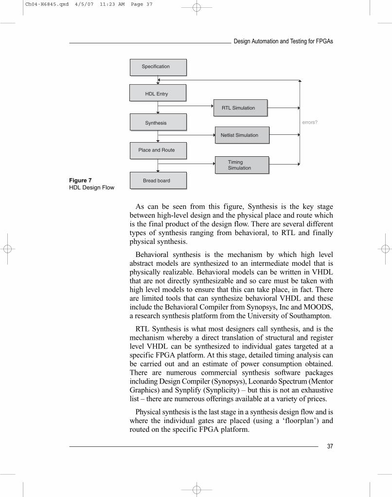
Design flow for synthesisThe basic HDL design flow is shown in Figure 7.
Ch04-H6845.qxd 4/5/07 11:23 AM Page 36
Design Automation and Testing for FPGAs
37
As can be seen from this figure, Synthesis is the key stagebetween high-level design and the physical place and route whichis the final product of the design flow. There are several differenttypes of synthesis ranging from behavioral, to RTL and finallyphysical synthesis.
Behavioral synthesis is the mechanism by which high levelabstract models are synthesized to an intermediate model that isphysically realizable. Behavioral models can be written in VHDLthat are not directly synthesizable and so care must be taken withhigh level models to ensure that this can take place, in fact. Thereare limited tools that can synthesize behavioral VHDL and theseinclude the Behavioral Compiler from Synopsys, Inc and MOODS,a research synthesis platform from the University of Southampton.
RTL Synthesis is what most designers call synthesis, and is themechanism whereby a direct translation of structural and registerlevel VHDL can be synthesized to individual gates targeted at a specific FPGA platform. At this stage, detailed timing analysis canbe carried out and an estimate of power consumption obtained.There are numerous commercial synthesis software packagesincluding Design Compiler (Synopsys), Leonardo Spectrum (MentorGraphics) and Synplify (Synplicity) – but this is not an exhaustivelist – there are numerous offerings available at a variety of prices.
Physical synthesis is the last stage in a synthesis design flow and iswhere the individual gates are placed (using a ‘floorplan’) androuted on the specific FPGA platform.
Specification
HDL Entry
Synthesis
Bread board
TimingSimulation
errors?
Place and Route
Netlist Simulation
RTL Simulation
Figure 7HDL Design Flow
Ch04-H6845.qxd 4/5/07 11:23 AM Page 37
Design Recipes for FPGAs
38
Synthesis issuesSynthesis basically transforms program-like VHDL into a truehardware design (netlist). It requires a set of inputs, a VHDLdescription, timing constraints (when outputs need to be ready,when inputs will be ready, data to estimate wire delay), a technol-ogy to map to (list of available blocks and their size/timing infor-mation) and information about design priorities (area vs. speed)
For big designs, the VHDL will typically be broken into modulesand then synthesized separately. 10 K gates per module was a rea-sonable size in the 1990s, however tools can handle a lot more now.
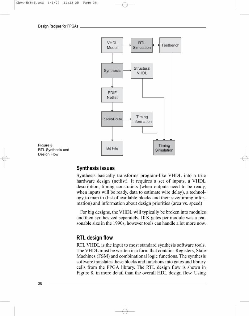
RTL design flowRTL VHDL is the input to most standard synthesis software tools.The VHDL must be written in a form that contains Registers, StateMachines (FSM) and combinational logic functions. The synthesissoftware translates these blocks and functions into gates and librarycells from the FPGA library. The RTL design flow is shown inFigure 8, in more detail than the overall HDL design flow. Using
VHDLModel
RTLSimulation
Testbench
Synthesis StructuralVHDL
EDIFNetlist
Place&Route
Bit File
TimingInformation
TimingSimulation
Figure 8RTL Synthesis andDesign Flow
Ch04-H6845.qxd 4/5/07 11:23 AM Page 38
Design Automation and Testing for FPGAs
39
RTL VHDL restricts the scope of the designer as it precludes algo-rithmic design – as we shall see later. This approach forces thedesigner to think at quite a low level – making the resulting codesometimes verbose and cumbersome. It also forces structuraldecisions early in the design process – restrictive and not alwaysadvisable, or helpful.
The Design process starts from RTL VHDL:
• Simulation (RTL) – is needed to develop a test bench(VHDL).
• Synthesis (RTL) – targeted at a standard FPGA platform.
• Timing simulation (Structural) – simulate to check timing.
• Place and route using standard tools (e.g. Xilinx DesignManager).
Although there are a variety of software tools available for synthe-sis (such as Leonardo Spectrum or Synplify), they all have gener-ally similar approaches and design flows.
Physical design flowSynthesis generates a netlist of devices plus interconnections. The‘place and route’ software figures out where the devices go andhow to connect them. The results not as good as you’d like; a 40 to60 per cent utilization of devices and wires is typical. The designercan trade off run time against greater utilization to some degree, butthere are serious limits. Typically the FPGA vendor will provide asoftware toolkit (such as the Xilinx Design Navigator or Altera’sQuartus tools) that manages the steps involved in physical design.
Regardless of the particular physical synthesis flow chosen, thesteps required to translate the VHDL or EDIF output from an RTLsynthesis software program into a physically downloadable bit fileare essentially the same and are listed below:
1. Translate
2. Map
3. Place
4. Route
5. Generate accurate timing models and reports
6. Create binary files for download to device
Ch04-H6845.qxd 4/5/07 11:23 AM Page 39

Design Recipes for FPGAs
40
Place and routeThere are two main techniques to place and route in current com-mercial software which are recursive cut and simulated annealing.
Recursive cutIn a recursive cut algorithm, we divide the netlist into two halves,move devices between halves to minimize the number of wiresthat cross cut (while keeping the number of devices in each halfthe same). This is repeated to get smaller and smaller blocks.
Timing analysisStatic timing analysis is the most commonly-used approach. Instatic timing analysis, we calculate the delay from each input toeach output of all devices. The delays are added up along each paththrough circuit to get the critical path through the design and hencethe fastest design speed.
This works as long as there are no cycles in the circuit, however inthese cases the analysis becomes less easy. Design software allowsyou to break cycles at registers to handle feedback if this is the case.
As in any timing analysis, the designer can trade off some accuracyfor run time. Digital simulation software such as Modelism orVerilog will give fast results, but will use approximate models of timing, whereas analog simulation tools like SPICE will give moreaccurate numbers, but take much longer to run.
Design pitfallsThe most common mistake that inexperienced designers make issimply making things too complex. The best approach to success-ful design is to keep the design elements simple, and the easiestway to manage that is efficient use of hierarchy.
The second mistake that is closely related to design complexityis not testing enough. It is vital to ensure that all aspects of thedesign are adequately tested. This means not only carrying outbasic functional testing, but also systematic testing, and checkingfor redundant states and potential error states.
Another common pitfall is to use multiple clocks unnecessarily.Multiple clocks can create timing related bugs that are transient or
Ch04-H6845.qxd 4/5/07 11:23 AM Page 40
hardware dependent. They can also occur in hardware and yet bemissed by simulation.
VHDL issues for FPGA design
InitializationAny default values of signals and variables are ignored. Thismeans that you must ensure that synchronous (or asynchronous)sets and resets must be used on all flip-flops to ensure a stablestarting condition. Remember that synthesis tools are basicallystupid and follows a basic set of rules that may not always result inthe hardware that you expect.
Floating point numbers and operationsData types using floating point are currently not supported by syn-thesis software tools. They generally require 32 bits and the requi-site hardware is just too large for most FPGA and ASIC platforms.
SummaryThis chapter has introduced the practical aspect of developing testbenches and validating VHDL models using simulation. This is anoften overlooked skill in VHDL (or any hardware description lan-guage) and is vital to ensuring correct behavior of the final imple-mented design. We have also introduced the concept of designsynthesis and highlighted the problem of not only ensuring that adesign simulates correctly, but also how we can make sure that thedesign will synthesize to the target technology and still operate cor-rectly with practical delays and parasitics. Finally, we have raisedsome of the practical implementation issues and potential problemsthat can occur with real designs, and these will be discussed in moredetail in Part 4 of this book.
An important concept useful to define here is the differencebetween validation and verification. The terms are often confusedleading to problems in the final design and meeting a specifica-tion. Validation is the task of ensuring that the design is ‘doing theright thing’. If the specification asks for a low pass filter, then wemust implement a low pass filter to have a valid design. We caneven be more specific and state that the design must perform
Design Automation and Testing for FPGAs
41
Ch04-H6845.qxd 4/5/07 11:23 AM Page 41
within a constraint. Verification, on the other hand, is much morespecific and can be stated as ‘doing the right thing right’. In otherwords, verification is ensuring that not only does our design dowhat is required functionally, but in addition it must meet ALL thecriteria defined by the specification, preferably with some head-room to ensure that the design will operate to the specificationunder all possible operating conditions.
Design Recipes for FPGAs
42
Ch04-H6845.qxd 4/5/07 11:23 AM Page 42