Embed Size (px)
Citation preview
Design considerations and implementation of a RF front-end for a CDMA adaptive array system
By Kelesh D. Roopram (BSc. Eng)
University of Natal December 2000
Submitted in fulfilment of the academic requirements for the Degree of Master of Science in the Programme of Electronic Engineering, University of Natal.

ABSTRACT
Recent studies have shown that considerable system capacity gams 10 mobile
communication systems can be obtained by exploiting the use of antenna arrays at the
base station. Unfortunately, these studies make little mention of practical issues
concerning implementation. It is thus one of the objectives of the Centre of Excellence
ceoE) in Radio Access Technologies at the University of Natal to Lnvestigate the
development of a widehand CDMA adaptive array transceiver using Alcatcl software
radios as the transceiver platforms. Such a transceiver system can be subdivided into
three major sections: RF front-end, signal digitization and baseband processing stages.
Due to the enormity of such an undertaking, the research outlined in this thesis is focused
on (but not isolated to) some aspects of the RF front-end implementation for the proposed
system.
The work in this thesis can be catergorized into two sections. The first section focuses on
the theoretical and practical (or implementation) aspects of antenna arrays and
beam forming. In particular, it is evident that digital (rather than analogue) beamfomling
in a multi user environment, is a more viable option from both a cost and implementation
standpoint. The second section evaluates the impact of RF component noise and local
oscillator generated phase noise in a DS-CDMA system. The implementation of a RP
front-end for a BPSK transceiver also forms part of the work in this section. LO phase
noise and Error Vector Magnitude (EVM) measurements are performed on this system to
support relevant theory. By use of the HP894lOA phase noise measurement utility and
the phase noise theory developed in this thesis, a quantitative phase noise comparison
between two frequency sources used in the system were made. EVM measurement
results conclusively verified the importance of an LNA in the system. It has also been
shown that the DS-CDMA simulated system exhibits superior perfonnance to the
implemented BPSK system. Furthennore, an EVM troubleshooting methodology is
introduced to identify possible impairments within the BPSK receiver RF front-end.
However, this thesis was written with the intention of bridging the gap between the
ii

theoretical and practicaUimplementation aspects of RP wi reless communication systems.
It is the author's opinion that this has been achieved to a certain extent.

PREFACE The research work discussed in this thesis was perfonned by Mr Kelesh Roopram, under
the supervision of Mr Stephen McDonald, in the Programme of Electronic Engineering,
University of Natal. The work fonns part orthe Centre of Excellence (CoE) programme.
Part of the work documented in this thesis has been presented by the student author at the
SATNAC '99 conference in Durban and the COMSIG 2000 conference in Cape Town.
The publications in respect of these conference presentations are:
• K.D. Roopram and S.A. McDonald, "Design considerations towards the
implementation of a CDMA adaptive array receiver," in Proc. South African
Telecommunicat ions Networks Applications Conference (SATNAC), Durban,
South Africa, September 1999, P432 - 437.
• K.D. Roopram and S.A. McDonald, "The impact of oscillator generated phase
noise on DS·CDMA perfonnance," IEEE South African conference on
Communications and Signal processing (COMSIG), incorporated in SATCAM
2000 conference, Somerset West, South Africa, September 2000.
• K.D. Roopram and S.A. McDonald, "The effect of internally generated RF
component noise in a DS-CDMA system," rEEE South African conference on
Communications and Signal processing (COMSIG), incorporated in SA TCAM
2000 conference, Somerset West, South Africa, September 2000.
The whole thesis, unless specifically indicated to the contrary in the text, is the student
author ' s work, and has not been submitted in part, or in whole to any other univers ity .
• v

ACKNOWLEDGEMENT
It is impossible to acknowledge all those people who have had an influence on the
conception and fruit ion of both this project and thesis. To the best of my ability 1 shall
attempt to do so: A project of this magnitude and stature requ ires considerable funding.
To this end, I would first and foremost like to thank the sponsors of the Centre of
Excellence (CoE). They are Telkom S.A., Aleatel Altech Telecoms (AAT) and THRlP.
Hardware, both primary and secondary to this project were obtained through their
financial assistance. In particular, the development of an antenna test faci li ty (anechoic
chamber) was made possible through their generosity. Furthermore, I would like to
express my sincere appreciation to AA T for the donation of the software radio. Both the
anechoic chamber and software radio (shown on page vi) are set to form the testbed and
the core of the CoE adaptive array research project.
Knowledge is cumulative. It is not based on each person ' s reinventing everything that is
known, but rather on accumulating what has been learned in the past, synthesizing new
ideas from old formulas and principles, and creating completely new insights. I want to
acknowledge the contributions ofall those whose work has added to my understanding of
the various topics in this thesis. 1 am grateful to my fonner associates at Reutech Defence
Industries (RDI) where I gained that real understanding comes from experience rather
than from a textbook.
I would like to acknowledge Agilent Technologies for the donation of the Advanced
Design System (ADS) software which has allowed us to simulate the complete project
before implementation. Thei r technical support and interest in this project has been
overwhelm ing.
I would like to express my most profound gratitude to my project supervisor/mentor, Mr
S. McDonald for his encouragement and help in establishing an elective stream in high
frequency circuit design, which has resulted in the proposal of this project. He has
tirelessly answered many of my questions regarding the implementation details of this
v

project. His patience and invaluable suggestions are much appreciated. I am really
grateful for the happy and profitable years I spent working under his supervision.
In closing, 1 would like to express my sincere appreciation to the special group of
research engineers within the COE who challenged me everyday on the engineering and
operational details of a complex CDMA system. In particular, special thanks to my team
members, G. Parry and T. Ellis for their immense contribution to the baseband and signal
processing stages of this project.
vi

Anechoic chamber developed for antenna arrav testing and characterization
Alcatel software radio intended as the test platform for the C OMA adaptive array
t ransceiver
V"

TABLE OF CONTENTS
TITLE PAGE ABSTRACT 11
PREFACE IV
ACKNOWLEDGEMENT V
TABLE OF CONTENTS V111
LIST OF FIGURES I TABLES XII
CHAPTER I - INTRODUCTION I-I 1.1 Motivation and focus of thesis I-I
CHAPTER 2 - ANTENNA ARRAY THEORY 2-1 2.1 Introduction 2-1 2.2 Basic concepts of antenna arrays 2-3 2.3 Application of arrays in mobile communications systems 2-8
2.3.1 Use of an array at a base station 2-8 2.3.2 Performance improvement using an array 2-11
2.4 Demonstration of beams canning using linear arrays 2-17 2.4.1 The linear array 2-17
2.4.1.1 Principle of pattern multiplication 2-20 2.4.1.2 Phased scanning array 2-22 2.4.1.3 Antenna element spacing to avoid grating lobes 2-22 2.4.1.4 Simulation work 2-24
2.5 Mutual coupling 2-25
CHAPTER 3 - ANALOGUE AND DIGITAL BEAMFORMING 3-1 3.1 Introduction 3-1 3.2 Analogue or digital beamfonning 3-2 3.3 Analogue beamfonning 3-3
3.3. 1 Array feeds 3-3 3.3.1.1 The constraint feed 3-4
3.3.2 Phase shifters for arrays 3-8 3.3.2.1 Selection criteria 3-9 3.3.2.2 Ferrite phase shifters 3- 10 3.3.2.3 Diode phase shifters 3-11
3.3.3 Bandwidth ofarrays 3-16 3.3.3. 1 Phase shifter effects 3-16 3.3.3.2 Feed effects 3-19
3.4 Digital beamforrning 3-21 3.4.1 Receivers for digital beamfonning 3-23
3.4.1. 1 Single channel receiver 3-23 3.4. 1.2 Two-channel receiver 3-24 3.4. 1.3 Direct sampling receiver 3-26
3.5 Adaptive beamforrning in CDMA 3-29 3.5. 1 Reference signal acquisition 3-29
viii

3.5.2 Implementation issues for adaptive beamfonning in CDMA 3-32
3.6 Synopsis of some implemented adaptive array systems 3-33
CHAPTER 4 - CDMA CONCEPTS 4-1 4.1 Introduction 4-1 4.2 Background 4-2 4.3 Comparison between FDMA, TDMA and CDMA 4-2 4.4 Spreading the spectrum 4-3 4.5 Filtering 4-7
4.5.1 Nyquist or raised cosine filter 4-11 4 .5.2 Square root raised cosine filter 4-11
4.5.2.1 Filter bandwidth parameter (a) 4-1 2 4.5.3 Gaussian filter 4-13
4.5.3.1 Gaussian filtering as used in MSK modulation 4-1 3 4.6 Simulation of a simple CDMA system 4-18 4.7 Conclusion 4-28
CHAPTER 5 - THE EFFECT OF RF COMPONENT NOISE ON DS-CDMA PERFROMANCE 5-1
5. 1 Introduction 5-1 5.2 Receiver noise and its characterization 5- 1 5.3 System architecture and simulation work 5-5
5.3.1 Transmitter architecture 5-5 5.3.2 Receiver architecture 5-5
5.4 BER measurement methodology 5-8 5.5 Simulation results and analysis 5-1 0 5.6 Concluding remarks 5- 19
CHAPTER 6 - THE IMP ACT OF LO GENERATED PHASE NOISE ON DS-CDMA PERFORMANCE 6-1
6. 1 Introduction 6- 1 6.2 Internally generated spurious signals 6-1 6.3 Amplitude (AM) noise 6-2
6.3. 1 Analysis 6-4 6.3.1. 1 Sinusoidal modulation 6-4 6.3.1.2 Modulation by noise 6-5
6.4 Phase noise 6-6 6.4.1 Effects of phase noise 6-7 6.4.2 Phase noise analysis and representation 6-9
6.4.2.1 Sinusoidal modulation 6-10 6.4.2.2 Modulation by noise 6-12
6.4.3 Simulation work 6-24 6.5 Analysis and interpretation of results 6-25
ix
CHAPTER 7 - MIXER THEORY 7.1 Introduction 7.2 Mixing or frequency changing 7.3 Parasitic signals 7.4 Principle characteristics of mixers
7.4.1 Voltage standing wave ratio (VSWR) p 7.4.2 Isolation 7.4.3 Dynamic range 7.4.4 The IdB compression point 7.4.5 The intermodulation intercept point and the
corresponding powers 7.4.6 The noise factor, F 7.4.7 Conversion gain Gc
7.5 LO-induced noise, intermodulation and spurious signals 7.5.1 Two-tone intennodulation and saturation 7.5.2 Spurious responses
7.6 Conclusion
CHAPTER 8 - LOW NOISE AMPLIFIER DESIGN 8.1 Motivation 8.2 Introduction 8.3 Initial circuit simulation 8.4 Optimization
8.4.1 Fundamentals of optimization 8.4.2 Optimization of input matching network
8.5 Layout and construction 8.6 Measurements and results
8.6.1 Noise figure measurements 8.7 Conclusion
CHAPTER 9 - MEASUREMENTS 9.1 Objectives 9.2 System description 9.3 Phase noise measurement
9.3.1 Delay line method 9.3.2 Phase detector method 9.3.3 Phase noise measurement and comparison of2
frequency sources 9.4 Error Vector Magnitude (EVM) measurements
9.4.1 EVM definition 9.4.2 Using EVM analysis to troubleshoot digital RF
7-1 7-1 7-2 7-4 7-7 7-7 7-7 7-7 7-7
7-8 7-8 7-9 7-12 7-12 7-15 7-18
8-1 8-1 8- 1 8-4 8-6 8-6 8-6 8-8 8-10 8-13 8-17
9-1 9-1 9-2 9-8 9-9 9-10
9-11 9-15 9-16
communication systems 9-18 9.4.2.1 Measurement 1: Magnitude vs. phase error 9-19 9.4.2.2 Measurement 2: IQ phase error vs. time 9-1 9 9.4.2.3 Measurement 3: IQ constellation diagrams 9-19 9.4.2.4 Measurement 4: Error vector magnitude vs. time 9-20
x

9.4.2.5 Measurement 5: Error spectrum (EVM vs. freq.) 9-20 9.4.2.6 Measurement 6: Channel frequency response 9-20
9.4.3 Demonstration ofEVM analysis for the proposed BPSK system 9-21
9.5 Conclusion 9-30
CHAPTER 10 - CONCLUSIONS 10-1 10.1 Summary and conclusions 10-1 10.2 Poss ible extensions and topics of further study 10-7
REFERENCES R-I
APPENDIX A-I A.I Coordinate system for the analysis of arrays A-I A.2 MATLAB program for the analysis of linear arrays A-2 A.3 LNA design A-II
A.3.1 Active device selection A- It A.3.2 Single stage amplifier design A-12 A.3.3 Topology A-IS
A.3.3.1 Input matching A-17 A.3.3.1.1 Microstrip implementation A - IS
A.3.3.2 Output matching A-20 A.3.3.2.1 Microstrip implementation A-21
A.3.4 Bias circuit A-22 A.4 ADS simulation issues A-25
A.4. 1 BER simulation setup A-25 A.4.2 Scaling of E,,!N, A-28 A.4.3 BER curve irregularities A-28

LIST OF FIGURES / TABLES
CHAPTER 2 Figure 2.1: Broadside array pattern for a linear array placed on the z-axis 2-3 Figure 2.2: Endfire array patterns for a linear array placed on the z-axis 2-4 Figure 2.3: Block diagram of a narrow-band adaptive antenna system 2-5 Figure 2.4: A typical array pattern illustrating some array concepts 2-6 Figure 2.5: A typical setup showing different beams covering
various mobiles 2-9 Figure 2.6: Cell shape based upon traffic needs. (a) Cells affixed shape.
(b) Cells of dynamic shape 2-11 Figure 2.7: Far-field geometry ofN element array of isotropic point
sources positioned along the z-axis 2-18 Figure 2.8: Phasor diagram ofN element linear array 2-19 Figure 2.9: Sources of coupled currents 2-26
CHAPTER 3 Figure 3.1: An analog beamforming network 3-3 Figure 3.2(a): End-fed series feed with series phase shifters 3-4 Figure 3.2(b): Centre- fed series feed with series phase shifters 3-4 Figure 3.3(a): End-fed series feed with parallel phase shifters 3-5 Figure 3.3(b): Centre- fed series feed with parallel phase shifters 3-5 Figure 3.4: Equal-path-Iength series feed 3-6 Figure 3.5: Corporate feed 3-7 Figure 3.6: Digitally switched parallel-line phase shifter with N
switchable lines 3-12 Figure 3.7: Cascaded four-bit digitally switched phase shifter
with 1J16 quantization. Arrangement shown gives 1350
(3/8 wavelengths) phase shift 3-13 Figure 3.8: Schematic of a 4-bit phase shjfter with 1J16 quantization 3- 13 Figure 3.9: Hybrid coupled phase bit 3-14 Figure 3.10: Periodically loaded-line phase shifter 3-15 Figure 3.11: Equal-line-length corporate (parallel) feed 3-17 Figure 3.12: Beam angle shift with frequency 3-18 Figure 3.13: End-fed series feed 3-20 Figure 3.14: Digital topology 3-21 Table 3.1: Performance of state-of-the-art ADCs 3-22 Figure 3.15: A basic single-channel receiver 3-23 Figure 3.16: A two channel digital receiver: in-phase input and
out-of-phase local oscillator 3-24 Figure 3.17: A two-channel digital receiver: out-of-phase input
and in-phase local oscillator 3-25 Figure 3.18: Direct sampling receiver 3-26 Figure 3.19: Configuration for adaptive beamfonning in COMA 3-30
xii

CHAPTER4 Figure 4.1 : Spread spectrum illustration 4-5 Figure 4.2: Direct sequence transmitter and receiver 4-6 Figure 4.3: Power spectral density ofNRZ data 4-8 Figure 4.4: Power spectral density of BPSK 4-8 Figure 4.5: Raised cosine filter responses as a function of (a) 4-12 Figure 4.6: PSD versus normalized frequency difference for GMSK 4-16 Figure 4.7: Relative power radiated in adjacent channel 4-17 Figure 4.8: BER versus SNR for OMSK 4-18 Figure 4.9: ADS transmitter schematic 4-19 Figure 4.10: ADS receiver schematic 4-20 Figure 4.11: Repetitive 8 bit 97.5kbps NRZ data stream (11-11-1-11-1) 4-23 Figure 4.12: Repetitive 4.096MHz NRZ PN code sequence
(-I-I I I 1-11) shown forthree codelengths 4-23 Figure 4.13: NRZ 4.096MHz spread data shown for 3 codelengths 4-24 Figure 4.14: NRZ 4.096MHz spread data after root raised cosine
filtering at transmitter 4-24 Figure 4.15: BPSK modulator 4-25 Figure 4.16: 20Hz RF BPSK spectrum (ADS) 4-25 Figure 4.17: 70MHz IF BPSK spectrum (ADS) 4-26 Figure 4.18: NRZ spread data after demodulation (at input ofreceiver
root raised cosine filter) 4-26 Figure 4.19: Comparison ofNRZ spread data before premodulation
filtering and after post-modulation filtering 4-27 Figure 4.20: Receiver PN code sequence (delayed by 8 chips) 4-27 Figure 4.21 : Wavefonn at output of multiplier circuit 4-28 Figure 4.22: Received NRZ data stream (11-11-1-11-1) after
integration and dump and sample and hold (delayed by 8 chips) 4-28
CHAPTERS Figure 5. 1: Two port network 5-3 Figure 5.2: Transmitter architecture 5-5 Figure 5.3: Receiver architecture 5-6 Table 5.1: Baseline noise figure and gain for proposed receiver
RF front-end 5-7 Table 5.2: Lookup table showing constant and varied parameters
of figures (5.4) to (5.20) 5-10 Figure 5.4: LNA gain versus BER(LNA NF~3dB) 5-11 Figure 5.5: LNA gain versus Ei/No(LNA NF~3dB) 5-11 Figure 5.6: LNA gain versus SNR (LNA NF~3dB) 5-11 Figure 5.7: Ei/No versus BER for varying LNA gain (3 to 13dB)
(LNA NF~3dB) 5-12 Figure 5.8: SNR versus BER for varying LNA gain (3 to 13dB)
(LNA NF~3dB) 5-12 Figure 5.9: LNA noise figure versus BER (LNA gain~ 1 3dB) 5-13
XIII
Figure 5.10: LNA noise figure versus EJNo(LNA gain=13dB) Figure 5.11: LNA noi se figure versus SNR (LNA gain~ 13dB) Figure 5.12: EJ/No versus BER for varying LNA noise figure
(3 to 13dB) (LNA gain~13dB) Figure 5.13: SNR versus BER for varying LNA noise figure
(3 to 13dB) (LNA gain~ 1 3dB)
Figure 5.14: Mixer noise figure versus BER (LNA gain=13dB and LNA NF~3dB)
Figure 5.15: Mixer noise figure versus Et/No (LNA gain=13dB and LNA NF~3dB)
Figure 5.16: Mixer noise figure versus SNR (LNA gain=13dB and LNA NF~3dB)
Figure 5.17: ElINo versus BER for varying mixer noise figure (5 to 15dB)
5-1 3 5-13
5-14
5-14
5-15
5-15
5-15
(LNA gain~l3dB and LNA NF~3dB) 5-16 Figure 5.18: SNR versus BER for varying mixer noise figure (S to lSdB)
(LNA gain~13dB and LNA NF~3dB) 5-16 Figure 5.19: Comparison of mixer noise figure versus BER for system
with and without LNA 5-1 8 Figure S.20: Comparison of mixer noise figure versus EJNo and SNR
for system with and without LNA 5- 18
CHAPTER 6 Figure 6.1: Noise spectrum of a RF local oscillator signal 6-3 Figure 6.2: Spectrum of sinusoidally amplitude-modulated sinusoidal
Signal 6-4 Figure 6.3: Vector representation of sinusoidally ampli tude-modulated
sinusoidal signal 6-5 Figure 6.4: Representation of a wave modulated by noise 6-5 Figure 6.5: Illustration of the effects of phase noise in the receiver LO 6-9 Figure 6.6: Phase noise specification of frequency source. The noise
is contained in the sidebands around the signal frequency at fo 6-10
Figure 6.7: Spectrum and vector representation of a FM wave 6-12 Figure 6.8: Phase noise spectrum ofa frequency source 6-16 Figure 6.9: Regions of phase noise 6-1 8 Figure 6.10: Comparison of noise sideband perfonnances of a
crystal oscillator. Le oscillator, cavity-tuned oscillator and YlG oscillator 6-22
Table 6.1 : Comparison of phase noise variance for different oscillators 6-23 Table 6.2: Comparison of the calculation ofLO noise power by the
use of equation (6.49) with that of simulation 6-24 Figure 6.11 : Phase noise variance versus BER for IOdB SNR at the input
of the LNA 6-25 Figure 6.12: Phase noise variance versus BER for 7dB SNR at the input
of the LNA 6-26

Figure 6.13: Phase noise variance versus BER for 5dB SNR at the input of the LNA 6-26
CHAPTER 7 Figure 7.1: Mixer spur chart 7-6 Figure 7.2: ADS circuit schematic for simulation of mix er
conversion gain and IF spectrum 7-10 Figure 7.3: Expression fordetennination of conversion gain 7-1 0 Figure 7.4: IF spectrum 7-11 Table 7. 1: IF spectrum 7-11 Figure 7.5: Spectmrn of the intennodulation products resulting from
two RF inputs (from [70]) 7-13 Figure 7.6: The third-order intercept point (from [70]) 7-!3 Figure 7.7: Spurious response plot for a 300Hz mixer
(LO frequency ~ 26GHz)(from [70]) 7- 16 Table 7.2: Spurious-response levels of a 29GHz to 30GHz
mixer (from [70]) 7-16
CHAPTER 8 Figure 8.1: Circuit schematic 8-4 Figure 8.2: S-parameter simulation results 8-5 Figure 8.3: Noise figure versus frequency 8-5 Figure 8.4: Optimized s-pararneter simulation results 8-7 Figure 8.5: Noise figure versus frequency (after optimization) 8-7 Figure 8.6: Oplimized input matching network 8-8 Figure 8.7: Circuit artwork (1:1) 8-9 Figure 8.8: Complete amplifier 8-9 Figure 8.9: Measurement set-up 8-10 Figure 8.10: S-parameter measured result I Sill 8- 11 Figure 8. 11 : S-parameter measured result I s2!1 8-11 Figure 8. 12: S-parameter measured result I s!21 8-12 Figure 8. 13: S-parameter measured result I s221 8-12 Table 8.1 : Comparison of simulated and measured s-parameter results 8-13 Figure 8.14: Noise linearity characteristic of a linear two-port device 8-14 Tahle R.2: Noise figUTe measurements using the HP346B noise
source and HP8970B noise figure meter 8-17
CHAPTER 9 Figure 9.1: Block diagram of measurement setup 9-3 Figure 9.2: Repetitive 4.096MHz digital signal used to BPSK modulate
the carrier 9-2 Figure 9.3: 2GHz, -20dBm BPSK modulated spectrum (400MHz span)
measured at output ofRohde and Schwarz SMIQ 03 signal generator 9-4
xv

Figure 9.4: 2GHz. -20dBm BPSK modulated spectrum (IOMHz span) measured at output of Rohde and Schwarz SMIQ 03 signal generator 9-4
Figure 9.5: ADS simulation equivalent of2GHz. -20dBm BPSK modulated spectrum (IOMRz span) 9-5
Figure 9.6: 1930MRz. 10dBm LO signal measured at output of General Radio Company 1218-B oscillator 9-6
Figure 9.7: 70MRz fF BPSK spectrum measured at input ofSLF-70 IF band pass filter 9-7
Table 9.1: Comparison between specified and measured gain / conversion loss 9-7
Figure 9.8: Sideband translation 9-8 Figure 9.9: Delay line phase noise test equipment block diagram 9-9 Figure 9.10: Block diagram of the phase detector phase noise
measuring system 9-10 Figure 9.11: Phase noise spectral density profile of the Rohde and
Schwarz SMS 0.4MRz - 1040MRz signal generator (fo=5MHz. resolution bandwidth=300Hz, frequency span~20kHz) 9-12
Table 9.2: Phase noise parameters of the Rohde and Schwarz SMS O.4MHz - 1040MRz signal generator 9-12
Figure 9.12: Phase noise spectral density profile of the Rohde and Schwarz SMIQ 03 300kHz - 3.3GHz signal generator (fo=5MHz, resolution bandwidth=300Hz, frequency span~20kHz) 9-13
Table 9.3: Phase noise parameters orthe Rohde and Schwarz SMIQ 03 300kHz - 3.3GHz signal generator 9-13
Figure 9.13: Phase noise spectral density profile of the Rohde and Schwarz SMlQ 03 300kHz - 3.3GHz signal generator (fo=SMHz, resolution bandwidth= 1 kH z, frequency span~40kHz) 9-14
Table 9.4: Phase noise parameters of the Rohde and Schwarz SMIQ 03 300kHz - 3.30Hz signal generator for resolution bandwidth of 1 kHz and 40kHz frequency span 9-IS
Figure 9.14: Phasor description of EVM and related quantities 9-16 Figure 9.15: EVM troubleshooting tree (from [96]) 9-18 Figure 9.16a: HP89410A EVM results display 9-21 Figure 9.16b: HP89410A EVM results display 9-22 Figure 9.17: IQ vector diagram for system without filtering (a of infinity) 9-23 Figure 9.18: IQ vector diagram for system with filtering
(root raised cosine- a=O.5) 9-24 Figure 9.19a: EVM results for - 90dBm LNA input power
(SNR ~ 14.5dB at input of HP894 I OA) 9-25 Figure 9.19b: EVM results for - 90dBm LNA input power
(SNR ~ 14.5dB at input of HP894 I OA) 9-25
xvi
Table 9.5: EVM measurement results for various signal powers and SNRs 9-27
Figure 9.20: LNA input signal power versus SNR 9-28 Figure 9.21: SNR versus EVM 9-29 Figure 9.22: SNR versus magnitude error 9-29 Figure 9.23: SNR versus phase error 9-29 Table 9.6: Comparison ofEVM results for system with and
without LNA 9-30 Figure 9.24: Symbol and error summary for SNR of 4.4dB
(at input ofHPS9410A) and - IOOdBm LNA input power 9-31
APPENDIX Figure A.t : Three-dimensional coordinate system used A-I Figure A.2: Three-dimensional pattern ofa ').)2 dipole A-4 Figure A.3: Element, array factor and total array response for an
array of collinear ').)2 dipoles steered to broadside (N = 2, d = 0.251., e , = 90' ) A-7
Figure AA: Element, array factor and total array response for an array of collinear ').)2 dipoles steered to end fire (N = 2, d = 0.251., e, = 0' ) A-S
Figure A.5: Element, array factor and total array response for an array of collinear ').)2 dipoles steered to broadside (N = 10, d = 0.251., e, =90' ) A-9
Figure A.6: Element, array factor and total array response for an array of coil in ear ').)2 dipoles steered to broadside (N = 10,d =A, e,= 90' ) A-IO
Table A. I: S parameters of ATF-IOI36 GaAs FET at VDS = 2V and IDs = 25mA A-II
Figure A.7: Single stage amplifier configuration A- 12 Table A.2: Typical noise parameters for the ATF-l 0136 at VDS =2V
and IDs = 25mA A- 13 Table A.3: PCB main specifications A-t7 Figure A.8: Microstrip input matching network A-20 Figure A.9: Microstrip output matching network A-22 Figure A.IO: Bias circuit A-23 Figure A.l l : Power supply available in the Programme of Electronic
Engineering for the biasing ofGaAs FET amplifiers A-24 Figure A.12: Improved Importance Sampling (liS) BER
sink used in ADS A-25 Figure A.13: ADS setup to distinguish between signal and
noise components Figure A.14: Monte Carlo BER measurement sink used in ADS
xvii
A-26 A-27

INTRODUCTION CHAPTER 1
CHAPTER!
INTRODUCTION
1.1 Motivation and focus of thesis
Code Division Multiple Access (CDMA) technology is proving to be a promising and
definite approach for spectrally efficient and high quality, digital wireless
communication systems. CDMA is currently deployed in certain areas across the
world under the IS-95 standard and has been selected as the main multiple access
technology for third generation wireless systems [1]. However, emerging
requirements for higher rate data services and greater spectrum efficiency, has led to
the proposal of wideband CDMA (WCDMA) for third generation systems [I]. In
general, the most complex and expensive part of the radio path for these systems is
the base station. As a result. systems have been designed to have high efficiency in
tenns of bandwidth occupied and the number of users per base station. Recent studies
([2]. [3]. [4]. [5]. [6]) have shown that considerable system capacity gains are
avai lable from exploiting the use of antenna arrays at the base station. Unfortunately,
there is very little literature concerning the practical and development aspects of such
a system. The CoE at the University of Natal, which has adopted both a research and
development stance, has thus taken an initiative to investigate the development of a
wide band CDMA adaptive array system. Due to both the anticipated research
intensiveness and implementation complexity of such a system, some aspects of the
RF front-end was the focus of the author' s research.
The increas ing development of wireless communication products in recent years has
led to an interest in improved circuit design in the radio freq uency (RF) and
microwave frequency ranges. Even though the majority of interest and activity for
these systems is occurring at frequencies below 2GHz, there is increasing interest
above 2GHz. One technical reason for the use of frequencies below 2GHz is that
signal attenuation in the propagation medium (atmosphere) rises with frequency.
Secondly, the active circuits that are used during transmission and modulation of the
signals in the past have had little gain at higher frequencies. However, with advances
I-I

fNTRODUCfION CHAPTER 1
in IC technology, this latter limitation is changing. Also, more importantly, due to an
ever·increasing demand for services below 20Hz, researchers are forced to consider
the spectrum above 20Hz to support more users and services.
The development of commercial markets for digital wireless communications In
recent years has also been a blessing to many RF and microwave engineers affected
by the downsizing of the defense industry of the late 1980s and 1990s. However, the
technology required to address these new markets are different from the traditional
high-power consuming RF/microwave electronics which has provided discrete analog
solutions with emphasis on performance rather than cost. Due to the aggressive cost
targets associated with the competitive consumer market, the communication industry
is continually seeking monolithic, low-power operation solutions to microwavefRF
circuit design.
The implementation of a CDMA adaptive array requires a thorough understanding of
RF issues in addition to a background in digital communication techniques and
familiarity with various wireless communication protocol standards. In the wireless
communication industry it is well known that the RF front·end transceiver is one of
the key elements of the communication system. Chapter 2 presents an overview of
antemla array theory. The chapter begins with a summary on the basic concepts of
antenna arrays. This is followed by a discuss ion on the application of arrays in
mobile communication systems and the performance improvement thereof. The
theory behind linear arrays are explicitly described. This is used to discuss the
principles of beamscanning and pattern multiplication. Also described are antenna
element spacing criteria for the avoidance of grating lobes. All these concepts are
demonstrated by a simple simulation that plots the array beam pattern as a function of
the number of elements, element spacing and scan angle. A half-wavelength dipole is
used in this simulation. This chapter closes with a subsection on the effects of mutual
coupling on the antenna radiation pattern.
The implementation implications of adaptive antennas at RF, IF or baseband are
discussed in chapter 3. This chapter begins with a description of both analogue and
digital beamfonning. tn the analogue case, a discussion on the different types of array
feeds and phase shifters are provided. The bandwidth effects due to both phase shifter
1-2

INTRODUCTION CHAPTER 1
and feed effects are also described. The next subsection focuses on digital
beam forming. Here, the ideal concept of digital beam form ing is introduced. This
ideal digital topology describes a straightforward approach that digitizes the RF input
signal directly and processes the digitized data to extract the needed information.
However, this approach is currently impractical given the usually high operating
frequencies that are part of real communication systems and also the relatively low
sampling rates of present-day analog-Io-digital converters. Three (practical) receivers
for digital beamforming are proposed where the microwavelRF input signals are
down converted to fF before digitization. The merits and demerits of each receiver are
also discussed. The penultimate section describes an adaptive beam forming
configuration for COMA and the implementat ion issues thereof. The final section
includes a case study of various adaptive an tenna systems and their implementation
trends.
Chapter 4 provides a comprehensive overview on COMA theory and concepts. A
brief background on COMA and spread spectrum is provided. Also included are
descriptions of other mul tiple access schemes such as FOMA and TDMA and the
advantages of COMA over them. A descriptive subsection on the all-important
process of filtering, to reduce channel bandwidth, is included. The Ihree most
common types of fillers are discussed: raised cosine, square root raised cosine and
Gaussian filters. This subsection also extends briefly into the efficiency of different
modulation techniques. Finally, the practicalities of Gaussian filtering (in conjunction
with MSK modulation) as used in the GSM standard, are discussed. The CDMA
theory and concepts in this chapter are reinforced by simulation work using Advanced
Design System (ADS) software [7]. The work here forms the basis for the simulation
models utilized in the following chapters.
Chapter 5 looks at the effect of internally generated RF component noise on the bit
error rate of the OS-COMA system. This investigation is warranted since it is
intended to utilize off-the-shelflcommercial RF components in the implementation of
the adaptive CDMA system. The chapter begins with a discussion on receiver noise
and characterization. Here, the well-known concepts of noise figure and Friis'
fonnula are defined. Following this is a description of the OS-COMA transceiver
system arch itecture and the simulation. Simulation results are presented and
1-3
INTRODUCTION CHAPTER 1
analyzed. Part of the analysis and results include some theory on mixer noise figures
and the effect of mixer noise on system performance. This is justified since in
addition to being the "noisiest" component in RP front-end, it also dominates the
receiver chain performance ahead of the LNA. Finally, some concluding remarks are
mentioned.
Chapter 6 examines the impact of local oscillator generated phase noise on the bit
error rate of the DS-CDMA system. These circuits often fonn the "heart" of any
communication system in the sense that they provide precise reference frequencies for
modulation/demodulation and frequency conversion. As a result. their perfonnance is
crucial for an overall acceptable system performance. The local oscillator generates
spurious signals, amplitude (AM) noise and phase noise. Spurious signals and AM
noise are initially discussed. Thereafter, a thorough discussion and analysis of phase
noise from an RF engineer's perspective is provided. The effect of local oscillator
generated phase noise on DS-CDMA system perfonnance is investigated via
simulation. Some concluding remarks are made with regard to the simulation results
and the phase noise perfonnance of commercially-available local oscillators.
An overview on mixer theory is presented in chapter 7. The usually high operating
frequencies that are associated with wireless communication systems coupled with the
non-availability of signal processing and digitization at these frequencies, has
inevitably led to the use of a mixer for frequency downconversion in the receiver. As
mentioned previously, this fundamental device is usually the dominant source of
distortion/noise in the receiver. In addit ion to the brief discussion on mixer noise
figure in chapter 5. other important issues and properties concerning mixers are
covered in this chapter. Amongst them are the process of mixing or frequency
changing and the parasitic signals generated by this process. Also discussed are the
principal characteristics such as conversion gainlloss, VSWR, isolation, dynamic
range, IdB compression point, etc. Intennodulation products (as a result of the
mixing process) and conversion gain are demonstrated by a simple ADS simulation.
This chapter is concluded by a discussion on intennodulation distortion and design
techniques/suggestions to avert these unwanted responses.
1-4

INTRODUCTION CHAPTER 1
In wireless communication systems, a fundamental function of the RF front-end is
signal amplification. Chapter 8 is therefore devoted to the design, simulation,
construction and characterization of a low noise microwave amplifier for possible use
in the proposed CDMA adaptive array system. A finn theoretical and practical basis
on microwave low noise amplifier design is laid down in this chapter. Each stage of
the design process from defining the specifications right up to verifying that the
constructed amplifier meets these specifications, are explicitly described. The initial
stage of this process involves detennining the stability of the active device.
"Traditional" techniques utilizing a Smith chart to determine this, are demonstrated.
Other stages involve the simulation, optimization and microstrip implementation of
the circuit. S parameter measurement results (using the HP8510A network analyzer)
are obtained. Noise figure measurements on this amplifier are also performed using
the HP346B noise source and HP8970B noise figure meter. The theory behind the
workings of these noise figure instruments are described. A comparison between
simulated and measured results are also made. Finally, some concluding remarks
about this low noise amplifier design process, are mentioned.
The measurements chapter (chapter 9) is intended to support the theory and
simulation results of the preceding chapters (specifically chapters 5 and 6). A
receiver RF front-end for a BPSK system was implemented using commercially
avai lable (off-the-shelf) components. This chapter begins with a description of this
BPSK system. Wavefonns at most of the stages of the system are shown.
Component parameters such as gain, conversion loss or insertion loss are computed
and compared with the ones specified in manufacturer's datasheets. This is followed
by a description of two phase noise measurement techniques that support the phase
noise theory in chapter 6. Phase noise measurements are performed on two signal
generators used in the system and the phase noise variance, computed and compared.
The effect of RF component noise on OS-COMA system performance was evaluated
in chapter 5. Simulation results here established that RF component noise (as a result
of the noise figure) cause degradation of the signal-to-noise ratio (SNR) and hence an
increase in the bit error rate (BER). Thus it is intended to replicate the SNRs within
the measurement setup and compare the perfonnance degradation between simulated
and measured results. I.nstead of the BER being used as a figure of merit to quantify
system perfonnance, this chapter introduces another type of measurement, the Error
1-5

INTRODUCTION CHAPTER I
Vector Magnitude (EVM). which has been gaining rapid acceptance in the wireless
communication industry. It has already been included in standards such as GSM .
NADC and PHS (personal Handyphone System). In addition to providing a figure of
merit for system perfomlance. it allows a methodology for troubleshooting to identi fy
the possible impairments within a transceiver system that cause the signal
degradation. This methodology is described to identify/trace impairments such as
residual PM noise, phase noise, IQ imbalance, quadrature error, amplitude
nonlinearities, adjacent chaIUlel interference, filter distortion, etc. Finally, this
troubleshooting methodology is demonstrated on the BPSK transceiver system.
Chapter 10, the final chapter, presents a summary and conclusions of this thesis.
Some possible extensions and/or further topics of study to this research are also
included.
1-6

ANTENNA ARRAY THEORY CHAPTER 2
=HAPTER2
ANTENNA ARRAY THEORY
2.1 Introduction
Antennas are the front-end building block of most communication systems. Dy
increasing the performance characteristics, it often places reduced requirements on the
remaining stages of the communication system, for example, increased antenna gain
has direct mobile communication system benefits in terms of received signal strength
and the reduced requirements on front-end amplifiers.
Usually the radiation pattern of a single element antenna is relatively wide, and each
element provides low values of directivity (gain). In many applications it is necessary
to design antelIDas with very directive characteristics (very high gains) to meet the
demands of long distance communications. This can be accomplished by increasing
the electrical size of the antenna. Enlarging the dimensions of single elements often
leads to more directive characteristics. Another way to enlarge the dimensions of the
antenna, without necessari ly increasing the size of the individual elements, is to fonn
an assembly of radiating elements in an electrical or geometrical configuration. This
new antenna, fonned by multi-elements, is referred to as an array. In most cases the
elements of an array are identical. This is not necessary. but is often convenient,
simpler, and more practical.
A single element antenna is such that any modification of the radiation pattern is only
obtained by mechanical movements that generally involve rotation of the entire
antenna about one or more axes, movement of all or part of the reflector or movement
of the primary source. In this instance the single element antenna only provides a
rotatable fixed radiation pattern. This has three main consequences:
(a) Any modi fication of the radiation is slow.
(b) It is not possible to modify the radiation pattern significantly.
(c) It is not possible in practice to control the pattern in the secondary radiation
directions (characterized by the antenna sidelobes). The direct result of this is that
it is not possible to change the principal radiation direction rapidly. Therefore in
2-1

ANTENNA ARRAY THEORY CHAPTER 2
changing from one direction of interest to another that is quite different, it is
necessary to pass systematically through a large number of other directions of no
interest in which the energy transmitted by the antenna is lost. A second result is
that if a system with a number of very different patterns is required in order to
provide different functions, it is essential to use as many antennas as there are
functions. On the otherhand, a multi-element antenna (array) eliminates or
alleviates the above-mentioned problems thereby allowing more precise control of
the radiation pattern, thus resulting in lower sidelobes or careful pattern shaping.
However, the primary reason for using arrays is to produce a directive beam that can
be repositioned (scanned) electronically thus eliminating the need for servo
mechanism rotation of the entire antenna. Although arrays can be used to produce
fixed (stationary) beams and multiple stationary beams, the primary emphasis today is
on arrays that are scanned electronically.
The total field of the array is detennined by the vector addition of the fields radiated
by the individual elements ([8]. [9]. [10]. [11]). This assumes that the current in each
element is the same as that of the isolated element. This is usually not the case and
depends on the separation between the elements. To provide very directive patterns,
it is necessary for the fields from the elements of the array to interfere constructively
(add) in the desired directions and to interfere destructively (cancel each other) in the
remammg space. Ideally this can be accomplished, but practically it is only
approached. In an array of identical elements, there are five controls that can be used
to shape the overall pattern of the antenna [11]. These are:
(a) The geometrical configuration of the overall array.
(b) The relative displacement between the elements.
(c) The excitation amplitude of the individual elements.
(d) The excitation phase of the individual elements.
(e) The relative pattern of the individual elements.
2-2

ANTENNA ARRA Y THEORY CHAPTER 2
2.2 Basic concepts of antenna arrays
An array antenna consists of a number of individual radiating elements suitably
spaced with respect to one another. The relative ampl itudes and phases of the signals
applied to each of the elements are controlled to obtain the desired radiation pattern
from the combined action of all the elements. Two common geometrical fonns of
array antennas of interest are the linear array and the planar array. A linear array
consists of elements arranged in a straight line in one dimension. A planar array is a
two-dimensional configuration of elements arranged to lie in a plane. The planar
array may be thought of as a linear array of linear arrays. A broadside array is one in
which the direction of maximum radiation is perpendicular, or almost perpendicular to
the line (or plane) of the array. Figure (2.1) shows a broadside array pattern for a
linear array with elements situated on the z-axis. An endfire array has its maximum
radiation parallel to the array. Figure (2.2) shows endfire array patterns for a linear
array with elements situated on the z-axis. As can be seen, the maximum radiation
can be di rected at either ends of the linear array. An array whose elements are
distributed on a nonplanar surface is called a conformal array.
Fig. 2.1 : Broadside array pattern for a linear array placed on the z-axis
(from 11 J))
2·3

ANTENNA ARRAY THEORY CHAPTER 2
Fig. 2.2: Endfire arrav patterns for a linear array placed on the z-axis
(from 1111)
Antennas in general may be classified as omnidirectional, directional , phased array.
adaptive and optimal [12]. An omnidirectional antenna has equal gain in all
directions and is also known as an isotropic antenna. Directional antennas, on the
other hand, have more gain in certain directions and less in others. The direction in
which the gain of these antennas is maximum is referred to as the boresight direction
of the antenna. The gain of directional antennas in the boresight is more than that of
the omnidirectional antenna and is measured with respect to the gain of the
omnidirectional antenna [12]. For example, a gain of lOdBi means the power radiated
by this antenna is 10dB more than that radiated by an isotropic one. It should be
noted that the same antenna may be used as a transmitting antenna or a receiving
antenna. The gain of the antenna remains the same in both cases. The gain of a
receiving antenna indicates the amount of power it delivers to the receiver compared
to an omnidirectional antenna.
A phased array antenna uses an array of simple antennas, such as omnidirectional
antennas, and combines the signal induced on these antennas to form the array output.
Each antenna forming the array is known as the element of the array. The direction
where the maximum gain would appear is controlled by adjusting the phase between
different antennas. The phases of signals induced on various elements are adjusted
such that the signals due to a source in the direction where maximum gain is required
2-4
ANTENNA ARRAY THEORY CHAPTER 2
are added in phase. This results in the gain of the array (or equivalently, the gain of
the combined antenna) being equal to the sum of the gains of all individual antennas.
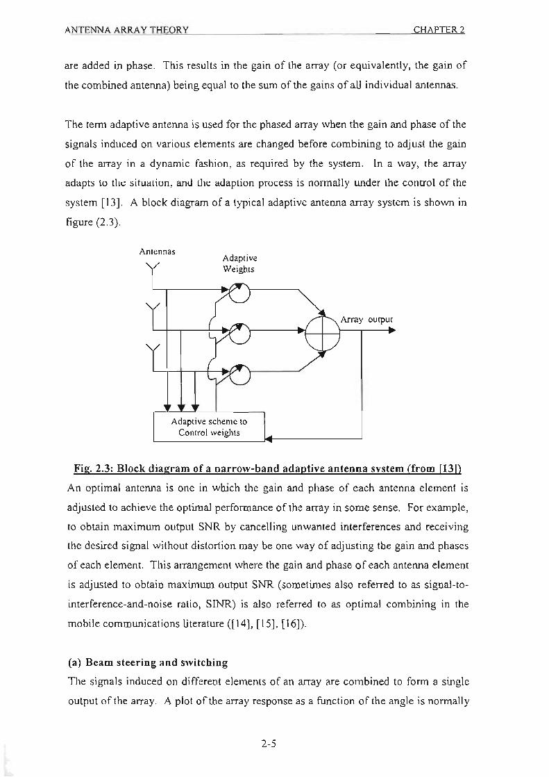
The tenn adaptive antenna is used for the phased array when the gain and phase of the
signals induced on various elements are changed before combining to adjust the gain
of the array in a dynamic fashion, as required by the system. In a way. the array
adapts to the situation. iillU Lh~ adapliun process is normally under the control of the
system [13]. A block diagram of a typical adaptive antenna array system is shown in
figure (2.3).
Antennas Adaptive Weights
Adaptive scheme to Control weights
Array output
Fig. 2.3: Block diagnlm of a narrow-band adaptive antenna system (from (131)
An optimal antenna is one in which the gain and phase of each antenna element is
adjusted to achieve the optimal performance of the array in some sense. For example,
to obtain maximum output SNR by cancelling unwanted interferences and receiving
the desired signal without distortion may be one way of adjusting the gain and phases
of each element. This arrangement where the gain and phase of each antenna element
is adjusted to obtain maximum output SNR (sometimes also referred to as signal-to
interference-and-noise ratio, SlNR) is also referred to as optimal combining in the
mobile communications literature ([14], [15] , [16]).
(a) Beam steering a nd switcbing
The signals induced on different elements of an array are combined to fo rm a single
output of the array. A plot of the array response as a function of the angle is normally
2-5

ANTENNA ARRA Y THEORY CHAPTER 2
referred to as the array pattern or the beam pattern. It is also called a power pattern
when the power response is plotted. It shows the power received by the array at its
output from a particular direction due to a unit power source in that direction. This
process of combining the signals from different elements is known as beamforming.
The direction in which the array has maximum response is said to be the beam
pointing direction. Thus, this is the direction where the array has the ma.ximum gain.
For a linear array, when signals are combined without any gain and phase change, this
is broadside to the array, that is, perpendicular to the line joining all elements of the
array.
The array pattern drops to a low value on either side of the beam pointing direction.
The place of the low value is normally referred to as a null. Strictly speaking, a null is
a position where the array response is zero. However, the term is generally misused
to indicate the low value of a pattern. The pattern between the two nulls on either side
of the beam pointing direct ion is known as the main lobe. The width of the beam
(main lobe) between the two half-power points as called the half-power beamwidth.
These concepts are illustrated in figure (2.4).
Or-~--~------~~--~------~-.
·5 Half-power (3dB
- beam width
'" ~ ~
·10 0
• ~ " It ·15 8.
Sidelobes
~ 0 N .. ·20 E NuBs " 0 z
·25
·~0~-4~-L--~~----~L---~~~-J 20 40 60 80 100 120 140 160
Degrees
Fig. 2.4: A tvrical arrav pattern illustrating some array concepts
A smaller beam width results from an array with a larger extent. The extent of the
array is known as the aperture of the array. Thus, the aperture of the array is the
2-6
ANTENNA ARRAY THEORY CHAPTER 2
distance between the two farthest elements in the array. For a linear array, it is equal
to the distance between the elements on either side of the array.
(b) Conventional beam forming
Adjusting only the phase of signals from different elements to point a beam in a
desired direction is the conventional method of beam pointing or beam forming.
When the main beam is pointed in different directions by adjusting various phases, the
relative positions of the sidelohes with respect to the main lobe change. By adjusting
both the gain and phase of each signal , the pattern can be shaped as required. The
amount of change depends upon the number of elements in the array. When only the
gain of each of the elements are changed, the shape of the array pattern is fixed, that
is, the positions of the sidelobes with respect to the main beam and their levels are
unchanged.
The gain and phase applied to the signals derived from each element may he thought
of as a single complex quantity referred to as the weighting applied to the signals. If
there is only one element, no amount of weighting can change the pattern of that
antenna. With two elements, however, changing the weighting of one element
relative to the other may adjust the pattern to the desired value at one place, that is,
one is able to place one minima or maxima anywhere in the pattern. Similarly with
three elements, two positions may be specified, and so on. Thus, with an N-element
array, one is able to specify N-l positions. These may be one maxima in the direction
of the desired signal and N-2 minimas (nulls) in the directions of unwanted
interferences. This flexibility of an N-element array to be able to fix the pattern at
N-I places is known as the degree of freedom of the array.
(c) Null beam forming
The flexibility of array weighting to being adjusted to specify the array pattern is an
important property. This may be exploited to cancel directional sources operating at
the same frequency as that of the desired source, provided these are not in the
direction of the desired source. In situations where the directions of these
interferences are known, cancellation is possible by placing the nulls in the pattern
corresponding to these directions and simultaneously steering the main beam in the
direction of the desired signal. Beam forming in this way. where nulls are placed in
2-7

ANTENNA ARRAY THEORY CHAPTER 2
the directions of interferences, is nonnally known as null beam fonning or null
steering. The cancellation of one interference by placing a null in the pattern uses one
degree of the freedom of the array.
Null beam fonning uses the direction of sources towards which nulls are placed for
estimating the required weighting on each element. There are other schemes that do
not require directions of all the sources.
2.3 Application of arrays in mobile communication systems [12)
Arrays may be used in various mobile communication systems, for example, base
mobile, indoor-mobile, satellite-mobile, and satellite-to-satellite communication
systems. Only the base-mobile system will be considered here. The use of arrays in
the remaining systems are discussed in [12].
The base-mobile system consists of a base station situated in a cell and serves a set of
mobiles within the celL It transmits signals to each mobile and receives signals from
them. It monitors their signal strength and organizes the handoff when the mobiles
cross the cell boundary. It provides the link between the mobiles within the cell and
the rest of the network.
In this section various scenarios are presented to show how an array could be used in
such a system. The discussion will concentrate on the use of an array at the base
station. A base station having multiple antennas is sometimes referred to as having
antenna diversity or space diversity.
2.3.1 Use of an an-ay at a base station
(a) Formation of multiple beams: Multiple antennas at the base station may be used
to foml mUltiple beams to cover the whole cell site. For example, three beams
with a beamwidth of 12()O each or six beams with a beam width of 600 each may be
fonned for the purpose. Each beam may then be treated as a separate cell, and the
frequency assignment may be perfonned in the usual manner. Mobiles are handed
to the next beam as they leave the area covered by the current beam, as is done in
a nonnal handoffprocess when the mobiles cross the cell boundary.
2-8
ANTENNA ARRAY THEORY CHAPTER 2
(b) Formation of adaptive beams: An array of antennas with the capability to fonn
independent beams may be used at the base station. The array is used to find the
location of each mobile, and then beams are fonned to cover different mobiles or
groups of mobi les. Each beam may he considered as a cochannel cell . and may be
able to use the same frequency or code. as the case may be. Figure (2.5) shows a
typical setup involving different beams covering various mobiles along with the
directions of moving mobiles. It illustrates the situation at two time instants.
~Ii • ¥
• •
Fig. 2.5: A typical setup showing different beams covering various mobiles
This setup is different from the one discussed previously where a number of
beams of fixed shape cover the whole cell . Here, the beams are shaped to cover
traffic. As the mobiles move, the different beams cover different clusters of
mobiles, offering the benefit of transmitting the energy toward the mobiles. The
arrangement is particularly useful in situations where the mobi les move in clusters
or along confined paths, such as highways. Each mobile can also be covered by a
separate beam. Each beam would then follow the mobile, reducing the handoff
problem to the bare minimum.
(c) Null formation: In contrast with steering beams toward mobiles, one may adjust
the antenna pattern such that it has nulls towards other mobiles. Formation of
nulls in the antenna pattern toward cochannel mobiles helps to reduce the
cochannel interference in two ways. In the transmit mode, less energy is
transmitted from the base towards these mobiles, reducing the interference from
2-9

ANTENNA ARRAY THEORY CHAPTER 2
the base to them. In the receiving mode, this helps to reduce the contribution from
these mobiles at the base.
(d) Optimal combining: Canceling unwanted cochannel interferences while an array
is operating in receiving mode is a very effective use of an antenna array. The
process combines signals received on various antennas in such a way that the
contribution due to unwanted interferences is reduced while that due to a desired
signal is enhanced. Knowledge of the directions of the interferences is not
essential to the process's functioning, while some characteristic of the desired
signal are required to protect it from being cancelled.
By using constrained beamfonning techniques, one may he able 10 combine the
formation of nulls in the directions of unwanted mobiles while keeping the
specified response in the direction of a desired mobile. For proper operation, the
direction of the desired signal is required. It is used for maintaining a specified
response in that direction. Though constrained beam-fonning is very effective
when the desired signal is a point source, its use in mobile communications is
limited, particularly in situations of multipaths. Optimal combining using a
reference signal is more appropriate for this case. It requires a signal that is
correlated with the desired signal. The scheme that protects all signals that are
correlated with this reference signal and adds them in phase to maximize their
combined effect. It simultaneously cancels all wavefonns that are not correlated
with this signal, resulting in a removal of cochannel interferences. Thus, optimal
combining using a reference signal is able to make use of mUltipath arrivals of the
desired signal, whereas constrained beamfonning treats them as interferences and
cancels them. Further discussion on these techniques are provided in [13] and
[ 17].
(e) Dynamic cell formation: The concept of adaptive beam-fonning may be
extended to dynamically changing cell shapes [12]. Instead of having cells of
fixed size, the use of array antennas allows the fonnation of a cell based upon
traffic needs, as shown in figure (2.6). An architecture to realize such a base
station requires the capability of locating and tracking the mobiles to adapt the
system parameters to meet the traffic requirements.
2-10

ANTENNA ARRAY THEORY CHAPTER 2
(a) (b)
Fig. 2.6: Cell shape based upon traffic needs. (a) Cells of fixed shape. (b) Cells
of dynamic shape
(I) Blind estimation of cochannel signals: A base station employing arrays may be
able to exploit the fact that signals arriving from different mobiles follow different
paths and arrive at various elements at different times. This allows independent
measurements of signals superimposed from different mobiles. This, along with
the properties of the modulation techniques used, allows separation of signals
arriving from different mobiles. Thus, by using the measured signals at various
elements of the array at the base, one is able simultaneously to separate all signals.
The process is referred to as the blind estimation of cochannel signals ([12], [13],
[1 7]). It does not require knowledge of the directions or other parameters
associated with mobiles, such as a reference signal, but exploits the temporal
structure that might exist in signals inherited from the source of their generation,
for example, the modulation techniques used.
2.3.2 Performance improvement usine: an array
An antenna array is able to improve the performance of a mobile communication
system in a number of ways. It provides the capabi lity to reduce cochannel
interferences and multipath fading, resulting in better quality of services, such as
reduced bit error rate (BER) and outage probability. Its capability to form multiple
beams could be exploited to serve many users in parallel resulting in an increased
2-11
ANTENNA ARRAY THEORY CHAPTER 2
spectral effic iency. Its ability to adapt beam shapes to suit traffic conditions is useful
in reducing the handoffrate.
This section discusses the advantages of an array of antennas in a mobile
communications system and improvements that are possible by using multiple
antennas in a system rather than a single one.
(a) Reduction in delay spread and multipath fading 112): Delay spread is caused
by multipath propagation where a desired signal arriving from different directions
gets delayed due to the different travel distances involved. An aITay with the
capability to form beams in certain directions and nulls in the others is able to
cancel some of these delayed arrivals in two ways. In the transmit mode, it
focuses energy in the required direction, which helps to reduce multipath
reflections causing a reduction in the delay spread. In the receive mode, an
antenna array provides compensation in multi path fading by diversity combining,
by adding the signals belonging to different clusters after compensating for delays,
and by canceling delayed signals arriving from directions other than that of the
main signal.
(i) Use of diversity combining: Diversity combining achieves a reduction in
fading by increasing the signal level based upon the level of signal strength
at different antennas, whereas in multi path cancellation methods, it is
achieved by adjusting the beam pattern to accommodate nulls in the
direction of late arrivals, assuming them to be interferences. For the latter
case, a beam is pointed in the direction of the direct path or a path along
which a major component of the signal arrive, causing a reduction in the
energy received from other directions and thus reducing the components of
multipath signal contributing to the receiver.
(ii) Combining delayed arrivals: A radiowave originating from a source
arrives at a distant point in clusters after getting scattered and reflected
along the way. This is particularly true in scenarios with large buildings
and hills were delayed arrivals are well separated. These clustered signals
could be used constructively by grouping them as per their delays
compared to a signal available from the shortest path. Individual paths of
2-12

ANTENNA ARMY THEORY CHAPTER 2
these delayed signals may be resolved by exploiting their temporal or
spatial structure.
The resolution of paths usmg temporal structures depends upon the
bandwidth of the signal compared to the coherence bandwidth of the
channel and increases as this bandwidth increases. When the paths are
well separated spatially. an antenna array may be used. This could be
done, for example, by detennining their directions. In some situations, it is
possible to separate the signals from each cluster by formi ng multiple
beams in the directions of each component of these clusters, with nulls
pointing toward the other ones. Combining signals belonging to different
users after compensating for delays leads to a reduction in delay spread
and cochannel interference.
(iii) NlIlling delayed arrivals: An antenna array can reduce delay spread by
nulling the delayed signals arriving from different directions.
(b) Reduction in cocbannel interference: An antenna array has the property of
spatial filtering, which may be exploited in transmitting and receiving modes to
reduce cochannel interferences. In the transmitting mode, it can be used to focus
radiated energy by forming a directive beam in a small area where a receiver is
likely to be. This in turn means that there is less interference in other directions
where the beam is not pointing. Cochannel interference in transmit mode could be
further reduced by forming specialized beams with nulls in the direction of other
receivers. This scheme deliberately reduces transmitted energy in the direction of
cochannel receivers and requires knowledge of their positions.
The reduction of cochannel interference in the receive mode is a major strength of
antenna arrays. It does not require knowledge of the cochannel interferences. If
these were available, however, an array pattern might be synthesized with nulls in
these directions. In general, an adaptive array requires some information about
the desired signal, such as the direction of its source, a reference signal, or a signal
that is correlated with the desired signal.
2- 13
ANTENNA ARRAY THEORY CHAPTER 2
(c) Spectral efficiency and capacity improvement: Spectrum efficiency refers to
the amount of traffic a given system with certain spectrum allocation could
handle. An increase in the number of users of the mobile communications system
without a loss of perfonnance causes the spectrum efficiency to increase. Channel
capacity refers to the maximum data rate a channel of given bandwidth could
sustain. An improved channel capacity leads to more users of a specified data
rate, implying a better spectral efficiency.
TDMA and CDMA result in an increase in channel capacity over the standard
FDMA, allowing different time slots and different codes to be assigned to
different users [18]. This may be further improved by using multiple antennas and
combining the signals received from them. Firstly, the increased quality of
service resulting from the reduced cochannel interferences and reduced multipath
fading, as discussed, may be traded to increase the number of users. Thus, the use
of an array results in an increase in channel capacity while the quality of service
provided by the system remains the same, that is, it is as good as that provided by
a system using a single antenna. Secondly, an array may be used to create
additional channels by fonning multiple beams without any extra spectrum
allocation, which results in potentially extra users and thus increases the spectrum
efficiency.
(i) Mllltiple-beam alltelllla array at the base stal;oll: By first using a base
station array in receive mode to locate the positions of mobiles in a cell
and then transmitting in a multiplexed manner toward different clusters of
mobiles one at a time, using the same channel, the spectral efficiency
increases many times over and depends upon the number of elements in
the array and the amount of scattering in the vicinity of the array. By
pointing beams with directed nulls towards other mobiles in a cell, the
array is used more efficiently than by reducing the cell size and the reuse
distance. The use of a multiple-beam antenna array at the base-station to
Improve spectral efficiency by resolving the angular distribution of
mobiles is discussed in [3], where it is shown that spectral efficiency
increases as the number of beams increases. Fonnulas, which are helpful
in predicting interference reduction and capacity increase provided by a
switched-beam antenna system employed by a base station, also predict
2-14

ANTENNA ARRAY THEORY CHAPTER 2
that the number of subscribers in a cell increases as the number of beam
increases [19].
(ii) Alltelllla array at a CDMA base statio,,: By using an array of antennas for
a CDMA system, the number of mobiles a cell may be able to sustain
increases many fold (on the order of the number of elements) for a given
outage probability and bit error rate (BERl ([15], [20], [21]). For example,
at an outage probability 0[0.01, the system capacity increases from 31 for
a single antenna system to 115 for a five-element array_ Using an array of
seven elements increases the capacity to 155 [21 ]. The study reported in
[15] is for both mobile-to-base and base-to-mobi le links and derives
expressions for the outage probability considering the effects of cochannel
interferences
(d) BER improvement: A consequence of a reduction in cochannel interference and
multipath fading by using an array in a mobile communications system to improve
the communications quality is a reduction in BER and symbol error rate (SER) for
a given signal-to-noise ratio (SNR), or a reduction in required SNR for a given
BER.
(el Reduction in outage probability: Outage probability is the probability of a
channel being inoperative due to increased error rate in the received data. It may
be caused by cochannel interference in a mobile communications system. Using
an array helps to reduce outage probability by decreasing cochannel interference.
It decreases as the number of beams used by a base station increases.
(0 Increase in transmission efficiency: Electronically steerable antennas are
directive compared to fixed omnidirectional antennas, that is, they have high gains
in the directions where the beam is pointing. This fact may be useful in extending
the range of a base station resulting in a bigger cell size, or it may be used to
reduce the transmitted power of the mobiles. By using a highly directive antenna,
the base station may be able to pick a weaker signal within the cell than by using
an omnidirectional antenna. This in turn means that the mobile has to transmit
less power and its battery will last longer, or it would use a smaller battery,
resulting in a smaller size and weight. This is important for hand-held mobiles.
2-15
ANTENNA ARRAY THEORY CHAPTER 2
It is also advantageous to use an antenna array at the base station iO transmit
mode. In a single antenna system, all the power of the base station is transmitted
by one antenna. However, when the base station uses an array of antennas and
transmits the same amount of power as that of the single antenna system, the
power transmitted by each antenna of the array is much lower compared to the
case where the total power is transmitted by one antenna. Furthennore, for a
given SNR at the mobile site, the base station using an array has to transmit less
power compared to the single omnidirectional antenna due to the directive nature
of the array. This further reduces the power transmitted by each antenna. These
reductions in transmitted power level using an array allow the use of electronic
components of lower power rating in the transmitting circuitry. This results in
lower system cost, leading to a more efficient transmission system.
(g) Dynamic channel assignment: Ln mobile communications, channels are
generally assigned in a fixed manner depending upon the position of a mobile and
the available channels in the cell where the mobi le is positioned. As the mobile
crosses the cell boundary, a new channel is assigned. In this arrangement, the
number of channels in a cell are nonnally fixed. The use of an array provides an
opportunity to change the cell boundary and thus to allocate the number of
channels in each cell as the demand changes due to changed traffic situations.
This provides the means whereby a mobile or group of mobiles may be tracked as
it moves and the cell boundary may be adjusted to suit this group.
Dynamic channel assigrunent is also possible in a fixed cell boundary system and
may be able to reduce the frequency reuse factor up to a point where frequency
reuse in each cell might be possible. There may be situations when it is not
possible to reduce cochannel interferences in certain channels, and the call may be
dropped due to high BER caused by strong interferences. Such a situation may
arise when a desired mobile is close to the cell boundary and the cochannel
mobiles are near the desi red mobile's base-station. This could be avoided by
dynamic channel assignment, where the channel of a user is changed when the
interference is above a certain level.
2-16

ANTENNA ARRAY THEORY CHAPTER 2
(h) Reduction in handoff rate: When the number of mobiles in a cell exceeds its
capacity. cell capacity is used to create new cells, each with its own base-station
and new frequency assignment. A consequence of this is an increased handoIT
due to reduced cell size. This may be reduced using an array of antennas. Instead
of cell splitting, the capacity is increased by creating independent beams using
more antennas. Each beam is adapted or adjusted as the mobile locations change.
The beam follows a cluster of mobi les or a single mobile. as the case may be. and
no handoffis necessary as long as the mobiles served by different beams using the
same frequency do not cross each other.
(i) Reduction in cross talk: Cross talk may be caused by unknown propagation
conditions when an array is transmitting multiple cochannel signals to various
receivers. Adaptive transmitters based upon the feedback obtained from probing
the mobiles could help eliminate this problem. The mechanism works by
transmitting a probing signal periodically. The received feedback from mobiles is
used to identify the propagation conditions, and this infonnation is then
incorporated into the beamfonning mechanism.
2.4 Demonstration of beamscanning using linear arrays
2.4.1 The linear array
Appendix A. I shows and describes the three dimensional coordinate system used in
this section to analyze the array response as a result of beamscanning. The
mathematical models developed here may be found in one fonn or another in many
texts on array theory, see for example (12], (13] and [54].
Consider a N element linear array of isotropic point sources placed along the z-axis as
shown in figure (2.7). The elements are spaced a distance d apart from one another.
Assume that all elements have identical amplitudes hut each succeeding element has a
p progressive phase lead current excitation relative to the preceding one (p represents
the phase by which the current in each element leads the current of the preceding
element). An array of identical elements all of identical magnitude and each with a
progressive phase is referred to as a unifonn array. Although isotropic elements are
not realizable in practice, they are a useful concept in array theory, especially for the
2·17

ANTENNA ARRAY THEORY CHAPTER 2
computation of radiation patterns. The effect of practical elements with nonisotropic
elements will be considered in section (2.4. 1.1).
N
r,
r,
r,
r,
y
dcos9
Fig. 2.7: Far-field 2.eometrv of N element array of isotropic point sources
positioned along the z-axis
The time delay of a signal between two successive elements is given by:
dcosB T = =""'-
c where c is the free-space signal propagation velocity.
This time delay corresponds to a phase shift of
/If = lVT + fJ
= 27rf d cosB + fJ c
27r =-dcosB+fJ
A. = kdcosB+ fJ
where f is the frequency and k = 21r is the wave number. A.
(2.1 )
(2.2)
The array factor (AF) is now introduced. It is basically a mathematical concept that is
a function of the time delay (or phase shift) between the array elements. For a
uniform array. the array factor is given by
2-18

ANTENNA ARRAY THEORY
AF = I + e +}(kdC058+P) + e+ j2 (kdcosO+/J) + .... + e + ,(N-1Xkdo;os8+/J)
N = L e+)(II-1X-Wo;osO+P)
.,' which can be written as
.,' where If = kd cosB + fJ
CHAPTER 2
(2.3)
(2.4)
Since the total array factor for the uniform array is a summation of exponentials, it
can be represented by the vector sum of N phasors each of unit amplitude and
progressive phase 't' relative to the previous one. Graphically this is illustrated by the
phasor diagram in figure (2.8). _._---IL(N - I) 'V
#N #4
I L341 3'4'
#2
Fig. 2.8: Phasor diagram of N element linear array It is apparent from the phasor diagram that the amplitude and phase of the AF can be
controlled in uniform arrays by properly select ing the relative phase 't' between the
elements.
The array factor of equation (2.4) can also be expressed in an alternate, compact and
closed form whose functions and their distribution are more recognizable. This is
accomplished as follows:
Multiplying both sides of equation (2.4) by ei'l' it can be wrinen as
(AF)e i ll' = e ifll + e l 2!" + e j3\1' + .... + e J(N- I)1I' + e jN'(I (2.5)
Subtracting equation (2.4) from equation (2.5) reduces to
(2.6)
which can also be written as
2-19

ANTENNA ARRAY THEORY CHAPTER 2
AF = e - = e il(N-I)12],- e - e = eil(N-I)12]'- 2 (2.7) [ jN. I] [ j(Na). -j(NI». ] [Sin( N VI)] j" - 1 ej (l / 2)1'" _ e-J( 1/ 2)\I" • 1
e sm(- Vl) 2
If the reference point is the physical centre of the aTTay, the aTTay factor of equation
(2.7) reduces to
AF= 2 [
Sin( N VI)]
sin(~VI) 2
(2.8)
The maximum of equation (2.8) occurs when "{l=O but the aTTay factor (AF) is
indeterminate since both the numerator and denominator are zero. However, by
applying L'Hopital 's rule (differentiating numerator and denominator separately) and
setting "{l=O results in equation (2.8) having a maximum value ofN. To normalize the
array factors so that the maximum value of each is unity, equation (2.8) is written in
the normalized form as
(AF). = ~[Sin(tVl)] sin(- Vl)
2
where 'I' = kd cos B + P
2.4.1.1 Principle of pattern multiplication
(2.9)
The reasons for using isotropic elements for computation of the array factor becomes
apparent in the ensuing discussion. The array factor is a function of the geometry of
the array and the excitation phase. By varying the separation d and andlor the phase p
between the elements, the characteristics of the array factor and of the total field of
the array can be controlled. The far~zone field of a uniform array of identical
elements is equal to the product of the field of a single element, at a selected reference
pOi"t (usually the origin), and the array faclOr of that array [11]. That is
E(total) = [£(singleelemellt at reference point)] x [array faclor
ET = EeE(J (2.10)
This is referred to as pattern multiplication for arrays of identical elements. Each
array has its own array factor. The array factor, in general, is a function of the number
2-20

ANTENNA ARRAY THEORY CHAPTER 2
of elements, their geometrical arrangement, their relative magnitudes, their relative
phases, and their spacing. Since the array factor does not depend on the directional
characteristics of the radiating elements themselves, it can be fonnulated by replacing
the actual elements with isotropic (point sources). Once the array factor has been
derived using the point source array, the total field of the actual array is obtained by
use of equation (2.10). Each point source is assumed to have the ampli tude, phase
and location of the corresponding element it is replacing. Squaring both sides of
equation (2.10) converts it into a relationship of power density-patterns (radiation
patterns) in which the squares of the electric-intensity factors may be replaced by
corresponding power-density pattern factors i.e. p. = pp. r ' "
in using the principle of pattern multiplication, certain rules must be observed [25]:
(a) The pattern to be used for the array elements is the pattern that a single element
would have ifit were isolated, that is, not in the "array envi.ronment".
(b) The array pattern to be used is the one calculated fOT isotropic point-source
elements spaced and phased the same as the actual elements. The phasing cannot
be calculated on the basis of a transmission-line feed system designed for the
input impedances of the elements operating as isolated elements. Their actual
input impedances will be affected by mutual coupling with other elements.
(c) All the array elements must be alike; they must have similar patterns, similarly
orientated. For example, if the elements are dipoles, they must have their axes
parallel to one another. If the elements are horns, they must be of the same fonn
and size, and all "aimed" in the same direction.
Equation (2.10) is only an approximation for many problems of array design. It
ignores mutual coupling (section (2.5)) and it does not take account of the scattering
or diffraction of radiation by the adjacent array elements. These effects cause the
element pattern to be different when located within the array in the presence of the
other elements than when isolated in free space. In order to obtain an exact
computation of the array radiation pattern, the presence of each element must be
measured in the presence of all the others. The array pattern may be found by
summing the contributions of each element, taking into account the proper amplitude
and phase.
2-21

ANTENNA ARRAY THEORY CHAPTER 2
2.4.1.2 Phased (scanning) array
In many applications it is desired to orientate/steer the maximum radiation in a
particular direction to ronn a scanning array. Assume that the maximum radiation of
the array is required to be oriented at an angle So (00 ~ So ~ 18(0). Referring to
equation (2.9), the maximum of the array factor occurs when 'f'=0,
\If = kd cosB + Ill .... = 0
=> 11 = -kd cosB,
The array factor of equation (2.9) now becomes
(2.11 )
sin[Nm:1 (COSB-cosBJ]
(AF) . = ~ (2.12)
NSin[ T (COSB-coSBJ]
Two arrays that are of interest are the broadside and the end fire arrays. In the
broadside array, the maximum radiation is directed nonna! to the axis of the array
(e = 90<> in figure (2.7». Substituting 9, = 90<> into equation (2.11) yields p = O. Thus
for a broadside array, the elements have zero progressive phase lead current
excitation. However, it is necessary that all the elements have the same phase
excitation (in addition to the same amplitude excitation). For an endfire array, the
maximum radiation can be directed at either 90
= 00 or 1800 i.e. along the axis of the
array. To direct the maximum toward 90
= 00, the progressive lead current excitation
(p) should be - kd while if the maximum is desired towards e, = ISO<>, then p = kd.
2.4.1.3 Antenna element spacing to avoid grating lobes
One of the objectives in many designs is to avoid multiple maxima, in addition to the
main maximum, which are referred to as grating lobes. A grating lobe is defined as a
lobe, other than the main lobe, produced by an array antenna when the interelement
spacing is sufficiently large to pennit the in-phase addition of radiated fields in more
than one di rection. They are undesirable since, in addition to directing the main lobe
in the desired direction, the array also directs grating lobes to undesired directions.
Thus there is no maximization of power in the desired direction. Often it may be
required 10 select the largest spacing between the elements but with no grating lobes.
2-22

ANTENNA ARRAY THEORY CHAPTER 2
Consider a broadside array (fJ = 0 and 'I' = kd cosO = 27r d cosO). This value of \jI A
when substituted in equation (2.9) makes the array factor attain its maximum value
when casO = IIA for n = 1,2,3, ... The maximum at cosO = 0 defines the main beam. d
If the spacing between elements is a half-wavelength (d = 0.5),), the first grating lobe
(n = ± l ) does not appear in real space since cosO = 2 which is undefined. Grating
lobes appear at ()o and 18()O when d = A' For a nonscanning array this condition
(d = ,..) is usually satisfactory for the prevention of grating lobes. Practical antenna
elements that are designed to maximize the radiation at e = 900, generally have
negligible radiation in the directions e = ()o and e = 18()O directions. To avoid any
grating lobe in a nonscanning array, the largest spacing between the elements should
be less than one wavelength (dmax
< ),J.
Using an argument similar to the nonscanning array described above, for a scanning
array, grating lobes appear at an angle 8g
when the array factor of equation (2.12)
attains its maximum value, or
: (cosO. -cOSOJ=±II7r
d ± 11 or - = ;---:-='-----,--;
A IcosB, -cosB,,1
(2.13)
If a grat ing lobe is pennitted to appear at 8g
= ()o when the main beam is steered to
80
= 18()O, it is found from equation (2.13) that d = '),/2. Thus the element spacing
must not be larger than a half-wavelength if the beam is to be steered over a wide
angle without having undesirable grating lobes. Therefore a criterion for determining
the maximum element spacing for an array scanned to a given angle 80
is to set the
spacing so that the nearest greatest lobe is at the boundary of the visible region.
Using equation (2.13) this leads to the condition
d I A ,;; "11---'co'-s-=o.' 1
(2.14)
Therefore the common rule that half-wave spacing precludes grating lobes is not quite
accurate, as part of the grating lobe may be visible for extreme scan angles.
2-23

ANTENNA ARRAY THEORY CHAPTER 2
Grating lobes can also be avoided by unequal spacing of the elements i.e. by making
the array aperiodic [8]. In an aperiodic array, the element weights are made equal but
all the design freedom is employed in the element locations. There is no restriction
imposed on the element spacing. However, the elements are usually overspaced to
avoid the effect of mutual coupling. This process of overspacing the array is known
as thinning [8]. In addition to the hazard of grating lobes, which is avoided by
unequal spacing of the elements, a thinned alTay introduces another problem. For an
array of fixed length, the number of elements is reduced. While this lowers cost and
mutual coupling, both highly desirable changes, the reduction in element numbers
reduces the designer's control of the radiation pattern in the sidelobe region. This
reduction in design control influences the level of the peak sidelobe, which is of major
concern to the alTay designer. Since the number of degrees of freedom is reduced in
direct proportion to the number of elements, deviations from the desired radiation
pattern must be anticipated. The beam width and approximate shape of the main lobe
are not severely altered by thinning (beam width is not affected since the length of the
array is fixed). The dominant effect of thinning is observed in the sidelobes. [8]
provides a detailed discussion on aperiodic arrays and thinning.
2.4. t.4 Simulation work
Appendix A.2 contains a MA TLAB program for the analysis of linear arrays using the
theory developed thus far. The program plots the array factor pattern (for elements
placed along the z-axis) as a function of the number of elements, element spacing and
scan angle. An extension is also made to illustrate the pattern multiplication rule
(section 2.4.1.1) using the half-wavelength dipole antenna as the element. The
concept of grating lobes is also illustrated.
2-24

ANTENNA ARRAY THEORY CHAPTER 2
2.5 Mutual coupling
Up until now, no discussion or definition of mutual coupling was given. The
principal effects of mutual coupling are changing the effective/predicted element
pattern and producing gain variations in scanning. Due to this detrimental effect on
array perfonnance, it needs to be considered during array design. A brief description
of this phenomenon is thus warranted.
When two antennas are near each other, whether one and/or both are transmitting or
receiv ing, some of the energy that is primarily intended for one ends up at the other.
The amount depends primari ly on the
(a) radiation characteristic of each element
(b) relative separation between them
(c) relative position/orientation of each element in the array
Cd) feed of the array elements
(e) scan volume of the array
There are many di fferent mechanisms that cause this interchange of energy. For
example, even if both antennas are transmitting, some of the energy radiated from
each will be received by the other because of the nonideal directional characteristics
of practical antennas. Part of the incident energy on one or both antennas may be
rescattered in different directions allowing them to behave as secondary transmitters.
This interchange of energy is known as mutual coupling, and in many cases it
complicates the analysis and design of an antenna.
In the theory developed thus far, it was implicitly assumed that each element in the
array acts independently of all the others. This assumption is invalid in practice.
Currents couple from one element to another by the parts illustrated in figure (2.9).
2-25
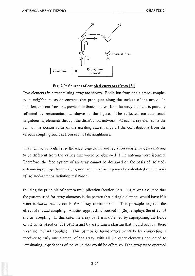
ANTENNA ARRAY THEORY
Generalor
~/ r r
Distribution network
Phase shifters
Fig. 2.9: Sources of coupled currents (from 18])
CHAPTER 2
Two elements in a transmitting array are shown. Radiation from one element couples
to its neighbours, as do currents that propagate along the surface of the array. In
addition, current from the power-distribution network to the array element is partially
reflected by mismatches, as shown in the figure. The reflected currents reach
neighbouring elements through the distribution network. At each array element is the
sum of the design value of the exciting current plus all the contributions from the
various coupling sources from each of its neighbours.
The induced currents cause the input impedance and radiation resistance of an antenna
to be different from the values that would be observed if the antenna were isolated.
Therefore, the feed system of an array cannot be designed on the basis of isolated
antenna input impedance values, nor can the radiated power be calculated on the basis
of isolated-antenna radiation resistance.
In using the principle of pattern multiplication (section (2.4.1.1 », it was assumed that
the pattern used for array elements is the pattern that a single element would have if it
were isolated, that is, not in the "array environment" . This principle neglects the
effect of mutual coupling. Another approach, discussed in [26], employs the effect of
mutual coupling. In this case, the array pattern is obtained by superposing the fields
of elements based on this pattern and by assuming a phasing that would occur if there
were no mutual coupling. This pattern is found experimentally by connecting a
receiver to only one element of the array, with all the other elements connected to
tenninating impedances of the value that would be effective if the array were operated
2-26

ANTENNA ARRA Y THEORY CHAPTER 2
nonnally. This element pattern is measured physically. The currents induced in the
single receiving element (as well as in the terminating elements) will be the same as
in actual array operation, including mutual coupling effects. The pattern measured
under these conditions is called "the element pattern in the array environment," and it
is in general different from the pattern of an isolated element. In the practical design
of arrays, the effects of mutual coupling are often evaluated experimentaJly, since
theoretical calculation is quite difficult, although the theory is helpful in
understanding the general nature of the effect.
Mutual coupling effects are greatest for closely spaced elements. It is also greater in
an endfire array than in a broadside array. It can be reduced by overspacing the
elements in the array (thinning). For an array of fixed length, thinning results in
fewer elements, and hence, lower costs. These salutary effects, however are
accompanied by grating lobes unless the array is made aperiodic (as discussed in
section (2.4.1.3)) [8]. Thinning also reduces the designer's control of the radiation
pattern in the sidelobe region.
2-27

ANALOGUE AND DIGiTAL BEAMFORMTNG CHAPTER 3
CHAPTER 3
ANALOGUE AND DIGITAL BEAMFORMING
3.1 Introduction
The tenn beamfonning relates to the function perfom1ed by a device or apparatus in
which energy radiated by an antenna is focused along a specific direction in space.
The objective is to preferentially receive or to transmit a signal from that direction.
Energy from a source, which is assumed to be aligned with the antenna's preferred
direction, arrives at the feed temporary aligned and is thereby summed coherently. In
general, sources in other directions, arrive at the feed unaligned and add incoherently.
For this reason, beamfonning is often referred to as spatial filtering.
When an array is illuminated by a source, samples of the source's wavefront are
recorded at the location of the antenna elements. The outputs from the antenna
elements can be subjected to various forms of signal processing, wherein phase or
amplitude adjustments are made to produce outputs that can provide concurrent
angular infonnation fo r signals arriving in several different directions in space. When
the outputs of the elements are combined via some passive phasing network, the
phasing will usually arrange for the outputs of all the elements to add coherently (in
phase) for a given direction. The network that controls the phases and amplitudes of
the excitation currents is usually called the beamfonning network.
The weight and summing circuits of an adaptive antenna (figure (2.3) chapter 2) can
operate at the antenna RF operating frequency, at a lower (downconverted) IF
fTequency or at baseband. At RF or IF. beam forming may be performed using
analogue phase shifters and attenuators [27]. Altematively, digital teclmology may be
used at baseband. Digital teclmology may also be used at IF depending on the IF
frequency. This chapter explores the implications, with respect to implementation, of
adapting the antenna weights at RF, IF and baseband.
3-1
ANALOGUE AND DIGITAL BEAMFORMING CHAPTER 3
3.2 Analogue or digital beamforming?
Adaptive arrays may have either analogue or digital processing for the determination
of the array element weight matrix. In the analogue case, all the received signals in
the array are analogue, the usual operations performed by the analogue processor
being frequency conversion, multiplication, correlation, integration, filtering, and so
on. In an adaptive array with digital processing, all signals (analogue) received by the
antenna are converted to digital fonn using analogue to digital converters (ADC) with
the signal being processed subsequently only in this form. Sometimes, a digital to
analogue converter (DAC) is used to provide an analogue output signaL It may be
noted that chronologically, the first built were analogue systems [28], [29]. However,
taking account of the impact ofVLSI circuit development on this field , the situation is
swiftly changing in favour of digital processors. The interest in digital
implementation is further enhanced by its potential use in satellite communication
systems where size, weight and power consumption become important design factors.
Also technological advances in digital signal processing provide the possibi li ty of
developing a digital receiver. If such a receiver can be achieved, its performance may
be superior in compari son to a conventional analog approach because of three major
differences [30]:
(a) More information is maintained in the digital approach.
(b) The digitized data can be stored for long periods of time.
(c) More flexible signal processing methods are available to obtain the desired
information directly from digitized signals.
3-2

ANALOGUE AND DIGITAL BEAMFORMING CHA PTER 3
3.3 Analogue beamforming
If beamforming is carried out at RF or IF, the analog beamforming network usually
consists of devices that change the phase and power of the signals. Figure (3.1) gives
an example of a RF beamfonner that is designed only to form one beam.
Antenna rlr---I--- -l-----'f--I'lements
I
l~_H'_ .H._H_n .. n_ n_H. __ n __ l ::,::::::~;:~ Beamforming network
Fig. 3.1: An analog beamforming network (from [l 7D
It should be noted that an analog beam forming network consists of devices such as
phase shifters and power dividers which are used to adjust the amplitude and phases
of the antenna signals in such a way as to form a desired beam. It is sometimes
desirable to form multiple beams that are offset by finite angles from each other. The
design of a multiple-beam beam forming network is much more complicated than that
of a single-beam beam forming network. A multiple-beam beamforming network is
known as a beam forming matrix. The best example is given by the Butler matrix
[31]. In a beamforming matrix, an array of hybrid junctions and fixed phase-shifters
are used to achieve multiple beams.
3.3.1 Arrav feeds
If a single transmitter and receiver are utilized in an array, there must be some fonn of
network to connect the single port of the transmitter and/or receiver to each of the
antenna elements. The power divider used to connect the array elements to the single
port is called an array feed. There are at least three basic concepts for feeding an
array: the constrained feed, the optical space feed and the parallel plate feed ([32],
[33] , [34]). The constrained feed utilizes waveguide or other microwave transmission
lines along with couplers, junctions or other power distribution devices. The optical
space feed distributes the energy to a lens array in a manner analogous to a point-feed
illuminating a lens or reflector antenna. The advantage of an optical beam-forming
feed over the constrained feed is simplicity. Disadvantages are a lack of ampl itude
tapering control and the excessive volume of physical space required to accommodate
the feed system. The parallel plate feed uses the principles of microwave structures to
3·3

ANALOGUE AND DIGITAL BEAMFORMING CHAPTER 3
provide efficient power division. It is in some respects. a cross between the
constrained feed and the optical space feed . The constrained feed is the commonest
type of feed system and therefore warrants a further discussion. [33] and [34] provide
a detailed description on the other two feed systems.
3.3.1.1 The constrained feed
The various types of constrained feeds ean bc classified into two groups: the series
feed and the parallel feed. A description of the various types of feeds in each group
fo llows.
Ca) Series reed
In the series-fed arrangement, the energy may be transmitted from one end of the line
(figure 3.2(a)), or it maybe fed from the centre out to each end (figure 3.2(b».
Fig. 3.2(3): End-fed series feed with series phase shifters
•
Fig. 3.2(b): Centre-fed series feed with series phase shifters
The elements are arranged serially along the main line. They consist of a main
transmjssion line from which energy is tapped (in the case of transmission) through
loosely coupled junctions to feed the radiating elements. The path length to each
radiating element must be computed as a function of frequency and taken into account
when setting the phase shi fter. The adjacent elements are connected by a phase
shifter with phase shift cp. All the phase shifters are identical and introduce the same
amount of phase shift, which is less than 2n radians. To steer the beam, phase shifters
3-4
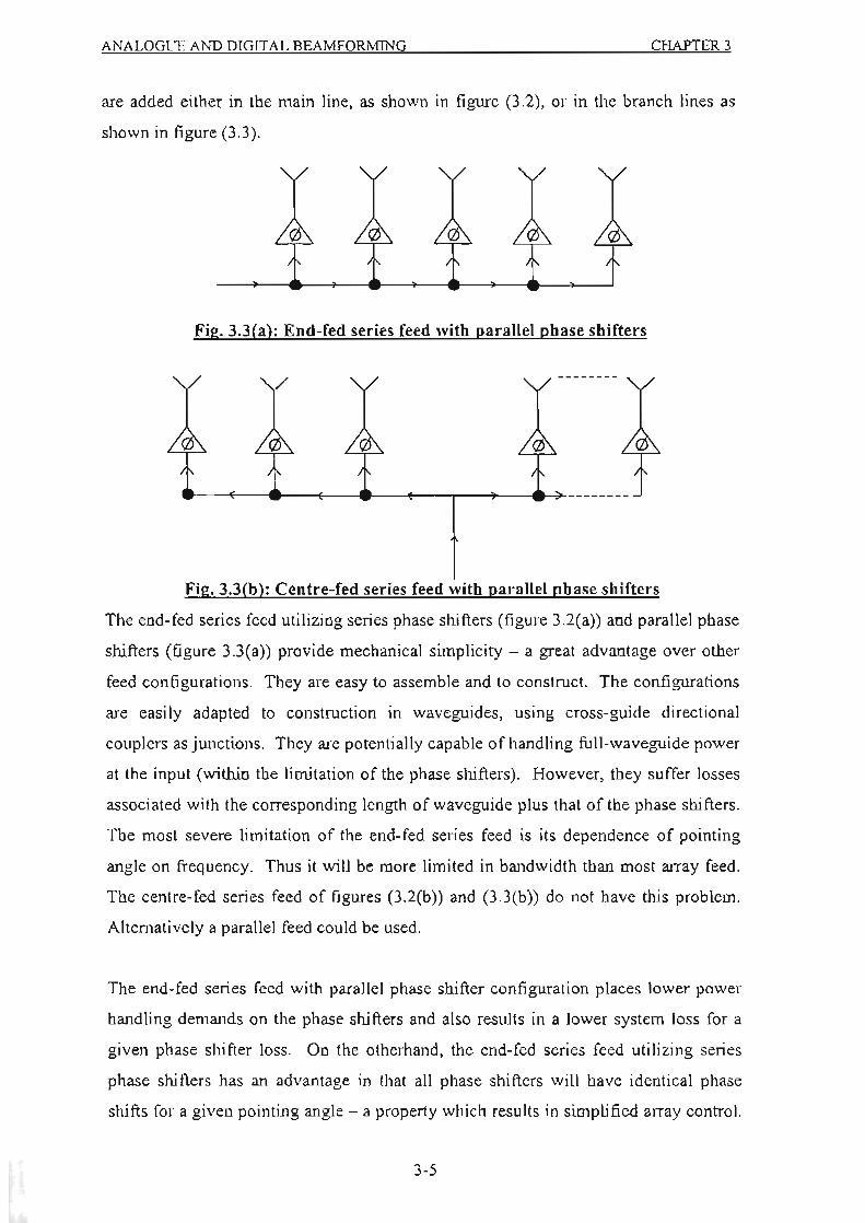
ANALOGUE AND DIGITAL BEAMFORMJNG CHAPTER 3
are added either in the main line, as shown in figure (3.2), or in the branch lines as
shown in figure (3.3).
Fig. 3.3(a): End-fed series feed with parallel phase shifters
_-<-~f-_"""'_-,--_~-+--------
Fig. 3.3(b): Centre-fed series feed with parallel phase shifters
The end-fed series feed utilizing series phase shifters (figure 3.2(a)) and parallel phase
shifters (figure 3.3(a)) provide mechanical simplicity - a great advantage over other
feed configurations. They are easy to assemble and to construct. The configurations
are easi ly adapted to construction in waveguides, using cross-guide direct ional
couplers as junctions. They are potentially capable of handling ful l-waveguide power
at the input (within the limitation of the phase shifters). However, they suffer losses
associated with the corresponding length of waveguide plus that of the phase shifters.
The most severe limitation of the end-fed series feed is its dependence of pointing
angle on frequency. Thus it will be more limited in bandwidth than most array feed.
The centre-fed series feed of figures (3.2(b)) and (3.3(b)) do not have this problem.
Alternatively a parallel feed could be used.
The end-fed series feed with parallel phase shifter configuration places lower power
handling demands on the phase shifters and also results in a lower system loss for a
given phase shifter loss. On the otherhand, the end-fed series feed utilizing series
phase shifters has an advantage in that all phase shifters will have identical phase
shifts for a given pointing angle - a property which results in simplified array control.
3-5

ANALOGUE AND DIGITAL BEAMFORMING CHAPTER]
However, the total system loss of the end-fed series feed with series phase shifters is
higher than that utilizing parallel phase shifters. The bandwidth of a series feed can be
increased by making the path lengths from the input to each output of the branch lines
all equal as shown in figure (3.4).
Fie. 3.4: Equal-path-length series feed
However, if the bandwidth is already limited by the phase shifters and the couplers,
very little benefit can be derived from this approach at the cost of a considerable
increase in size and weight. The network of figure (3.4) simplifies the beam-steering
computation since the correction for path-length differences is no longer necessary.
(a) Parallel feeds
The frequency dependence (change in beam-pointing angle with frequency)
associated with series feeds can be reduced by the use of parallel feeds at a cost of a
slightly more complex mechanical structure. The frequency dependence of the
parallel-feed configuration depends mainly on the frequency characteristics of the
phase shifters and the couplers at the junctions of the feed, if the line lengths from the
transmitter (or receiver) to the radiators are all made equal. Thus, if variable time
delay phase shifters were used in place of the constant-phase type phase shifters at
each radiating element, the beam pointing angle would be essentially independent of
3-6

ANALOGUE AND DIGITAL BEAMFORMING CHAPTER 3
frequency. The frequency dependence of a parallel feed using constant-phase-type
phase shifters is discussed in section (3 .3.3).
The most common technique for realizing parallel feeds is the corporate feed structure
of figure (3 .5).
Fie:. 3.5: Corporate feed
The energy to be radiated is divided between the elements by power spiitters. Equal
lengths of line transmits the energy to each element so that no unwanted phase
differences are introduced by the lines themselves. If the lines are not of equal length.
a compensation in the phase shift must he made. The proper phase change for beam
steering is introduced by the phase sbifters in each of the lines feeding the elements.
When the phase of the first element is taken as the reference, the phase shifts required
in the succeeding elements are $, 2$, 3$, .... , (N- I) $.
The maximum phase change required of each phase shifter in the parallel-fed array is
many times 27t radians. Since phase shift is periodic with period 27t, it is possible in
many applicat ions to use a phase shifter with a maximum of 27t radians. However, if
the pulse width is short compared with the antenna response time (if the signal
bandwidth is large compared with the antenna bandwidth), the system response may
be degraded. For example, if the energy were to arrive in a direction other than
broadside, the entire array would not be excited simultaneously. The combined
outputs from the parallel-fed elements will fail to coincide or overlap, and the
received pulse will be smeared. This situation may be relieved by replacing the 211:
module phase shifters with delay lines.
3-7
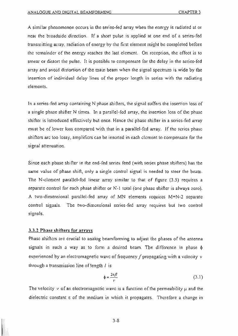
ANALOGUE AND DIGITAL BEAMFORMfNG CHAPTER 3
A similar phenomenon occurs in the series-fed array when the energy is radiated at or
near the broadside direction. If a short pulse is applied at one end of a series-fed
transmitting array, rad iation of energy by the first element might be completed before
the remainder of the energy reaches the last element. On reception, the effect is to
smear or distort the pulse. It is possible to compensate for the delay in the series-fed
array and avoid distortion of the main beam when the signal spectrum is wide by the
insertion of individual delay lines of the proper length in series with the radiating
elements.
In a series-fed array containing N phase shifters, the signal suffers the insertion loss of
a single phase shifter N times. In a parallel-fed array, the insertion loss of the phase
shifier is introduced effectively but once. Hence the phase shifter in a series-fed array
must be of lower loss compared with that in a parallel-fed array. If the series phase
shifters are too lossy, amplifiers can be inserted in each element to compensate for the
signal attenuation.
Since each phase shiner in the end-fed series feed (with series phase shifters) has the
same value of phase shift, only a single control signal is needed to steer the beam.
The N-element parallel-fed linear array similar to that of figure (3.5) requires a
separate control for each phase shiner or N-l total (one phase shifter is always zero).
A two-dimensional parallel-fed array of MN elements requtres M+N-2 separate
control signals. The two-dimensional series-fed array requires but two control
signals.
3.3.2 Phase shifters for arrays
Phase shifters are crucial to analog beamfonning to adjust the phases of the antenna
signals in such a way as to fonn a desired beam. The difference in phase $
experienced by an electromagnetic wave of frequency f propagating with a velocity v
through a transmission line of length I is
(3.1 )
The velocity v of an electromagnetic wave is a function of the penneability II and the
dielectric constant e of the medium in which it propagates. Therefore a change in
3-8

ANALOGUE AND DIGITAL BEAMFORMING CHAPTER)
phase can be obtained by a change in frequency, length of line, velocity of
propagation, permeability or dielectric constant.
Phase shifting devices can either be reciprocal or nonreciprocal. In the reciprocal
device, the phase change does not depend on the direction of propagation. On the
otherhand. a nonreciprocai phase shifter must have different control settings for
reception and transmission.
3.3.2.1 Selection criteria
There are currently two types of electronic phase shifters suitable for practical alTays:
the ferrite phase shifter and the semiconductor-diode phase shifter (discussed in
sections (3.3.2.2) and (3.3.2.3)). Selection of the type of phase shifter depends
strongly on the operating frequency and the RF power per phase shi fief. Above S
band (2 to 40Hz), waveguide ferrite phase shifters have less loss than diode phase
shifters. In situations in which RF powers are low and size and weight constraints
dictate a miniaturized design, diode phase shifters are preferred. Other factors that
have a bearing on the selection are listed below:
(a) Insertion loss: Insertion loss should be as low as possible. It results in a reduction
of generated power on transmit and of low signal-to-noise ratio on receive. It also
produces phase-shifter-heating problems.
(b) Switching times: The time to switch should be as short as possible. Tirnes on the
order of rnicroseconds are adequate for rnost applications.
(c) Drive power: Drive power should be as small as possible. A large arnount of
drive power generates heat and also may require power supplies that are too large
for a mobile system. Large drive power may also require expensive driver-circuit
components. Diode phase shifters require holding power as well as switching
power. Ferrite phase shifters can be latched i.e. they do not consume drive power
except when switching.
(d) Phase error: Phase error should be as small as possible. It should not reduce
anterma gain substantially or raise sidelobes in the radiation panem. One cause of
phase error is the size (in degrees) of the least significant bit of a digital phase
shifter. Other phase errors are due to manufacturing tolerances in the phase shifter
and driver.
3-9

ANALOGUE AND DIGITAL BEAMFORMING CHAPTER 3
(e) Transmitted power: The required power per phase shifter depends upon the
maximum range and the data rate of the system design.
(f) Physical size: The phase shifter should fit within a ")J2 by ')J2 cross section so that
it can be packaged behind each element. otherwise an expensive fan-out feed is
required.
(g) Weight: Phase shifter weight should be minimized In mobile and especially in
airborne or spacecraft, installations.
(h) Cost and manufacturing ease: For arrays with thousands of elements, the unit cost
must be low. Manufacturing tolerances must be as large as possible, consistent
with allowable system phase and amplitude errors.
3.3.2.2 Ferrite phase shifters
Construction of ferrite phase shifters fall into two categories: those phase shifters
enclosed by a waveguide structure and those built by using a microstrip configuration.
While the construction of the microstrip ferrite phase shifter is extremely simple, the
performance of the waveguide ferrite phase shifter is far superior, and is generally
used for most applications.
Ferrite phase shifters use ferromagnetic materials that include families of both ferrites
and garnets which are basically ceramic materials with magnetic properties. The
change in the applied dc magnetic fie ld of the ferrite produces a change in the
propagation properties because of a change in the permeability. which results in a
phase shift.
They may be analog or digital with either reciprocal or nonreciprocal characteristics.
Several types of ferrite phase shifters have been developed, but those that have been
of interest in applications are the toroidal, Reggia-Spencer and the faraday rotator
phase shifters. Since these phase shifters are enclosed by waveguide structures, their
manufacturing ease decreases, thus resulting in an increase in cost. Reference [33]
and [34] provides extensive infomlation on these ferrite phase shifters.
3-10

ANALOGUE AND DIGITAL BEAMFORMING CHAPTER 3
3.3.2.3 Diode phase shifters
The property of a semiconductor diode that is of interest in phase shifter design is that
its impedance can be varied with a change in bias control voltage. This allows the
diode to act as a switch. Phase shifters based on diode devices can be of relatively
high power and low loss, and can be switched rapidly from one phase state to another.
They are relatively insensitive to changes in temperature, they can operate with low
control power, and are compact in size. They are well suited to microwave integrated
circuit construction, and are capable of being used over the entire range of frequencies
of interest. However, their losses are generally less and their power handling is
generally higher at lower frequencies.
There are three basic methods for employing semiconductor diodes in digital phase
shifters, depending on the circuit used to obtain the individual phase bit. These are:
(a) the switched-line, (b) the hybrid-coupled and (c) the loaded line phase shifter.
(a) Switched-line phase shifter [331
A change in phase can be obtained by uti lizing one of a number of lengths of
transmission lines to approximate the desired value of phase. The various lengths of
line are inserted and removed by high-speed electronic switching.
There are at least two methods for switching lengths of transmission lines. These are
the parallel-line configuration and the series-line or cascaded configuration. Due to
the discrete nature of the digitally switched phase shifter, the exact value of required
phase shift cannot be achieved without a quantization error. However, this error can
be made as small as possible.
(i) Parallel-line configuration
Figure (3.6) illustrates the parallel-line configuration of the digitally swi tched phase
shifter in which the desired length is obtained by means of a pair of one-by-N
switches. Each of the boxes labelled S represents a single-pole single throw (SPST)
switch.
The N ports of each one-by-N switch are connected to N lines of different lengths 11•
12 •.. . , IN. The number of lines depends on the degree of phase quantization that can
be tolerated. This number is limited by the quality of the switches, as measured by
3-11

ANALOGUE AND DIGITAL BEAMFORMING CHAPTER 3
the difference between their impedance in the "off" and "on" positions. With many
switches in parallel, the "off' impedance of each must be high if the combined
impedance is to be large compared to the "on" impedance of a single switch. A
parallel line configuration with 16 lengths of line provides a phase quantization of
22.5' (± 11.25'), assuming the nth line is of length n1J16.
One-by-N switch One-by-N switch
Fig. 3.6: Digita lly switched pa rallel-line phase shi fter with N switchable lines
(from 1331)
A suitable form of switch is the semiconductor diode. The diodes anached to the ends
of the particular line selected are operated with forward bias to present a low
impedance. The remaining diodes attached to the unwanted lines are operated with
reverse-bias to present a high impedance. The switched lines can be any standard RF
transmission line. An advantage of the parallel-l ine configuration is that the signal
passes through only two switches and in principle, should therefore have lower
insertion loss than the cascaded or series line digitally switched phase shifter
described below. A disadvantage is the relatively large number of lines and switches
required when it is necessary to minimize the quantization error. The parallel-line
configuration has also been used when phase shifts greater than 21t radians are
needed, as in broadband devices that require true time delays rather than phase shift
which is limited to 21t radians.
(ii) Series-line (cascaded) configuration
The series-l ine (cascaded) digitally switched phase shifter (figure (3.7)) is more
commonly used than the parallel line confi guration. A cascaded digitally switched
phase shi fte r with four phase bits capable of switching in or out lengths of line equal
3-12

ANALOGUE AND DIGITAL BEAMFORMING CHA PTER 3
to }J16, A/8, 1J4 and ')J2 yie lds a phase shift with a quantization offJ l6, s imi lar to the
parallel-line shifter with 16 lengths of line described above.
0--0 0--0 r 1
U 9 ; ~ ~ ( f
U 0 )J16
"----J >VS
)J4
t Individual phase bit
Fig. 3.7: Cascaded four-bit digitallv switched phase shifter with )J16
guantization. Arrangement shown gives 135° (3 /8 wavelengths) phase shift
The binary quantization of line lengths make it convenient to apply digital techniques
fo r actuating the phase shifter (figure (3.8)).
Bit no. 4 Bit no. 3 Bit no. 2 Bil no. I
Input ... 1 0°, 22.5° H 0°,45° H 0°, 90° H 0°, 1800
Fig. 3.8: Schematic of a 4-bit phase shifter with IJ16 guantization
Output
•
Figure (3.7) shows a four-bit digital phase shifter consisting of four cascaded
modules. Each module consists of two single-pole double throw (SPDT) switches and
two line lengths for each bit. The minimum number of diodes per bit is four ( 16
diodes in total for a 4 bit phase shifter). It gives 16 steps in increments of 22.5°. The
SPOT switch in each module inserts either "zero" phase change or a phase change of
360/2n degrees, where n=l ,2,3,4_ When the upper two switches are open, the lower
two are closed, and vice-versa. Note that in the "zero" phase state, the phase shift is
generally not zero, but is some residual amowll $0' Thus the two states provide a
phase shift of $0 and $0+6.$. The difference 6.$ between the two states is the desired
phase shift required of the module.
(b) The hvbrid coupled phase shifter (reflection phase shifter) 133), 1351
Each module used in the series-line (cascaded) phase shifter can be replaced by a 3dB
hybrid junction. The hybrid-coupled phase bit, as shown in figure (3.9) uses a 3dB
3- 13

ANALOGUE AND DIGITAL BEAMFORM ING CHAPTER 3
hybrid junction with balanced reflecting terminations connected to the coupled arms.
Alternatively, a circulator could be used if a nonreciprocal phase shifter is desired.
Two switches (diodes) control the phase change.
Input ,_-7'-'0utPUI
x 4
3dB hybrid junction
Short circuits
Fig. 3.9: Hvbrid coupled phase bit (from 1331)
The 3dB hybrid has the property that a signal input at port 1 is divided equally in
power between ports 2 and 3. No energy appears at port 4. The diodes act to either
pass or reflect the signals. When the impedance of the diode is such as to pass the
signals, the signals will be reflected by the short circuits located farther down the
transmission line. The signals at ports 2 and 3, after reflection from either the diode
switches or the short circuits, combine at port 4. None of the reflected energy appears
at port 1.
The difference in path length with the diode switches open and closed is.6.1. The two
way path .6.1 is chosen to correspond to the desired increment of digitized phase shift.
A N bit phase shifter can be obtained by cascading N such hybrids. Moderately wide
bandwidths can be achieved with the hybrid coupled phase shifter.
(c) T he loaded-line phase shifter 1331, 1351
This phase shifter (figure (3.10» consists of a transmission line periodically loaded
with spaced, switched impedances or susceptances. Diodes are used 10 switch
between the two states of susceptances. The spacing between diodes is approximately
one-quarter wavelength at the operating frequency. Adjacent quarter-wavelength
spaced loading susceptances are equal and take either of two values.
3-14

r
ANA LOGUE AND DIGITAL BEAMFORMING CHAPTER ,
Input Output
Susceptances Diode switches
Fig. 3.1 0: Periodicallv loaded-line phase shifter (from 133D
I f the magnitude of the nonnalized susceptance is small , the reflection from any pair
of symmetrical susceptances can be made to cancel so that matched transmission will
result for either of the two susceptance conditions. Each pair of diodes spaced a
quarter-wavelength apart produces an increment of the des ired phase. The number of
pairs that are cascaded detennines the value of the transmission phase shift. To
achieve high-power capacity, many such sections with small phase increments can be
used so that there are many diodes to share the power. The ability to operate with
high power is the advantage of the loaded-line diode phase shifter. If the largest and
practical phase shift per diode pair is IJ l6 or 22.5°, 32 diodes are required to shift the
phase 360°.
The hybrid coupled phase shifter generally has lower loss than the other two (loaded
line and switched-l ine phase shifters) and uses the least number of diodes. It can be
made to operate over a wide band. The switched-line phase shifter uses more diodes
than the other types and has an undesirable phase-frequency response which can be
corrected at the expense of a higher insertion loss. This configuration is generally
restricted to true time-delay circuits and to low-power, miniaturized phase shifters
where loss is not a major consideration. For a four-bit phase shifter covering 360°,
the minimum number of diodes needed in the periodically loaded-line is 32, the
switched-line requires 16, and the hybrid-coupled circuit needs only 8. The
theoretical peak power capability of the switched-line is twice that of the hybrid
coupled circuit since voltage doubling is produced by the refl ection in the hybrid
circuit. The switched-line phase shifter has the greatest insertion loss, but its loss
3-15

ANALOGUE AND DIGITAL BEAMFORMfNG CHAPTER 3
does not vary with the amount of phase shift as it does in the other two types of
circuits.
3.3.3 Bandwidth of a rravs
The bandwidth of an alTay antenna depends upon the types of components, such as
radiators , phase shifters, and feed networks, comprising the array. The bandwidth is
also affected by many factors, including change of element input impedance with
frequency, change in array spacing in wavelengths that may allow grating lobes,
change in element beam width. etc.
In practice, most radiators for phased. arrays are matched over a broadband of
frequencies. Therefore, the radiator design is not a primary factor in the
detennination of bandwidth. The more severe limitation in bandwidth are detennined
by the frequency characteristics of the phase shifters and feed networks. In general,
the effects due to the phase shifters and feed nehvorks are additive, so that if the phase
shifter causes the beam to scan by an amount equal to 89p and the feed causes it to
scan by .19r, then the total beam scan is given by .19p + 69r.
3.3.3.1 Phase-shifter effects
To evaluate effects caused by the phase shifter alone, a corporate feed (equal-line
length parallel feed) is used to illWll inate all the radiator elements (see figure (3.11)).
The corporate parallel feed exhibits no feed effects since a signal at the input
illuminates all the radiating elements with the same phase regardless of frequency_
The bandwidth in this case is completely detennined by the type of phase shifter used
in the array. In this discussion, two basic types of phase shifters will be considered:
(a) time delay phase shifters (b) constant phase-type phase shifters.
3-16
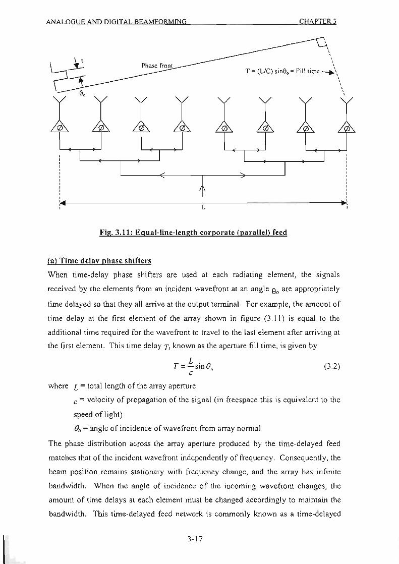
ANALOGUE AND DIGITAL BEAM FORMING
Phase front
CHAPTER 3
, , , , , , T '" (UC) sin90 Fill time -..\ , , , , , ,
, , , , , , , , , , , , , I" L
... :
Fig. 3.11: Equal-Hne-Iength corporate (parallel) feed
(a) Time delav phase shifters
When time-delay phase shifters are used at each radiating element, the signals
received by the elements from an incident wavefront at an angle 90 are appropriately
time de layed so that they all arrive at the output tenninal. For example, the amount of
time delay at the first element of the array shown in figure (3. 11 ) is equal to the
additional time required for the wave front to travel to the last element after arriving at
the first element. This time delay T. known as the aperture fill time, is given by
T=L sinlJ c '
(3.2)
where L = total length of the array aperture
c = velocity of propagation of the signal (in freespace this is equivalent to the
speed oflight)
Bo = angle of incidence of wavefront from array nonnal
The phase distribution across the array aperture produced by the time-delayed feed
matches that of the incident wavefront independently of frequency. Consequently, the
beam position remains stationary with frequency change, and the array has infinite
bandwidth. When the angle of incidence of the incoming wavefront changes, the
amount of time delays at each element must be changed accordingly to maintain the
bandwidth. This time-delayed feed network is commonly known as a time-delayed
3-17

ANALOGUE AND DIGITAL BEAMFORMING CHAPTER 3
beam-steering feed. The above discussion is valid for either a continuous wave (CW)
or a pulsed incidence signal. For the pulsed incidence signal, the time-delayed feed
preserves the shape of the pulse without any distortion.
Cb) Constant phase-type phase shifter
When constant phase-type phase shifters (phase shifters whose phase shift is
independent of carrier/centre frequency) are used at each element, the output phase
distribution of the feed matches that of the incident phase front only at one frequency
fo and for a particular incidence angle So. At a different frequency f t, the output phase
distribution of the feed network remains fixed, hence the array is phased to receive at
a difference incidence angle S t. The amount of beam squint with frequency is given
by the following relationship:
It sin 8] = 10 sin 80
or sin 81
= 10 sin 80 I ,
Figure (3. 12) shows this behavior.
(3.3)
75r---------------------------------,-----c---------~
60
i 45
t E • .!I 30 .
15
.. .. . ....
°O~~--------,~5----------30~--------~45~--------~60~--------~75 Beam angle 8t ceoter Irequency. dag
Fit!. 3.12: Beam angle shift with frequency (from 1321)
3-1 8

ANALOGUE AND DIGITAL BEAMFORMING CHAPTER 3
The beam peak angle is reduced for frequencies above the design frequency (fo) and
increased for frequencies below the design frequency. For a small change in
frequency, equation (3.3) shows that the change in scan angle is given by
(3.4)
The above expression shows the amount of beam squint depends upon the original
scan angle as well as on percent frequency change. At broadside (80 = 00), there is no
scanning regardless of the amount of change in frequency, and the array has infinite
bandwidth. When the beam scans away from broadside, the amount of beam squint
with frequency increases with scan angle. Therefore, the bandwidth of an array must
be specified in terms of the desired maximum scan angle. For most practical
applications, the desired maximum scan angle is ±60° from array broadside.
There is a direct relationship (equation (3.5)) between actual bandwidth and array size
[22].
LsinB, = 0.8868, (300) 1 !!.j"
where 4(M is the bandwidth in megahertz
L is the array length in meters
Bb is the beam broadening factor - chosen as unity for the unifonnly
illuminated array
(3.5)
Equation (3.5) shows that the bandwidth becomes smaller as the array is made larger
or as the scan angle is increased.
3.3.3.2 Feed effects
When a feed other than an equal-length parallel feed (corporate feed) is used, phase
errors due to the feed alone are produced across the array aperture. An example is the
end-fed series feed shown in figure (3.13).
3-19
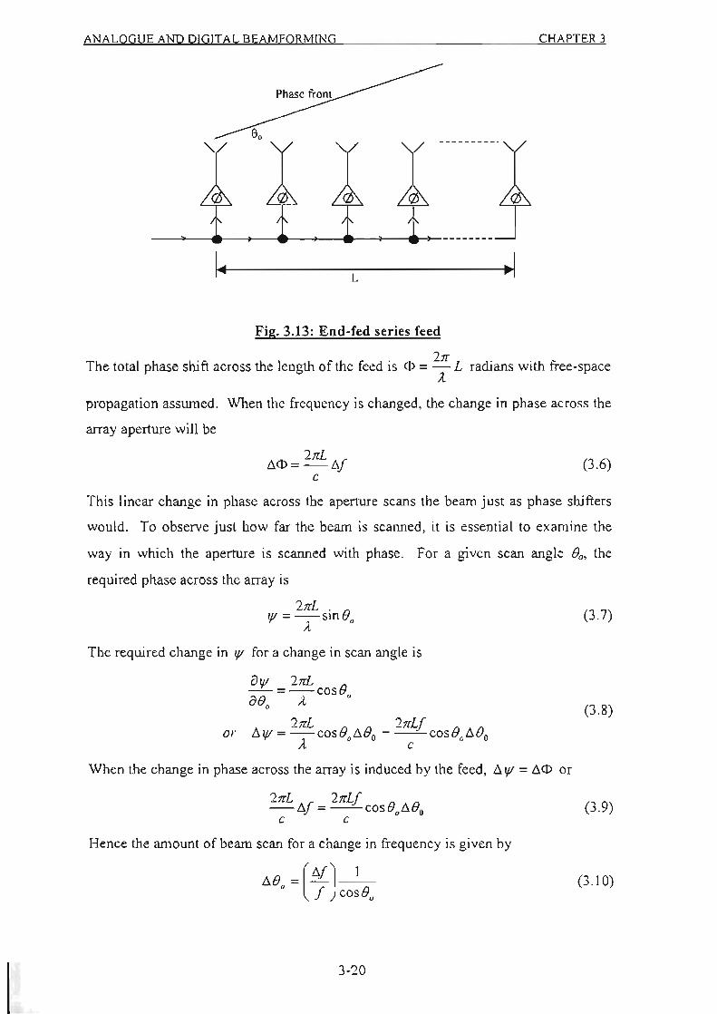
ANALOGUE AND DIGITAL BEAMFORM ING CHAPTER 3
eo
-~_>-__ -~-+----o _ ___ >- _______ _
I ~ L
Fig. 3.13: End-fed series feed
The total phase shift across the length of the feed is et> = 27f L radians with free-space A
propagation assumed. When the frequency is changed, the change in phase across the
array aperture will be
ilet> ~ 2!rL ilJ c
(3.6)
This linear change in phase across the aperture scans the beam just as phase shifters
would. To observe just how far the beam is scanned, it is essential to examine the
way in which the aperture is scanned with phase. For a given scan angle Bo, the
required phase across the array is
2!rL . () 'I/~--sm 0
A
The required change in 'If for a change in scan angle is
a'l/ 2!rL --~--cosB 80 A 0
o
2!rL 2!rLJ or fll{l = --cosBq6.Bo = --cos Bof1Bo A C
When the change in phase across the array is induced by the feed, f11f/ = 6.ct> or
2!rL ilJ ~ 2!rLJ COS (}oil(). C C
Hence the amount of beam scan for a change in frequency is given by
M) ~ (ilJJ 1 o / cos BD
3-20
(3.7)
(3.8)
(3.9)
(3.10)

ANALOG UE AND DIGITAL BEAMFORMING CHAPTER 3
For a 600 scan angle, the scanning caused by the feed alone is slightly greater than
that caused by the aperture. Therefore, the bandwidth of the series feed is essentially
half of that of the equal-line-length parallel feed (corporate feed).
3.4 Digital beamforming
Digital beamforming (OBF) for signal reception is conceptually simple. Each antenna
element in the array is connected to a pre-amplifier (LNA) and then to an AID
converter, as shown in figure (3.14).
Antenna 1
LNA
Antenna N
LNA
AID and coder
AID and coder
Digital data bus
Digital Beamforming
processor
Fig. 3.14: Digital topology
Output
The outputs of the AIDs are connected to a digital data bus. A DBF processor can
then manipulate this data to form any number of multiple beams, perform rapid beam
scan, produce low-side lobe beams and perform adaptive nulling.
Because the element combining algorithms can be formulated in true time delay fonll ,
there are no bandwidth limitations in the digital beamformer. The serious limitation is
the bit-bandwidth product of the AID. The sampling rates and resolutions (number of
bits) provided by present-day (June 2000) AID converters cover a wide rage of values.
Invariably. a balance between these two parameters must be sought because it is
difficult to achieve both a high sampling rate and a high resolution. In CDMA
system s, 4 to 6 bit AIDs have been noted to provide adequate performance [36]. At
the present time, AID hardware appears suitable only for low microwave frequencies
and below. Table (3.1) lists the resolution and sampling rates of the state-of-the-art
ADC technology ([37]-[43]).
3-21

ANALOGUE AND DIGITAL BEAMFORMING
e lSS
ucourant et a . rysta emlcon uctor
a
a e . : er ormance 0 state-o -t e-art
.ts
5 reporte ID
CHAPTER 3
z
z z z z
z z z
These ADCs were cited as state-of-the-art in [17] as at 1996. It should be pointed out
that very few of the converters are commercially available. As pointed out in [44],
commercially available ADCs are the result of market demand rather than technology
enhancement. Currently, commercially available products range from 8bit, 80MHz to
IQ bit, 200MHz, by Texas Instruments and Analog Devices, respectively. Advances
in superconducting ADCs are promising, hut commercial realization of this hardware
IS years away.
The processor used in an all -digital beam forming array has two speed regimes: the
handling of digitized RF requires coherent beam formation at the AID converter upper
frequency, while the calculation and change of amplitude and phase tapers for
sidelobe control, etc., can proceed at a much slower rate. That is, the RF data
handling requires a very fast processor while for the array control functions a much
slower processor will suffice. Beam-formation and tracking of mobiles depends on
the speed of the mobiles. The mobiles need to tracked by beams when moving from
one cell to another. It is intuitive from the contrast in speed of the mobile and
digitized RF data, that a much slower processor be required for array control functions
than that for RF data handling. Some array functions such as adaptive nulling, may
require a specialized and/or separate processor for such tasks as matrix inversion,
singular value decomposition, etc. All of the digital hardware and software is
avai lable, only the AID capability is awaited.
The above digital topology describes a straight-forward approach that digitizes the
input signal directly and processes the digitized data to extract the needed
information. Clearly, an all-digital adaptive array is currently impractical given the
usually high operating frequencies that are part of real communication systems.
3-22

ANALOGUE AND DIGITAL BEAMFORMINQ CHAPTER 3
One compromise is to down-convert the microwavelRF input signals to IF. The
digitizing is then performed on the IF signals . The main component of the down
conversion process is the multiplication device or mixer which would probably
remain analog for a long time to come. It should also be noted, even if the incoming
signal is down-converted in frequency, its allocated bandwidth could be too wide to
be handled digitally.
The performance of a digital beamforming (DBF) receiving array is. to a large extent,
determined by the capabi lities of the receivers that are used at the antenna elements.
The receivers perform the functions of frequency conversion, fi ltering, and
amplification of the signal to a power level that is commensurate with the input
requirements of the AID converters or with the output power requirements. Since the
elemental receivers are a significant factor in determining the cost of a DBF antenna,
it is important when designing receivers to adopt an architecture that leads to
rece ivers that are low in cost and yet meet performance requirements.
3.4.1 Receivers for digital beamforming
3.4.1.1 Single-channel receiver
A basic down-conversion receiver scheme is shown in figure (3.15).
RF input signal,------,
Bandpass filter
Mixer IF Amplifier
,-----,
Fig. 3.15; A basic single-channel receiver
Digital processor
A fil ter is used at the input fo r image suppression. Following the filter is a mixer that
converts the input signals into an IF. An IF amplifier is used to amplify the input
signals to a proper level to be digitized by the AID converter. After the AID converter
a digital memory unit is used to store the informat ion for further processing. The
memory unit and digital processor may be combined in a single un it.
To fulfil the Nyquist criterion, the AID converter must operate at more than twice the
frequency of the upper IF range (the IF ampli fier has a bandwidth from DC to its
3-23

ANALOGUE AND DIGITAL BEAMFORMING CHAPTER 3
upper frequency limit. If the low-pass cut-off frequency of the IF amplifier is
infinite ly sharp, the sampling rate can be at the Nyquist criterion. However, this cut
off frequency response has some finite slope, thus, the sampling rate must be higher
than the Nyquist rate (approximately 2.5 to 3 times the input bandwidth). Two
undesirable aspects should be considered for this down-conversion approach [30]:
spurious output and image problems. A frequency mixer used to down-convert an
input signal to a proper IF range is usually considered as a linear device, but strictly
speaking, it is a non-linear device. The spurious output or harmonics are filtered out
by the low-pass filtering effect of the IF amplifier at the output of the mixer. The
image frequencies entering the IF passband can be filtered out with a RF bandpass
filter at the input to limit the input bandwidth.
3.4.1.2 Two-channel receiver
Another approach to building a digital receiver extends the basic down-conversion
idea to a two-channel approach: an in-phased channel-I; and 90° out-of-phased
channel-Q [30] . The basic structure of this receiver is shown in figure (3. 16).
RF input signal , -----,
Bandpass filter
Power divider
Mixer IF Amplirfi",er,---,
ND Memory and
digital processor
Fig. 3.16: A two channel digital receiver: in-phase input and out-of-phase local
oscillator (from 130))
The input signals pass through a bandpass filter and an in-phase power divider that
divides the input into two parallel channels. Two mixers are used to down-convert
the input signals into two IF channels. The two mixers are fed by one local oscillator.
3-24
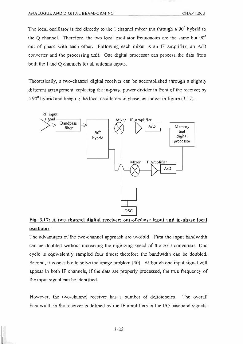
ANALOGUE AND DIGITAL BEAMFORMING CHAPTER 3
The local oscillator is fed directly to the I channel mixer but through a 90° hybrid to
the Q channel. Therefore, the two local oscillator frequencies are the same but 90°
out of phase with each other. Following each mixer is an IF amplifier, an N D
converter and the processing unit. One digital processor can process the data from
both the I and Q channels for all antenna inputs.
Theoretically, a two-channel digital receiver can be accomplished through a slightly
different arrangement: replacing the in-phase power divider in front of the receiver by
a 90° hybrid and keeping the local oscillators in phase, as shown in figure (3. 17).
RF input signal,----,
Bandpass filter
90' hybrid
Memory and
digital processor
Fig. 3.17: A two-channel digital receiver: out-or-phase input and in-phase local
oscillator
The advantages of the two-channel approach are twofold. First the input bandwidth
can be doubled without increasing the digitizing speed of the NO converters. One
cycle is equivalently sampled four times; therefore the bandwidth can be doubled.
Second, it is possible to solve the image problem [30]. Although one input signal will
appear in both IF channels, jf the data are properly processed, the true frequency of
the input signal can be identified.
However, the two-channel receiver has a number of deficiencies. The overall
bandwidth in the receiver is defined by the IF amplifiers in the I/Q baseband signals .
3-25

ANALOGUE AND DIGITAL BEAMFORMING CHAPTER 3
Because of the way in which the I and Q signals are derived, they may suffer from the
followi ng performance limitations [17]:
(i) There may be a poor match between the characteristics of the I and Q signals over
the receiver bandwidth.
(ii) The I and Q channels may not maintain phase quadrature over the receiver
bandwidth.
(iii) The I and Q channels may have separate dc offsets. In baseband sampling, dc
offsets occur at the output of the I and Q mixers when the RF frequency is equal to the
local oscillator frequency but with a phase difference. The I and Q dc offsets are
different, since no two mixers are perfect ly identical.
(iv) Nonlinearities of the components used in the I and Q channels may produce . .
spunous nOIse.
A major drawback of the two-channel approach is its cost of implementation due to
the fact that each antenna input requires two sets of mixers, IF amplifiers and AIDs
(for both the I and Q channel).
3.4.1.3 Direct sampling receiver
The amplitude matching and the phase orthogonality of the I and Q channels are
extremely critical. This has created interest in an alternative conversion teclmique
(figure (3.18)), in which the signal is sampled and digiti zed at IF and the VQ signal is
generated digitally.
RF input signal,-___ -,
Bandpass filter
LNA Mixer
Bandpass filter
Fig. 3.1 8: Direct sampling receiver (from 11 7D
Digital UQ generation
In this receiver, the I and Q outputs are formed using a digital filter, thereby
eliminating I and Q matching problems from the channel. This approach eliminates
the need for two sets of mixers, IF ampl ifiers and AIDs at the expense of one faster
AID and some additional digital circuitry. The bandpass filte r at the input is used to
eliminate out-of-band interference. This band pass filter can be placed before or after
3-26

ANALOGUE AND DIGITAL BEAMFORMING CHAPTER 3
the low-noise amplifier (LNA) with different consequences. By placing the filter
before the LNA, the highest dynamic range (at the expense of a higher system noise
figure) can be achieved, whereas by placing the filter after the LNA, the maximum
receiver sensitivity can be obtained. A low-noise amplifier is essential since it
establishes the system noise figure.
There are two methods for carrying out the direct sampling: Nyquist sampling and
down-sampling (also called direct down-conversion). The Nyquist sampling theorem
[or sampling a bandpass analog signal (a signal having no frequency components
above a certain frequency fmax) requires that the sampling rate be at least two times the
highest frequency component of the analog signal (i.e. 2fmaJ. For an RF signal with a
bandwidth 8 centred at fRF' the sampling rate must then be 2(fRF + 812) where the
highest frequency component in the signal fmax is given by fmax= fRF + 8 12. It is
possible to use sampling rates lower than 2fma;.; and still get an exact reconstruction of
the information contained in the analog signaL This approach is referred to as direct
down-conversion. It allows AIDs with slower sampling rates to be used in
applications where performance, power consumption, and cost are critical. For a
bandpass signal with bandwidth B, the minimum sampling rate for infonnation
extraction is two times the bandwidth B. References [45] and [46] derive the
constraints for a band pass signal using down-sampling. To ensure that spectral
overlap does not occur, the sampling frequency Is must satisfy [46]
I s;2B( k -I) s N -I
(3.11 )
and
Is ;'2B(~) (3. 12)
in which k = [maxlB and k ~ N since Is ~ 2B· For example, in order to digitize a RF
signal (directly) with bandwidth of 4MHz centred at 2GHz, application of equations
(3.11) and (3.12) with k ~ 500.5, yields sampling frequencies in the range from 8MHz
(twice the bandwidth) to 4.004GHz (Nyquist sampling rate) for integer values
N::S;; 500.5. At first glance, it seems possible to use down-sampling at the 2GHz RF
frequency at a rate of twice the signal bandwidth, thus eliminating the need for
frequency downconversion. However, there is a practical limitation: the ADC must
still be able to operate on the highest frequency component in the signal (fRF + BI2).
3-27
ANALOGUE AND DIGITAL BEAMFORMING CHAPTER}
This is usually specified as the analog input bandwidth for the ADC. Also,
conventional ADCs are designed such that their sampling rates are twice that of the
maximum input frequency i.e. designed for Nyquist sampling. Perfonnance of ADCs
typically degrades with increasing input frequencies. Down-sampling also introduces
another problem: a reduction in sampling rate results in a decrease in the width of the
guard band, thus causing a filtering problem. Stringent requirements for analog
bandpass filters (e.g. steep ro11offs) are needed to prevent distortion of the desired
signal from unwanted adjacent frequency components. Furthennore. an IF down
conversion stage may be required fo r effective down-sampling. The sampling jitter
requirements of the sampler must also be high to ensure that the carrier frequency is
accurately sampled to recover the signal phase infonnation that is required for PSK
demodulation.
In order to carry out the coherent phase detection necessary for generating the digital I
and Q signals, a digital down-converter (DDC) is used. A DDC contains a
synthesizer, a quadrature pair of digital multipliers (which act as mixers in the digital
domain) and some filters that implement both low-pass filtering and decimation [17] .
It extracts a narrowband signal from a wideband digital input and decimates it to a
reduced data rate. Since the new data rate is proportional to the bandwidth, all of the
infonnation in the digital signal has been captured without excess bandwidth being
carried by the digital signal. A benefit derived from the reduced data rate is that the
digital signal processor (OSP) (following the DOe) is better able to cope with it.
Digital downconversion not only eliminates the need for another IF stage but it also
overcomes many of the problems related to analog downconversion and lowpass
digitization. Digital downconversion can also be perfonned by this same DSP.
Alternatively, stand-alone DDCs can be used. However, by relieving the DSP from
the processing burden associated with the digital downconversion functions, more
computational power becomes avai lable for the tasks required for array processing
(updating of adaptive beamfomling weights, etc).
The direct sampling receiver architecture is very attractive from a cost point of view.
Also because of its potentially superior technical perfonnance, it suitable for high
perfonnance DBF system applications.
3-28

ANALOGUE AND DIGITAL BEAMFORMJNG CHAPTER 3
3.5 Adaptive beamforming in CDMA
The use of an adaptive array in a communication system requires some degree of
compatibility between the signalling waveforms and the adaptive array. There are
several reasons for this [47]:
(a) The adaptive weights are random processes, and they modulate the desired signal.
The desired signal must be chosen so this modulation does not destroy the
effectiveness of the communication system.
(b) There must be some difference between the desired signal and the interference
waveforms, so these signals can be distinguished in the array.
(c) There must be some method for reference-signal generation and for acquiring
system timing or frequency when the array is in the system.
Adaptive beamforming for CDMA wireless communications has been drawing more
and more attention from both the communications and antenna communities [47J.
Adaptive beamforming is highly suitable for a CDMA system, because the spreading
codes can be used as a reference for beam forming.
3.5.1 Reference signal acq uisition
An important function performed by the digital processor in the previously mentioned
receiver configurations is that of adapt ive beamfonning. There are a number of
criteria and algorithms for adaptive beamfonning [17J. They all require some sort of
reference signal in their adaptive optimization process. Reference signal refers to a
priori and explicit information about the signals of interest . Explicit reference can be
divided into two categories: spatial reference and temporal reference. Spatial
reference is mainly referred to as the angle-of- arrival (AOA) in fomlation of a desired
signal. A temporal reference signal may be a pi lot signal that is correlated with the
desired signal, a pseudo-noise (PN) code in the case of a COMA system. The form of
avai lable reference depends on the particular system where adaptive bearnforming is
to be implemented. If an explicit reference signal is available in a system, it should be
used as much as possible for less complexity, high accuracy and fast convergence.
Adaptive beam forming is highly suitable for a COMA system, because the spreading
codes can be used as a reference for beam forming. The common implementation of
adaptive beamfonn ing in a COMA wireless communication system is the use of
3-29
ANALOGUE AND DIGITAl BEAMFORMING CHAPTER 3
Campton's reference generation loop [47]. A generic implementation configuration
for adaptive beamfonning in a CDMA wire less communication system is shown in
figure (3.19).
w
S Array output
+ Adaptive processor Error
signal
r--""I~~:""j--__ T_,.'Data
CDMA Code
Limiter
Fig. 3.19: Configuration for adaptive beamforming in CD MA (from 1471)
In this configuration, the demodulation is carried out after beamforming. The array
output S is first mixed with a COMA-coded local oscillator signal, which is filtered
and limited. The limited signal is re-modulated by mixing with the corresponding
COMA coded local osci llator signal. The re-modulated signal is used as the refe rence
signal, which is compared with the delayed array output to produce an error signal.
The error signal drives the adaptive processor to update the beamforming weights.
This feedback loop is nonlinear due to the limiter operation.
The output of the 151 mixer contains both desired and interference components. These
interference components are mainly muitiuser interference i.e. the signals of undesired
users. Some channel and receiver noise are also present. Because the CDMA code
modulation matches that on the desired signal, the desired signal component at the I SI
mixer output is compressed to data bandwidth, while the interference is not. The filter
bandwidth is chosen wide enough to pass the desired signal, which now has only data
modulation, but not wide enough to pass the interference, which has full -code
bandwidth. As a result, the fil ter removes all but the centre portion of the interference
spectrum. The signal is passed through a limiter, which controls the amplitude of the
reference signal. The desired signal passes through this loop unchanged, except for
the amplitude adjustment at the limiter and the envelope time delay associated with
the filter.
3-30
ANALOGUE AND DIGITAL BEAMFORMING CHAPTER 3
An interference signal without the proper PN-code modulation, however has its
waveform drastically altered by this loop. For example, a CW interfering signal
which has a single line spectrum at the array output produces a reference signal with
the full-bandwidth of the PN-code modulation (and with lower power than at the array
array output). The correlation between the interference signal at the array output and
the reference signal has been essentially destroyed by the loop.
There are several reasons why the reference signal amplitude must he controlled [47]:
(a) The amplitude of the reference signal determines the amplitude of the signals
present at the array output, which should fall within a certain range for proper
operation of the multipliers, etc., in the feedback loops.
(b) The reference-signal amplitude should be fixed so that the array will yield a
maximum ratio of signal power to interference and noise power at the output.
(c) The reference-signal amplitude cannot be linearly dependent on the array output
amplitude, because then there is a problem with the operation of the array
weights. For example, if the reference loop were linear and its gain (to the desired
signal) were greater than unity, the loop will return a reference signal larger than
the array output signal, causing the array weights to increase without limit.
Conversely, a loop gain less than unity returns a reference signal smaller than the
array output, causing the array weights to drop to zero. Thus stable operation
requires a fixed reference-signal amplitude.
(d) When the reference-signal amplitude is fixed, the desired signal voltage at the
array output will also be fixed, regardless of the incident power of the desired
signal. This behavior is important for the delay-lock loop [47] used for track code
timing; it makes the threshold setting for code acquisition independent of
incoming signal strength.
The processing loop in figure (3.19) not only generates the reference signal, but also
delivers the desired signal with the PN-code removed at the output of the data
bandwidth filter. The desired signal is available at this point once the interference has
been nulled. Thus, the reference-signal loop incorporates spectrum despreading. This
configuration is also compatible to an asyncronous uplink CDMA system where
despreading is done after beamfomling [17]. It should be noted that this reference
loop only operates properly as long as the local PN code is timed properly with
3-31

ANALOGUE AND DIGITAL BEAMFORMING CHAPTER 3
respect to the code on the desired incoming signal. This timing or synchronization is
accomplished by a delay-lock loop. References [47] and [48] describe a novel delay
lock tracking loop that is designed to lock and track in the presence of data
modulation on the desired signal, a feature that is only possible with an adaptive array
in front of the loop. This adaptive array system is thus able to automatically lock on
and track a desired signal with the correct code, while a signal with the incorrect code
or no code at all is rejected.
3.5.2 Implementation issues for CDMA adaptive beamforming
Due to the fact that each CDMA user would require a separate loop, it would be cost
effective in a multiuser system to implement this loop in software in baseband.
The loop can also be implemented at IF usmg hardware followed by digital
processing. This setup not only places increased requirements on the digital processor
(which now has to process a much higher frequency signal), but is also costly in a
multiuser system where hardware would be required for each user. The loop cannot
he processed at RF (digital technology at RP is awaited). Although analogue
beamforming and loop implementation (using hardware) can be performed at RF, the
RF error signal would not be able to be processed by a present-day adaptive
processor. Hence RF adaptive beam fanning of the above loop is presently
impossible. However, the weights themselves can be implemented in hardware using
analog phase shifters and attenuators at either RF (following the antenna elements) or
rF (following the IF amplifiers). The processing of the weights in this case can be
performed at basebandlIF. In a large array, this setup is costly and increases the
complexity of the front-end. The best alternative is to perform adaptive beamfonning
at baseband with the weights being implemented digitally in software.
3-32
ANALOGUE AND DIGITAL BEAMFORM1NG CHAPTER 3
3.6 Synopsis of some implemented adaptive array systems
This section provides a brief description/study of some adaptive antenna systems and
the advantages and disadvantages of their implementation trends.
Reference [49] focuses on the stability problem that exists in adaptive antenna arrays
when the weighting functions operate at a nonzero frequency. This paper shows how
stability can be achieved by a simple time-compensation procedure. As a result. the
weight processor can be implemented digitally. Nonzero frequency weighting in
adaptive antenna arrays was introduced as a means to overcome some drawbacks
encountered during implementation of conventional arrays whose weights operate
around dc. Some of these drawbacks are dc offsets, feed through component
imbalance. etc, and are usually associated with analog devices. The paper also cites
an implementation of a four-element adaptive array with weights at an IF of 41 OMHz.
Perfonnance improvement in interference rejection over the conventional baseband
array is also demonstrated. Also cited, is an array whose weight processor is
implemented entirely with analog components. As a result, precise adjustments are
difficult to achieve due to drifts and nonlinearity effects. Furthennore, analog
integrators in adaptive processors suffer from imprecision, have a voltage limitation,
and face an uncertain storage of infonnation. This study was initially prompted by
the desire to design the nonzero frequency weight processor by digital means in order
to make this storage digital , and hence improve upon the analog integration.
Reference [50] discusses a phase-locked HF (30MHz) receiving array using separate
RF amplifiers for each element (6 elements in total). The signals from each element
are combined at an intennediate frequency of 3. 7MHz. The type of array considered
corrects essentially all phase errors between the distant transmitter and the point
where the received signals are combined. This includes errors due to the propagation
path, array element motion, near-field obstructions, and instabilities in electronic
equipment and RF cables. The array also corrects phase shifts due to changes in angle
of arrival, thus giving it the highly desirable property of automatically tracking a
desired signal.
3·33
ANALOGUE AND DIGITAL BEAMFORMrNG CHAPTER 3
An adaptive antenna for a TDMA mobile telephony system is described in [51]. The
adaptive array operates at a centre frequency of 172 1MHz and consists of 10 elements
arranged in a circular configuration. The weighting and summing of the received
signals are performed on the received RF signal allowing the use of an ord inary base
station as a receiver. The weighting is performed on the received RF signal using a
phase shifter and an attenuator. The phase shifter accuracy is 1 degree and the
attenuator is adjustable in I dB steps down to - 50dB. The RF signal is split and
down-converted to the baseband and separated into I and Q channels where sampling
at bit rate is done (270kHz). The ADC used has an 8 bit resolution with a dynamic
range from - 32dBm (O.63J~W) to - 80dBm (JOpW). Digital signal processing is
thereafter employed.
Reference [52] discusses an adaptive antenna for CDMA cellular systems. The
performance of the adaptive antenna in various scenarios has been studied. There are
four antenna elements in the array and the modulation scheme is QPSK. A processing
gain of 128 was used. The spread spectrum signal received by the antenna elements is
first processed by a weighting summing circuit. The output is then fed into two
branches, one for symbol detection using a rake receiver and the other for comparing
with the reference signal. The advantage of this scheme is that only one Rake receiver
is needed and the path searcher operates in an environment of high signal to
interference ratio (SIR) once an appropriate beam is formed. In a real system. the
pilot signal can be used as part of the reference signal, but in the work reported in this
paper, the antenna array is operated in a decision directed mode which means that the
reference signal is obtained by respreading the detected symbols with phase and
amplitude adj ustment .
In [53], a new type of adaptive antenna is presented, which is intended for use in
mobile receivers. A nonlinear, adaptive, analog feedback controller has been
developed to control the phase relationship between two receiving elements. Both the
contro ller andRF prototype are described in this paper. The prototype system
described in this paper would be noteworthy for several reasons: First, the antenna
diversity does not come at the price of additional expensive RF parts. This is in
contrast to the multiple antenna systems that do the combining in baseband
3-34

ANALOGUE AND DIGITAL BEAMFORMTNG CHAPTER)
processing, which requires that each antenna have its own LNA and mixer. Tt is
common in modern spatial diversity systems to perform a down-conversion on each
antenna signal before processing. The signals are digitized, then the computational
power of a DSP is brought to bear on the problem of inteJJjgent combining. This
approach to building spatial diversity systems can be expensive; each new diversity
branch requires its own LNA, mixer and ADC. However, the prototype system in
[53] is much more cost effective. Second, the adaptive antenna would be completely
modular, essentially a stand-alone "smart" antenna. The command level voltage
could either be derived from the IFlbaseband block or be simple, fixed reference.
Third, the command level essentially sets the level of the automatic gain control at the
receiving antenna, which relaxes the linearity requirement of the LNA. Finally, the
non linear, analog controller proposed is a novel design and for this application, more
cost efficient than traditional microprocessor-driven approaches.
From the above discussion, it is evident that antenna diversity comes at the expense of
additional expensive RF parts (LNA, mixer and ADC). These systems are also very
complex and expensive due to the large number of receivers required. They also
require accurate calibration procedures for the phase and amplitude mismatches
between channels. In [54] a multichannel measurement system using a single receiver
is described. The system is based on a complex wideband radio channel sounder and
a fast RF switch. The carrier frequency of the sounder is 2.154GHz and the
bandwidth is lOOMHz. The system provides real-time recording of signals from
multiple input channels and this enables real dynamic array measurements of the radio
channel of a moving mobile. The continuously recorded path lengths can be over one
hundred metres. This method simulates a real adaptive array and therefore gives a
realistic picture of the operation of practical adaptive array radio systems. In order to
measure multiple antenna elements with a single receiver, a fast RF switching unit is
required behind the antenna. The switching unit is based on a TTL-controlled GaAs
switch with a switching time of 3ns. The system used in this paper has 8 channels.
The worldwide cellular and PCS infrastructure build-out has provided market
incentives to develop better radio receivers. Better means smaller, lower power
dissipation, high sensitivity, less factory tweaking, high manufacturing yields, field
programmability, and operational flexible. Reference [55] discusses a new chipset
3-35

ANALOGUE AND DIGITAL BEAMFORMING CHAPTER ]
that has been developed that can be used to design high sensitivity, lower power
digital receivers for a variety of cellular and PCS standards, including AMPS, IS-1 36,
PDC, GSM and CDMA. One of them, the AD6600 is a dual channel, gain ranging
receIver ADC that can sample IF signals from 70MHz to 250MHz at 20 mega
samples per second (MSPS). It has on chip peak detectors, and received signal
strength indicator (RSSI). It also has two analog input pins that can be used to sample
separate diversity antennas. At the rated iF frequenci es, 90dB of dynamic range is
achieved: 30dB from the gain ranging and 60dB from the 11 bit ADC. The other
chip, the AD6620 is a dual channel digital decimation programmable filter designed
to interface di rectly with the AD6600 and subsequent DSPs. This chip can accept 16
bit input words at up to 65MSPS; the decimated data can be accessed by serial or
parallel words. The combination of high IF over-sampling with programmable digital
filtering allows designers to replace many analogIRF functions with digital functions.
Due to the difference in application (centre frequency, bandwidth, technology, etc.) , a
performance comparison of the above systems cannot be made.
3-36

COMA CONCEPTS CHAPTER 4
CHAPTER 4
CDMA CONCEPTS
4.1 Introduction
In chapter 3, an adaptive beamfonning scheme for CDMA using Compton's loop was
described. It was assumed that the reader was familiar with CDMA theory. This
chapter provides a comprehensive overview on CDMA. This theory is reinforced by
simulation work using Advanced Design System (ADS) software [7]. This chapter
forms the basis for the simulation models utilized in the following chapters. The list
of references for CDMA is exhaustive. However, the reader is referred to [I], [56],
[57] and [58] for further reading.
CDMA (Code Division Multiple Access) is a form of spread spectrum. instead of
using frequencies or time slots as in FDMA and TDMA technologies, it uses codes to
transmit and distinguish between multiple users. Because the users are distinguished
by codes, many users can share the same bandwidth simultaneously. This universal
frequency reuse is crucial to CDMA's distinguishing high spectral efficiency. As a
result CDMA has gained international acceptance by cellular radio system operators
as an upgrade from current technologies. CDMA systems provide operators and
subscribers with significant advantages over analog and conventional TDMA-based
systems. Some of the advantages of CD MA are as follows:
• Increased capacity
• Improved voice quality, eliminating the audible effects of multi path fading
• Enhanced privacy and security
• improved coverage characteristic which reduce the number of cell sites
• Simplified system planning reducing deployment and operating costs
• Reduced average transmitted power, thus increasing talk time for portable devices
• Reduction in the number of calls dropped due to handoff failures
• Development of a reliable transport mechanism for wireless data communications
4·1
COMA CONCEPTS CHAPTER 4
• Coexistence with previous technologies due to CDMA and analog multiple access
protocols operating in two spectras with no interference.
4.2 Background
To understand why there is a demand for CDMA, it is necessary to know the
background behind previous spread spectrum systems. Spread spectrum
communications have been used for encrypting military communications for many
years. Its strength in the military arena lie in its ability to resist enemy jamming and
to provide secure communications. It is difficult to interfere with or intercept a
CDMA signal because of its use of a spread signal. The great attraction of CDMA
technology from the beginning was its inherent ability to boost communications
capacity and reuse frequencies to a degree unheard of in narrowband multiple access
wireless technology. Its civilian mobile radio application was proposed theoretically
in the late 1940's, but its practical application in the market did not take place until 40
years later due to the many technical obstacles that still needed to be overcome.
However, the rapid development of high density digital integrated circuits (lCs),
combined with the realization that regulating all transmitter powers to the lowest level
required for a link would achieve optimal multiple access communication, allowed
CDMA to materialize as a working technology. In 1991 , promising results of the first
field trials demonstrated that CDMA could work as well in practice as it did in theory.
Commercial CDMA was introduced, tested, standardized. and initially deployed in
less than seven years. This is a relatively rapid maturation cycle compared to other
technologies such as TDMA. The first commercial CDMA service was launched in
Hong Kong in 1995, followed by a launch in Korea and Pennsylvania. It has rapidly
become the primary choice of carriers in the United States.
4.3 Comparison between FDMA, TDMA and CDMA
FDMA (Frequency Division Mult iple Access), TDMA (Time Division Multiple
Access) and CD MA are the three basic multiple access schemes.
FDMA divides radio channels into a range of radio frequencies and is used in
traditional analog cellular systems. With FDMA utilizing a single carrier per channel
(SCPC), only one subscriber is assigned to a channel at a time. Other users can access
4-2

CDMA CONCEPTS CHAPTER 4
this channel only after the subscriber 's call has terminated or after the original call is
handed off to a different channel by the system. FDMA cellular standards include
AMPS (Advanced Mobile Phone Service) and TACS (Total Access Communications
System).
TDMA is a common mUltiple access technique employed in digital cellular systems.
It divides radio channel into time slots to obtain higher capacity. Its standards include
North American Digital cellular (NADC), Global System for Mobile communication
(GSM) and Personal Digital Cellular (PDC). As with FDMA, no other user can
access an occupied TDMA channel until the channel is vacated.
CDMA uses a radically different approach. As mentioned earlier. it assigns a unique
code to each subscriber to put multiple users on the same wideband channel at the
same time. The codes, called "pseudo-noise (PN) code sequences", are used by both
the mobile and the base station to distinguish between users. The IS-95 COMA
standard was adopted by the TtA (Telecommunications Industry Association) and
became a digital cellular standard in 1992. The J-STD-008 standard for personal
communication systems (peS) was also accepted by ANSI (American National
Standards Institute). CDMA is the first digital technology which meets the exact
standards of the CTIA (Cellular Telecommunications Industry Association) [1].
Depending on the mobility of the system, CDMA provides 10 to 20 times the capacity
of AMPS, and 4 to 7 times the capacity of TDMA. COMA is the only one of the
three technologies that can efficiently utilize spectrum allocation and offer service to
many subscribers without requiring extensive frequency planning. All CDMA users
can share the same frequency channel because their conversations are distinguished
only by a digital code, while TDMA operators have to coordinate the allocation of
channels in each cell in order to avoid interfering with adjacent channels. The
average transmitted power required by COMA is much lower than that required by
analog, FDMA and TDMA technologies.
4-4 Spreading the spectrum
Spread spectrum multiple access transmits the entire signal over a bandwidth that is
much greater than that required for standard nalTowband transmissions in order to
4-3

CDMA CONCEPTS CHAPTER 4
gain signal-to-noise (SIN) performance. In channels with narrowband nOIse,
increasing the transmitted signal bandwidth results in an increased probability that the
received information will be correct. Because each signal is a compilation of many
smaller signals at the fundamental frequency and its harmonics. increasing the
bandwidth results in a more accurate reconstruction of the original signal. The
effective drawback of narrowband data communications is the limitation of
bandwidth. Thus signals must be transmitted with enough power so the corruption by
gaussian noise is not as effective and the probability that the data received is correct
will remain low. This means that the effective SIN must be high enough so that the
receiver can recover the transmitted code without error.
From a system viewpoint, the performance increase for very wideband systems is
referred to as "processing gain". This term is used to describe the received signal
fidelity gained at the cost of bandwidth. Errors introduced by a noisy channel can be
reduced to any desired level without sacrificing the rate of information using Claude
Shannon's equation describing channel capacity ([18], [46]):
C=W log, (I+S I N)
where C = channel capacity in bits per second
W = bandwidth
SIN = Signal power I Noise power =Energy per bit x bit rate I Noise power
(4.1 )
The SIN ratio may be decreased without decreasing the bit error rate. This means that
the signal may be spread over a large bandwidth with smaller spectral power levels
and still achieve the required data rate. If the total signal power is interpreted as the
area under the spectral density curve, then signal with equivalent total power may
have either a large signal power concentrated in a small bandwidth or a small signal
power spread over a large bandwidth (figure (4.1)).
4-4
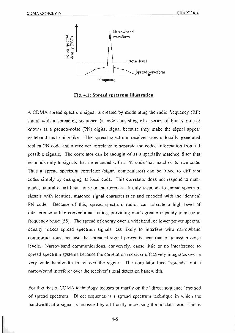
COMA CONCEPTS
Narrowband waveform
Noise level
Spread waveform
Frequency
Fig. 4.1: Spread spectrum illustration
CHAPTER 4
A CDMA spread spectrum signal is created by modulating the radio frequency (RF)
signal with a spreading sequence (a code consisting of a series of binary pulses)
known as a pseudo-noise (PN) digital signal because they make the signal appear
wide band and noise-like. The spread spectrum receiver uses a locally generated
replica PN code and a receiver correlator to separate the coded infonnation from all
possible signals. The correlator can be thought of as a specially matched filter that
responds only to signals that are encoded with a PN code that matches its own code.
Thus a spread spectrum correlator (signal demodulator) can be tuned to different
codes simply by changing its local code. This correlator does not respond to man
made, natural or artificial noise or interference. It only responds to spread spectrum
signals with identical matched signal characteristics and encoded with the identical
PN code. Because of this, spread spectrum radios can tolerate a high level of
interference unlike conventional radios, providing much greater capacity increase in
frequency reuse [58]. The spread of energy over a wideband, or lower power spectral
density makes spread spectrum signals less likely to interfere with narrowband
communications, because the spreaded signal power is near that of gaussian noise
levels. Narrowband communications, conversely, cause little or no interference to
spread spectrum systems because the correlation receiver effectively integrates over a
very wide bandwidth to recover the signal. The correlator then "spreads" out a
narrowband interferer over the receiver 's total detection bandwidth.
For this thesis, COMA technology focuses primarily on the "direct sequence" method
of spread spectrum. Direct sequence is a spread spectrum technique in which the
bandwidth of a signal is increased by artificially increasing the bit data rate. This is
4-5

CDMA CONCEPTS CHAPTER 4
done by breaking each bit into a number of sub-bits called "chips". Assuming this
number is 42, each bit of the original signal would be divided up into 42 separate bits,
or "chips". This results in an increase in the data rate by 42. The increased data rate
is often called the chip rate. By increasing the data rate by 42, the bandwidth is also
increased by 42. The ratio of chip rate to data rate is termed the "processing gain"
and represents the gain in bandwidth. The data signal is divided into chips by
multiplying it by the PN code. The PN code is a sequence of chips ranging form - I to
I (polar or NRZ) or 0 to I (non-polar). The chipped or spread sequence in ADS [7]
can be obtained by two methods depending on the format of the data signal and PN
code. In the case of both the data and PN code signals being in polar or NRZ format,
the spread sequence is obtained by simple multip lication. However, when both the
data and PN code signals are in non-polar or binary format, the spread sequence is
obtained by an Exclusive-NOR (XNOR) operation of both signals.
The basic operation of the transmitter and receiver for direct sequence spread
spectrum will now be described briefly (figure (4.2)).
Transmitter Channel
S,(t)C,(t)C,(t) + S,(I) C,(t)C, (t)
BPF M,(t)
C,(t)
t.o<'l-----.j BPF H Demod ~M,(t) S,(t)c,(I)C,(t) + S,(t) C,(t)C,(t)
Receiver
Fig. 4.2: Direct sequence transmitter and receiver
Assume there are two transmitters (refer to figure (4.2» with two different messages
to be transmitted. Each transmitter can be thought of as being two separate
mobiles/subscribers. The messages M,(t) and M,(t) first go through a modulator to
modulate the message at a higher frequency. For spread spectrum all messages are
modulated on the same carrier frequency. The output of each of the modulators is
SI(t) and S2(t). After the modulator, each signal is multiplied by its own unique PN
code, CI(t) and C2(t). For this example assume that the PN codes are in NRZ or
4-6
COMA CONCEPTS CHAPTER 4
bipolar format (-I to I). After spreading the bandwidth, each signal is transmitted.
Because many signals can be transmitted from different transmitters at the same time,
these transmissions are represented by simply summing their spectrums. At the
receiver end, the incoming signal is the spread spectrum signaL [n order for the
receiver to extract a single message, it must multiply the incoming signal by the
correct PN code. Because the PN code was chosen to range from - I to I, this
technique of multiplying by the PN code works perfectly. Since the original signal at
the transmitter end was multiplied by the PN code, and again multiplied by the same
PN code at the receiver end, the PN code for that particular message is effectively
cancelled out. By eliminating the PN code, the spread spectrum effects for that
particular message is eliminated. The receiver circuit that does this is called a
correlator, and it collapses the spread signal back down to just the original narrow
bandwidth centred at the modulated carrier frequency. The resulting signal is then
passed through a bandpass filter (BPF) centred at the carrier frequency. This
operation selects only the desired signal while rejecting all surrounding frequencies
due to other messages in the spread spectrum. Lastly, the desired signal is
demodulated to eliminate the carrier frequency.
4.5 Filtering
One of the primary requirements of any communication system IS the channel
bandwidth. The design objective is to use this resource as efficiently as possible.
Channel bandwidth can be reduced by utilizing an efficient modulation technique
and/or premodulation (baseband) filtering.
The modulation technique used has an effect on the channel bandwidth. Due tu
restricted spectrum allocation, only bandwidth-efficient modulation techniques can be
chosen. Also, with ever increasing demand for service, the problem of restricted
bandwidth allocation can cause significant degradation of the system. There is thus a
need to provide subscribers with a quality of service which is demand independent.
The property of the basehand data has a significant effect on the channel bandwidth.
To constrain the bandwidth of a modulated carrier, one must examine the baseband
signaL The baseband wavefoml is usually a NRZ (non-retum-to-zero) binary
4-7

CDMA CONCEPTS CHAPTER 4
wavefonn (here logic 1 is represented by an arbitrary voltage Vb held for the bit
duration and logic 0 by the voltage - Vb held for an equal lime). The power spectral
density (PSD) of a baseband waveform is determined by the wavefonn assoc iated
with an individual bit (or symbol). The wavefoml for an individual bit (or symbol) is
a waveform of finite extension of time; its duration being the bit or symbol lime. Any
such waveform oflirnited time duration has a spectrum which extends throughout the
frequency range (f - - 00 to f = +00). The PSD of the NRZ data is shown in figure
(4.3).
Fig. 4.3: Power spectral density ofNRZ data (from 146))
Since the spectrum of the data extends over all frequencies. there is a corresponding
increase in the spectrum of the modulated carrier, hence the importance of filtering.
This is shown in figure (4.4) for BPSK modulation.
-f. - 1I. - f . -f. -I.
~/ , Od.
I.
Fig. 4.4: Power spectral density of BPSK (from 1461l
In cellular communications where different carrier frequencies or many channels are
employed, there would inevitably be overlap in the spectra of the various signals and
correspondingly a receiver tuned to one carrier would also receive, albeit at a lower
level , a signal in a different channel. This overlapping of spectra causes interchannel
4-8

CDMA CONCEPTS CHAPTER 4
interference. For example, in the case of BPSK (also QPSK and OQPSK), the 1st
sidelobe is relatively large when compared to the main lobe (sidelobe is only 14dB
down the mainlobe). Since efficient spectrum utilization is extremely important in
order to maximize the number of simultaneous users in a multi-user communication
system, standardization agencies such as the FCC (Federal Communications
Commission) require that the sidelobes produced in different modulation schemes be
reduced below certain specified limits. This interchannel interference problem is so
serious that standardization agencies will not pennit these systems to be used except
with bandpass filtering at the carrier frequency (i.e. at the transmitter output) to
suppress the side lobes.
In addition to bandpass filtering at the carrier frequency, filtering is also perfonned on
the data waveform. Any fast transition in a signal, whether it be amplitude, phase or
fTequency wi ll require a wide occupied bandwidth. Filtering helps to slow down and
smoothen these transitions (in I and Q) thereby narrowing the occupied bandwidth.
Filtering reduces interference because it reduces the tendency of one signal or one
transmitter to interfere with another (especially in a FDMA system). At the receiver,
reduced bandwidth improves sensitivity because more noise and interference are
rejected. The spectrum can be minimized by passing the baseband wavefonn through
a lowpass filter to remove the offending spectral range and sidelobes. However, it
should be noted that this premodulation fi ltering distorts the signal and as a result,
there is a partial overlap of a bit (symbol) and its adjacent bits in a single channel.
This overlap is called intersymbol interference (lSI). ISI can be somewhat alleviated
by the use of equalizers (filter-type structures) at the receiver. Equalizers are
implemented in baseband. Basically, they undo the adverse effects introduced by the
premodulation filter, So any unfiltered baseband waveform must cause interchannel
interference and if it is filtered, interchannel interference can be reduced but only at
the expense of causing intersymbol interference. Thus a tradeoff has to be made.
Other tradeoffs are that filtering makes the radio more complex and can make them
larger, especially if implemented in an analog fashion.
In order to detennine the bandwidth efficiency of the different modulation techniques
used in cellular communications, it is necessary to consider the different definitions of
bandwidth. The two most commonly used bandwidth definitions are:
4-9
COMA CONCEPTS CHAPTER 4
(a) Null-te-null bandwidth - is the width of the main spectral lobe where most of the
signal power is contained.
(b) 99% of power - adopted by the FCC and states that the occupied bandwidth is the
band which leaves exactly 0.5% of the signal power above the upper band limit.
and exactly 0.5% of the signal power below the lower band limit. Thus, 99% of
the signal power is contained inside the occupied band.
Using the 99% of power bandwidth criterion for a channel data rate (fb) of 4.096MHz
(data rate after spreading) for the proposed third generation WCDMA [I] , BPSK
modulation would require nearly Sfb or 32.768MHz, which makes it unsuitable. This
poor bandwidth efficiency can be improved using QPSK (or OQPSK) where twice the
infonn ation can be carried in the same amount of channel bandwidth (compared to
BPSK). Using the 99% of power bandwidth criterion, the total channel bandwidth
equals 4fb or 16.384MHz for a data rate (after spreading) of 4.096MHz. Thus, QPSK
modulation provides a substantial savings (factor of 2) in channel bandwidth over
BPSK.
The null -to-null bandwidth criterion is also often used. In BPSK, QPSK and OQPSK
this translates to the mainlobe power. In these cases 90% of the power is contained in
the mainlobe. To accommodate this main lobe power, the premodulation filters and
band pass filters would have to have passbands of 2fb in the case of BPSK and rb in the
case of QPSK and OQPSK. Again, using the proposed WCDMA with a data rate
4.096MHz (after spreading), BPSK would require an RF bandwidth of 8.192MHz
whi le QPSK and OQPSK would require 4.096MHz. In the IS-95 CDMA system
employing QPSK (at mobile) and OQPSK (at base) modulation the rate of the final
spread signal is 1.2288MHz resulting in an RF bandwidth of approximately 1.2SrvrHz.
The 3dB bandwidth is 1.23MHz. The baseband signal after spreading is bandlimited
by a digital filter that provides a sharp frequency roll-off and results in a nearly square
spectral shape that is 1.23MHz wide at the 3dB point. In the case of third generation
proposals, a nominal bandwidth of 5MHz has been proposed. This bandwidth is
commensurate with the minimum chip rate of 4.096MHz specified by \VCDMA [I].
Other proposed chipping rates are 8. 192MHz and 16.384MHz resulting in an RF
bandwidth of 10MHz and 20MHZ respectively [ I]. [t should be noted that all these
bandwidths were proposed using QPSK/OQPSK modulation.
4-10

COMA CONCEPTS CHAPTER 4
The most common varieties of base band filtering are
• Raised cosine (Nyquist)
• Square-root raised cosine (transmitter receiver matched filter)
• Gaussian filtering
4.5.1 Nvguist or raised cosine filter
The raised cosine filter is a class of Nyquist filters. Nyquist filters have the property
that their impulse response rings at the symbol rate. The filter is chosen to ring or
have the impulse response cross through zero at the symbol clock frequency. The
time response of the filter goes through zero with a period that exactly corresponds to
the symbol spacing. Adjacent symbols do not interfere with each other at the symbol
times because the response equals zero at all symbol times except the centre (desired)
one. Nyquist filters filter the signal without blurring the symbols together at the
symbols times. This is important for transmitting infonnation without errors caused
by intersymbol interference. Note that intersymbol interference does ex ist at all times
except at the symbol (decision) times.
4.5.2 Square root raised cosine filter (transmitter-receiver matched filters)
In the square root raised cosine filter, the raised cosine filter described above is split,
halfbeing in the transmit path and half in the receiver path. In this case root Nyquist
filters (commonly called root raised cosine) are used in each path, so that the
combined response is that ofa Nyquist filter.
Filtering is desired at both the transmitter and receiver. Filtering in the transmitter
reduces the adjacent power radiation of the transmitter, and thus its potential for
interfering with other transmitters. Filtering at the receiver reduces the effect of
broadband noise and also interference from other transmitters in nearby channels. To
get zero intersymbol interference, both filters are designed until the combined result
of the filters and the rest of the system is a full Nyquist filter. Potential differences
can cause problems in manufacturing because the transmitter and receiver are often
manufactured by different companies. The receiver may be a small hand-held
portable and the transmitter may be a large base station. If the design is perfomled
correctly the results are the best data rate, the most efficient radio, and reduced effects
4-11

CDMA CONCEPTS CHAPTER 4
of interference and noise. This is the reason for root Nyquist filters being used in
transmitters and receivers as ~ Nyquist x ~ Nyqllist = Nyquist .
4.5.2.1 Filter bandwidth parameter (a )
The sharpness of a raised cosine filter is described by the filter bandwidth parameter
(a). a gives a direct measure of the occupied bandwidth of the system and is
calculated as
occupied bandwidth = symbol rate x (I + a)
Figure (4.5) shows raised cosine filter responses for different a.
o. -........: , , ·
" , · 6 , ,
"-, ,\ · a - to
6 " aeO.S -'\v. ' a-0.3 • i .~ '* . K,(' a-O -i \ \ : .'
o.
o.
V , ""-, t--.... o o 0.2 0.' 0.' 0.6
Fs : Symbol Ra!.e
Fig. 4.5: Raised cosine filter responses as a function of (a )
(4.2)
If the filter had a perfect (brick wall) characteristic with sharp transitions, a is zero
and the occupied bandwidth (using equation (4.2)) would be the symbol rate .
However, this as an ideal case hut this is not practical. a = 0 is impossible to
implement. a is also known as the excess bandwidth factor since it indicates the
amount of occupied bandwidth that wi ll be required in excess of the ideal occupied
bandwidth (which would be the same as the symbol rate). At the other extreme, a
broader filter with a = I is easier to implement and has an occupied bandwidth of
twice the symbol rate. Thus an a = I uses twice as much bandwidth than that of
a = O. In practice, it is possible to implement a < 0.2 and make good, compact,
practical radios. The lower the a, the smaller the occupied bandwidth and the
smoother the transitions between I and Q states. Typical values range from 0.35 to
0.5 though some video systems use an a as low as 0.1 1.
4-12
COMA CONCEPTS CHAPTER 4
4.5.3 Gaussian filter
Gaussian filters are used In GSM. GSM uses GMSK (Gaussian Minimum Shift
Keying) modulation. There is a small blurring of symbols on each of the four states in
a GSM signal because the Gauss ian filter does not have zero intersymbol interference.
The phase stales vary somewhat thereby causing blurring of the symbols. Thus the
wireless system designer must decide on the amount of intersymbol interference that
can be tolerated and combine that with noise and interference. However, Gaussian
fi lters are used in GSM because of their advantages in carrier power, occupied
bandwidth and symbol clock recovery. It is Gaussian in shape in both the time and
frequency domains and it does not ring as in the case of raised cosine filters. Its effect
in the time domain are relatively short and each symbol interacts significantly with
only the preceding and succeeding symbols thereby causing intersymbol interference.
This reduces the tendency for particular sequences of symbols to interact which
makes amplifiers efficient and easier to build.
The corresponding term for the filter bandwidth parameter in a Gaussian filter is the
bandwidth time product (Bb T). Occupied bandwidth cannot be stated in terms of Bb T
because a Gaussian filter's frequency response does not go identically to zero, as does
a raised cosine. Common values ofBbT are 0.3 to 0.5. More detai ls of the Gaussian
filter and BbT are provided in the next section.
4.5.3.1 Gaussian filtering as used in MSK modulation
Filtering, in certain situations using QPSK or OQPSK does not resolve the problem of
interchannel interference. These modulation techniques produce signals of constant
amplitude, the information content being borne by phase changes. These phase
changes are abrupt (90' in the case ofOQPSK and 180' in the case ofQPSK). Now it
turns out that when such waveforms with abrupt phase changes, are fi ltered to
suppress sidebands, the effect of the filter, at the times of the abrupt phase changes, is
to cause substantial changes in the amplitude of the waveform. Such amplitude
variations can cause problems in QPSK communication systems which employ
repeaters (Le. stations which receive and rebroadcast signals). These stations employ
non linear power ampli fier stages in their transmitters. Because of their non linearity,
they generate spectral components outside the range of the mainlobe thereby undoing
the effect of bandlimiting filtering and causing interchannel interference. In this
4-13
CDMA CONCEPTS CHAPTER 4
matter QPSK is a substantially worse offender than OQPSK because of its larger
phase change.
The above-mentioned problem can be resolved using another modulation technique,
called minimum shift keying (MSK) which is a form of OQPSK in which the symbol
pulse shape is a half-cycle sinusoid, rather than the usual rectangular fonn. MSK has
the following distinctive properties:
(a) The baseband waveform that multiplies the quadrature carrier is much "smoother"
than the abrupt rectangular waveform of QPSK. The spectrum of MSK has a
main centre lobe which is 1.5 times as wide as that of QPSK. However, the
sidelobes with respect to the main lobe is smaller than that of QPSK (the first
sidelobe of BPSK, QPSK and OQPSK is only 14dB down the mainlobe!). Thus
filtering is much easier in MSK.
(b) The MSK waveform exhibits phase continuity I. e. there are no abrupt phase
changes as in QPSK. As a result interchannel interference caused by nonlinear
amplifiers is avoided.
The spectral efficiency of MSK is considerably greater than that of QPSKlOQPSK.
Using the 99% of signal power bandwidth criterion, MSK would require a bandwidth
of 1.2fb compared to 4fb for QPSKlOQPSK. For a 4.096MHz data rate, this translates
to an RF bandwidth of 4.9 152MHz for MSK and 16.384MHz for QPSKlOQPSK.
The null-to-null bandwidth criterion yields 6.144MHz (1.5 x 4.096MHz) for MSK
and 4.096MHz for QPSKlOQPSK (main lobe for MSK is 1.5 times as large as that for
QPSK and OQPSK).
As mentioned previously. GSM makes use of MSK modulation. A baseband
Gaussian filter is used as the premodulation filter to obtain a linear phase
characteristic. This filtered version of MSK is known as GMSK. Both the sidelobe
power level and the width of the mainlobe is reduced by this Gaussian filter. In spite
of its increased spectral efficiency over QPSKJOQPSK, MSK modulation has not
been proposed for third generation COMA systems. Instead linear modulation
techniques (BPSK, QPSK and OQPSK) have been proposed for wideband third
generation CDMA because of their good modulation efficiency [I]. Another reason
can be speculated to be that the VLSI implementation of a GMSK modulator is
4-14

COMA CONCEPTS CHAPTER 4
difficult to realize. The use of constant·envelope modulation schemes such as MSK
are limited to a spectral efficiency of approximately 1 bitlseclHz, regardless of the
number of modulation levels used. However, linear modulation schemes such as
shaped PSK, which uses linear power amplifiers, can achieve efficiencies greater than
1 hitlseclHz. Greater efficiencies can be attained with a higher number of modulation
levels used at the expense of a higher bit error rate (BER) due to the reduced distance
between constellation points. Because of the use of linear amplifiers, linear
modulation techniques can provide better oUl-of-band radiation perfonnance.
increasing the spectral efficiency of the system further. Advances in technology and
devices have made the use of linear amplifiers feasible and cost-effective.
Bandlimited linear modulation methods utilizing nonlinear power amplifiers result in
spectrum leakage to adjacent carriers [59]. Therefore, especially in the uplink (mobile
to base), the modulated signal should be able to tolerate nonlinear power amplifier
effects. Once the modulation method has been fixed, pulse shaping at baseband
determines the final spectrum properties. The roll-off factor depends on the power
ampl ifier (PA) linearity and adjacent channel attenuation. Spectrum leakage to
adjacent channels can be controlled by backing off the PA or by using some
Iinearization method to equalize the nonlinearities of the power amplifier. However,
both methods decrease the achievable PA efficiency when compared to modulation
schemes that have constant envelope and can be amplified with power efficient
nonlinear power amplifiers [59].
The CTIA standardization agency has recommended that the adjacent-channel
interference should be below - 60dB for cellular radio [60}. One of the parameters of
interest in the design of the Gaussian baseband filter is the bandwidth time product
(normalized 3dB bandwidth), Bb T where T is the data pulse width. The power
spectrum density plot as a function of normalized frequency difference from the
carrier centre frequency Cf - fc)T, with the normalized 3dB bandwidth of the baseband
Gaussian filter (Bb T) as a parameter is shown in figure (4.6).
4-15
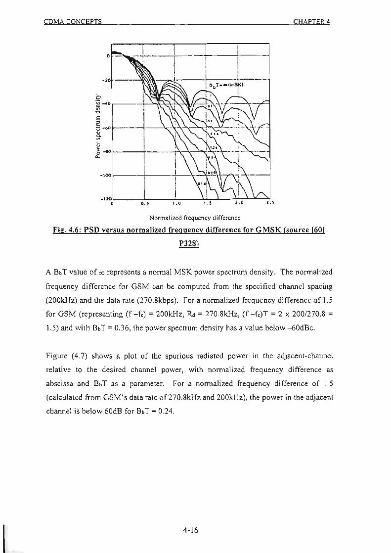
CDMA CONCEPTS CHA PTER 4
Nonnalized frequency difference
Fig. 4.6: PSD versus normalized frequency difference for GMSK (source 1601
P328)
A BbT value of co represents a normal MSK power spectrum density. The normal ized
frequency difference for GSM can be computed from the specified channel spacing
(200kHz) and the data rate (270.8kbps). For a nonnalized frequency difference of 1.5
for GSM (representing (r - f,) ~ 200kHz, Rd ~ 270.8kHz, (f - f,)T ~ 2 x 200/270.8 ~
1.5) and with Bb T ~ 0.36, the power spectrum density has a value below -60dBc.
Figure (4.7) shows a plot of the spurious radiated power in the adjacent-channel
relative to the desired channel power, with normal ized frequency difference as
abscissa and BbT as a parameter. For a normalized frequency difference of 1.5
(calculated from GSM's data rate of270.8kHz and 200kHz), the power in the adjacent
channel is below 60dB for Bb T ~ 0.24.
4-16

CDMA CONCEPTS CHAPTER 4
0
in -20 >'-~
~ -'0 E 8 • -60 '<f • • " ." -80
~ It •
.~ -100
;; «
-120
0
NOI'malized frequency separation
Fig. 4.7: Relative power radiated in adjacent channel (source 1601 P329)
Thus, the baseband Gaussian filter of GMSK can have a maximum nonnalized 3dB
bandwidth or bandwidth time product (Bb T) of 0.24 in order to satisfy the adjacent
channel requirement of - 60dB.
ill addition to the European GSM system, GMSK has also been adopted by DECT
(Digital European Cordless Telephone). For GSM, the normalized bandwidth ofBbT
is 0.3 with a total channel data rate of 270.8kbps has been adopted. Thus the
bandwidth of the lowpass filter is 81kHz (0.3 x 270.Skbps).
From figure (4.7), it can be seen that the CTrA recommended value of -60dB
adjacent-channel interference cannot be met in the GSM system employing BbT:::: 0.3.
The choice of Bb T of 0.3 for GSM is influenced by BER performance at the expense
of not meeting the CTIA's recommended value of -60dB for adjacent-channel
interference. A BbT value of less than 0.3 increases the BER exponentially due to a
drastic reduction in signal power. DECT has adopted BbT = 0.5 with a data rate of
1.1 52Mbps. This corresponds to a filter bandwidth of 576kHz (0.5 x 1.1 52Mbps).
DECT also does not rneet the CTIA's -60dB recornmended adjacent-channel
interference. An adjacent-channel interference of nearly -40dB can only be rnet.
Since the DEeT system reassigns channels as the interference goes up, -40dB
adjacent-channel interference may be tolerable. Figure (4.8) shows a plot of BER
4-17
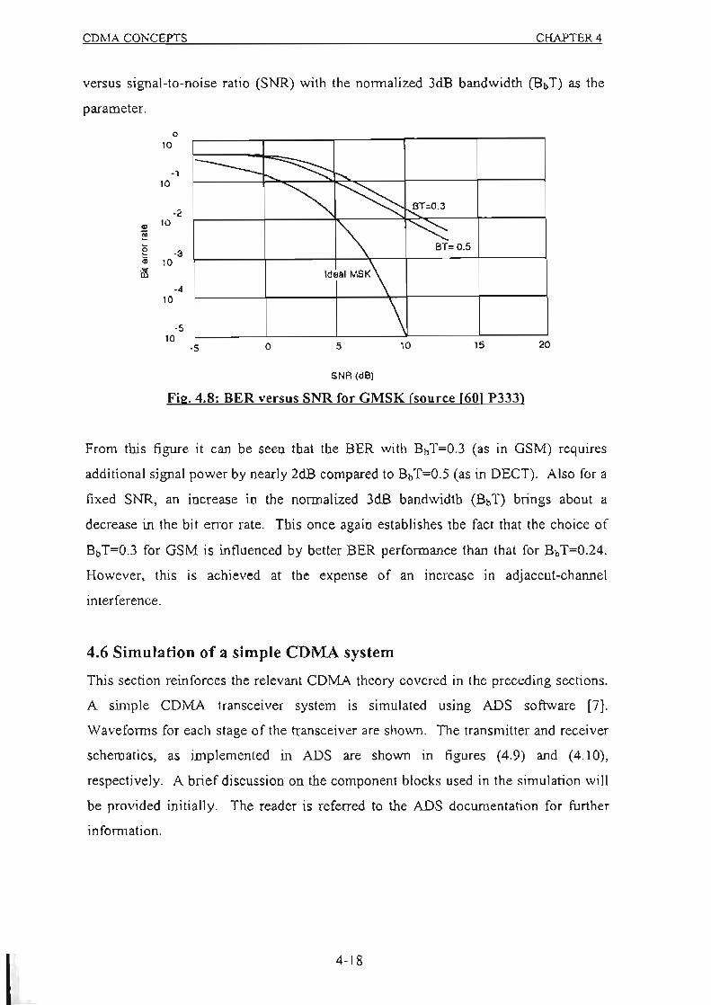
CDMA CONCE PTS CHAPTER 4
versus signal-to-noise ratio (SNR) with the normalized 3dB bandwidth (Bb T) as the
parameter.
0
'0
-, -.....; '0
-2 ~ ~ 8TzO.3
• ' 0 ;;
" -3 i '0 -~
'" -. ' 0
-s
1,\ ~.o_s IdoalMSK\
\ '0
-s o s '0 " 20
SNR (dB)
Fig. 4.8: BER versus SNR for GMSK (source [60) P333)
From this figure it can be seen that the BER with BbT=O.3 (as in GSM) requires
additional signal power by nearly 2dB compared to BbT~0.5 <as in DECT). Also for a
fixed SNR. an increase in the normalized 3dB bandwidth (Bb T) brings about a
decrease in the bit error rate. This once again establishes the fact that the choice of
Bb T~0.3 for GSM is influenced by better BER performance than that for Bb T~0.24_
However, this is achieved at the expense of an increase in adjacent-channel
interference.
4.6 Simulation of a simple COMA system
This section reinforces the relevant CDMA theory covered in the preceding sections.
A simple CDMA transceiver system is simulated using ADS software [7].
Wavefomls for each stage of the transceiver are shown. The transmitter and receiver
schematics, as implemented in ADS are shown in figures (4.9) and (4 .10),
respectively. A brief discussion on the component blocks used in the simulation will
be provided initially. The reader is referred to the ADS documentation for further
information.
4-18
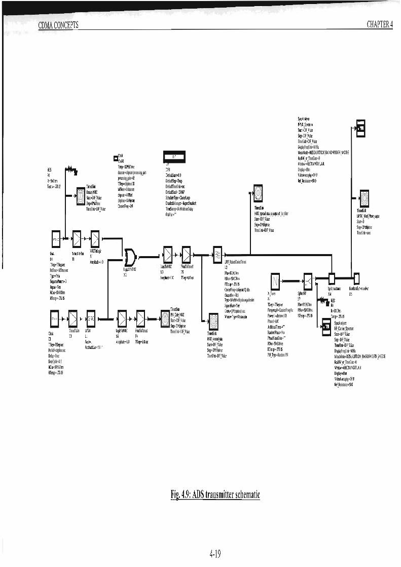
CDMA CONCEPTS
RES RI R=~OIrn Tonp=·27l. ~
.,.VAR -VARI
TSQl=INine dltlra~=dJp"ab'~o::e;sJuin ~o::e;suwm=42 TS!,(=dijJindll lItfine=V!lllara~
dJp"a~=W1f6 dijJine=VdJp"at CarruFr«j=leJ
OFI DefailiStJrt=QO DefailiSQl=Ts\Jl DefatliTineUli=soc DefaIJrJetl!=12JI))7 S~=CUul.ujJ DemkM.=RqxrtDemI: imeStIn1p=N!Mtiira~elay
Mar =""
~ ~~D~'-"'" ~"' __ -JI TS!,(=TSlllSOC ~TiNRZ FbltToTined
LPFRa5IllliD"eTined 1.2 -
BifI"me=lJ(finesoc ~XNOR2 Xl F8 T)~.Prlli X2 Am~iul!= 1.0 TSlll=QOsoc S~3Irl:n=l Rqrat=Ye; RO~=il.OOIrn RTonp=·m~
~~B M Cl TSI.'p=TStqJ soc Perlxl=~nesoc Deby=Ose: D~=Ql RO~=il.OOIrn RTonp=·m~
fnnOOfdrt LFSR TJ LI
Setl!=1 Filrlli:Itit="J I"
r L ~ L- ~~ai~v~ 1j~~Sty=21\ilj1Dne Lq,tTiNRZ FiElToTinro imeUIi=DF Vahl: ~ R -AIII~= 1.0 TS!'(=QO soc
fnnellliIt NRZ)~laLd!~ Stlrt=DF Vahl:
R1n=jlOOhn RO~=il.OOlm RTIl11p=·27l.ll CarerFr«j=(dJp"ab'~Hz mssBw=Ql T~=MllI:Iwmjlile~ S!IllfeRa!=Ye; De~y=(41d~ne)soc Wum.vT)!t=Ra:tlrgjar
SqJ=21~ne TuneUrit=DFJahl:
TUnellliIt NRZ}~e:kLd!~}LOJilI_d)Lml.l" StJrt=DFVaIu! Sty=21~ne TineUIi=DF_Vahl:
N T(Jl!! Ni TSep=TSl.'psoc Frll!-&Yl=Carrfl"Fr«j Hz P(),\'er l =dm\)N(I~
Pln\el=UO AdIiXntIT(Jl!!='" RaJlbnPlIISe=No PllISeNdseDa~="
RO~=il.OOhn
RTanp=·mll PNJ~=RaJlbnPN
Fig. 4.9: ADS transmitter schematic
4-19
SJItArni)1er BPSK Sjlrtrun Stlrl=DF Vahl: SqFDFjahl: ianeUIi=DP Vahl: D~pafr«jU~=MHz
CHAPTER 4
MeasMIlI:=RESO LUTION BANDWIDTH MODE ResBW a TmleGa~=O - -WirIb.v""=REcrANGULAR Dl\[i1y=tIlm V®\\eI~=OFF R(Res51m=il.O
SjllI.'rRF S7 R1n=~. OOhn
RO~=il.OOhn RTanp=·m ll
RES R4 R=~OIrn
Tanp=·27l. ~
SJItArni)1er RF_Carr~JjlrtrU11 Stlrt=DF Vahl: S~DFjahl: TineUtl=DF Vahl: D~iJafr«jUtii=MHz
TinelllUt BPSK _Mal}IaIe_($t StJrt=O Sty=21\ilj1Dne iDneUtl=tre;
MeasMIlI:=RESOLUTlON BAN DWIDTH MODE ResBWail1leGat=O - -WirIb.v-=RECrANGULAR D~iJay=d)1I1
Viro!. \elats=OFF R(Res51m=il.O

CDMA CONCEPTS
~ NJ(TCS N6 TSIep=TSlepso: Pr~l=mlMH!
PCM'erl =, OIOW Pillscl=O,O AdimITars= RBrd:mPlllle=No PlllleNciseDaI!= RO\X=j),OOIm RTemp=·m,ll PN})p:=RBrd:mPN
NIJI1 =1 MilerRF MI Rin=i),OOIm ROUl=i),OOIm RTemp=·m. ll T)p:=LOmmRF RfRcj •• :m ImRq=·:m U&j=.:m NciseP~c=O LCcmp='OOO'
NJ(TCS N2 TSIep=TSlepso: Pr~yl ='~}MH!
PCM'erl=, OIOW Plmel=O,O AdimfI'ars= RBrd:mPlllle=No PlllleNdscDaIII=" RO~=i), OOIm
RT~np=·m,ll
PN.T)p:=R!IlImPN
MilerRF M2 Rin=i),OOIm ROUl=i),OOIm RTemp=·m.ll T)p:=LOmmRF RfRej=·:m ImRq=·:m U&j=.:m NdseF~c=O LCanp='OOO'
LPF-'las~~Tmed 12 Rin=i),OOIm ROut. i),OOIm RTemp=·m.ll CartrPr~=(cliir~~ H! ElJ.'eSsBw =Ql T)p:=1 miMe mal!l SiplreRa:t=Ycs DeIly=(4~li!1ine) so:
WIxlJ,vT)p:=R.
TIn&Sir« ReceTier..NRZ.SlleOO.dYa.&.iJU.d)!ilJiler SIilrI=DP_Vahl SkJl=21'tli!1ine
Spo:Allllyzer TlneUnI=DP.Valt IP.spo:~1JI1 Sblrl =DF.V~
SkJl=DF.Vare T~lcUnI=DP Ve D~Jli)Fr~Urii=MH! MealMaI!=RESOLUTION .BANDWIDTH .MODE RcsBWaTineO~=O WIxIJ,v-=REcrANGULAR D~Jliy=dBm
VKlxAlero~=OFP Rer.Rcs~wrre=i), O
Oxk
~~Iep=TSIep SO: fj~~, ~RG .. Perm=.eso: bJ ,. lj De1ay=Oso: TlnedTdtt LPS ~ToNRZ Dil)C)I:~ =Ql Ti LI XI ROut=i),OOIm S=I=I Am~ilil= 1.0 RTemp=·m. ll Pem:kLtil='ll'
TlnedTdlbJ! M~ PbnToTined PI T2 M4 TSIep=O,Oso:
Tin&S1t
SIiI'l=DFV~ SI.'p=21'tllpme
Deb)RF 01 Rin=i),OOIm ROut=j),OOml RTemp=·m,ll Deby=(8'c1iplllc) so:
.~ .. C} ~Im~tr I ~ToTlned
L1 Il TSIep=O,Oso:
Oxk TinedTdil
~1ep=TSICp SO: Tl Perm=IitTineso: Deby=(8'cli!1inc) so: Dil)C)C~=QI ROut=i),OOI:~ _______ ....
CHAPTER 4
-I "'l • . ~.m."'."-,-"",.'-""'-'~
T~leUn'=DF_V~ H---RES"""-i RES RI R=i)O~n
Tanp=·m. ll
Fig. 4.1 0: ADS receiver schematic
4·20
1~lJI1pTmed SamJlAIIIlIiI 12 SI
Rin=i)OOIm R1n=i),OOIm ROUl=lQOOIm ROUl=lQOOIm RTemp=.m.ll RTemp··m.ll
Dr~=O
I TinedSDt rn Multjftr.~
SWI'I=DP Ve Stp=2ll1iTlnc TaneU nI= DP.Ve
Rl R=i)OIm Temp=·m,ll
TIn&Sir« ReceTierduaOll SlBn=DPf~ SI.'p=21"Tinc TlneUnI=DP.Y ahl

CDMA CONCEPTS CHAPTER 4
ADS block label elossary
VAR: This block allows variables to be declared. Values are also assigned to these
variables. Variables such as the simulation stop time (Tstop) , data rate, processing
gain, simulation sampling time (TStep) are declared in this block. The simulation
sampling time (TStep) is of importance. Its value is chosen such that
TStep<llMaxirnum baseband data rate. In this case, the maximum basehand data rate
corresponds to the chip rate (4.096:Mllz). A value of one-twentieth of the chip timt:
interval was used for Tstep. It should also be noted that a decrease in the sampling
time results in an increase in the simulation run time.
DF cOlltroller: The Data Flow (DF) controller is used to control the simulation start
and stop times. The DefaultStop field in this instance is specified to be the variable
Tstop (declared in the V AR block). The DefaultStart time is usually zero. The time
unit can be specified in the DefaultTimeUnit field.
TimedSillk: This enables display of waveforms as a function of time. The Start and
Stop fields aJlow the waveform to be displayed over a specified time frame.
Data: This block generates data in NRZ format. A BitTime field exists for the input
of the datalbit time. The length of the data can be specified in the SequencePattem
field. The data is displayed in the time sink called Datain_NRZ.
NRZToLogic: Converts NRZ timed data to a binary datastream format.
LogicToNRZ: Converts a binary datastream to a NRZ timed data [annat.
TimedTolllt~ FloatToTimed, TimeToFloat, /lItToTime(/: These blocks enable
conversion from one data format to another.
LogicXNOR2, Logic/llverter: These are logic gates that perform the XNOR and
inverter operations, respectively. The spreading process is performed using the 2
input XNOR gate (LogicXNOR2).
LFSR: This is a linear feedback shift register that was used to generate the PN code.
In this case, the fields for the initial value (Seed) and the Feedback were set to I and
"3 I", respectively. The Feedback field of "3 I" implies the use of a 3 stage shi ft
register. Thus the PN code has a length of 7 (2 ' -1).
Clock: This block (Cl) was used to drive the shift registers (LFSR). Its period was
set to the chip time. Thus the PN code generated by the LFSR is at the chip rate.
LPF_Raise([CosilleTimed: This is a raised cosine low pass filter. Two of these
filters (matched) were used in the transceiver. Some of the fie lds for this block were
discussed in section (4.5.2).
4-21

CDMA CONCEPTS CHAPTER 4
N tones: These blocks were used to generate the various carrier frequencies in the
system. Fields exist for both frequency and power level.
SpecAIJalyzer : This is a spectrum analyzer sink used to display the spectrum of
signals. For example, the spectrum analyzer named BPSK_Spectrum is used to
display the 2GHz BPSK spectrum at the transmitter. Fields are similar to those of a
spectrum analyzer.
SplitterRF: This is a simulation device that splits or provides an alternalt: path for the
signal. However, it is not a power splitter. The signal at the output legs of the device
are a repl ica of that at the input.
hpsk_ Inodlllator, BasehulldEsNoreceiver: These arc subnetworks. For example, the
subnetwork named BasebanEsNoreceiver was created by fanning a network of all the
receiver components. By clicking on this network, the receiver components (in figure
(4.10» can be viewed. Subnetworks simplify the schematic.
MixerRF: As the name suggests this is simply a mixer. In the receiver schematic
(figure (4.10», mixers M I and M2 are used as a downconverter and demodulator,
respectively.
Mpy2: This is a 2 input multiplier. In this context, it is used to perform the
despreading operation (recall an XNOR gate could also be used).
DelayRF: This component is used to introduce a time delay. In the receiver it is used
to synchronize the PN code with the demodulated (spread) data. The receiver PN
code was delayed by 8 chips corresponding to the total delay of the two root raised
cosine filters.
IlItDumpTimed, S ampleA lldH old: These are just integrate and dump and sample and
hold circuits. In the receiver (figure (4.10», they are used (in conjunction with the
despreading process) to retrieve the transmitted data.
The CDMA system will now be discussed: The input message signal is assumed to
consist of an arbitrary chosen 97.5kbps data stream that is spread by a wideband
CDMA signal with a chip rate of 4.096MHz. Thus this corresponds to a system
processing gain of 42. The 4.096MHz chip rate is the minimum rate specified by
WCDMA [1] in Europe and Japan. In the simulation, the message bit stream of bit
time 1 0.254~s (1 /97.5kHz) was set to consist of an eight bit (110100 10) repetit ive
stream. For the purpose of simplicity in demonstrating CDMA concepts, a PN code
4-22
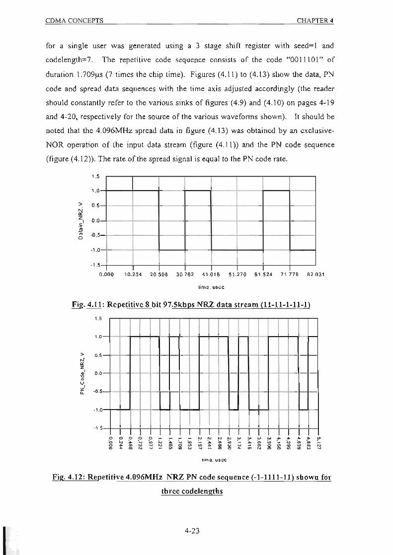
COMA CONCEPTS CHAPTER 4
for a single user was generated using a 3 stage shift register with seed= l and
codelength=7. The repetitive code sequence consists of the code "00 III 01" of
duration 1.709~s (7 times the chip time). Figures (4.11) to (4.13) show the data, P
code and spread data sequences with the time axis adjusted accordingly (the reader
should constantly refer to the various sinks of figures (4.9) and (4.10) on pages 4-1 9
and 4-20, respective ly for the source of the various wavefonns shown). It should be
noted that the 4.096MHz spread data in figure (4.13) was obtained by an exclusive
NOR operation of the input data stream (figure (4.11» and the PN code sequence
(figure (4.12». The rate of the spread signal is equal to the PN code rate.
1.5
1.0 I I I > N
0 .5
~ z 0 .0 .s ' ~ • ·0 .5 C
-1.0
-1.5 I I I I , , , 0.000 10.254 20.508 30 .762 41 .016 51 .270 61.524 71 .778 82.031
lime , usec
Fig. 4. 11 : Repetitive 8 bit 97.5kbps NRZ data stream (I 1-11-1 -1 I-I)
1.5
1.0 I I I > 0.5 N ~ z .' 0 .0 ~ u z' -0.5 ~
-1 .0
· 1.5 I I I I I I I I
0 0 0 0 0 - - - - , N N N ~ W W W ~ • • • ~
" N .. " ~ N .. " ~ '" .. .. ~
~ .. .. ~ - " .. ..
0 • • w ~ ~ • 0 ~ , • w - • 0 ~ ~ w • N 0 • • N ~ ~ ~ w ~ • 0 • • N • 0 ~ ~ w ~
time. usec
Fig. 4. 12 : Repetitive 4.096MHz NRZ PN code sequence (-1-1111-1 1) shown for
three codelengths
4-23

CDMA CONCEPTS CHAPTER 4
U
LO 1- 1 1 1 1 > ,; 0.5
• ~, • 0.0 • -~ • N' -0.5 « z
-1 .0
-1.5 1 I
0 0 0 0 0 ~ ~ ~ ~ N N N N W W W W ~ • • • ~
" " .. ~ '" " .. ~ '" .. '" '" ~ .. '" '" ~ '" <-
0 • • w ~ ~ • g ~ • , • w • 0 ~ • w • N 0 • • N ~ ~ w ~ • 0 • • N • 0 ~ • w ~
tim e. usec
Fig. 4.13: NRZ 4.096MHz spread data sbown for 3 codelengtbs
This NRZ spread data, after square root raised cosine premodulation filtering (figure
(4.14)), is used to BPSK modulate an arbitrary chosen 20Hz, IOdBm (IOmW) RF
carrier. The root raised cosine filter (in both the transmi tter and receiver) each have a
delay of 4 chips or 976.6nS. Figure (4.1 5) shows the ADS implementation of the
BPSK modulator. The BPSK spectrum is shown in figure (4.16).
, .. > ai ~ 1.0
.' ~ 0.5
~: 0.0
.. "", .0 ~
I '", -, 0 N « z
I " I -
IV V
'\ - -
\ \ 'J \
§ ~ i~~~i~~~;i~~~§§;i~!s t ime, usec
Fig. 4.14: NRZ 4.096MHz spread data after root raised cosine filtering at
transmitter
4-24

CDMA CONCEPTS CHAPTER 4
~~~I--· -- ~~ll -~ --~EJI-9 "'J ?hauS",tIRF p~ ......... ' ,. IC~SPI)' PI .,............. ...-""."
E 2
i ~,
~
"
RI~.""'oo~ SZ "'""~O.[/ on", "llv'_~U [/ 0 ..... II'O.';~O I) 0..... "11 .... __ 2'1 '<;' I" • ...., __ 17} IS ...... ~~,.
, •• 1·0 • ,\,~"'--2CO ••• .,·0
•• ' .. '·~_1 __ 100
~!"'.'''old_a ~ '0_1.0 ... 10'''.0 He rQoZ_O .c< TO' ,~oo ne
.. ,".~c 0 n .....
"o,,'=)U ~ 'l ..... Ill... -171. ')
"OH' 'I l!!,v
Fig. 4.15: BPSK modulator
Fig. 4.16: 2GHz RF BPSK spectrum (ADS)
",,,=)0 ..... "O'~' =l U " ...... "l ___ 27J.'
This simulated transmitted signal is then injected into the RF front-end receiver where
downconversion and demodulation are performed. Downconversion to an IF of
70MHZ is performed using a mixer. The IF spectrum is shown in figure (4.17).
4-25
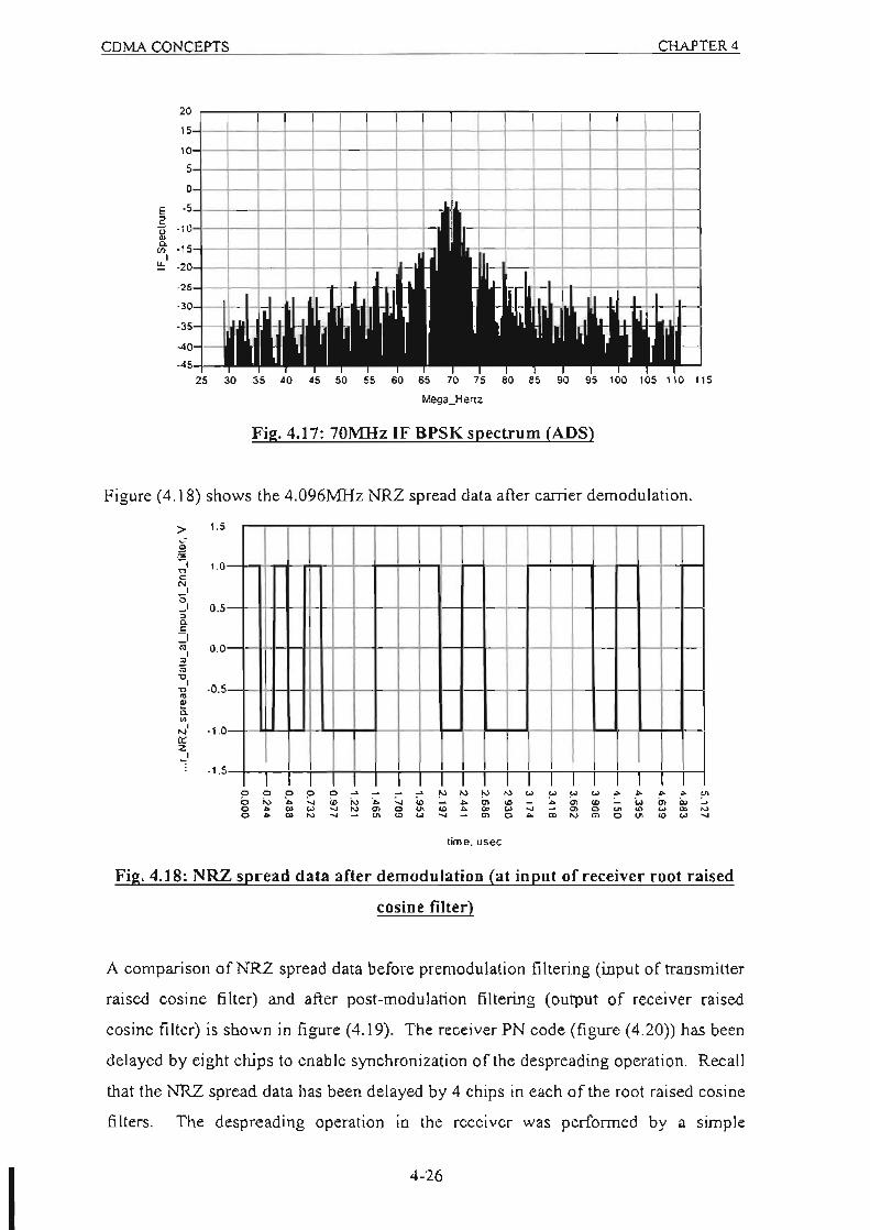
CDMA CONCEPTS CHAPTER 4
~
~ -'54--+--+--+--~4--4--4-~
Fig. 4.17: 70MHz IF BPSK spectrum (ADS)
Figure (4. 18) shows the 4.096MHz NRZ spread data after carrier demodulation.
> L5 .. ~ ~ , LO ~
I I I I I I c ~, ~, 0 .5 , ~
.< -' • 0 .0 , • • ~ ,
-o.s ~ • ~ • N' -1.0 ~ z
" -1 .5 I I I I I I
0 0 0 0 0 ~ ~ ~ N N N N P ~ P ~ • • • • ~
" N • ~ • ~ ;. , ;. ~ • • • ~ • • ~ ~ " " ~ 0 • • ~ ~ ~ • 0 ~ , • ~ ~ ; • 0 ~ • " • N
0 • • N ~ ~ • ~ ~ • 0 • N • 0 ~ • ~ ~
time. usec
Fig. 4.18: NRZ spread data after demodulation (at input of receiver root raised
cosine filter)
A comparison of NR.Z spread data before premodulation filtering (input of transmitter
raised cosine filter) and after post-modulation filtering (output of receiver raised
cosine filter) is shown in figure (4.19). The receiver PN code (figure (4.20» has been
delayed by eight chips to enable synchronization of the despreading operation. Recall
that the NRZ spread data has been delayed by 4 chips in each of the root raised cosine
filters. The despreading operation in the receiver was performed by a simple
4·26

CDMA CONCEPTS CHAPTER 4
mult iplier circuit. The wavefonn at the output of the multipli er circuit (displayed by
TimedSink named "Multiplier output" of figure (4.1 0) on page 4-20) is shown in
figure (4.21). Finally, the received NRZ data stream (figure (4.22)) is recovered after
the integration and dump and sample and hold circuitry. Integration and dump and
sample and hold were perfomled for the duration of one bit interval (lO.254~s). Once
again the received data is delayed by 8 chips (1.953).lS) (corresponding to the
combined delay of both matched filters).
• M 1 1 v! 1
" I
• / 1\ I
" C-I
"\ -
"
• 1\ 1 1 I 1 i ~ C; ~ _ II ~ ..
lime, usec
Fig. 4.19: Comparison of NRZ spread data before premodulation filtering and
after post.modu latioD filterin g
I .S
1.0 I I I I >
'" ~ z 0.5 .' ~
" 0.0 , z ~ , .~ ·0.5 • u • ~
-1.0
-1.5 I I I I I I I I I I
p e ~ ~ p - ~ ~ ~ ~ ~ ~ ~ ~ • • • • • 0 ~ " ... ~ ~ ;; ... ~ ~ ~ ~ ~ ~ " " ~ 0 • ~ ~ ~ ~ • 0 • ~ ~ ~ ~ • 0 ~ ~ ~ 0 • ~ ~ ~ • ~ ~ ~ • 0 • ~ ~ • 0 • ~ ~ ~
time, usec
Fig. 4.20: Receiver PN code seq uence (delaved bv 8 cbips)
4-27

CDMA CO 'CEPTS CHAPTER 4
l ime, usec
Fig. 4.21: Waveform at output of multiplier circuit
.0 I
o ~
o
., I
0."'" 10.2S. "."" 30. 82 ( 1.016 5\ 270 61.52( " " 62.03
time, usec
Fig. 4.22: Received NRZ data stream (11-11 -1-11-1) after integration and dump and sample and hold (delaved bv 8 chips)
4.7 Conclusion
This chapter has provided an understanding of CDMA. Its advantages over other
multiple access schemes (such as FDMA and TDMA) were also highlighted. An
overview on the fundamental process of filtering was also discussed. Finally. these
concepts were reinforced by simulating a simple CDMA transceiver using ADS
software. Here, signal wavefonns for each stage of the transceiver chain were shown.
The work presented here is a prerequisite for an understanding of the simulation
models utilized in subsequent chapters.
4-28

EFFECT OF RF COMPONENT NOISE ON DS-CDMA SYSTEM PERFORMANCE CHAPTER 5
CHAPTERS
THE EFFECT OF INTERN ALL Y GENERATED RF COMPONENT NOISE ON DS-CDMA SYSTEM
PERFORMANCE
5_1 Introduction
Now that the CDMA system and simulation model has been detailed, it is beneficial to
examine certain aspects of the system in more detail. In the wireless communication
industry, it is well known that the RF front-end transceiver is one of the key elements
that detennines the overall performance of the communication system. The noise
generated within these systems contributes significantly to the total noise. The usually
high operating frequencies that are part of mobi le communication systems coupled
with the fact that signal digitization and processing hardware are not commercially
available for use at these frequencies, has inevitably led to the use of the mixer for
frequency downconversion in the receiver. However, the mixer is the "noisiest"
component in the RF front·end. It is thus common to find receivers with low noise
amplifiers (LNAs) in the RF front·end stages. These optimize the most critical
perfomlance parameter, the noise figure. This quest for minimizing receiver noise
(and hence the bit error rate) is usually achieved at the expense of a number of LNA
stages. This chapter evaluates the impact of internally generated RF component noise
in a simple DS·CDMA system with a view to identifying a method of quantifying the
RF front-end component specifications for a given DS-CDMA system performance
requirement.
5_2 Receiver noise and its characterization
Noise is a phenomenon inherent to all communication systems. It can be devastating in
any communication system since it places a lower limit on the signals that can be
detected and an upper limit on the amount of gai n that can be used before distortion
5-1

EFFECT OF RF COMPONENT NOISE ON DS-CDMA SYSTEM PERFORMANCE CHAPTER 5
occurs. The noise generated by electronic systems can he categorized as thermal noise,
shot, flicker (l I t) noise and burst noise ([18] ,[61]). Most of the noise present at the
input of a typical receiver consists of thermal and shot noise. Shot noise is
proportional to the bias current in devices such as diodes, transistors, etc. For the sake
of the noise characterization of devices and systems, only the combined effect of all
internally generated noise will be considered. This combined noise effect is often
referred to as the thcmlal noise (N,h)of the system. It is proportional to temperature
and bandwidth only as can he seen from Nyquist's equation [62]:
N" =kTB
where Nth = thermal noise power in watts
T = absolute temperature in degrees Kelvin
=X °c + 273.15°
k = 1.38 X 10⁻²³ watt.?K.Hz, Boltzmann 's constant
B = bandwidth in Hz in which the measurement is made
(5.1 )
For a noise source at room temperature (290K or 17°C), the noise power is - I 74dBm
per Hertz of the system bandwidth. This thermal noise is characterized by a waveform
that never repeats itself exactly i.e. it is purely random and, as predicted by the kinetic
theory of heat, the power spectrum is flat with frequency_ Since all freq uencies are
present in this thermal random noise, it is referred to as 'Johnson noise' or white noise
due to an analogy wi th white light which has a uniform power distribution over the
band of optical frequencies.
In many conununication systems, the received signals are of low power and
accompanied by noise. In these systems, the noise is generated within and outside the
system. However, the noise generated within the system itself contributes a significant
portion of the total noise, and in most cases, the internally generated noise is virtually
the total noise [61]. Futher amplification is therefore necessary and this increases both
signal and noise power levels. As the noise cannot be eliminated, it has been usual to
use a criterion of performance, the ratio of signal power to noise power at various
points in the system. This measure of system perfoffilance is not adequate in the case
of certain active networks such as amplifiers or receivers. Consequently, it has been
fo und necessary to use other criteria for measuri ng system performance.
5-2

EFFECT OF RF COMPONENT NOISE ON DS-CDMA SYSTEM PERFORMANCE CHAPTER 5
The wel l-known concept of noise figure or noise factor F has thus been created to
provide a standardized means of characterizing the internally generated noise of a
system. In general , it measures the "noisiness" of a network which may be an
amplifier or receiver by considering two signal-ta-noise ratios, onc at the input end and
the other at the output of the network. This is illustrated in figure (5. 1).
S,
N i NETWORK
Fig. 5.1: Two port network
S. N.
In terms of these quantities the noise factor F is widely defined as
F- Si/ Ni I - S / N T. _290 K
where Si = input signal power
Ni = input noise power
So = output signal power
No = output noise power
• • (5.2)
From equation (5.2), it can be seen that the noise figure of the system or network is the
degradation in the signal-to-noise ratio as a signal passes through the system. In
defining the noise figure, a standard temperature of To=290K was adopted, originally
by the IRE (forerunner of the IEEE), and this standard is widely accepted. Since the
definition of F in equation (5.2) uses the signal-to-noise ratio at two different points in
the system, it is sometimes more convenient to use an alternative expression obtained
as follows:
F = S,I Ni = N. So/ No So/ S ; xN,
(5.3)
If G is the power gain of the network, then G = SJSi and also Ni = Nth= kToB. Hence
F= N. GkT. B
(5.4)
In the above expression, No is the noise power output of the network, while GkT oB is
the noise power output of an ideal network i.e. a network which adds no further noise.
5-3
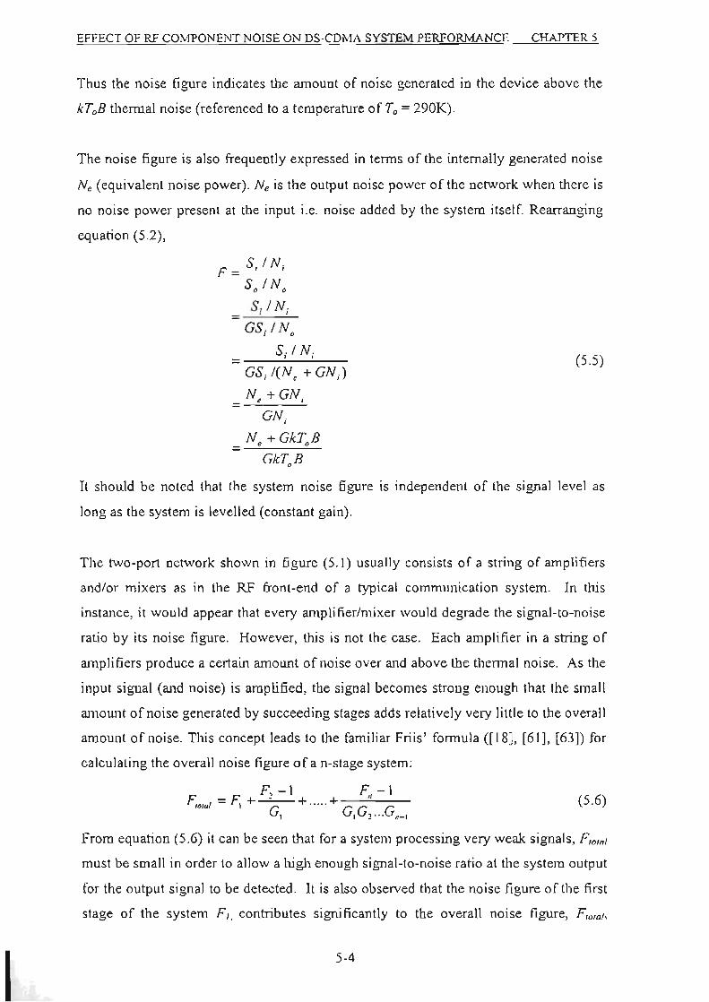
EFFECT OF RF COMPONENT NOISE ON DS-CDMA SYSTEM PERFORMANCE CHAPTER 5
Thus the noise figure indicates the amount of noise generated in the device above the
kT,j3 thermal noise (referenced to a temperature of To = 290K).
The noise figure is also frequently expressed in terms of the internally generated noise
Ne (equivalent noise power). Ne is the output noise power of the network when there is
no noise power present at the input i.e. noise added by the system itself. Rearranging
equation (5.2),
F = S,I N , So I N o
Si I N j =
GS,I N.
= -==---:S,-,-,:-I N,-,,-::. =-:GS, /(N, + GN, )
Ne +GN,
ON;
N, + GkT. B
GkT. B
(5.5)
It should be noted that the system noise figure is independent of the signal level as
long as the system is levelled (constant gain).
The two-port network shown in figure (5.1) usually consists of a string of amplifiers
andlor mixers as in the RF front-end of a typical communication system. In this
instance, it would appear that every amplifier/mixer would degrade the signal-to-noise
ratio by its noise figure. However, this is not the case. Each amplifier in a string of
amplifiers produce a certain amount of noise over and above the thennal noise. As the
input signal (and noise) is amplified, the signal becomes strong enough that the small
amount of noise generated by succeeding stages adds relatively very little to the overall
amount of noise. This concept leads to the fami liar Friis' fomlUla ([18J, [61J, [63]) for
calculating the overall noise figure ofa n-stage system:
F, -I F-I F'()/4' = F. + -' - + ..... + -=---="-=--
G] G] G2 •• . G 11_]
(5.6)
From equation (5.6) it can be seen that for a system processing very weak signals, F,o,al
must be small in order to allow a high enough signal-to-noise ratio at the system output
for the output signal to be detected. It is also observed that the noise figure of the first
stage of the system F I . contributes significantly to the overall noise figure, Flola[,
5·4

EFFECT OF RF COMPONENT NQ ISE ON OS-COMA SYSTEM PERFORMANCE CHAPTER 5
provided the gain G I in this stage is high. Hence it is necessary to have a low-noise
and high-gain device as the first stage of a system processing weak signals.
5.3 System architecture and simulation work
In order to assess the effect that these RF components will have on system
performance, it is necessary to simulate a complete CDMA transmit-receive system.
5.3.1 Transmitter architecture
Figure (5.2) shows the transmitter archi tecture fo r the proposed adapt ive COMA system.
I Data I Spreading Premodulationlpu lse ~
BPSK circuit shaping fill er modulalOr
97.5kbps i i PN Code I
Root raised RF carrier
cosine filte r
4.096MHz 30dBm,2GHz
Fig. 5.2: Transmitter architecture
tr RF
ansmitted signal
The transmitter system was configured as discussed in chapter 4. However, the power
level of the 2GHz RF carrier was chosen to be 30dBm (I W) (not JOdBm as used
previously). The transmitter utilizes a root raised cosine premodulation filter since the
raised-cosine pulse is seen to have a faster spectral relloff than rectangular pulses.
Thus for a channel with a bandwidth wide enough to include the first lobe, transmitting
raised cosine pulses will result in the reception of more power with less pulse
distortion than for rectangular pulses. The receiver baseband filter would also consists
of a similar (matched) root raised cosine filter as utilized in the transmitter.
5.3.2 Receiver architecture
This simulated transmitted signal is then injected into the RF front-end receiver where
downconversion and demodulation are performed. Downconversion to an fF of
68MHz is performed using a mixer. The choice of this particular IF is based on an
adaptive antenna system developed by Virginia Polytechnic Institute and State
University [64]. It is envisaged that a system similar to that used in [64] will be used
for signal digitization and baseband processing. Demodulation is performed on this IF
5-5

EFFECT OF RF COMPONENT NOISE ON DS-CDMA SYSTEM PERFORMANCE CHAPTER 5
signal. Figure (5.3) shows the receiver architecture for the proposed adaptive COMA
system.
Channel noise
RF transmin
s ignal ed
RF channel attcnuator
BPSK ... demodulalor
RF IF Bandpass Bandpass IF
LO
:tE Receiver RF front-end ~,
Basebandlpulse - Despreading r- Received shaping filler circuit data
PN Code
, , , , , , , , , , , , , ,< Si£Tlal digitization and baseband processing stages >'
Fig. 5.3: Receiver architecture
5.3.2.1 Systematic analysis of receiver design
In receiver design, it is often advantageous to have a priori idea of the perfonnance of
each receiver component technology (specifications) before it is integrated. [n order to
assess the effect of internally generated RF component noise on the system, it is
essential that the RF component specifications are known. The specifications of
interest (noise figure and gain) can be traded-off to assess how a required system
specification (such as the bit error rate) can be met. Table (5.1) lists the baseline
specifications for each receiver RF front-end block in the proposed system. The
specifications in table (5.1) are derived from a range of Avantek 's RF and microwaves
product catalogues. The RF LNA data is based on the AFT4231 wideband amplifier.
It has a typical gain and noise figure of 12dB and 3.6dB, respectively over the 2 to
4GHz range. The RF and IF bandpass filters used are based on Avantek's AFP2 1851
and AFP4 1851 broadband YIO bandpass fi lters with maximum insertion loss of
between 6 and 9dB with a 3dB minimum bandwidth of 20 MHz in the 1 to 180Hz
5-6
EFFECT OF RF COMPONENT NOISE ON DS-CDMA SYSTEM PERFORMANCE CHAPTER 5
frequency range. The mixer noise figure is based on Avantek's UMX series mixers
(TFX-72M) with conversion losses varying from 5 to 7dB. The IF amplifier used is
based on the PPA-1043 that has a minimum gain and maximum noise figure of IOdB
and 4dB, respectively over the lOMHz to 1 GHz frequency range.
Receiver Block NF (dB) Gain (dB)
LNA 3 13
RF Bandpass filter , , , -0
Mixer 5 -5
IF Bandpass filter 3 ,
-0
IF ampl ifier 4 10
Table 5.1: Baseline noise figure and gain for proposed receiver RF front-end
The overall noise figure of the baseline system using Friis' equation ([18], [61], [63])
is SA78dB. It should be noted that 0.5 to 2dB tends to be the state of the art range of
noise figures for solid state microwave receivers [18]. Currently, the noise figures of
commercially avai lable receiver front-ends for PCS, CDMA and FM systems produced
by RF Microdevices (e.g. RF9906, RF9936 and RF9986), range from 2.SdB to S.ldB.
From figure (5.3), it can be seen that the 30dBrn RF transmitted signal is directly
coupled to the receiver front-end via an attenuator. The attenuator was included in the
simulation since direct injection of the 30dBm RF signal into the front-end would not
only drive the LNA. mixer and IF amplifier into compression but more importantly.
would exceed the operating power rating of these devices thereby damaging them.
Hence an anenuator with -120dB attenuation was used. Thus the signal power into the
front-end is -90dBm ( lpW or 7.071~V into SOn). The typical minimum and
maximum RF sensitivity of an IS-55 receiver is - IIOdBm and -25dBm. respectively
[65]. Thus the -90dBm signal power level is within the dynamic range or sensitivity
range of typical wireless receivers. Channel noise power of approximately - I OOdBm
was introduced into the receiver RF front-end to establ ish a SNR in the order of IOdB
at the input of the LNA. A link budget analysis perfonned on an an IS·55 system uses
a SNR of 13dB at the input of the receiver [65]. Thus the SNR of IOdB is a reasonable
estimate for which the bit error rate would be detennined after the simulation. It
should be noted that this noise power is va lid over a bandwidth of 24.576MHz which
is the RF bandwidth or RF frequency span used by the ADS software. This bandwidth
S-7

EFFECT OF RF COMPONENT NOISE ON DS-CDMA SYSTEM PERFORMANCE CHAPTER 5
is the reciprocal of the time step or sampling time (TsII!P) used by the software. The
sampling time should be chosen such that Ts1ep < l if,n(max) where f"J(max) is the
highest baseband frequency component. In this instance, / m{max) is the fTequency of
the chipped data (4.096MHz). Each chip was sampled 6 times (T",p ~ 40.69ns). The
sampling time can be reduced but at the expense of a longer simulation run time. The
baseband bandwidth or frequency span (after carrier demodulation) is lZ.Z88rvrHz i.e.
one half of the RF bandwidth.
5.4 BER Measurement methodology
A useful parameter that can be used to gauge the quality of a digital communication
system is the probability of bit error (denoted either as Pe or BER). Most wireless
voice systems can tolerate one bit error in every 1000 bits received (Pe=10·3), before
their perfonnance is deemed unacceptable. Other applications, such as data transfer,
demand a much lower Pe. Typical values of Pe in this instance are 10.8 to 10·\0 for
systems such as Ethemet and token ring networks [65].
ADS has two techniques for the computation of Pe. These are the Monte Carlo and the
Improved Importance Sampling (lIS) ([66]. [67]. [68]) techniques. The Monte Carlo
measurement technique is based on comparing test data (output data stream) to
reference data (input data stream), symbol by symbol. However, a major disadvantage
of th is method is that the number of bits transmitted should be very large for a
statistically significant Pe measurement to be made. The relative variance (VAR) of
the Pe for Ntransmitted bits is:
(I-P) VAR~ e
N.Pe (5.7)
This implies that for a Pe of 10-6, with a relative variance of 0.01, a sample size N of
approximately 108 bits is required.
The probability of error was measured using the IIS technique [66]. [67]. [68]. The
use of this technique is justified over the Monte Carlo technique since it requires a
fewer number of bits to be simulated thereby reducing the simulation run time
considerably. For example, using a QAM system with a Pe of 10-6, a Monte Carlo
simulation requires 108 simulation samples for a relative variance accuracy of 0.01.
5-8
EFFECT OF RF COMPONENT NOISE ON DS-CDMA SYSTEM PERFORMANCE CHAPTER 5
For the ITS simulation, only 800 samples are needed for a similar accuracy [66].
However, the bit error rate sink in ADS utilizing this lIS technique, does not take into
account external noise in the computation of the bit error rate. Instead, the user is
required to have a priori knowledge of this infonnation and express it in tenns of the
noise bandwidth, variance and ratio of energy per bit to noise power spectral density
(EIINo). Alternatively. the Monte Carlo method computes EtlNo using the formulae in
equations (5.8) and (5.9) below. This value can then be used as one of tht: input
parameters to the lIS measurement sink.
The Pe or BER is related to the signal-ta-noise ratio (SNR) and the ratio of energy per
symbol to the noise power spectral density (Et/No). Both the SNR and EtlNo were
computed at the output of the IF amplifier in figure (5.3) i.e. before demodulation.
ADS uses the RF bandwidth (l /Ts,ep) for the computation of these parameters. The
following formulae are used in the simulation for the calculation of Eb and No :
Where Eb = Energy per bit
PESREF = source power in the reference RF signal (output of IF amplifier)
Tb = bit time
(5.8)
(5.9)
Where No = one-sided power spectral density of the band limited white noise in WlHz
P ENREF = noise signal power at output of IF amplifier
Ts1ep = simulation time step
or in terms of E,fNo.
P SNR = ESREF
PENREF
Eb PESREFTb - = -;:-"='-;;:-"N o P ENREF Ts1ep
Tb = SNR--
Tsrep
Thus, with knowledge of the SNR value, the EJ No value can be calculated.
(5.10)
(5. 11 )
In [57] the
processing gain (Gp) is related to the SNR and EJNo value by the following equation,
Eb N o = SNR.xGp (5.12)
5-9

EFFECT OF RF COMPONENT NOISE ON DS-CDMA SYSTEM PERFORMANCE CHAPTER 5
[n order to be consistent wi th the standard definition of EJNQ in tenns of the
processing gain [57], it is appropriate that equation (5. 11 ) be scaled by a factor of 6
(7.782dB). This effectively reduces the simulation bandwidth from 24.576MHz to the
spread bandwidth of 4.096MHz. A further discussion on this scaling and other ADS
simulation issues are provided in appendix AA.
5.5 Simulation results and analysis
Simulation results for different front-end scenarios are shown in figures (5.4) to (5.20).
The lookup tab le (table (5.2» provides a quick reference to these simulat ion plots,
showing varied and constant parameters.
Figure number LNA NF (dB) LN A gain (dB) Mixer NF (dB)
5.4 5.8 3 3 13 5
(variable parameter)
5.9 5.13 3 13 13 5
(variable parameter)
5. 14 - 5. 18 3 13 5 15
(variable parameter)
5. 19 and 5.20 Comparison of system with LNA (LNA NF 5- 15
~ 3dB and LNA gain ~ I3dB) and without (variable parameter)
LNA
. . Table 5.2. Lookup table showmg constant and varied parameters of figures (5.4)
to (5.20)
The obvious trend from these results is that an increase in component noise figure
causes the BER, Et/No and SNR to decrease, and vice-versa. Also, an increase in
component gain (up to the gain that produces device saturation and compression)
causes a decrease in BER, EIINo and SNR. It should be noted that the SNR values are
computed at the output of the IF amplifier i.e. before demodulation.
From figure (5.4), LNA gain in the range 3dB to 13 dB produce BERs between
7.6xlO·12 and 7.5xlO-3. Et/No values range between 13 .9dB and 20.8dB for th is range
of LNA gain (figure (5.5». A SNR value of - 2.5dB was obtained for the lower limit
5-10

EFFECT OF RF COMPONENT NOISE ON DS-CDMA SYSTEM PERFORMA CE CHAPTER 5
of LNA gain (3dB) while a SNR of 4.4dB was obtained for a 13dB upper limit LNA
gain (figure (5.6)).
I.E-02 , I I.E-04
= I.E-06 ~
= 1.E-OS
1.E-IO
1"'-,
"'" " I.E- J2
3 4 5 6 7 g 9 10 11 12 13
LNA Ga in (dB)
Fig. 5.4: LNA gain versus BER (LNA NF=3dB)
21 2.
~ ,. ...--
= 18 " -• 11 ----~ Z 16 .."
'" " 14 "7 13
3 4 S 6 7 8 9 10 1I 12 \3
LNA gain (dB)
Fig. 5.5: LNA gain versus E"tN. (LNA NF~3dB)
, 4
~ 3
" 2
" . .---- ,
'" z • ,
'" ., -2 -3
3 4 5 6 7 8 9 10 11 12 13
LNA gain (dB)
Fig. 5.6: LNA gain versus SNR (LNA NF~3dB)
5-1 I

EFFEcr OF RF COMPONENT NOISE ON OS·COMA SYSTEM PERFORMANCE CHAPTER 5
I.E·02
I.E·04
0: I.E·06
'" = LE·OB
I.E·IO
I.E· 12 " " ~
13 14 15 16 17 18 19 20 21
E"IN, (dB)
Fig. 5.7: Et/N. versus BER for varying LNA gain (3 to I3dB) (LNA NF~3dB)
I .E-02
I.E·04
" I.E·06 ~
'" = 1.E-08
1.E·IQ
f'.. \ ...
I.E-12
-3 -2 -\ 0 2 3 4 5
SN R (dB)
Fig. 5.8: SNR versus BER for varying LNA gain (3 to I3dB) (LNA NF~3dB)
Figure (5.9) shows a plot of LNA noise fi gure versus BER where it can be seen that for
a LNA gain of 13dB and an unreasonably high noise figure of 13dB, the BER is
12.9x I0·' while the BER is 7.6xlO·12 for a typical noise figure of 3dB. The Et/N.
values range between 13dB and 20.8dB for noise figures between 3dB and l3dB
(fi gure (5.10)). The SNR degrades from 4.4dB to - 3.4dB with an increase in LNA
noise fi gure from 3dB to 13dB (fi gure (5. 11 ».
5· 12

EFFECT OF RF COMPONENT NOISE ON OS-COMA SYSTEM PERFORMANCE CHAPTER 5
woo I I.E-02
I.E-04 ~ ;aJ I .E-06 =
\ .E.Q8
I.E·IQ
I.E-12 V
I I I .-'
¥ .
J 4 5 6 7 8 9 10 11 12 13
LNA noise figure (dB)
Fig. 5.9: LNA noise figure versus BER (LNA gain~13dBl
21
2 • 19
=- 18 :E ]7
~ 16 _ 15
14
Jl 12
,
....... .......,
-
r-....
3 4 5 6 7 8 9 10 11 12 13
LNA noist figure (dB)
Fig. 5.10: LNA noise figure versus E"IN. (LNA gain~13dBl
, 4
3
.. 2 ", 1
" . Z '" -1
· 2 -3 -4
r--. ......., ---.,
-
~ 3 4 5 6 7 8 9 \0 \1 12 13
LNA noise figure (dB)
Fig. 5.11: LNA noise figure versus SNR(LNA gain=13dB)
5-1 3
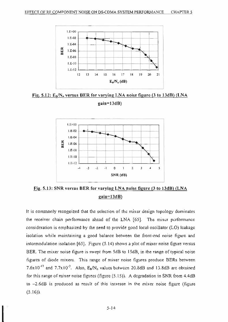
EFFECT OF RF COMPONENT NOISE ON OS-COMA SYSTEM PERFORMANCE CHAPTER 5
I .E+OO
I.E-02
I.E-04
'" I .E-06 '" '" I.E-08
I.E·10
-.....
"" ,
" I.E·12 ..
12 13 14 15 16 17 18 19 20 21
["IN, (dB)
Fig. 5.12 : E,,!N. versus BER for varying LNA noise figure (3 to 13dB) (LNA
gain~l3dB)
LE+oo
1.&02 I I .E.Q4
'" I.E-06 '" " I.E-08 , ..
I.E·IO . I.E·12
I I. -4 -3 -2 -\ 0 2 J 4 5
SNR (dB)
Fig. 5.13: SNR versus BER for varying LNA noise figure (3 to 13dB) (LNA
gain~l3dB)
It is commonly recognized that the selection of the mixer design topology dominates
the receiver chain perfonnance ahead of the LNA [65]. The mixer perfonnance
consideration is emphasized by the need to provide good local oscillator (LO) leakage
isolation whi le maintaining a good balance between the front-end noise figure and
intermodulation isolation [65]. Figure (5. 14) shows a plot of mixer noise figure versus
BER. The mixer noise figure is swept from SdB to lSdB, in the range of typical noise
figures of diode mixers. This range of mixer noise figures produce BERs between
7.6xI0·" and 7.7xI0·'. Also, E,,!N. values between 20.8dB and 13.8dB are obtained
for this range of mixer noise figures (figure (5.15)). A degradation in SNR from 4.4dB
to - 2.6dB is produced as result of this increase in the mixer noise figure (figure
(5.16)).
5-14
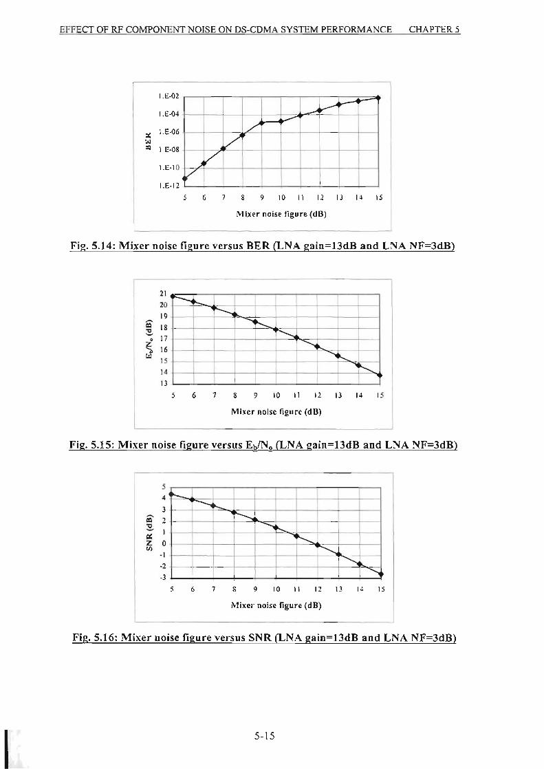
EFFECf OF RF COMPONENT NOISE ON DS-CDMA SYSTEM PERFORMANCE CHAPTER 5
J.E-02
I.E.(l4 I V
" I .E-06
'" = I .E.oS
l.E·IO
/
V V
V I.E-12
5 6 7 8 9 10 11 12 13 14 IS
Mixer noise figure (dB)
Fig. 5.14: Mixer noise figure versus BER (LNA gain=13dB and LNA NF=3dB)
21
20
I'
=- IS ~ i 17 -,. 16 ~ IS
I' 13
I -..., ~ ---.,
" r---r---
5 6 7 8 9 10 I1 12 13 14 15
Mixer noise figure (dB)
Fig. 5.15: Mixer noise figure versus EtJN. (LNA gain=13dB and LNA NF=3dB)
, • , 3
iO 2 ""---, ~ - 1
" Z 0 r---'" -1
-2
, :":>
-3
5 6 7 8 9 10 11 12 \3 14 IS
Mixer noise figure (dB)
Fig. 5.1 6: Mixer noise figure versus SNR (LNA gain=13dB and LNA NF=3dB)
5-15

EFFECT OF RF COMPONENT NOISE ON DS·CDMA SYSTEM PERFORMANCE CHAPTER 5
I ::: ::z:: I.E-06
'" ::: \ .E-OS
l.E· 10
LE· 12
n \4
... 1
"'\. '.
" 15 16 \7 18 19 20 11
E,IN. (dB)
Fig. 5.17: E.JNo versus BER for varying mixer noise figure (5 to 15dB) (LNA
gain~\3dB and LNA NF~3dB)
1.£-02
LE-04
" I.E-06 "' '" = i .E-08
I.E·l0
I'.. "\ ..
I.E·1 2
·3 ., . \ o 2 3 4 , SNR (dB)
Fig. 5.18: SNR versus HER for varying mixer noise figure (5 to 15dB) (LNA gain- 13dB and LNA NF-3dB)
As previously mentioned, the mixer noise figure is swept from 5dB to l SdB. in the
range of typical noise fi gures of diode mixers. Diode mixers are passive components
and consequently exhibit conversion loss. Typical conversion losses of diode mixers
are between 6dB to 9dB [69]. This loss has a number of consequences: the greater the
loss, the higher the noise of the system, and the more amplification is needed. High
loss also indirectly leads to distortion because of high signals that result from the
additional preamplifier gain required to compensate for this loss. It also adds to the
cost of the system since the low-noise amplifier stages are usually expensive [65]. In a
passive mixer, the noise figure is usually equal to, or only a few tenths of one decibel
above. the conversion loss. In this sense, the mixer behaves as if it were an attenuator
having a temperature equal to or slightly above the ambient. Diode mixers are the
highest-frequency low-noise microwave components in existence: at high frequencies
5· 16
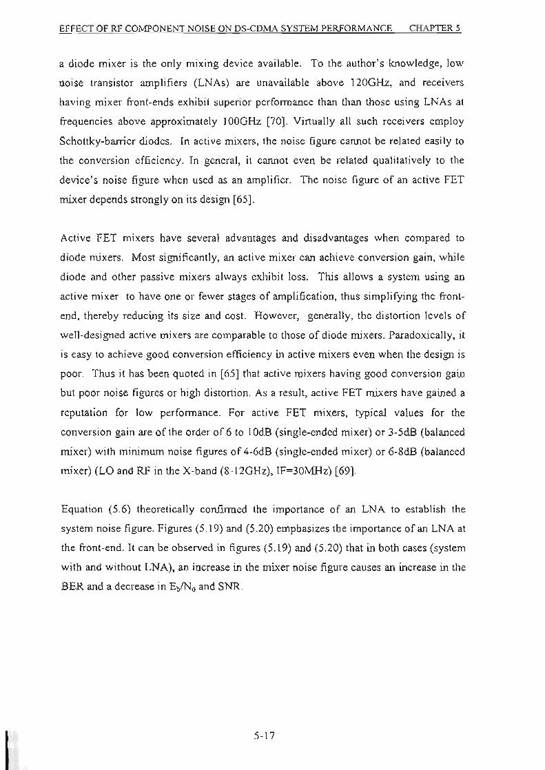
EFFECT OF RF COMPONENT NOISE ON DS-CDMA SYSTEM PERFORMANCE CHAPTER 5
a diode mixer is the only mixing device available. To the author's knowledge, low
noise transistor amplifiers (LNAs) are unavailable above 120GHz, and receivers
having mixer front-ends exhibit superior perfonnance than than those using LNAs at
frequencies above approximately lOOGHz [70]. Virtually all such receivers employ
Schottky-barrier diodes. In active mixers, the noise figure CalIDot be related easily to
the conversion efficiency. In general, it C31mot even be related qualitatively to the
device's noise figure when used as an amplifier. The noise figure of an active FET
mixer depends strongly on its design [65].
Active FET mixers have several advantages and disadvantages when compared to
diode mixers. Most significantly, an active mixer can achieve conversion gain, while
diode and other passive mixers always exhibit loss. This allows a system using an
active mixer to have one or fewer stages of amplification, thus simplifying the fTont
end, thereby reducing its size and cost. However, generally, the distortion levels of
well-designed active mixers are comparable to those of diode mixers. Paradoxically, it
is easy to achieve good conversion efficiency in active mixers even when the design is
poor. Thus it has been quoted in [65} that active mixers having good conversion gain
but poor noise figures or high distortion. As a result, active FET mixers have gained a
reputation for low perfonnance. For active FET mixers, typical values for the
conversion gain are of the order of 6 to lOdE (single-ended mixer) or 3-5dB (balanced
mixer) with minimum noise figures of 4-6dB (single-ended mixer) or 6-8dB (balanced
mixer) (LO and RF in the X-band (S-12GHz). lF~30MHz) [69] .
Equation (5.6) theoretically confirmed the importance of an LNA to establish the
system noise figure. Figures (5.19) and (5.20) emphasizes the importance of an LNA at
the front-end. It can be observed in figures (5.19) and (5.20) that in both cases (system
with and without LNA), an increase in the mixer noise figure causes an increase in the
BER and a decrease in EtlNo and SNR.
5-17

EFFECT OF RF COMPONENT NOISE ON DS-CDMA SYSTEM PERFORMANCE CHAPTER 5
I.E+OO
t .E-02
I.E-04
" " I.E-06 ~
\.E'()8
LE-IQ
+ + T t T T T T ! ! ! I /"
V I.E·12
5 6 7 8 9 10 11 12 13 14 IS
Miller noise figure (dB)
I-+--With LNA (Gain I3dB and NF-3d(3) ____ Without LNA I Fig. 5.19: Comparison of mixer noise figure versus HER for system with and
witbout LNA
= '" • Z ">
'"
21
18 IS
12 -- r--9 6
3
0 I I I I i ! I
5 6 7 8 9 10 11 12 13 14 15
MIxer noise fi gure (dB)
, 2
-I ~ ~
-4 :=. -, " Z - 10 VI
-13
-16
I-+-With LNA (Gain-13dB and NF-3dB) __ Withoul LNA I
Fig. 5.20: Comparison of mixer noise figure versus E.,tNo and SNR for system
with and without LNA
For the proposed system utilizing an LNA, the BERs are between 7.7xIO-3 and
7.6x l O-12 fo r mixer noise figures (or conversion losses) in the range SdB to 15dB.
However. without an LNA , the BERs range from 2.8xlO·z to 2.7xIO-1 for the same
range of mixer noise figures. For the proposed system (utilizing a mixer with 5dB
conversion loss/noise figure), Et/No and SNR improvements of 9.S3dB are obtained
over the same system without an LNA. Also Ei/No and SNR improvements in the
range 9.53dB to 12.51dB are obtained for mixer noise figures from 5dB to 15dB.
An expressIOn for SNR improvement, which quantifies how much the SNR is
improved by adding an LNA between the antenna and the radio, is derived in [57].
Since CDMA has reverse-link power control, the improvement in SNR is manifested
in the reduction of mobile transmit power. This is intuitive because if there is an
5-1 8

EFFECT OF RF COMPONENT NOISE ON OS·COMA SYSTEM PERFORMANCE CHAPTER 5
improvement in SNR, reverse power control would command the mobile to power
down so that the mobile transmit power is just enough to achieve the desired link SNR.
As a result, the battery life-span of the mobile unit is increased.
5.6 Concluding remarks
The impact of internally generated RF component noise on a DS-COMA system (via
simulation) was investigated. The conclusions of this investigation are clear: Firstly.
the importance of an LNA at the receiver front-end was established. For the proposed
system (processing gain of 42) the use of an LNA yielded a BER below 10-11 while
without an LNA the BER was more significant (2.8x1O-\ Secondly, it can be
concluded that the use of commercially available RF components in the front-end do
not cause severe BER degradation in a single-user DS-CDMA system. In a worst
case, highly improbable scenario, an LNA gain as low as 3dB and noise figure as high
as 13dB produce BERs of7.5xlO-3 and 12.9xIO-3, respectively for a modest processing
gain of42.
Thus far a system block diagram was established to ensure demodulation of a very
weak - 90dBm contant-level signal i.e. disregarding a change in the received signal
strength. A change in the received signal strength can cause distortion to a complete
wiping off and loss of the infonnation. Variations in signal strength occurs when the
receiver is a mobile. Large buildings and underpasses will greatly attenuate the signal.
in reality, such signal strength variations require the receiver to incorporate automatic
signal-level control or automatic gain control (AGC) in either the RF LNA or the [f
amplifer. In the case of the receiver being a base station, this near-far effect IS
eliminated by power control (which is synonymous to AGC) ([I] , [57], [60]).
5·19

IMPACf OF LO GENERA TEO PHASE NOISE ON OS-COMA PERFORMANCE CHAPTER 6
CHAPTER 6
THE IMPACT OF LOCAL OSCILLATOR GENERATED PHASE
NOISE ON DS-CDMA PERFORMANCE
6.1 Introduction
The local oscillator (LO) is often considered as being part of the mixer and is a
common building block in wireless communication systems. since it provides precise
reference frequencies for modulation/demodulation and frequency conversion.
Often the noise induced by the LO is classified as internally generated mixer noise.
However, the LO induces amplitude (AM) noise, phase noise and spurious signals. An
ideal oscillator or frequency synthesizer will produce a perfectly pure sinusoidal
signal. The amplitude, phase and frequency of the source would not change under
varying loading, bias or temperature conditions. However, such an ideal circuit is
impossible to realize in practice. Therefore performance measures such as the
amplitude noise, phase noise and spurious responses are used to characterize the
deviation from the ideal.
The focus of this chapter is on the impact of LO generated phase noise on DS-CDMA
performance. However, LO spurious signals and amplitude noise are briefly
discussed.
6.2 Internally generated spurious signals
Local oscillators also cause spurious signals which are unwanted frequency
components in the LO signal that are converted to the IF or simply leak through the
mixer into the IF circuit. These spurious signals are applied to the mixer along with the
LO and, depending on their frequencies, may be converted to a frequency within the IF
band. The most serious problems arise when the spurious signals are within the RF
6-1

IMPACT OF LO GENERATED PHASE NOISE ON DS·CDMA PERFORMANCE CHAPTER 6
passbands; in this case the downconverted spurious signals may be much stronger than
the RF signals. For example, consider a mixer having an RF input of - IOOdB, and a
LO having an RF frequency spurious signal that is 60dB below the LO signaL
Assuming a conversion loss of 7dB, the [F output level of the desired signal is
- 107dB. If the LO level is 10dBm, the spurious signal level is - 50dBm. With 7dB
conversion loss plus 20dB rejection due to mixer balance, the spurious IF signal is
- 77dBm or 30 dB above the desired output.
The source of such "spurs" is the frequency synthesizer used to generate the LO.
A voiding spurious signals requires careful selection of frequencies not only in the
receiver front-end, but also in the LO synthesizer. Any frequency used in the
synthesizer represents a potential spurious signal in the LO output. The use of a high
IF frequency will allow effective LO filtering. The fF amplifier bandwidth should be
kept as narrow as possible, so that spurs outside the IF passband are not amplified to
the level where they might saturate the fF amplifier or generate intermodulation
components.
6.3 Amplitude (AM) uoise
AM noise which is generated by the LO source is injected into the mixer along with
the LO signal. This noise is severe when the LO signal is generated at a low level and
amplified.
A mixer's LO signal can be generated in many ways. The simplest is to use some type
of osci llator operating directly at the LO frequency. In some cases, the LO signal is
generated initially at a subharmoruc of the desired LO frequency and multiplied to the
desired frequency. The frequency multiplier often requires a high input level, and it is
necessary to amplify the original subhamlonic signal substantially. Amplifying the LO
adds a certain amount of noise. This noise is AM noise; it consists of variations in the
amplitude of the LO signal and can be treated as an additive noise process. When the
noisy LO signal is app lied to the mixer, its AM noise components at the RF and image
frequencies are downconverted and appear at the IF port just as if they had been
applied to the RF input. Therefore, the mixer noise temperature (or noise figure) is
increased by an amount, depending on the type of mixer used, may be as high as the
6·2

IMPACf OF LO GENERATED PHASE NOISE ON DS·CDMA PERFORMANCE CHAPTER 6
La noise temperature. Ifno measures are taken to eliminate the La noise, the increase
in the mixer 's noise temperature may be very great.
The AM La noise can be reduced by straight-forward techniques to a level where it is
insignificant. The IF frequency is picked up high enough so that the RP and image
frequencies are well separated from the La frequency, so the noise at these frequencies
can be removed effectively by filtering. The fF frequency should typically be at least
5% to 10% of the La frequency if it is expected that AM noise will have to be
removed by filtering. This may require a trade-off with IF ampli fier noise temperature,
since amplifier noise temperatures generally rise with frequency.
The general fonn of the expression for the output wave from a noisy oscillator can be
written as
V(t)~ [vo H(t)~os [2iifot+I'(t)1
wherelo = nominal oscillation frequency
Vo = nominal oscillation amplitude
E(I) = fluctuations in amplitude
rKI) = fluctuations in phase
(6.1 )
Equation (6.1) indicates there is a concentration of noise power surrounding the RF
local oscillator signal. A typical spectral distribution of such a signal is shown in
figure (6.1).
{, • Frequency
Fig. 6.1: Noise spectrum of a RF local oscillator signal (from 171])
In general, both the AM noise and FM or phase noise, &(1) and r/(I), respectively are
present, accounting for the lack of symmetry in the envelope of the spectrum. The AM
6-3

IMPACT Of LO GENERATED PHASE NOISE ON OS-COMA PERfORMANCE CHAPTER 6
noise component in this instance is negligible when compared to the phase/frequency
noise component [72]. Thus it is often neglected in the analysis of phase noise.
6.3.1 Analysis
6.3.1.1 Sinusoidal modulation
With the phase noise component~(I)=O , equation (6. 1) can be rewritten as
V(f} ; [vo +£(f})::os(21ifof)
Letting E(r) = Eo cos(ro .. m t } , equation (6.2) can be written as
V( r) = lvo + E 0 cos(ro ANI} Jcos{O) of)
= v 0 cos(ro 0 1) + & 0 cos(ro AN t )cos(ro ot )
=Vo COS(Wo fJ+ E; ~OS((J)o +(r)AN)I + COS((J)o -roAN)']
(6.2)
(6.3)
where ro AN :: 2njAN is angular frequency of modulation and roD =2rr./o is the angular
osci llation frequency.
The spectrum of a sinusoidally amplitude-modulated sinuso idal signal consists of three
unmodulated sinusoidal signals located at three frequencies: Io,Io-/AN,Io+ fAN (figure
(6.2))
v' •
£ 2 , £ 2 " 4 4
f,
Fig. 6.2: Spectrum of sinusoidallv amplitude-modulated sinusoidal signal
The vectorial representation of this consists of a vector of amplitude Vo rotating at (00
and two vectors of amplitude &012 rotating at (00 + roAN and roo - roAN, whose resultant
is collinear with V, (figure (6.3)).
6-4

IMPACT OF LO GENERATED PHASE NO ISE ON OS-COMA PERFORMANCE CHAPTER 6
AM vector I
v
o 2n1,;
Fig. 6.3: Vector representation of sinusoidally amplitude-modulated sinusoidal
signal
The maximum signal power is:
p.~ = ~, [v. +{ E; )]' (6.4)
The minimum signal power is:
Pm" = ::' [v. _{ E; )]' (6.5)
The fluctuation in power is then
(6.6)
6.3.1.2 Modulation bv noise
By assuming that the modulating signal is noise of spectral density S(fANJ , the spectrum
can be broken down into elementary components separated by differences in frequency
of/m and each located within a frequency band Llf(ligure (6.4)).
Com!r
Upper i,C!coond
Fig. 6.4: Representation of a wave modulated by noise (from 169))
6-5

IMPACT OF LO GENERATED PHASE NOISE ON OS-COMA PERFORMANCE CHAPTER 6
The nOIse power can then be represented in each frequency band by a sinusoidal
generator with a frequency equal to that of the centre of the band concerned and with
an amplitude proportional to ~2S(/tN )6/ (the proportionality coefficient takes
account of the modulation of the oscillator by the noise). The general spectrum will
have the form shown in figures (6.2) and (6.3), but there wi ll he many vectors rotating
with angular velocities distributed uniformly in a continuum. The above relationships
are then valid for each equivalent generator and thus for the entire noise modulation.
Measurement of AM noise is generally ach ieved by applying the complete spectrum to
a square-law detector of sensitivity S which produces fluctuations in steady voltage
corresponding to the fluctuations of power produced by the noise. The voltage
fluctuations then undergo standard low-frequency treatment for noise measurement. If
S = LlVI.:1P and if an index for AM noise is defined by:
M . . d .:N"o"is",e,:-"p-=o-,-\\-='ec,r:..:i"Il:..:'"h"e-=S.::id"e:.:b"o",ll-=d=-s A IIOlse 1II ex = -Power ill the carrier
(6.7)
[(AV'ff I SP,,)']
or AM noise index = 10 log,o 4 (6.8)
in dB with respect to the carner (dBc). The index is given in dBcHz-1•
6.4 Phase noise
Present-day technology demands signal sources with better frequency stabi lity for
systems such as doppler radars, data communication links and multichannel receivers.
Characterizing the randomness of frequency stability is a common requirement for all
these systems. Phase noise is the term most widely used to describe this characterist ic.
The analysis of the effect of phase noise in OFDM (Orthogonal Frequency Division
Multiplexing) systems ([73J, [74]) and a MC-CDMA (Multicarrier CDMA) system
([75]) has been presented. In [75J, an analytical procedure was developed to evaluate
the impact of carrier frequency offset and phase noise on the performance of a MC
CDMA system. The investigation in [75] concluded that phase noise introduces a
spurious phase rotation on the useful signal and also introduces interchannel
interference which is primarily responsible for perfomlance degradation. It has also
been concluded in [75] that MC-CDMA is very sensitive to the signal distortion
6-6
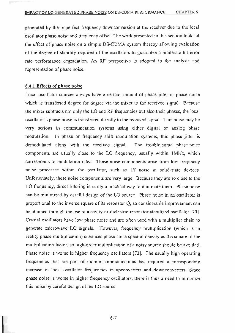
IMPACf OF LO GENERATED PHASE NOISE 0 OS-COMA PERFORMANCE CHAPTER 6
generated by the imperfect frequency downconversion at the receiver due to the local
oscillator phase noise and frequency offset. The work presented in this section looks at
the effect of phase noise on a simple DS-CDMA system thereby allowing evaluation
of the degree of stability required of the oscillators to guarantee a moderate bit error
rate performance degradation. An RF perspective is adopted in the analysis and
representation of phase noise.
6.4.1 Effects of phase noise
Local oscillator sources always have a certain amount of phase jitter or phase noise
which is transferred degree for degree via the mixer to the received signal. Because
the mixer subtracts not only the LO and RF frequencies but also their phases, the local
oscillator's phase noise is transferred directly to the received signal. This noise may be
very serious in communication systems using either digital or analog phase
modulation. In phase or frequency shift modulation systems, this phase jitter is
demodulated along with the received signal. The trouble-some phase-noise
components are usually close to the LO frequency, usually within IMHz, which
corresponds to modulation rates. These noise components arise from low frequency
noise processes within the oscillator, such as l / f noise in sol id-state devices.
Unfortunately, these noise components are very large. Because they are so close to the
LO frequency, direct filtering is rarely a practical way to eliminate them. Phase noise
can be minimized by careful design of the LO source. Phase noise in an osci llator is
proportional to the inverse square of its resonator Q, so considerable improvement can
be attained through the use ora cavity-or-dielectric-resonator-stabilized oscillator [70].
Crystal oscillators have low phase noise and are often used with a multiplier chain to
generate microwave LO signals. However, frequency multiplication (which is in
reality phase multiplication) enhances phase noise spectral density as the square of the
multiplication factor, so high-order multiplication of a noisy source should be avoided.
Phase noise is worse in higher frequency oscillators [72]. The usually high operating
frequencies that are part of mobile communications has required a corresponding
mcrease In local oscillator frequencies in upconverters and downconverters. Since
phase noise is worse in higher frequency oscillators, there is thus a need to minimize
this noise by careful design of the LO source.
6-7

IMPACT OF LO GENERA TEO PHASE NOISE ON OS-COMA PERFORMANCE CHAPTER 6
The effects of receiver-LO phase noise are understood by considering the process of
reciprocal mixing. This is an effect that occurs in all mixers, yet despite its name,
reciprocal mixing is a LO, not a mixer, problem. The modulation on the mixer output
(IF) is the combined modulations of the inputs. This means that modulating a
receiver's local oscillator is indistinguishable from using a clean local oscillator and
having the same modulation present on all incoming signals. The noise components of
the LO arc extra LO signals that arc: offset from the carrier [requt:ncy. Each of them
mixes other signals that are appropriately offset from the LO carrier into the receiver's
IF. Noise is the sum of an infinite number of infinitesimal components spread over a
range of frequencies, so the signal it mixes into the IF are spread into an in.finite
number of small replicas, all at different frequencies. This amounts to scrambling
these other signals into noise. It is tedious to look at the effects of receiver LO phase
noise this way. The concept of reciprocal mixing provides an easier alternative that
gives accurate results.
A poor oscillator can have significant noise side bands extending out many tens of
kilohertz on either side of its carrier. This is the same, as far as the signals in the
receiver IF are concerned, as if the LO was clean and every signal entering the mixer
RF input had these noise sidebands. Not only will the wanted signal (and its noise
sidebands) be received, but the noise sidebands added by the LO to signals near, but
outside, the receiver 's IF passband wi ll overlap it. In a multi-user system, each of
many signals present will add its set of noise sidebands. The effect is cumulative.
This produces the appearance of a high background-noise level on the spectrum band.
Figure (6.5) illustrates this effect of phase noise in the receiver LO.
6-8

IMPACT Qf LO GENERATED PHASE NOISE ON DS-CDMA PERFORMANCE C HAPTER 6
Amplitude
Receiver LO phase noise
Amplitude
frequency
Reciprocal mixing
Amplitude D
-L ~
~ Frequency
Wanted signal
Apparent h igh noise level
~ Frequency
Wanted signal
Fig. 6.5: Illustration of the effects of phase noise in the receiver LO
Thus, the phase noise is one of the limi ting factors on dete rmining how closely spaced
(in the frequency domain) two conununication channels can be.
6.4.2 Phase noise analysis and representation
In sect ion (6.3) it was mentioned that the local u :Sl,;illalor spectrum consists of both
amplitude (AM) and FM or phase noise that accounted for the lack of symmetry in the
envelope of the spectrum. The AM portion of the signal is typically smaller than the
FM portion and is usually neglected in the analysis/calculat ion of phase noise. The
reason for this is that the oscillator output is often fed into some form of limiter that
strips off AM components [72]. This is analogous to the function of the limiting IF
amplifier in a FM receiver that removes any AM on incoming signals. The limiter is
like a circuit that converts the signal to logic levels. For example. a diode ring mixer
may be driven by a sine~wave LO of moderate power, yet this signal drives the diodes
6-9
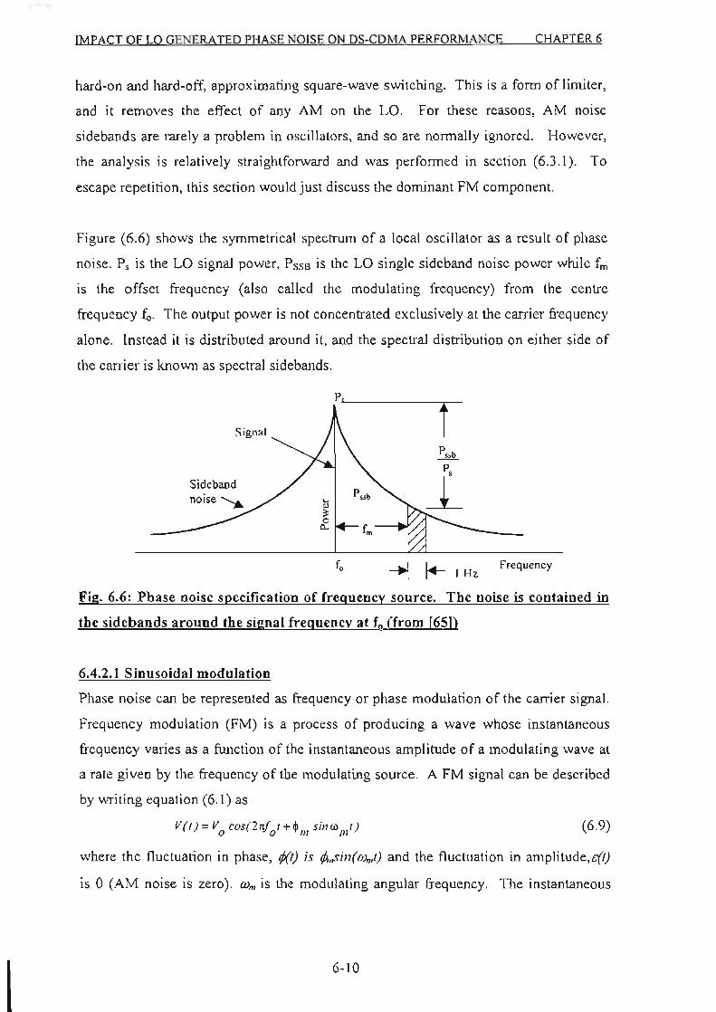
IMPACT OF LO GENERATED PHASE NO ISE ON DS-CDMA PERFORMANCE CHAPTER 6
hard-on and hard-off, approximating square-wave switching. This is a fonn of iimiter,
and it removes the effect of any AM on the LO. For these reasons, AM noise
sidebands are rarely a problem in oscillators, and so are nom1ally ignored. However,
the analysis is relatively straightforward and was performed in section (6.3.1). To
escape repetition, this section would just discuss the dominant FM component.
Figure (6.6) shows the symmetrical spectrum of a local oscillator as a result of phase
noise. Ps is the LO signal power, PSSB is the LO single sideband noise power while fm
is the offset frequency (also called the modulat ing frequency) from the centre
frequency fo. The output power is not concentrated exclusively at the carrier frequency
alone. lnstead it is distributed around it, and the spectral distribution on either side of
the carrier is known as spectral sidebands.
Signal
Sideband noise .........
P~. ____ .--
t
fo --..j f4- I Hz Frequency
Fig. 6.6: Phase noise specification of frequcncv source. The noise is contained in
the sidebands around the signal frequency at fo (from 1651)
6.4.2.1 Sinusoidal modulation
Phase noise can be represented as frequency or phase modulation of the carrier signal.
Frequency modulation (FM) is a process of producing a wave whose instantaneous
frequency varies as a function of the instantaneous amplitude of a modulating wave at
a rate given by the frequency of the modulating source. A FM signal can be described
by writing equation (6.1) as
(6.9)
where the fluctuation in phase, tXtJ is tfJ,,,sin( !Oml} and the fluctuation in amplitude,c{t}
is 0 (AM noise is zero). !tJm is the modulating angular frequency. The instantaneous
6-10
IMPACT OF LO GENERATED PHASE NOISE ON DS·CDMA PERFORMANCE CHAPTER 6
angular frequency cv is obtained by taking the time derivative of the cosine terms of
equation (6.9):
W=!i...(27r.j t+$ silllV l) df 0 111 m
'" 2nfo +wm$m cos2n/",1
or in terms of the instantaneous frequency f,
I f:-oo
2n
:::fo + Im$m cos2n/",t
The frequency variation Llfis given by
6f:f -fo
=$m1m cosh/mt
so that the maximum frequency variation Llf",a;:: is
ll/ mIJ,% = d; ",I".
(6. 10)
(6.11)
(6.12)
(6.13)
4fmnx is t.he maximum swing of the carrier from its mean or nominal frequency.lo.
Hence '" = ll/ ... w: '+'111 I", (6.14)
rAn is known as the peak phase deviation or modulation index. Expanding equation
(6.9) gives
(6.15)
If the modulation factor is small (~,,« l or rAil « rrJ2) as in the case of noise and
narrowband FM),
cos(ljI", 5iIl0)",I)-; 1
hence
v ( t ) = V" cost (iJ ,,1) - V,,1jI '" sill( (iJ "r) sin( (j) ",t)
V~. V ~ :: v" cos(w"t)--'-cos(ro" - OO",)f+~COS(OJo + OJm)t
2 2 (6.16)
V ll/: V AI =VoCOS(OJol)- 0 m .... cos(OJo-Wm)l+ 0 Mlltcos(wo+com)t
2f. 2/.
Equation (6. 16) indicates that the spectrum ofa narrowband FM wave consists of the
carrier plus two components, one on each side of the carrier (figure (6.7».
6·11

IMPACT Of LO GENERATED PHASE NOISE ON OS-COMA PERfORMANCE CHAPTER 6
R
{,,+/'" f
Fig. 6.7: Spect rum and vector representation of a FM wave
Thus, as for an AM signal , a FM signal with a small modulation factor is the sum of
three sinusoidal signals located at frequencies /0, /o-/m. Jo+/m (figure (6.7». In this
sense, narrowband FM is equivalent to AM and cannot be distinguished from it by test
equipment that is not capable of identifying the phase of a signal, such as spectrum
analyzers. However, it is important in system evaluation and in measurement of
spurious outputs and noise to distinguish between AM and FM waves: in the case of
AM, the carrier envelope varies with the modulating signal. whereas the frequency of
the AM wave remains unchanged; in FM, the carrier amplitude is constant, and the
carrier instantaneous frequency varies with the modulating signal. However, the signal
for which the frequency is lowest is in phase opposition to that for which the frequency
is highest. From the vectorial representation, the carrier of amplitude Vo rotates at the
angular velocity 000 , while two vectors of amplitude Ll/md 2/m rotate at angular
velocities 000 + OOm and Wo - OOm with an initial phase difference of 1t. They thus give a
resultant vector RI perpendicular to the carrier. The phase fluctuation LJ~is given by:
(6. 17)
R ' P 641",IU 2 '" lWU; := ~:= max FM noise power in sidebands / Po
Vo Po (6.18)
and thus [69] (6.19)
where Il./eff is the effective or RMS frequency deviation, Po is the power of the carrierlo
and P1SB is the double sideband noise power.
6.4.2.2 Modulation bv noise
All the relationships obtained previously are valid for a modulation signal consisting of
noise, with the same considerations about the frequency distribution of the modulation
generators as in the AM case.
6-12

IMPACT OF LO GENERA TEO PHASE NorSE ON OS-COMA PERFORMANCE CHAPTER 6
Phase modulation (PM) and frequency modulation (FM) are closely related. Phase is
the integral of frequency, so phase modulation resembles frequency modulation in
which deviation decreases with increasing modulating frequency. From equations
(6.12) and (6.13), the frequency variation (LI}) and maximum frequency variation
(,4/'mlU') is lPmfmcos27tfml and $mfm. respectively. From equation (6.9), the phase
deviation is $msinwmt corresponding to a maximum phase deviation of q,m. Thus with a
sinusoidal modulating signal, it makes no difference whether one speaks of phase or
frequency deviation because the two are related by the rate o f modulation described by
. (6 14) . 6/ • ., equation . , I. e. ~m '" -- .
I.
FM noise power is represented as a ratio of the power in some specified bandwidth
(usually 1Hz) in one sideband to the power in the carrier itself. These ratios are
usually specified in the quantity of dBclHz at some frequency offset from the earner.
As shall he seen later in this section, the enti re noise power can be integrated over a
specified bandwidth to realize a total angular error in the output of the oscillator. The
calculation of the angular error from the FM noise perfonnance is relatively
slraightfroward. A useful way of rating the FM (or PM) of a signal in synthesizer
systems is to give the number of decibels by which the level of the one-sided FMlPM
component is below the carrier, or
.. .. (Single sideband power) smgle sldeband - to - earner ratiO (dB) = 1010g lO ==':"'::":.===..!:'::":= camer power
(6.20)
From equation (6.16), it can be seen that the single sideband-to-carrier voltage ratio is
[."'Vo ]
single sideband - to - carrier voltage ratio = ~ (6.21)
The power ratio in the quantity of dBclHz at some offset frequency fm from the carrier,
commonly denoted as L(f"J, is the square of equation (6.21),
L(f m) = IOlog 10(·; r (6.22)
It should be noted that the units of dBclHz for L(j"J represent the sideband level in
decibels relative to 1 rad2 per unit bandwidth. Using the relation .+.. = !J.fm= the 'I'm f",'
following alternative expressions for L(f"J can be derived,
6-13

IMPACT OF LO GENERA TEO PHASE NOISE ON OS-COMA PERFORMANCE
[N ]2 L(f ) = J Olog max
m 10 2/ m
dfRMS ( )
2
L(fm) = IO/og 10 .film
For convenience, this express ion is usually written as
LIf ) = 20log ( df
RMS ) m 10 ,f}f
m
Since rPm = J2,pRMS' L(j"J can be written in tenns ofRMS phase deviation,
2 ~RMS
L(fm ) = 2 (rad'lHz)
(dBelHz)
CHAPTER 6
(6.23)
(6.24)
(6.25)
(6.26)
(6.27)
Phase noise is also expressed as the one-sided spectral density of phase fluctuations
(denoted Sif"J),
, S ",(fm) = 2L(fm) = rp RMS - (6.28)
Stability measurements with frequency comparators give the spectral density of
frequency fluctuations,
(Hz'lHz) (6.29)
To relate the spectral density of frequency fluctuations to the spectral density of phase
noise or phase fluctuations, recall from equation (6.11) that
t!.f(l) ~ 2~ dt!.:,(t) (6.30)
By uSing the Fourier transform relation 3[d' X(I)] ~ (j2nf)" X(f), 4((1) can be dl'
transfonned into the frequency domain,
(6.31)
Using the relation 4fRMS=~fsfm (derived from equation (6.13)) and substituting into
equation (6.29),
6-14

IMPACT OF LO GENERATED PHASE NOISE ON DS·CDMA PERFORMANCE CHA PTER 6
S ,jf (f", ) = N RM/ _ '" 2f 2 -TRMS III
(6.32)
=fm2S
rp (fm)
To normalize the instantaneous frequency deviation to the carrier frequency /0. define
y(l) = ,jf(l)
fo
d~(I) =----21rfo dl
I d~(I) =---
()) 0 dt
Transforming equation (6.33) into the frequency domain,
(6.33)
(6.34)
Another standardized definition of phase noise is the spectral density of fractional
frequency fluctuations Slim) where the instantaneous RMS frequency deviation .1.fRM S
is normalized to the carrier frequency /. [71], [76], [77]. Sy(fm) is related to the spectral
density of frequency fluctuations, S,1f(/"J and spectral density of phase fluctuations, S;
(f";, by
2 S y(f",) = y (f "')
1 S (f) =-2- tJj 111
fo
f 2 =~S.(Jm)
fo
2f 2 =~L(fm)
fo
(6.35)
In many cases, however, it is not the spectral density of the modulat ing source that is
of interest but rather the actual sideband power of phase fluctuations with respect to
the carrier level.
To illustrate the principles involved, consider the case of a single sideband-to-canier
ratio of -60dBclHz measured at 100Hz offset-from-carrier frequency. Using equation
(6.25),
6·1 5

IMPACf OF LO GENERA TEO PHASE NOISE ON OS-COMA PERFORMANCE
or
or
10-3 = tifRMS
..fi X 100
ll/,U/s = O. \414Hz
In tenns of maximum phase deviation (equation (6.22» ,
-60 = 1010g lO(qJ; r rp". = 2 )( 10-3 rad.
The FM noise spectrum Sy(f"J ora RF signal is shown in figure (6.8).
{p f~ fo rD ' /~
CHAPTER 6
Fig. 6.8: Phase noise spectrum ora frequency source (from 171))
The spectrum is considered to be one-sided on a per hertz basis. The function S),(fm)
has the dimensions of Hz·1, Although the noise distribution on each side of the signal
is continuous, the spectrum can be subdivided into a large number of strips of width
&3 located /m distance away from the signal 10. and view the energy in &3 as being
caused by a sinusoidal frequency-modulating signal with a deviation proportional to
the amplitude of the spectrum at/m- h is assumed that &3 is much smaller than/m so
that the envelope of the noise spectrum is flat within &3, though it may have I /for any
other characteristic in the vicinity of fm- This amounts to treating a continuous noise
spectrum as if it consisted of a very large number of sinusoidal FM sideband
6-16

IMPAcr OF LO GENERA TEO PHASE NOISE ON OS·COMA PERFORMANCE CHAPTER 6
components symmetrically distributed about the signal so that, when all the equivalent
sinusoidal voltages are added on a power or root-sum-square basis, the same total
mean power as the actual noise spectrum is produced. This analogy is based on the
assumption that contributions from amplitude modulation to the noise spectrum
considered arc negligible compared to those from frequency modulation.
The minimum resolution bandwidths of most spectrum analyzers are greater than 1 Hz
thereby restricting phase noise measurements to be perfonned in a bandwidth different
from the specified bandwidth of 1Hz. If the equivalent single sideband noise-ta-signal
ratio was measured in a bandwidth different from 1Hz, the conversion from a single
sideband ratio in x Hz bandwidth, LWx• to L(f"J is expressed as
L( f ) ;: single sideband noise power - 10 log I 0 (6Bx
) m signa l power .6.8
x
dBclHz (6.36)
In general, the conversion of a single sideband-to-signal ratio (in dB) from a
bandwidth 68] to a bandwidth 682 is accomplished as
single sideband noise power
signal power
single sideband noise power (MJ ) = •• ,- IOlog" '0,' signal power ... llD
dBclHz
For the RMS frequency deviation (in Hz) this conversion is
6/, = l>J;~::
(6.37)
(6.38)
Equations (6.36) to (6.38) apply to the noise-like content of the spectrum only. The
power of a discrete FM sideband component is independent of the bandwidth of
measurement.
Leeson (78) has developed an accurate and widely used model that describes the
origins o f phase noise in oscillators and frequency synthesizers. This model is
depicted in figure (6.9) where it can be seen that there are four distinct regions of phase
noise [71 J. [76J.
6·1 7

IMPACT OF LO GENERATED PHASE NOISE ON OS-COMA PERFORMANCE
Flicker FM noise (1 /f)
White FM noise (I /F)
flicker PM noise (l It)
White PM noise
L-------------------------7~ Frequency offset from carrier
Fie:. 6.9: Regions of phase noise
CHAPTER 6
The lowest frequency region is dominated by flicker FM noise, which is device flicker
noise that causes a random frequency modulation. This has a slope of liP. The next
region is denoted by white FM noise, which is white noise that causes a random
frequency modulation. This has a slope of IIF. The th ird region is called flicker PM
noise, which is modelled by flicker noise that mixes up to the oscillation frequency.
This has a slope of 1/f. The last region is called white PM noise, which is simply
white noise that mixes up to the oscillation frequency. This has the typical flat white
noise floor.
If the envelope of the predicted noise spectrum to the regIOn of interest is
approximated by n straight line segments with more than one slope, the spectrum
derivation is achieved by successive approximations. Several curves representing
various single phase noise-ta-signal ratios in I Hz bandwidth are plotted, each curve is
integrated over the specified frequency band, and the curve that when integrated,
sati sfies the total noise requirement is selected as the synthesizer specification. Each
line segment is integrated individually and the sum of noise powers for each curve is
computed. If the envelope of the predicted spectrum is approximated by one line
segment, a straightfmward way of arriving at the envelope of the noise spectrum may
be employed: The phase noise variance (j2 (single sideband phase noise-ta-signal ratio)
is approximated by,
0 ' = t.' S.(!. id!. (6.39)
where Sifml spectral density of phase fluctuations to dBc/Hz (i.e. decibels below
! rad'/Hz), f,;!ow end of frequency band (Hz) and f,;high end of frequency band (Hz).
6-18
IMPACT OF LO GENERA TEO PHASE NOISE ON OS-COMA PERFORMANCE CHAPTER 6
Following Rohdes [76] analysis on the power law model for phase noise spectral
density (figure (6.9)),
(640)
Equation (6.40) can be reorganized as a straight line equation by taking the logarithmic
values on both sides of the equation,
logS. = x log fm +logK (6.41 )
The gradient of the line segment x and the anti log of the intercept point K, can be
easily found by knowing 2 consecutive points (dBcIII ) and (dBc, fi) of the phase
noise spectral density profile.
x = _.cd.::B.::c-,-, ,..-_dc:B:.c",c..,.,. 10(log/, -log/,)
dB< (:=.L.r log Ji )
K = 10 10
!!!!J. 10 10
= -'-=,.-J,'
The phase noise variance can then be,
or
, (I, o ; J, S.(f.)d! • ..
(I, , ; J,. Kf. d! • . , _ K r u.' ,n, ] ---112 -Jl
x+ 1
0' ; t' S,( !.)d!.
; (I, K!.'d!. J"
for x:F--1
:::: K[/n 12 -In II I for x =-1
Since log" I = In I I1n 10, equation (6.45) can be written as
0"2 = K~Og h -log / 1] for x::- I
in which the constant In I 0 is incorporated into the constant K.
(6.42)
(6.43)
(6.44)
(6.45)
(6.46)
It can be seen that the variance contains complicated expressions of x and K . A simple
logarithmic manipulation and substituting x = -1 allows the follow ing expressions to be
deri ved:
6-19

IMPACT OF LO GENERA TEO PHASE NOISE ON OS·COMA PERFORMANCE
By substituting (6.43) into (6.46), gives
~ [ I] 01 =10 '0 11 log f~ for x= -l
substituting (6.43) into (6.44) for the case of X" ·1, gives
d8c,
10 10
2_ J/ r ~X.'_ rX.IJ a - V2 JI x+ 1
"..£.[[1, ]'.' -1]10 '7;' foe x *-1 x + l I1
Thus, the total variance cri for n line segments is
0/ = ~)o d:':1 ,,[lOg f,~!] for x =-1 i _ I 1,
aT' " i: ..l!...[[f;.1 ] .. , -1]10 '~' fo, x> -I i _ I x+l /;
where
x " ."..c:.dB=.c",,,,. ,_-..:':.:i B:.:c,-, ,..,. 10000g /;+1 - Jog fj )
CHAPTER 6
(6.47)
(6.48)
(6.49)
Using equation (6.49). the integrated signal sideband phase nOise can be directly
computed by a graphical integration method. In terms of the impact of phase noise on
digital communication systems, the total nns jitter (a) of a phase-modulated source is
often specified. The RMS phase jitter is the square root of the variance (normalized
noise power). If the envelope of the spectrum is approximated by one line segment,
the integration of noise power is normally taken from f\ between O.Otfb and O.OSfb and
f2=fb where fb is the transmitted bit rate [18].
The designing of the LO source for communication systems often require optimization
of its phase noise variance to meet a specific system requirement, such as the bit error
rate. The effect of phase noise has different degrees of impact on the system's
performance dependent on the modulation type. It is appropriate, however, to consider
the spectrum efficient modulations such as PSK. The performance degradation of
phase noise effect on digital communications can be characterized by a decrease in the
energy per bit-to-noise ratio (EofNo) and hence an increase in the bit error rate. From
6·20

IMPACf OF LO GENERATED PHASE NOISE ON OS-COMA PERFORMANCE CHAPTER 6
the above analysis, the value 0'2 represents an RMS SSB phase noise variance. The
noise contribution for both sidebands can be expressed as
P = ·ha' = Jia (6.50)
A 3dB addition to spectral density is recommended to convert the SSB phase noise
variance into a DSB one [76] . For clarity, the factor 2 is explicitl y expressed in p.
An alternate expression can be used to evaluate the BER degradation due to phase
noise. However, it should he noted that this expression was not used in thi s thesis, hut
is included here for interest. To obtain this BER degradation expression, it is
necessary to select a suitable model for the probability density function of the phase
error $. From [79], the condi tional probability of error averaged over $ is,
P, = ~ jexp( - (>',)erfc(~2E" COS(>]d(> 2"p __ 2p N.
(6 .51)
where erfc(x) is the complementary error function. EbilNo is the energy per bit over
noise. Bi t energy is used rather than symbol energy because the basic Pe curve will be
universally true irrespective of the M' ary nature of the modulation of interest.
For p=O or a small p, which is in the region of interest, the computation is very
difficult using this direct fonn. To overcome this problem, a simple parametric
substitution is made:
Let $= p9, then the probability function can be written as,
(6.52)
In this way, the singularity in the region of interest is removed. The equivalent QPSK
probabi lity of error can be derived in a similar manner,
P, = 2Jz; }Xp( -B: )[erfc( ~2::; (cos/1p + sin BP)] +erfc( p::; (COSBP-SinBP)]}B (6.53)
Figure (6.10) compares the noise sideband performance of a crystal osci llator, Le oscillator, cavity- tuned osci llator, switched reactance oscillator and YIG (Ytrium Iron
Garnet) oscillator at their respective operating frequencies. Table (6.1) shows the
6-21

IMPACT OF LO GENERA TEO PHASE OISE ON OS-COMA PERFORMANCE CHAPTER 6
extrapolated data from fi gure (6. 10), together with the phase nOise perfommnce at
2GHz ( in the region of the desired local oscillator frequency ( 1930MHz or
2070MHz». From column 3 of this table it should be noted that phase noise can be
translated to any desired frequency by adding 2010g(n) dB, where n is the
multiplication/division factor ( n = fd esircd/ fspecified) [71].
! - 110 < ., , i - ,:10
.~
.~ - 130
I i - 140
1 l' - 1(.0
~ " - ,60
310 to 640 Mitt ,..., Idwd tlac t¥ICl ote: , , -6 GH. V IG ox,u •• t)<
11 500 Mtb ". 6 GH:
86-(0 cav il" tuned 0", , 110.01'
. t SOOM H.
4o.MH, lumpN le OIC,1I11()l'
\ \
, (). MHl ct"~IM \ os<:,tll lor \
\
\ ~---" '-
- 110 L---~C--C~--~~~=7~~~---" IOlb , OOH, I ~H. IQkHt l 00 I. H, , MH,
Of/sel l.om _,ie<
Fig. 6.10: Comparison of noise sideband performances of a crvstal oscillator, Le oscillator, cavitv-tuned oscillator and YIG oscillator (from 176])
6-22

lMPACT OF LO GENERATED PHASE NOISE ON DS·CDMA PERFORMANCE CHAPTER 6
Oscillator Type aT' (dB) at specified aT' (dB) at 2GHz
frequency desired frequency
IOMHz crystal -114 -68
40MHz lumped Le -1 0 1 -67
8640 cavity tuned oscillator at -75 -63
500MHz
310MHz to 640MHz switched -61 -49
reactance oscil lator at 500MHz
2GHz to 6GHz YIG oscillator at -55 -65
6GHz
A vantek varactor tuned
oscillators in O.3GHz to 18GHz <-34dB in O.3GHz to 18GHz frequency range
frequency range
A vantek dielectrically stabil ized
oscillators in 3GHz to 180Hz <-39dB in 3GHz to 18GHz frequency range
frequency range
. . . . . . Table 6.1. Comparison of phase nOise variance for different oscillators
This data has either been extrapolated and calculated from the single-sideband noise
perfonnance versus offset frequency curves in [76] or calculated from two pairs of
values from manufacturer's datasheets.
Table (6.2) compares the accuracy of the fonnula for the total variance OT2 for n line
segments in equation (6.49) with that obtained from ADS simulation at frequencies in
the proximity of 2GHz. With a knowledge of the LO signal power (lOdBm in this
case) and ar' (table (6. 1) column 3), the LO noise power can be easily calculated
(table (6.2) column 2). In units of dBm. this can be expressed mathematically as
NLO = cri dl3 + SLO. The maximum number of segments used for estimation of the
variance in this instance is eight. In the simulation (column 3), the phase no ise power
is obtained by integrating the LO spectrum between the minimum and maximum offset
frequencies. However, estimation of this signal spectrum is obtained by computing a
FFT (Fast Fourier Transfonn) on the signal. The FFT is a radix 2 FFT and uses 2N
data points with the number of line segments n equal to 2N -1 . With the minimum
6-23

IMPACT OF LO GENERA TEO PHASE NOISE ON OS-COMA PERFORMANCE CHAPTER 6
number of data points of 2 14 (16384), the minimum number of line segments used in
the simulation is 16383. The comparison in table (6.2) indicates that both methods
correlate very well. Clearly. the estimation of the LO noise power by use of equation
(6.49) provides reasonably accurate results even for a spectrum approximated by only
4 line segments.
Oscillator Type Noise power obtained by Noise power obtained
use of equation (6.49) in simulation
IOMHz crystal -S8.1 8dBm (8 segments) -S7.63dBm
40MHz lumped Le -S7.20dBm (S segments) -S6.S4dBm
8640 cavity tuned oscillator at -S3.30dBm (4 segments) -S3.8IdBm
SOOMHz
3 10MHz to 640MHz switched -39.67dBm (7 segments) -38.03dBm
reactance oscil lator at 500MHz
2GHz to 6GHz YlG oscillator -5S.70dBm (6 segments) -S5.70dBm
at 6GHz . . Table 6.2: Comparison of the calculation of LO nOise power bv the use of
eguation (6.49) witb tbat of simulation
6.4.3 Simulation work
To escape repetition, the same transceiver architecture as in section (5.3) (figures (5.2)
and (5.3) of chapter 5) was used. The LO source in ADS was specified to have a
power level of 10dBm. This power is significantly higher than the power at the RF
input of the mixer. This is essential for the mixer operation [70]. Also, a high LO
drive is desirable since mixer conversion loss decreases asymptotically with increasing
LO drive [70]. The LO source also accommodates insertion of phase noise. Phase
noise is specified with pairs of values for offset frequency (Hz) and single sideband
phase noise-to-carrier level (dBclHz). In order to resolve these components it is
essential that the simulation sampling time (Tstep) be appropriately chosen. To
resolve the phase noise component at the highest offset frequency (f"lmax), the
sampling time should be set such that Tstep<<l /fm(max). To resolve the phase noise
component at the lowest offset frequency (j,~lmill)) , the simulation stop time (Tstop)
should be set such that Tstop» l/fm(min). In this simulation the phase noise spectrum
was approximated by a single line segment consisting of arbitrary chosen offset
6-24

IMPACT OF LO GENERATED PHASE NOISE ON DS·CDMA PERFO RMANCE CHAPTER 6
frequencies of I kHz and 10kHz. With a sampling time (Tslep) of chiptime/6
(40.69nS) and a stop time (Tslop) corresponding to 10000 bits (102.539mS), these
components can be resolved easily. These choices of offset frequencies differs from
the specified ones of in [1 8] (recall i f the envelope of the spectrum is approximated by
one line segment, the integration of noise power is normally taken from fl between
O.Olf, and 0.05f, and f,=f, where f, is the transmitted bit rate [18]). Oscillator phase
noise performance in manufacturer's datash~t:l~ are usually specified as single
sidehand noise-to carrier power level versus offset frequency. These values have to be
either extrapolated from curves or simply just given as pairs of values. The latter is
more commonly presented. However, these offset frequencies differ from
manufacturer to manufacturer thus making comparison of phase noise performance by
inspection, difficult. The phase noise variance (02) is thus a more useful way to relate
phase noise performance. It is also more appropriate to relate 02 to the bit error rate
than either the offset frequencies or single sideband noise-to-carrier level. The degree
of oscillator stabili ty (in terms of 0-2
) can thus be evaluated to guarantee a moderate
performance degradation.
6.5 Analysis a nd interpretation of results
With reference to the simulated transceiver architecture (figures (5.2) and (5.3) in
section (5.3) of chapter 5), fi gures (6.11 ) to (6.13) show plots of phase noise variance
versus bit error rate (BER) for varying SNR at the input of the LNA.
I.E+OO
I.E.(I I
" I,E.(I2
'" " I.E-03
I.E-04
/' /
..K " I.E.(IS
·17 ·IS .\3 · 11 ., ·7 ·s ., Phase noise va r ia nce (dB)
Fig. 6.11: Pbase noise variance versus RER for lOdR SNR at the input of the LNA
In figure (6. 11 ), the scales have been adjusted to reveal the most severe bit error rate
degradation. For the proposed system ( IOdB SNR at the input of the LNA), phase
6·25
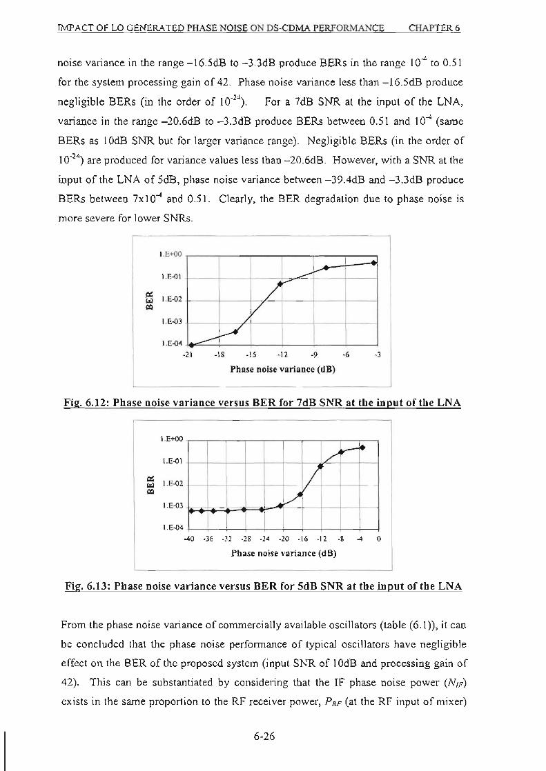
IMPACT OF LO GENERATED PHASE NOISE ON DS-CDMA PERFORMANCE CHAPTER 6
noise variance in the range - 16.5dB to - 3.3dB produce BERs in the range 10-4 to 0.51
for the system processing gain of 42. Phase noise variance less than - 16.5dB produce
negligible BERs (in the order of 10-24). For a 7dB SNR at the input of the LNA,
variance in the range - 20.6dB to - 3.3dB produce BERs between 0.51 and 10-4 (same
BERs as IOdB SNR but for larger variance range). Negligible BERs (in the order of
10.24) are produced for variance values less than - 20.6d.B . However, with a SNR at the
input of the LNA of 5dB, phase noise variance between - 39.4dB and - 3.3dB produce
BERs between 7xlO-4 and 0.51. Clearly. the BER degradation due to phase noise is
more severe for lower SNRs.
I .E+OO
I.E-O I
'" \ .&02 '" co /
V I.E·.()3
J .E-04 ~
-21 -lB -15 -12 -9 -3
Phase noise vari ance (dB)
Fig. 6.12: Phase noise variance versus BER for ' dB SNR at the input oftbe LNA
I.E+OO I ,
I.E-OI /' 0:
I.E-02 '" '" 1.&03
/ I 1/
I. E-04 I I I I -40 · ] 6 · ]2 ·28 ·24 ·20 · 16 ·12 -8 -4 0
Phase noise variance (dB)
Fig. 6.13: Phase noise variance versus BER for SdB SNR at tbe input of the LNA
From the phase noise variance of commerciaHy available oscillators (table (6.1 », it can
be concluded that the phase noise performance of typical oscillators have negligible
effect on the BER of the proposed system (input SNR of lOdB and processing gain of
42). This can be substantiated by considering that the IF phase noise power (NIF)
exists in the same proportion to the RF receiver power, PRF (at the RF input of mixer)
6-26
lMPACf OF LO GENERA TEO PHASE NOISE 0 OS-COMA PERFORMA CE CHAPTER 6
as the phase noise was to the oscillator power if it passes through no narrowband
filtering capable of limiting its bandwidth [72]. Expressed mathematically.
Nip I SNR I This relation was verified in the simulation. As an IF dB", = IlF dB .. - LO dB'
example consider, the existing setup with a - 80dBm signal power at the input of the
mixer and a typical LO SNR of 50dB (variance = -SOdB). The noise power additive to
the IF port using the above equation is - 13OdBm. However, computation of the noise
power (with the aid ofFriis ' equation [18]) in the absence of phase noise yielded an IF
noise power of - 91.35dBm. Thus the phase noise contribution of - 130dBm to this
noise power is negligible. The effect of phase noise has different degrees of impact
on the system's performance dependent on the PSK modulation type. This is intuitive
from the signal-space representation of various PSK formats. In [65] and [79]
expressions have been derived for the BER as a result of phase noise for both BPSK
and QPSK modulation. It has been mathematically shown that the phase noise
contribution to the BER for 7t/4 QPSK modulation is not severe even when the phase
noise performance is relatively poor. Thus it can be concluded that, in general, it is
unnecessary for oscillator specifications to be overly restrictive in terms of phase
noise. However, being overly restrictive with this phase noise specification, places
less demand on the low-noise design of other components in the RF system. Phase
noise can be minimized by careful design of the LO source. Phase noise in an
oscillator is proportional to the inverse square of its resonator Q, so considerable
improvement can be attained through the use of a cavity-or-dielectric-resonator
stabilized oscillator [70]. Crystal oscillators have low phase noise and are often used
with a multiplier chain to generate microwave LO signals. However. frequency
multiplication (which is in reality phase multiplication) enhances phase noise spectral
density a::; the square of the multiplication factor, so high-order multiplication of a
noisy source should be avoided since phase noise is worse in higher frequency
oscillators [72].
6-27

MIXER THEORY CHAPTER 7
CHAPTER 7
MIXER THEORY
7.1 Introduction
The mixing or frequency conversion process has been highly prevalent in the previous
chapters: Recall in chapter 3, the concept of an all-digital adaptive array is currently
impractical. This was solely due to the non-availabi lity of signal processing and
digitization hardware at typical communication frequencies. However. the use of a
mixer for frequency downconversion, has made digital adaptive beam forming
practically realizable. Although the mixer in this instance is an analog device, the
entire receiver chain is often perceived to be digital. It must be borne in mind that the
mixer is common to both analog and digital adaptive array receivers. The distinction
in these receivers is made in the implementation of the phase shifting and summing
circuits (chapter 3). Furthermore, some practical characteristics of mixers have been
encountered in the previous two chapters (chapters 5 and 6). This device was quoted
in chapter 5 as being the dominant source of noise in the receiver. Hence most of the
simulation results present there were focused around the mixer noise figure. Even
when considering the impact of LO phase noise in the DS-CDMA system of chapter 6,
the LO phase noise that leaked from the LO port to the IF port of the mixer was of
paramount concern (not the LO phase noise in isolation).
An overview on mixer theory is presented in this chapter. An understanding of some
of the properties of this ubiquitous device are warranted, especially in the
implementation of the BPSK RF front-end (chapter 9). For example, knowledge of the
concepts of sum and difference frequencies (generated by the mixing process) are
crucial for the selection of the appropriate LO frequency for a given RP and desired IF.
Also an understanding of intermodulation products also provide insight on the IF filter
requirements to filter unwanted inteffilodulation products. These become more
apparent in chapter 9. Amongst other issues covered in this chapter are the parasitic
signals (generated by the mixing process) and some principal characteristic of mixers
(e.g. conversion gain/loss, VSWR, noise figure, etc). lnterrnodulation products are
7-1
MIXER THEORY CHAPTER 7
demonstrated by a simple ADS simulation. This chapter ends with a discussion on
intermodulation distortion and design techniques to avert these unwanted responses.
7.2 Mixing or frequency changing
Mixing or frequency changing is a nonlinear operation that transfers the characteristics
of a signal of frequency fA to one of frequency Is. In most cases, this is done in order
to take advantage of the fact that the conditions for propagation are better at high
frequencies while the possibilities for signal processing are greater at low frequencies
and the costs are less. Also, at the lower frequency, the signal can be amplified and
demodulated most effectively. Mixers can also be used as phase detectors and in
demodulators, must perform these functions while adding minimal noise and
distortion.
When a sinusoidal signal is applied to a linear circuit, the output signal has the same
single frequency as the input. If the same signal is applied to a nonlinear circuit,
hannonics of the input frequency then appear at the output. When two sinusoidal
frequencies are applied to a nonlinear circuit, not only does the output signal contain
hannonics of both, but other frequencies appear that are not harmonics of either. The
concepts of mixing and frequency multiplication are essentially bound up with the
nonlinearity of the circuits involved and the amplitude of the input signaL A
convenient way of describing the transfer characteristic of a non linear device is the use
of a power series:
Where Vo = output voltage
Vi= input voltage
A,B,C,D, ... = constants
(7.1 )
When two sinusoidal signals VI and V1 with respective frequencies!1 andJi are applied
to such a nonlinear circuit, the expression for the output voltage contains many tenns.
By substituting
(7.2)
into equation (7.1), then:
7·2

MrXER THEORY CHAPTER 7
V. = A(V, + V, ) +B(V, + V, ) ' + qv, + V, )' + ....
= ~VL +BV]2 +CV]3 +K",V]"' } ~ V2 +BV/ +CV/ + K",V2"' } (7.3)
~B~V2 +3CV12 V2 +3CVI V/ + ... +KVl"' V/ ]
The first set of bracketed tenns represents the output voltage obtained when the signal
VI alone is applied to the nonlinear circuit: it can be shown by using trigonometrical
identities that the term in V /m generates the harmonic of frequency m/!. The same
reasoning can be applied to the second set of bracketed terms to show that the term in
Vzm generates the harmonic mlz from Vz. The third set of bracketed tenns is the sum of
cross products obtained from the expansion of the powers of (VI + V2). It can be
shown that the general term V,mVlll generates two frequencies, the sum and difference
frequencies, given by:
Sum frequencies: m[., + n/2
Difference frequencies: nz.f., -11/2 where m and 11 are integers.
(7.4)
(7.5)
A highly nonlinear transfer characteristic generates many frequencies if two sinusoidal
signals are applied. This is typical large-signal behavior: at the output there are two
original (amplified) sinusoidal frequencies, the hannonics of both and all the sum and
difference frequencies. The amplitudes decrease as m and 11 increase. The sum and
difference frequency signals are known as intennodulation products. The first two sets
of bracketed tenns in equation (7.3) produce hannonic distortion, while the third
produces intennodulation distortion. Note that an increase in these two types of
distortion amounts to a dispersal of power and thus a loss of power from the
fundamental frequencies.
A bandpass filter is used at the output of the mixer to allow only the desired frequency
to pass - generally that of the desired intennodulation product and in practice nonnally
the difference frequency (downconversion). The sum frequency is sometimes used for
upconversion in transmitters. In most case one of the signals (here V,) will be much
greater than the other to ensure large-s ignal behaviour i.e. a large excursion around the
operating point to obtain intennodulation products. The large signal is generally called
the LO (local oscillator) signal. Since the RF signal Vz often arrives from a receiving
7-3
MIXER THEORY CHAPTER 7
antenna, it is small; this is reinforced by the fact that for h the intennodulation
products of high index will have a very small amplitude.
A mixer also incorporates an input circuit to combine the RF and LO signals correctly
before applying them to the active nonlinear component. For this purpose, either a
directional coupler, a transfonner at relatively low frequencies or a hybrid coupler at
high frequencies is used to combine the signals and to isolate them from each other. If
conversion to a low or intennediate frequency is desired, the LO frequency [w is
usually tuned to a frequency above that of the received RF carrier and the difference
frequency signall!w - IRF) is selected while the other signals I!w,JRF and Ji.o + IRF) are
rejected by filtering [18]. The La frequency is almost always higher than the RF
carrier frequency, a characteristic referred to as the high-side injection of the mixer and
the system is referred to as a superheterodyne system.
7.3 Parasitic signals
A mixer generates many difference frequencies with values given by mJi - nj2. where
111 and 11 are integers. It is therefore possible for values of m and Il to occur that
produce frequency differences close to /1 - Ji. These undesirable signals are liable to
pass through the output bandpass filter, which must therefore have a narrow
bandwidth. In addition, the operating point and the excursion along the characteristic
CUlVe (i.e. the amplitude of the local oscillator) should be such that cross products of
order greater than 2 are negligible. Note that such parasitic frequencies are generated
for high values ofm and 11.
Another type of undesirable signal, this time at the input, consists of the image
frequency /;m. It is the second RF frequency that creates a response at the IF. For
example, if a mixer is designed to convert 8GHz to IGHz with a 7GHz LO, the mixer
will also convert 6GHz to IGHz using the same LO frequency. It is defined by:
ft. = 21,0 - I RF =2J, - I,
(7.6)
Thus a mixer can accept a signal of frequency /;m as an input signal. This is the reason
for all mixer circuits having an input filter to reject the image frequency. Consider the
following examples: If the local oscillator is at 2750MHz, input frequencies at
7·4
MIXER THEORY CHAPTER 7
2740MHz and 2760MHz will generate the same lOMHz output. Here the lower limit
of the input frequency range is lower than the LO frequency. In a conventional
receiver, where the lower limit of the IF output is higher than DC, this problem can be
solved by adding a RF filter to limit the input bandwidth. For example. if the input is
from 2750MHz to 3250MHz and the LO is at 1750MHz, the IF output is from
lOOOMHz to 1500MHz. The image entering the IF passband is from 250MHz to
750MHz in the RF input, which can be filtered out easily with a RF band pass filter
from 2750MHz to 3250MHz. !fthe LO frequency is at 2750MHz, with the same input
bandwidth from 2750MHz to 3250MHz, the IF output is from 0 to 500MHz. The
image is from 2250MHz to 2750MHz. This image (2250MHz to 2750MHz) will be
very difficult to filter out because the desired input (2750MHz to 3250MHz ) is
adjacent to it. A filter with a finite slope to pass the 2750MHz - 3250MHz frequency
range wi ll not effectively stop the signals in the 2250MHz - 2750MHz range.
The spurious output is another undesirable aspect that should be considered during
downconversion: A mixer used to downconvert an input signal to a proper IF range is
usually considered as a linear device, but strictly speaking, it is a nonlinear device. In
addition to the desired frequency, a mixer would produce many other frequencies,
often called the spurious output. The spurious frequencies can be determined using
equations (7.4) and (7.5) by
10 = ml, + Ill, (7.7)
where m and n are integers and /1 and /z are the input frequencies. Figure (7.1) shows
a mixer spur chart for the detennination of spurious responses. The desired output of a
downconverter is on the diagonally straight line marked H-L. H and L represent the
higher and lower frequencies of input signals /1 and /1. In a conventional
superheterodyne receiver design, where the IF bandwidth is narrow, the output is
chosen such that there are no low ordered spurs in the IF bandwidth, such as in the
region A of the spur chart. If an IF is from dc to a certain range. the spurs of 2H-2L.
3H-3L, ... are always included. For example. if the input is from 2750MHz to
3250MHz and the local oscillator is at 2750MHz, the output is from 0 to 500MHz
represented by square 8 where 6 spurs are included. Square B is obtained by use of
the following two equations:
7-5

MlXER THEORY
.£ or J, H f ,
H -L flF or-H f,
CHAPTER 7
(7.8)
(7.9)
The use of equations (7.8) and (7.9) yields values of 0.846 and 0.154, respectively. If
the input is from 750MHz to 1250MHz and the local oscillator is at 750MHz. the
output is from 0 to 500MHz represented by square C (equations (7.8) and (7.9) yields
values of 0.6 and 0.4, respectively). This square contains many more spurs than square
B. In general, the smaller the percentage bandwidth with respect to the local oscillator
frequency, the less spurs the output contains.
D.'
~'" M~! i~Jt., f\ . L-1 \
, fdi 11:
~
1\ \'- f\ '/ ,j rViI /1\ I) "\ V\A\ '/ !\hi
!j 11 ~ ,\ tIt.~ , C
7/ V " i\I M\\ fill y
If!/L/ \\ (IY~ ,,~t:;
V i . r. ... ,. 'J;J/, I";:
D.' , OD
MIXER SPUR CHART
Fig. 7. t: Mixer spur chart (from (30))
7-6

MIXER THEORY CHAPTER 7
7.4 Principal characteristics of mixers
7.4.1 Voltage standing wave ratio fYSWR) p
The VSWR gives a qualitative measure of the match for each of the mixer ports. It is
expressed mathematically as
(7 .1 0)
r = Z j -z ... (7.11) Zi + Z"
where Z; is the input impedance of the mixer at the frequency concerned (IF, LO, RF)
and Zc is the characteristic impedance (usually 50n). The VSWR is closely related to
LO amplitude which determines the operating point of the component. When the RF
level is ZOdB below the LO level. the VSWR that is used to calculate the filtering and
matching circuits, is taken as unchanged. The value of p is generally defined by the
manufacturer for a LO power having a value at the midpoint orits range of variation.
7.4.2 Isolation
The isolation is defined as the insertion loss between two tetminals of the mixer for a
given RF, LO or IF frequency. Its value is given by the manufacturer, over a range of
frequencies, as a function of the LO level and sometimes of temperature. The LO
inputIRF input and LO inputIIF output are the only ones quoted. The RF inputllF
output isolations is only given if the RF level is such that there is a risk of some RF
persisting at the IF output.
7.4.3 Dynamic range
This is the range of RF power over which it is possible to use the mIxer. The
minimum threshold is generally the nOIse, and the maximum limit is the IdB
compression point of the mixer.
7.4.4 The IdB compression point
A mixer has an almost constant conversion gain (defined in section (7.4.7» over the
whole of its dynamic range, which implies that when the RF signal increases, the IF
signal also increases. This only lasts until an RF level is reached at which PIF versus
PRF characteristic begins to show saturation. The saturated output level of a mixer is
7· 7

MIXER THEQRY CHAPTER 7
usually defined by its I dB compression point. The RF amplitude that produces an IF
level 1 dB below that corresponding to a linear extrapolation of the characteristic is
called the IdB RF compression point. Alternatively, the IdB compression point is the
output power point at which the conversion loss increases by 1 dB.
Beyond this point, intcrmodulation products of higher orders appear and there is a
transfer of power fromJiF to/= mfRF + n/w (with m;t;l and lI;;tl) , which is undesirable
from the user' s point of view. The value of the IdB compression point is related to the
amplitude of the LO signal.
7.4.5 The intermodulation intercept point and the corresponding powers
The intercept point I is defined as the point at which the output power In the
intennodulation products is equal to the IF output power, The input and output powers
P/i and Plo at the point I are related by
(7.12)
all in dBm. Gc is the mixer conversion gain. A high P/i guarantees a large dynamic
range and a good value for the 1 dB compression point. The manufacturer generally
gives the value of Pfj or P'o for intermodulation products of the third order (2/Lo - /RF, 2/RF - /Lo) or for double intermodulation products of the third order (with two RF
sources, one wanted, one parasitic):( ±2fRF/ ±fR" ±fw; ±fRFI ± 2fRFl ± fw). This is
warranted by the fact that the frequencies of the double products of the third order are
very close to JiF are not attenuated very much by normal mixers.
7.4.6 The noise factor, F
This is generally defined for a single sideband (SSB) system by the following
relationship:
F,,, (dB) = G, (dB) + IOIOg,,( IF lIoise power) RF nOise power
For a double sideband (DSB) system,
Fos. (dB) = F". (dB)-3dB
(7.13)
(7.14)
The difference between the RP and IF noise power is produced by the active and
passive components used in the mixer. The type of noise in question are I/ f (flicker)
noise from carrier generation and recombination, thermal noise and shot no ise. Mixers
7-8

MIXER THEORY CHAPTER 7
with high intermediate frequencies are affected only by white noise (thermal and shot)
and thus have better noise characteristics than those with low lFs which are subject to
l /f noise. This accounts for all the investigations being carried out with the aim of
reducing I/ fnoise level [69] for active components that can be used in low-lF mixers.
The noise factor of mixers is measured in the same way as for amplifiers, except that
the signal and noise power levels are compared at different frequencies (!iF and t RF).
From the point of view of noise, it is essential to reject the image frequency since, if a
signal of frequency f = /LO -/tF is the RF source for the mixer, the signal f = /La + /IF =
/;m is also converted to the frequency JiF. This doubles the amount of noise at the (f
output and thus increases the noise factor of the mixer.
7.4.7 Conversion gain G,
The conversion gain (or loss) of a mixer is defined mathematically as
G~ = 1010g1o
( IF power ) RF power
(7.15)
All mixers have a 3dB loss because one of the two sidebands is eliminated. The
conversion gain is always negative for a diode mixer (DM) and is on the whole
positive for a transistor mixer (TM). The value of Gc is closely related to the local
oscillator amplitude and the type of mixer [70].
A simulation using ADS software was perfonned to detennine mixer conversion gain
and the IF spectrum (intemlodulation products). The lAM81081 mixer by Avantek
was used. A RF frequency and power level of 2GHz and - 50dBrn, respectively was
used. For a desired (f of 68MHz, the LO frequency was selected (using equation
(7.5)) as 1932MHz. The LO level was chosen to be - 5dBm (within the specified LO
operating level of the lAM 8 I 081 mixer). Note that the LO level is much larger than
the RF signal level. As discussed in section (7.2) , this is to ensure large signal
behaviour to obtain intennodulation products. Figure (7.2) shows the ADS simulation
circuit schematic.
7-9

MIXER THEORY CHAPTER 7
SIMULATION or NOISE FIGURE AND CONVERSION GAIN RF = 2000 I.I H ~. 1 F = 68MHz. LO = 19J2MHz
•
-r '"
"()IOI,
'-' :050 0 .... HARMONIC BALANCE •
•• 4 .... ,· · (·· · ··_·~1 I' ... n ....
~" ,-, 1-'0 0.", .04" .. '.· 1_') <· ... lO'· ••
IiCi"l UW 'A!'I'
~ • • C'_.<. _~o _l1li .. "r, ••• _ ~ooc .... .
." 00.0 ..... )
.. • .. I'I·lClr' .q ~ , .. J """rI ll.
°"" 1' 1_' 0'4 .. 1 =, "pvl 'o •• or, •••
MV'" ""."_'" It 101''~O l ''- If' '.0 K .. . ...... ('1 ....... 1· ~u. "r ••• , .. o, .. , -o" '~ o , - ~o .. ' _"f
OPTIONS
0., '0"" ' ..... -1.-•• 1 ... ,0 .. '~ .. ~-••• ~-'lo lr.'.' ._1 ,-q. ".,.,.-. OI ••• " ... ,.I.u-...
LO, ... - l'll .... . ,r " ••• u" .. -lor •••
..o"".'. ,~ .,-'o
s;~rol'." conv.'lonc. '. mo', eo,; Iy q \lolnDC r \ft e 10r; e,1
I-I.Ill) -· . . ... ·q • • . i q no, (v,vOlly ,he lO) " r,cq[l].
It '. o.,,..,, , •• ,,,r. 1 0 vOl <."01> 1 •• G",n.~ ,n VAR b lod3 In mo."" ome.t oquotlon1. ~ rovl dod tt'1 c vOfio" ' C I Of . 01 , . , ;>tc<:I 01 OUIVOf . unO.r In. l i m"'ot ion eon"oll."
Fig. 7.2: ADS circuit schematic for simulation of mixer conversion 2ain and IF
spectrum
The conversIOn gam was determined by writing an expressIOn evaluating the
difference between the RF and [F power levels. The conversion gain was computed to
be 11.611dB (figure (7.3)).
I!IIConve r s i onGo i n==:dBm(H8. Vi f [1] ) - ( -50 )
Conv er$ionCoin
Fig. 7.3: Expression for determination of conversion gain
Figure (7.4) shows a plot of the IF spectrum. The relevant data is extracted and
conveniently disp layed in table (7. 1). It should be noted that the desired 68MHz IF
power level is above that of the - 50dBm RF level by that of the conversion gain
(11.61 I dB). The IF frequencies listed in table (7.1) are obtained by application orthe
sum and difference frequency equations (equations (7.4) and (7.5» for m + n ~ 5. To
speed up simulation time, the maximum order of the RF signal was set to 5. It should
be noted that the IF spectrum consists of all intermodulation products for m + n ~ 5. In
7-1 0
I
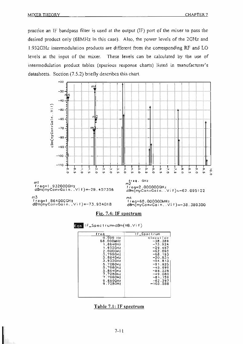
M IXER THEORY CHAPTER 7
practice an IF band pass filter is used at the output (IF) port of the mixer to pass the
desired product only (68MHz in this case). Also, the power levels of the 20Hz and
1.932GHz intermoduIation products are different from the corresponding RP and LO
levels at the input of the mixer. These levels can be calculated by the use of
intermodulation product tables (spurious response charts) listed in manufacturer's
datasheets. Section (7.5.2) briefly describes this chart.
- 20 ml
-JO
• -"
> -50
< "
I I I I -BO
0 ~ > -70 < J
-I 0 u ~ -BO ~
E m ~ - 00
-'00 - 110
I ~-I , • 00_ N N ~ ~ ~ • ~ ~ ~ ~ ~
o ~ 0 ~ 0 ~ 0 ~ 0 ~ 0 ~ 0 ~ 0 -..I 00 00 ...
U'I 0 U'> 0 . " ml f' e,/=1 .932000GHz d8m myConvGoin .. Vi f)=-29.457306
m3 f ,e,/=, .864000GHz dBm myConvGo in .. Vi f )=-73.924018
freq. CHz m2 f ,e,/""'2. OOOOOOGH z dB"n myConvGa in .. Vi f )::-62.095122
m+ f,e,/=68.000000MHZ dBm myCo nvGa in .. V if) =-38.389300
Fig. 7.4: IF spectrum
l1li t F _Spec t r I.ST"I="d8m( HB. V i f)
f" It_Spectrum 0.000 Ht
68.000MHz 1.864GHZ 1.932GHz 2 . 000GHz ,J.796GHz ,J.854GHz ,J.932GHz .!).728GHz 5.796GHz '!).86~GHz 7. n8GHz 7.796GHz "9 . 660GHz 9.728GHz
Tab le 7.1: IF spectrum
7-11
..;:inva l id:> -38.389 -73.924 -29.457 -62.09.5 -58.193 -20.931 - .54.813 -91.62.5 -4.5.699 -as .228 -49.080 -81.759 -62.297
- 103.588
MIXER THEQRY CHAPTER 7
7.S LO-Induced noise, intermodulation and spurious signals
The sensitivity of a microwave receiver is usually limited by its internally generated
noise. However, other phenomena sometimes affect the performance of a mixer front
end more severely than noise. These are AM noise (amplitude noise). phase noise,
spurious signals and intennodulation products. AM noise and phase noise have been
thoroughly discussed in the previous chapter (chapter 6). The discussion here is
limited to intennodulation distortion and spurious responses.
7.5.1 Two-tone intermodulation and saturation 1701
Mixers are subject to gain saturation and two-tone intennodulation. Mixer operation
requires that the RF input level be kept well below the LO level. As the RF level
approaches the LO level, there is gain saturation and distortion. The saturated output
level of a mixer is usually defined by its I dB compression point, the output power at
which its conversion gain decreases by IdB. For the same LO level, active FET
mixers have higher IdB compression points than diode mixers. Increasing the output
level of a mixer requires increasing its LO drive.
Diode mixers have high levels of multitone IM (intennodulation). IM is manifest as
the creation of distortion products when two closely spaced RF input tones (e.g. at
frequenciesJi and!1) generates other tones at the frequencies
f", = ±qf, ± rf, ± sf La (7. 16)
where q, r, S are positive integers.
The worst of these are the third order (q + r = 3) products at 2fi • f, and 2f, - fi
downconverted to the iF. These distortion products are generated by the
nonlinearities in the solid-state device used to perfonn the mixing. The large-signal
LO, in addition to the small-signal excitations, convert the intennodulation products to
the IF frequency and to sidebands of all the LO hannonics.
The spectrum of intennodulation products in a mixer is shown in figure (7.5).
7·1 2

MIXER T H ERR Y CHAPTER 7
S(ij
l1ro
tI1 t dt t1! t • 12 -I, 21,-12 1, 12 212 - 1, 21, L 21"2 ~'~ ~, f
12 + " 212 ", " 21, .. 12
Fig. 7.S: Spectrum of the interrnodulation products resultine: from two RF inputs
(from 170])
The intermodulation products up to thi rd order are shown. These are "folded" around
each LO harmonic. [n the lower curve of figure (7.S),J, andJi are IF frequencies. As
long as the mixer is not saturated by the RF tones. the levels of IM at the IF port
depends on the levels of the excitation. A graph showing linear output levels and IM
levels versus input levels is shown in figure (7.6).
10
o
P..." , dBm -10
INTERcePT POINT
UNEAA OUTPUT LEVEL
,
././// ..... i
!
lM OUTPUT LEVEL
Fi2. 7.6: The third-order intercept point (from 170()
The third-order intercept point is the extrapolated point where the IM levels and linear
output levels meet. By convention P in and P out are the output levels of each tone. The
level of intennodulation products at the output of the mixer is given by the well
known relation [81]:
Pm = np' - (n-l)JPII •
(7.17)
7-13

MIXER THEORY CHAPTER 7
where 11 is the order of the lM product, IPn is the 11th-order intercept point of the IM
product in question, and P J is the output level of the linear responses, assumed to be
equal. All power levels in equation (7.17) are in dBm. Note that IP,) is the
extrapolated point, in terms of output power, at which the input-output curves of the
linear and IM responses intersect.
Equation (7.17) shows that the levels of the 11th-order IM product vary Il dB for 1 dB
change in input level of both input tones. Closer inspection of the analysis leading to
equation (7.17) would show that the 11th order IM product given by equat ion (7.16).
where q + r = 11, varies q dB for every IdB change in ji. and r dB for every IdB
change in ji. This principle, in combination with the intercept point and equation
(7.17), can be used to find the IM level that results from any set of input levels.
When a mlxer IS cascaded with either RF preamplifiers or an IF amplifier, the
calculation of intercept point for the cascade is complex. The intercept point for each
stage is amplified or attenuated by the next stage, along with the desired signal, and
new IM products are generated. These new IM products occur at the same frequency
as those of the previous stage but their phase is indetenninate. Thus, the IM products
may combine in such a way as to either enhance or reduce their magnitude. This
process is repeated at each subsequent stage. An upperbound on the intercept point
can be detennined by assuming that the IM products generated in each stage, and
those passed along from previous stages, add precisely in phase. This is a reasonable,
worst-case assumption. Under this assumption. the worst-case output intercept point
ofa cascade of stages ([811. [821. [83]) is:
IPft
(1 - ,.)/ 2 = IP~.}I ft) / 2 + (G m IP".", _l 11-
10)/ 2 + (G ",G m- JP.. ,m-2 YI-,,)/2 +
.. , + (G2 ... GmfP~'1 ) 1-,,)12 (7.18)
where 11 is the order of the IM product, m is the number of stages, and subscripts refer
to the stage numbers.
In any receiver, the mixer is the dominant source of intennodulation distortion. Its
contribution can be minimized by using minimal gain in the low-noise RP amplifiers
preceding it. Minimizing the noise temperature of the receiver, however, requires the
use of substantial amplifier gain. These are conflicting tradeoffs, which are resolved
7-14

MIXER THEORY CHAPTER 7
only by using no more gam ahead of the mixer than is necessary to meet nOise
temperature goals. The better the mixer design, the less low-noise amplification is
needed. and both noise temperature and intermodulation level will benefit.
Minimizing preamplifier gain also improves spurious-response levels by reducing the
input level at the mixer.
7.5.2 Spurious responses
Spurious responses are a type of single-tone intennodulation. The frequencies of
spurious responses are given by equation (7.16) when either q = 0 or r = O. However,
unlike conventional multi tone intennodulation, in a spurious response, a harmonic of
the LO other than the one that causes the desi red frequency translation often figures
prominently. As mentioned earlier, the mixer generates output frequencies that satisfy
the relation
(7.19)
where m, n "'" 0, ± I, ±2, ... and/IF'/RF and/ware the IF, RF and LO frequencies,
respectively. This equation is similar to the sum and difference frequency equations
of (7.4) and (7.S). Thus there exists a wide range of frequencies, many of which are
outside the RF passband, whereby interfering signals can be converted to the IF.
If the input frequencies satisfying equation (7.19) are well outside the input passband,
the interfering signals can be removed easily by filtering. If the spurious response is
of a high order (i.e. high values of m and 11), the mixer would not convert them
efficiently to the IF. The problem becomes serious when the RF frequencies of low
order spurious responses are within the mixer's input passband, or are so close to it
that they cannot be filtered effectively. The best way to avoid spurious responses is to
select RF, LO and IF frequency ranges appropriately. An understanding of spurious
responses can be gained through the following example. Although the frequency
range from this example is different from that used in the project, the knowledge
attained is useful. Figure (7.7) shows a spurious-response plot and table (7.2) shows a
level chart for a 29GHz to 30GHz mixer having a 3GHz to 4GHz IF passband.
7-15

MIXER THEORY
40 -
,----------_______ (m,n)
_ 1·'.3) 35 -
IF RF PASSBANo-, PASSBAND
30 ~1'4 -- I I- I I
T _ (2, -2)
(3, ·3)
'5 I- (·3,3)
I I I ~_I 1.1,1) I I·',') 20 , 3 5 6 7
CHAPTER 7
Fig. 7.7: Spurious response plot for a 30GHz mixer (LO freguencv = 26GHz)
(from 1701l
Since none of these curves intersect the shaded area, this mixer has no in-band
spunous responses.
Sporious·lh:Sponsc l.cvcls or;1 2'). 10 J()· ( jlll. MhI:cr )( inl.liQlcs Ih::.1 nos-pu r ex ists within the 2(1 . to 4(}'Glb. RI' r.IOGC
10 IIflrnlmlic (n):
RI: fi llmwnic (/11):
IF Fn:qu..:ncy:.1 104 Gl u. In FM!\lcrn:y: 26 GJ b:
1.0 I.evel: t 13 dlJm RFI..cv£I:-l0dBm
,J , 3 -70 • 2 • - 45
• • - 1 • • -2 • • -} • •
, • • • • -46
•
J
• • • • -M
-70
Table 7.2: Spurious-response levels of a 29GHz to 30GHz mixer (from [70])
The plot in figure (7.7) is simply a piot of equation (7.19) for several low-order
combinations of m and 11 . Spurious responses (including the image, which can be
treated as the low-order spurious response (m ,lI) = (-1 , 1» are plotted over the range
7-16

MIXER THEQRY CHAPTER 7
of input fTequencies from 200Hz to 40GHz and IF frequencies from zero to 80Hz.
Note that the defined RF and IF ranges have been exceeded, because spurious
responses outside the defined passband may still be a source of trouble. The response
of greatest concern in this example is the (2. -2) response from 27.5GHz to 28GHz,
close to the lower edge of the passband, because it has relatively low order. It is close
enough to the RF passband that it may be difficult to eliminate by means of a filter.
The spurious-response chart, table (7.2), shows the spurious-response levels of the
mixer. The response levels in the chart were measured with the LO level set at the
mixer's standard value, in this case 13dBm, and at an RF input level of - 1 OdBm (this
input level has become an infonnal standard for specifying spurious~response levels).
The chart includes the effects of filtering and matching circuits that may be used in the
mixer. In some cases, the input frequencies that give rise to a particular spurious
response cannot be measured ~ thus there is no entry in the table for this. For other
types of mixers, such as a broadband balanced mixer, the table would be nearly full.
The ~ I OdBm level is a compromise: it is not high enough to cause saturation. so the
data in the table can be scaled to different input levels, yet it is still high enough to
allow accurate detennination of some fairly high-order (and therefore weak)
responses. These data can be scaled to different RF input levels [82] by recognizing
that spurious responses are a type of intermodulation. Like other intennodulation
products, the response associated with the mth hannonic of the RF input changes m
dB for each dB change in RF input level. Thus, a reduction in RF level of IOdS
reduces the (2, -2) response by 20dB, or the (-2,3) by 30dB. This principle can be
used to determine the amount of filtering needed to reduce any spurious response to an
acceptable level. Note that this principle does not apply to the LO level, or to RF
levels strong enough to saturate the mixer.
One of the fundamental uses of LNAs ahead of a mixer is to minimize a receiver's
noise temperature. This has been established in chapter 5. Because of the way mth
order spurious responses and intennodulation products vary with input level. the use
of an LNA can seriously degrade the receiver's intennodulation and spurious-response
perfonnance. For example, suppose an LNA having 20dB gain is added to the input
of a receiver having a mixer front-end. The extra 20dB of signal level at the input of
7-17
MIXER THEORY CHAPTER 7
the mixer will increase the level of a (2,11) spurious-response by 40dB. and will
degrade the carrier-to IM level by 20dB; a (3,/1) response will be degraded (in tenns of
carrier-to-IM ratio) by 40dB.
7.6 Conclusion
Some important issues and properties of mixers were highlighted in this chapter. An
understanding of simple concepts such as the generation of sum and difference
frequencies (that are often taken for granted), enable selection of the appropriate LO
frequency for a given RF and desired W. The issue of the LO drive level always being
specified larger than the RF drive level in manufacturer's datasheets also become
apparent. Also, as discussed, the mixing process generates, in addition to the desired
IF, other unwanted intermodulation products. These unwanted products are removed
by an IF bandpass filter. Thus, it is not uncommon to find these IF bandpass filters in
RF front-ends. This is also evident in the implementation of the BPSK RF front-end
(chapter 9). These characteristics where taken into consideration in the
implementation of the RF front-end of chapter 9.
Other issues, though not related to this project, not only are of interest to the reader,
but also provides insight into this ever-present device.
7-18

LOW NOISE AMPLIFIER DESIGN CHAPTERS
CHAPTER 8
LOW NOISE AMPLIFIER DESIGN
8.1 M otivation
This chapter presents the design, simulation, construction and characterization of a
low noise amplifier (LNA) intended for use in the BPSK RF front-end system
(chapter 9). The LNA specifications of interest (noise figure and gain) are crucial to
this investigation. With knowledge of these specifications for each of the front-end
blocks, the overall noise figure (using Friis' equation) can be computed. Thus the
SNR and the Error Vector Magnitude (EVM) degradation of the system can be
measured. Hence the LNA can be specified for a given SNR or EYM system
requirement.
Due to the initial expected delay in the arrival of the commercially available LNA
(ZEL· I724LN) used in the BPSK system, the need for the design and construction of
an in-house LNA was further motivated. However, it was not possible to characterize
the noise fi gure of this LNA at the frequency of interest (2GHz). The reasons for this
have been outlined in section (8.6.1). As a result, the delay cost incurred in the arrival
of the commercial product was accepted, and the ZEL-1724LN was included in the
BPSK RF front-end (figure (9.1)). Nevertheless. a Jaw-cost, in-house solution, with
the possibility of demonstrating acceptable system performance, is an attractive and
viable option.
8.2 Introduction
In wireless communication systems, a fundamental function of the RF front-end
section is signal amplification. In the case of a receiver, the lowest possible signal
level at its input must be amplified to a level that can be detected by the demodulator.
I.n the transmitting case, the transmitted signal must be amplified sufficiently so that
8-1
LOW NOISE AMPLIFIER DESIGN CHAPTER 8
despite losses inherent in wireless transmission, the signal can be received by the base
station.
There are several types of amplifiers that serve specific functions in the RF front-end
of the communication system. In the receiv ing chain, amplifiers that are closest to the
antenna contribute directly to the noise performance. As established in chapter 5,
these LNAs must have a low noise figure and provide adequate gain so that noise
contributions from the remaining of the receiving components are negligible. in the
transmit path, the amplifiers closest to the antenna are power amplifiers (PAs). They
must amplify the signal linearly and efficiently [65]. However, noise is not a primary
consideration in PAs. Chapter 5 also made brief mention of the near-far effect which
is eliminated by power control. In this instance, the receiver incorporates automatic
gain control (AGe) in either the RF LNA or IF amplifier. The function of these
v~riabl e gain amplifiers (VGAs) is to help keep the receiver output constant over the
expected range of signal level. The noise and linearity speci fications/requirements of
VGAs are not stringent as that for LNAs and PAs, respectively. However, the
dynamic range of VGAs must be reasonable i.e. it must be able to handle both the
levels of small and large signals.
The basic topology of microwave amplifier ci rcuit des ign is straightforward. Often
the only components involved are an active device (transistor or FET) plus four or
fi ve microstrip transmission line elements of various lengths and widths. Compared
to a large analog I.e. chip or a digital microprocessor chip. such a microwave circuit
seems very simple. However, the design of microwave amplifiers poses many
technical challenges to electronic circuit designers.
High-frequency amplifier design has traditionally followed the route of an art rather
than a science. Engineers would carry out approximate calculations and then make
the amplifier circuit work by means of tuning, shielding, grounding and the design of
a good layout. However, in addition to the above techniques, scattering parameters
are today used in microwave amplifier des ign work because they arc easier to measure
and work with at high frequencies than are other kinds of parameters. They are
8-2

LOW NOISE AMPUFrER DESIGN CHAPTER 8
conceptually simple, analytically convenient, and capable of providing insight into a
design problem.
The approach followed in the designing of a practical high-frequency amplifier is
based on the following six steps:
I. Define a specification
U. Select an active device
IT!. Select a topology
rv. Select a bias circuit
V. Perform a computer simulation and optimization of the circuit to realize the
specification.
Vl. Construct and lest to verify that the design meets the specification.
VI], Adjust simulation to achieve measured results (Steps V to VTI are perfonned
iteratively).
The necessary tools for the design of microwave amplifiers are found from an
understanding of transmission lines, two port networks and impedance matching
networks. With the knowledge and understanding of scattering parameters, the design
of amplifier circuits is essentially an impedance matching problem. Ln order to
understand this design, it is assumed that the reader is familiar with basic network
analysis and the elementary concepts of microwave amplifier design theory. A
detailed theoretical analysis of microwave amplifier design can be found in [63], [84],
[85], [86], [87] and [88].
The first step in the design process is the definition of the specifications. It is intended
to use to this amplifier in the proposed COMA adaptive array system. The
specifications have been appropriately defined as:
• Centre frequency of 2GHz
• Required operating power gain 2: lOdB
• Minimum 3dB bandwidth of IOMHz (This bandwidth is commensurate with the
4.096MHz chip rate of WCDMA. A bandwidth of 8.192MHz (2 x chip rate) is
required for BPSK modulation)
8·3
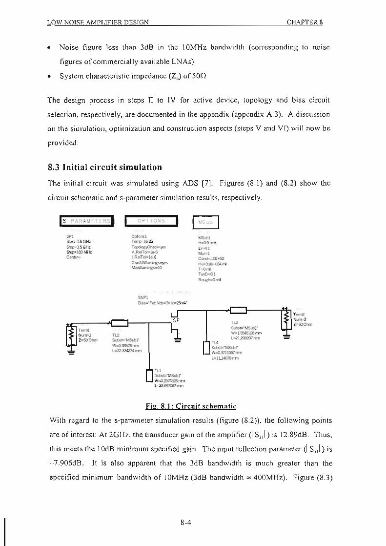
LOW NO ISE AMPLIFIER DESIGN CHAPTER 8
• Noise figure less than 3dB in the IOMHz bandwidth (corresponding to nOise
figures of commercially available LNAs)
• System characteristic impedance (Zo) of son
The design process in steps U to IV for active device, topology and bias circuit
selection, respectively, are documented in the appendix (appendix A.3). A discussion
011 the s imulat ion, optimi~atiun and construction aspects (steps V and VI) will now be
provided.
8.3 Initial circuit simulatio n
The initial circuit was simulated using ADS [7}. Figures (8.1) and (8.2) show the
circuit schematic and s-parameter simulation results, respectively.
Is PARAM[T ERS ' I OPT ONS I
'" StIrtoJ.5Gi'il Silp=3.5 Gi'il Step.< lOOMHz c_
=
Op'onsl Terrpol6.85 T(IJXIk;iB.,checlF)e$ V_RelToI=Ie-6 LRelToI"le-6 G...eAIWMl'l:!S=)eS MalW;nqs=1O
... , H..o9mn E,=41 ..... , ConcI=I.CE+50 Ho.3.~rril
TeOml TrO.:I.1 Rqh=Oml
m Stbs""'MSWI" W= I 554512>mn L=21_2:Q2/J7 mn
Fig. 8.1: C ircuit schematic
With regard to the s-parameter simulation results (figure (8.2)), the fo llowing points
are of interest: At 2GHz, the transducer gain of the amplifier (1 52]1) is 12.89dB. Thus,
this meets the 10dB minimum specified gain. The input reflection parameter d Sill ) is
- 7.906dB. It is also apparent that the 3dB bandwidth is much greater than the
specified minimum bandwidth of I OMHz (3dB bandwidth ~ 400MHz). Figure (S.3)
8-4

LOW NO ISE AMPLIFIER DESIGN CHAPTER S
shows the noise figure verSllS frequency simulation results. Once again it is apparent
that the noise fi gure is less than 3dB within an approximate bandwidth of 1.25GHz.
The simulation results indicate that the amplifier meets all the specifications.
However, the large value of the input reflection parameter (-7.906dB) is a cause for
concern. The input reflection parameter (I Sill ) is a measure of the quality of the input
match. It is the ratio of reflected power to transmitted input power at port 1 of the
device. It is thus desirable to make this parameter as small as possible. The next
section focuses on optimization of the circuit fo r an improved input match.
" .. , • I-
=~~ N _ N_ • • •• 10 NN __
~~~ ,. ."." ." ."
" • • /
• ..
6.0 \
,., '.0
., • ' .0 E ~
z ,.,
'.0
2.'
2.0
1.5 , ..
"-"- /
/
" , ,
" " " n n .. , , , , " " " "
, t .. q. CHz
Fig. 8.2: S-paramcter simulation results
\ /
\ V \ V
'" V r-.. V
" .. , 2.0 2.2 2.' 26 2.' '0
freq, GHz
Fig. 8.3: Noise figure versus freguencv
8-5
"
/
m' , .. q:2.000GHz dB{S(2. 1»)=12.890
m2 , .. q:2.000GHz d8($(2. 2»)=·S.904
m' freq:2.000GHz dB($( I .I»)=·7.906
m • , req:2 .000GHz B(S (l. 2»)z·23.056 0
"
/

LOW NOISE AMPLIFIER DESIGN CHAPTER 8
8.4 Optimization
8.4.1 Fundamentals of optimization
Often in the design of a microwave amplifier, the initial responses - gain. noise figure,
input or output VSWR, and so on - do not exactly match the specified values over the
frequency band of interest for many reasons. For example. the model may not exactly
represent the measured data; other causes of error include the unilateral assumption in
the case of transistors. or the distributed approximation of the lumped elements.
[n order to obtain the specified response. the elements of the original network can be
adjusted by the cut-and-try method (tuning); this usually limits a network to a few
elements and a narrowband response. For a large broadband network, this type of
tuning is a tremendous and often impossible task. Therefore it is more appropriate to
adjust the response of the initial network by varying its elements iteratively according
to some numerical algorithm carried on a digital computer. This process is called
optimization. Since optimization is an iterative process, the procedure is laborious,
and for a broadband ampli fi er the number of iterations cou ld easily be a few hundred
even with the most efficient currently available optimization methods - if the response
of the initial network deviates too far from the specified one. Furthermore, the
optimization process may fail or may converge to an inferior network with poor
starting values.
8.4.2 Optimization of input matching network
The simulation results in section (8.3) indicate that the amplifier meets all the
specifications. As mentioned, the large va lue of the input reflection parameter
(-7.906d.B) is a cause for concern. This can be attributed, inter alia, to the non
consideration of the biasing lines, step-width change discontinuity [89], coupling and
bypass capacitors in the simulation model. There is thus a need to optimize the circuit
for an improved input match or lower input reflection parameter (1 SIll ).
Tuning is one of the simplest optimization tools in ADS. In this instance, the length
of the quarter-wave transfonner (between 50n input line and input open circuit stub)
was tuned/opt imized for an improved input match. An optimum value of - 26. 765dB
8-6

LOW NOISE AMPLIFIER DESIGN CHAPTERS
for the input reOection parameter cl Sill) was obtained for a 13.867mm transmission
line length. Thus, a reduction in the length of the quarter-wave section from
22.334mm to 13.867111m resulted in a reduct ion in 1 s,,1 from - 7.906dB to - 26.765dB.
Figures (8.4) and (8.5) shows the optimized s-parameter simulation resu lts and noise
figure versus frequency plot, respectively.
" " , , •
dB ,
." ~
~
.»
• •
• . ..:
•
•• • ~ ,
• , ,
• ,
-t--l
,.,.",. ,.uuuuu _u uuuuuuuu u
'-I.G'h
Fig. 8.4: Optimized s-parameter simulation results
\ I I
J I1 I
\ / I \ V I
/ I """ V I
I
m' IreQ: 2.000GHz NFmin=1 .655
.. , .. .. " " ••• " " " .. .. freq. GH~
Fig. 8.S: Noise figure versus frequency (after optimization)
On comparison of the oplimized simulation results of fi gures (8 .4) and (8.5) with that
of the initial circuit (figures (S.2) and (S.3)), optimization also resulted in a marginal
improvement in gain cl S211) from 12.89dB to 13.793dB and a decrease in the noise
figure from I.S5SdB to 1.655dB. It is evident that the 3dB bandwidth is greater than
8-7
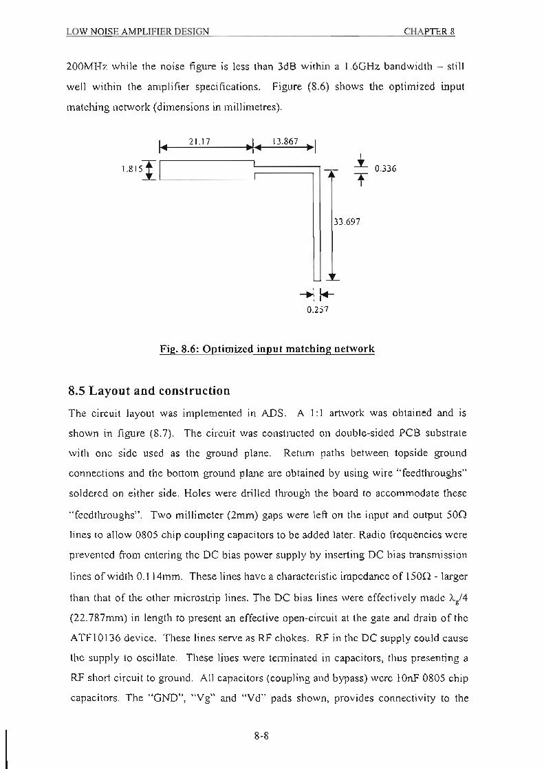
LOW NOISE AMPLIFIER DES IGN CHAPTER S
200MHz while the noise figure is less than 3dB within a J.6GHz bandwidth - still
well within the amplifier specifications. Figure (8.6) shows the optimized input
matching network (dimensions in mil limetres).
I ~ 21.17 13.S67 . 1
I.S151 L====~====ll 1.. T
33.697
--.Jf4-0.257
Fig. 8.6: Optimized input matching network
S.5 Layout and construction
0.336
The circuit layout was implemented in ADS. A I : 1 artwork was obtained and is
shown in fi gure (8.7). The circuit was constructed on double-sided pes substrate
with one side used as the ground plane. Retum paths between topside ground
connections and the bottom ground plane are obtained by using wire "feedthroughs"
soldered on either side. Holes were drilled through the board to accommodate these
"feedthroughs". Two millimeter (2mm) gaps were left on the input and output 50n
lines to allow 0805 chip coupling capacitors to be added later. Radio frequencies were
prevented from entering the DC bias power supply by inserting DC bias transmission
lines of width 0. 114mm. These lines have a characteristic impedance of 150n -larger
than that of the other microstrip lines. The DC bias lines were effect ively made ')../ 4
(22.787mm) in length to present an effective open-circuit at the gate and drain of the
ATFlO l 36 device. These lines serve as RF chokes. RP in the DC supply could cause
the supply to osci llate. These lines were tenninated in capacitors, thus presenting a
RF short circuit to ground. All capacitors (coupling and bypass) were 10nF 0805 chip
capacitors. The "GND", "Vg" and "Vd" pads shown, provides connectivity to the
8-8

LOw NOISE AMPLIFIER DESIGN CHAPTER 8
ground, gale and drain inputs, respectively of the power supply (see figure (A.Il) in
appendix A.3). Figure (S.S) shows a picture of the complete amplifier.
Footprints for IOnF ~ bypas~ (decoupling) ~ •• ~ capacitors V •
ATFI0136GaAs device
'i V" 150n DC bias lines
Pads for the source leads of the ATFIOl36 GaAs device (these pads are connected via "feedthroughs" to the underside ground plane)
sits here
;:-~~~~-/ 1 ~IF'll OI ITF'lf T , 50n input son output
~ ~ Footprints for IOnF coupling capacitors
Fig. S.7: Circuit artwork (1:1)
Fig. 8.8: Complete amplifier
S-9
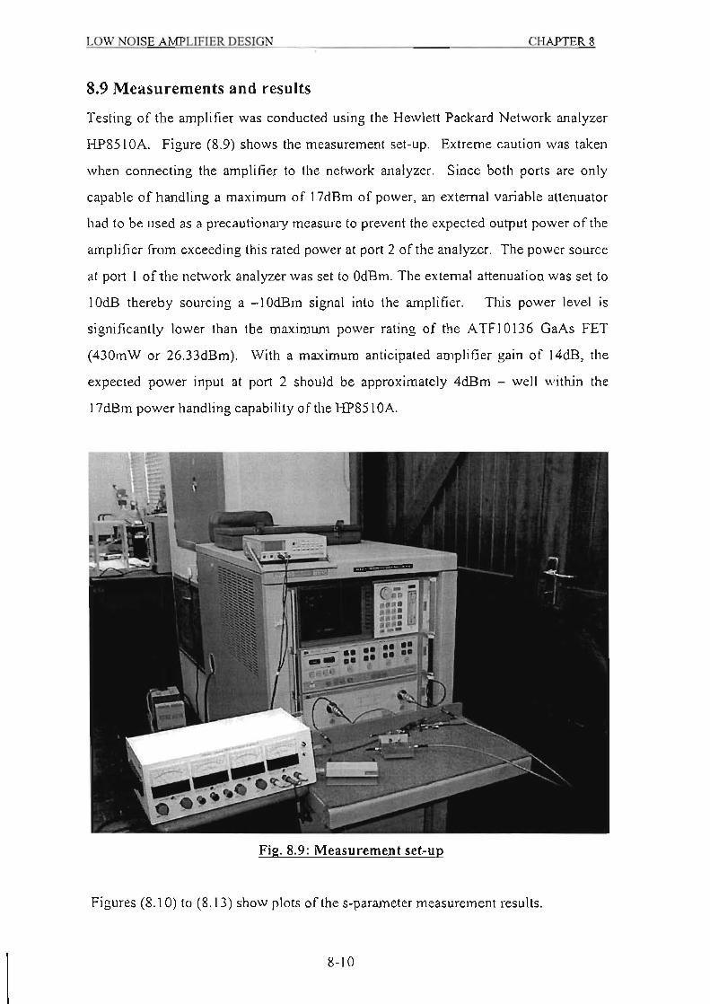
LOW NOISE AMPLIFIER DESIGN CHAPTERS
8.9 Measurements and results
Testing of the amplifier was conducted using the Hewlett Packard Network analyzer
HP8510A. Figure (8.9) shows the measurement set-up. Extreme caution was taken
when connecting the amplifier to the network analyzer. Since both ports are only
capable of handling a maximum of 17dBm of power, an external variable attenuator
had to be used as a precautionary measure to prevent the expected output power of the
amplifier from exceeding this rated power at port 2 of the analyzer. The power source
at port 1 of the network analyzer was set to OdBm. The external attenuation was set to
IOdB thereby saUTeing a - lOdBm signal into the amplifier. This power level is
significantly lower than the maximum power rating of the ATFlO136 GaAs FET
(430mW or 26.33dBm). With a maximum anticipated amplifier gain of 14dB, the
expected power input at port 2 should be approximately 4dBm - well within the
17dBm power handling capability of the HP85l OA.
Fig. 8.9: Measurement set-up
Figures (8.1 0) to (8.13) show plots of the s-paramcter measurement results.
8· 10

LOW NOISE AMPLlFIER DESIGN
... S11 Icg ~
c
1
REF" 0.0 cS .£ 10 . 0 c:EV V -1:5 a77 cS . '" MAR~ER
2.111 C Hz PO'" 11O~
I
I • I
,
1 I .1 , -"
f\ v V
-
STMT 1 .~GHz STOP :3. fZI0ZIIZIi:'001Z11Z1 CiHz
. '-1 I I I I I , I i , I I I I I i i I I I
1 I I
I i I j
Fig, 8,10: S-parameter measured result I silL
~ 10,10 oS Ica MAO
~ 10.0 c:£V 13.071 c:I3
'" I I , c MAR~ER C
,111 'Hz po . 1""
~ !--I
. I 1 I --
"- V I ,
I -... \/ I I ! I
V I i 1I I i ,- +-1_; ~ I
! J START 1.~ Gtz. STOP 3.12XNJ0211211Z11 Gtz:
Fig. 8.11: S-parameter measured result 1 s!lL
8·11
CHA PTER 8
1.B GHz · -10 . a~ t:I3
""'""<ER 2 2.0 GHz -1S.B?? dE
""'""<ER 3 2.c Gb!:: -? . 63"" dE
Ea Al.JCj 001 la.19:~6
1.8 G-Iz:.1. 14.392 cE
~2 2.0 GHz
13 . lOn dE
~3
2.2 GHz dE 9.5C78

LOW NOISE AMPLIFIER DESIGN
c
1
~ " ... dl log '""'"
~ 121 . III c::e.---23.121:5:5 c13
'" 1 1 I 2 I
, MAR1ER ,
.IZ! Hz , FXHn .~.
1 I I 1 I ,-H "1
I I I I I I , I I ~ I ,
! '~ , , v.., / I
'\ / I I START 1 .1ZI00J2'II2WZ" Gb:: STOP 3.~GHz
Fig. 8.12: S-parameter measured result I s.l
~~ .. ... dl .& 112t. 0 c:£V V -S.EA77 cI3
log ~
I
C ~R ER ~~!---f----~--+---~---r---+--~ 2.1Z! GHz I
I -1
1
- --1-'-+-- - '
r---l--'! i L..-...L-..--'....i _ LI_"---'--_.L11 ---,. __ L __ I_l
STFfIT 1.~ CiH:: STOP 3. 02ICZII2I0IZI00 GI-Iz
Fig. 8.13: S-parameter measured result I s,zL
8·12
CHAPTERS
1.B (lHz'
-aa . 768 C£
2 2 . " GHz c£ -23 . 05S
~:3 2.2 GHz c£ -25.183
I .28 A.JG 0211 18: 12:Z6 .
1..8 G-tz 1.
-2.829 c£I
""""""" 2 2 . 0 GHz -5 ...... 77 C£
""""""" :3 2.2 Gtz -11.271 c£
28 AUG 01Z1\ 18:17:32

LOW OISE AMPLIFIER DESIGN CHAPTERS
Table (8.1) compares the measured s-parameter results with that of the simulation
(after optimization) at the 20Hz centre frequency.
S-parameters Simulation results (after
optimization) Measured results
I s,,1 -26.8dB -IS.9dB
I s,,1 13 .8dB 13.1dB
I s,,1 -22.2dB -23. 1dB
Is,,1 -3.9dB -S.6dB
. . Table S.l: Comparison of simulated and measured s-parameter results
As can be seen in table (8.1), there is good correlation between measured and
simulated s-parameter results, with the exception of the input reflection parameter
(I Si ll ). Nevertheless, an input reflection parameter of - 15.9dB is reasonable.
The gain of the device was measured to be 13.1 dB. The 3dB bandwidth was
computed as 520MHz (Q factor of 3.85) which exceeded the minimum specified
IOMHz bandwidth. A broadband design has thus been achieved.
8.6.1 Noise figure measurements
Procedures and techniques for noise figure measurements are described in [91], [92]
and [93J. The technique described in [91], utilizing a spectrum analyzer, has been
deemed the best measurement choice for the following reasons:
a) The noise figure can be measured at any frequency within a spectrum analyzer's
frequency range. This enables measurement at the device's operating frequency
without changes in the test set-up.
b) Due to the frequency selectivity of spectnIm analyzers, noise figure measurements
are independent of device bandwidth or spurious responses.
However, as with any other measurement, the analyzer's sensitivity and accuracy
become limiting factors in noise figure measurements. The technique outlined in [91]
has a limitation: the noise output of the device under test (DUT) must be greater than
8-13

LOW NOISE AMPLIFIER DESIGN CHAPTERS
the analyzer's internal noise level so that it can be measured. If the noise output of the
OUT is below the analyzer's sensitivity level, its power must be raised by a low-noise.
high-gain preamplifier. Then the noise level measured by the spectrum analyzer is
greater than the device's output noise by the preamp' s gain.
Due to inadequate gain of the designed amplifier and the inavailability of a preamp at
the desired frequency, this technique (utilizing a spectrum analyzer) could not be
used. lnstead, another straightforward technique utilizing a HP346B noise source and
HP8970B noise figure meter.
The basis of noise figure measurements using a noise source and noise figure meter
depends on the noise linearity characteristic of linear two-port devices. The nOise
power out of a device is linearly dependent on the input noise power or nOlse
temperature (Ts) as shown in figure (8.14). No is the noise power added by the OUT.
p
Power output (W)
Slope - kG.B P ""'PU'
N,
~--::-----=-_T. o Source temperature (K)
Fig. 8.14: Noise linearity cbaracteristic of a linear two-port device
I f the slope of this characteristic and a reference point is known, the output power
corresponding to a noiseless input power, Na can be found. From Na, the noise figure
F can be calculated using the well-known relation,
F = N. +kT. BG kT. BG
This equation appeared in chapter S.
8- 14
(8.1 )

LOW NOISE AMPLIF IER DESIGN CHAPTERS
From figure (8.14), for a source impedance with a temperature of absolute zero, the
power output consists solely of added noise Na from the OUT. For other source
temperatures the power output is increased by thermal noise from the source amplified
by the gain of the OUT. The noise slope is determined by applying two different
levels of input noise and measuring the output power change. A noise source is used
(0 provide these two known levels of noise.
The HP346B noise source consists of a low-capacitance diode that generates noise
when reversed biased into avalanche breakdown with a constant current [941. When
the diode is biased, the output noise will be greater than kTeB (thermal noise) due to
avalanche noise generation in the diode. When unbiased, the output will be the
thennal noise (kTeB) produced in the attenuator of the noise source. These levels are
called Th and Te corresponding to the tenns "hot" and "cold" .
The HP346B produces nOIse levels approximately equal to IOOOOK when on and
290K when off. To make noise figure measurements a noise source must have a
calibrated output noise. The excess noise ratio (ENR), expressed in dB is the ratio of
the difference between Th and Tc. divided by 290K,
EN 0 1 ~T',-:-:-,T-,-, • RdB = I og-
T. (8.2)
It should be noted that a OdB ENR noise source produces a 290K temperature change
between its on and off states. 11 is often erroneously believed that the ENR is the "on"
noise relative to kTB. However, this is not the case.
Te in equation (8.2) is assumed to be 290K when it is calibrated. Noise sources are
supplied with an ENR tab le giving the ENR versus frequency values. The noise fi gure
meter uses ENR and the Y-factor method as the basis of noise figure measurements.
Using a noise source, this method allows the detennination of the internal noise in the
OUT and thus the noise figure. With a noise source connected to the DUT, the output
power can be measured corresponding to the noise source 0 11 (N2) and the noise
source off (N 1). The ratios of these two powers is called the Y-factor,
8- 15

LOW NOISE AMPLIFIER DESIGN CHAPTERS
y = o utput power with noise source on = N 2
output power with noise source off N1 (S.3)
or in dB units, Y' B = 10 log Y .
The V-factor and ENR can be used to find the noise slope of the DUT that is depicted
in figure (8.14). Since the calibrated ENR of the noise source represents a reference
level for input noise, an equation for the internal noise (Na) of the OUT can be
derived. In a noise figure meter, this is automatically detennined by modulating the
noise source between the on and off states and applying internal calculat ions,
N ~ kT nG( ENR -I ) a " Y-l
(S.4)
From this an expression for the noise figure can be derived. The noise figure that
results is the total system noise figure, Fsys- It includes the noise contribution of all
the individual parts of the system. In thi s case the noise generated in the noise figure
meter has been included as a second stage contribution. If the gain of the OUT is
large, the noise contribution from this second stage will be negligible. By subst ituting
equal ion (S.4) into equation (S.l),
(S.5)
When the noise figure is much higher than the ENR, the device noise tends to mask
the noise source output. In this case the Y-factor will be very close to I. It is difficult
to measure small ratios of the Y-factor accurately. For this reason, the Y-factor
method is generally not used when the noise figure is more than IOdB above the ENR
of the noise source, depending on the measurement instmment.
Table (8.2) shows the noise figure results fo r the designed amplifier at three
frequencies. These results were obtained using the HP346B noise source and
HP8970B noise figure meter. Measurements were restricted to a frequency of 1.8GHz
which is the maximum operating frequency of the noise figure meter. At 1.8GHz the
simulated noise figure (after optimization) from fi gure (8.5) was 2.2dB while the
noise figure measurement yielded 2.7dB. At 1.7GHz and 1.75GHz, noise figures of
3.2dB and 4.97dB respectively, were measured. Simu lated noise figures (after
8-16

LOW NOISE AMPLlFrER DESIGN CHAPTER S
optimization) of 2.8dB and 2.5dB at l.70Hz and l.75GHz, respectively were
obtained. Unfortunately, no correlation/comparison between simulated and measured
noise figure (at the desired frequency of2GHz) could be made.
Frequency Noise figure
1700MHz 3.2dB
I 750MHz 4.97dB
1800MHz 2.7dB .
T able 8.2 : NOise figure measurements uSlDg the HP346B nOise source and
H P8970B noise figure meter
8.7 Conclusion
It was the intention of the author to specify, design and construct an LNA with
parameters that would provide acceptable performance of the HPSK RF front-end of
chapter 9. However, due to the reasons cited in section (8.6.1), the noise figure of the
LNA could not be measured. Nevertheless, a low-cost, in-house 2GHz broadband
low-noise amplifier (with 13.ldB gain and 520MHz 3dB bandwidth), for possible use
in the adaptive CDMA system, was developed.
Relevant theory focusi ng on amplifier stabi li ty was presented and a suitable design
technique, discussed and implemented. The topology of a low-noise high-frequency
amplifier seems very simple. Tuning, shielding, proper grounding techniques and the
design of a good layout plays an important role in the design of a fully functional
amplifier. To conclude, a firm theoretical and practical basis on microwave low-noise
amplifier design has been laid down in this chapter.
8- 17

MEASUREMENTS CHAPTER 9
CHAPTER 9
MEASUREMENTS
9.1 Objectives
The intention of this chapter is to verify and support the theory and simulation results
of the preceding chapters. The effect of RF component noise on OS-COMA system
performance was evaluated in chapter 5. Essentially, RF component noise (as a result
of the noise figure) causes degradation of the signal-ta-noise ratio (SNR) and hence an
increase in the bit error rate (BER). Thus it is intended to replicate the SNRs within
the measurement setup and compare the performance degradation between simulated
and measured results. In the previous chapters. the BER was used as a figure of merit
to quantify system performance. However, this chapter introduces a different
measurement method, the Error Vector Magnitude (EVM), which has been gaining
rapid acceptance in the wireless communication industry. In addition to providing a
figure of merit for system performance, it introduces a methodology for
troubleshooting possible impaimlents sources within a transceiver system that could
cause signal degradation.
The phase noise theory in chapter 6 is reinforced by phase noise measurements. This
section does not include all possible phase noise measuring schemes nor does it
examine any single method in detail. Attention here is given to the more sensitive
methods of phase noise measurement. Two such methods are the delay line method
and the phase detector method. Using the HP89410A vector signal analyser in
conjunction with the theory developed in chapter 6, a quantitative phase noise
comparison of two frequency sources is performed.
9-1
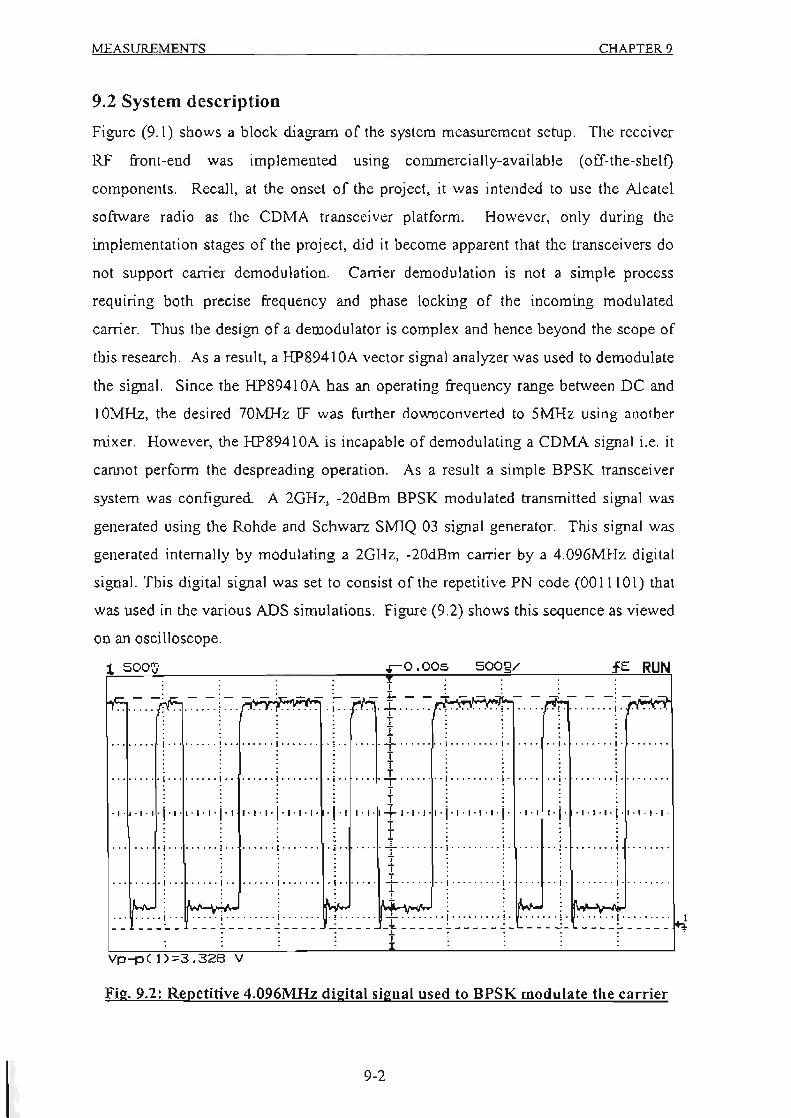
MEASUREMENTS CHAPTER 9
9.2 System description
Figure (9. 1) shows a block diagram of the system measurement setup. The receiver
RF front-end was implemented using commercially-available (off-the-shelf)
components. Recall , at the onset of the project, it was intended to use the Alcatel
software radio as the CDMA transceiver platform. However, only during the
implementation stages of the project, did it become apparent that the transceivers do
not support carrier demodulation. Carrier demodulation is not a simple process
requiring both precise frequency and phase locking of the incoming modulated
carrier. Thus the design of a demodulator is complex and hence beyond the scope of
this research. As a result, a HP8941 OA vector signal analyzer was used to demodulate
the signal. Since the HP8941 0A has an operating frequency range between DC and
lOMHz, the desired 70MHz IF was further downconverted to 5MHz using another
mixer. However, the HP89410A is incapable of demodulating a CDMA signal i.e. it
cannot perfonn the despreading operation. As a result a simple BPSK transceiver
system was configured. A 2GHz, -20dBm BPSK modulated transmitted signal was
generated using the Rohde and Schwan SMIQ 03 signal generator. This signal was
generated internally by modulating a 2GHz. -20dBm carrier by a 4.096MHz digital
signal. This digital signal was set to consist of the repetitive PN code (0011101) that
was used in the various ADS simulations. Figure (9.2) shows this sequence as viewed
on an osci lloscope.
500V .o .oo~ 500~/ f E RUN
••..•••.• ! ......... ! .. .. r· .... · .. r·
.... ! ........ ! .. '1" ..;.
r·i·
Vp -p( 1) 3.328 V
Fig. 9.2: Repetitive 4.096MHz digital signal used to BPSK modulate the carrier
9-2
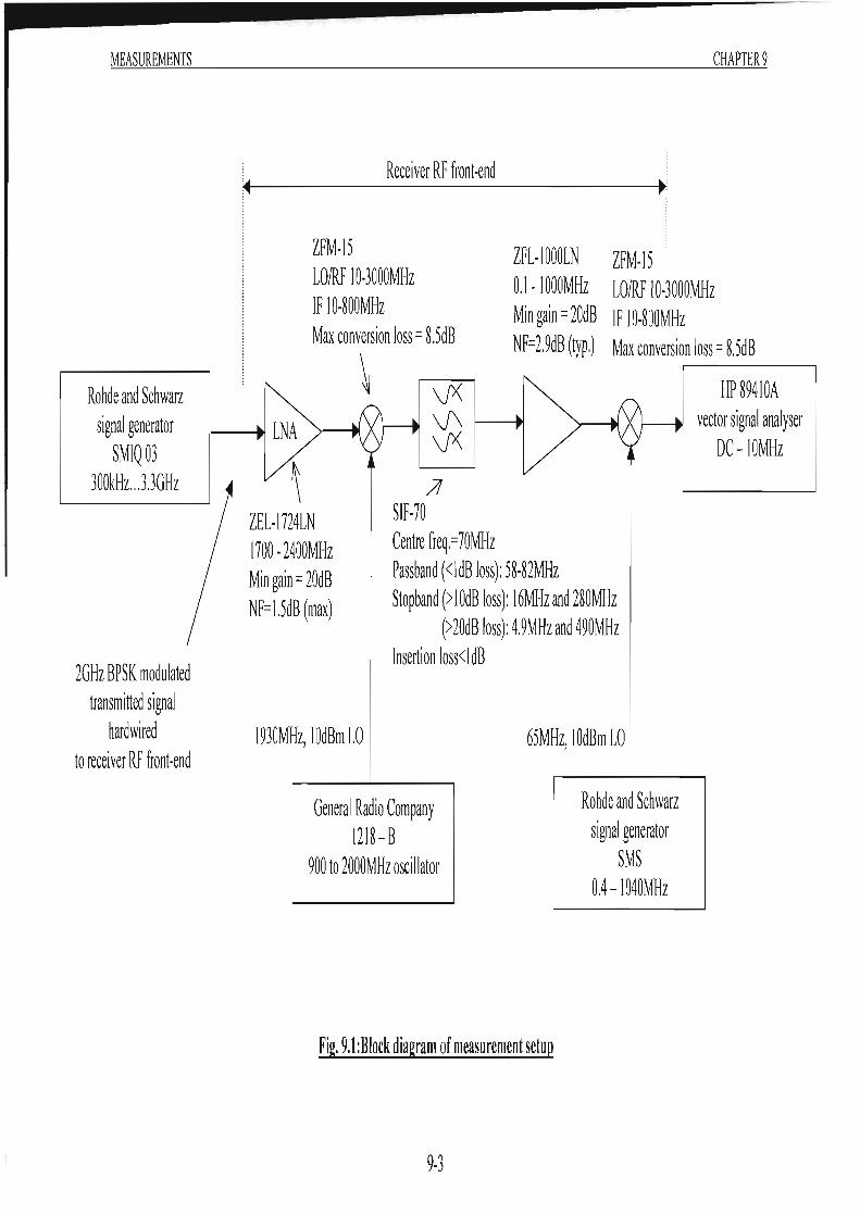
MEASUREMENTS
Rohde and Schwarz signal generator
SMIQ 03 300kHz ... 3.3GHz
2GHz BPSK modulated transmitted signal
hardwired to receiver RP front-end
CHAPTER 9
Receiver RF front -end
ZFM-l) ZFL-IOOOLN ZFM-l) LOIRF 10-3000MHz IF 10-~00MHz
O.l · lOOOMHz LOIRF 10-3000MHz Min gain = 20dB IF 1 O-~OOMHz
Max conversion loss = ~jdB
\ NF=2.9dB (typ.) Max conversion loss = ~jdB
1--- LNA , ZEL-I724LN 1700 -2400MHz Min gain = 20dB NF= 1 jdB (max)
1930MHz, 10dBm LO
)!
SIF-70 Centre freq.=70MHz Passband «ldB loss): )8·82MHz Stopband (> 1 OdB loss): 16MHz and 2~OMHz
(>20dB loss): 4.9MHz and 490MHz Insertion loss< 1 dB
6)MHz, 10dBm LO
General Radio Company 121~ -B
Rohde and Schwarz signal generator
SMS 900 to 2000MHz oscillator 0.4 - 1040MHz
Fig. 9.1:Block diagram of measurement setup
9-3
HP ~941OA vector signal analyser
DC - IOMHz

MEASUREMENTS CHAPTER 9
The 2GHz, -20dBm BPSK spectrum (for different frequency spans are shown in
figures (9.3) and (9.4).
MKR 2 . 000 0 GHz
Ip REFr-~~~~,--"~rc~~~ __ '-____ r-__ -' ____ -r-~3~·~·~·~·C~d~B~m, 1121 dS/
CEN TE R 2 . 0 00 GHz RES S W 100 kHz VSW 300 kHz
SPAN 400 MHz SWP 120 .... Q c
Fi2. 9.3: 2GHz, -20dBm BPSK modulated spectrum (400MHz span) measured at
output of Rohde and Schwarz SMIQ 03 signal generator
REFr-~.~.~.~d~B=cm-, __ ~A~T_T~E~Nc-l~.~d~B __ -r ____ -r ____ -r ____ -r ____ -r ____ , 1121 dS/
CENTER 2.121121121 121 GHz RES 8W 1121121 kHz vew 31210 kH z
SPAN 10.0 MH,z SWP 2121. ca meac
Fig. 9.4: 2GHz, -20dBm BPSK modulated spectrum (I0MHz span) measured at
output of Rohde and Schwarz SMIQ 03 signal generator
9-4
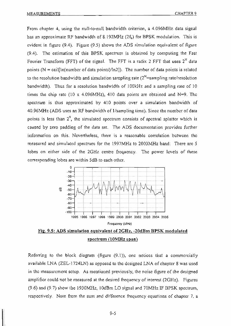
MEASUREMENTS CHAPTER 9
From chapter 4, using the null-ta-null bandwidth criterion, a 4.Q96MHz data signal
has an approximate RF bandwidth of 8. I 92MHz (2f.) for BPSK modulation. This is
evident in figure (9.4). Figure (9.5) shows the ADS simulation equivalent of figure
(9.4). The estimation of this BPSK spectrum is obtained by computing the Fast
Fourier Transfonn (FIT) of the signal. The FFT is a radix 2 FIT that uses 2N data
points (N ~ ceil[ln(number of data points)/ln2]). The number of data points is related
to the resolution bandwidth and simulation sampling rate (2N=sampling rate/resolution
bandwidth). Thus for a resolution bandwidth of 100kHz and a sampling rate of 10
times the chip rate (10 x 4.096MHz), 410 data points are obtained and N~9. The
spectrum is thus approximated by 410 points over a simulation bandwidth of
40.96MHz (ADS uses an RF bandwidth of l /sampling time). Since the number of data
points is less than 29, the simulated spectrum consists of spectral splatter which is
caused by zero padding of the data set. The ADS documentation provides further
infonnation on this. Nevertheless, there is a reasonable correlation between the
measured and simulated spectrum for the 1997MHz to 2003MHz band: There are 5
lobes on either side of the 2GHz centre frequency. The power levels of these
corresponding lobes are within 5dB to each other.
o ·10 ·20 ·30
·40
·50
·60
·70 ·80 ·90
-100+-,--,--,- ,--,--,--,--,-- ,---' 1995 1996 1997 1998 1999 2000 2001 2002 2003 2004 2005
Frequency (MHz)
Fig. 9.5: ADS simulation equivalent of 2GAz, -20dBm BPSK modulated
spectrum (lOMHz span)
Referring to the block diagram (figure (9.1», one notices that a commercially
available LNA (ZEL- I724LN) as opposed to the designed LNA of chapter 8 was used
in the measurement setup. As mentioned previously, the noise figure of the designed
amplifier could not be measured at the desired frequency of interest (2GHz). Figures
(9.6) and (9.7) show the 1930MHz, 10dBm LO signal and 70MHz IF BPSK spectrum,
respectively. Note from the sum and difference frequency equations of chapter 7, a
9·5

MEASUREMENTS CHAPTER 9
LO frequency of 2070MHz could also be used to generate the 70MHz IF. However,
the maximum operating frequency of the LO generator used here is 2GHz. The LO
signal power was set to 10dBm, commensurate with the specified LO drive level of
the ZFM-15 mixer. The ADS simulation equivalent of the measured 70MHz IF
BPSK spectrum (figure (9.7» is shown in figure (4.17) (chapter 4). On comparison of
figure (4.17) with that of figure (9.7), it should be noted that the spectra have a similar
appearance. However, the power levels of the spectra differ. The simulat ion model
used in chapter 4 did not consider component gains and noise figures. Furthermore,
the spread data was used to BPSK modulate a IOdBm 2GHz RF carrier (as opposed to
the - 20dBm RF carrier in this measurement setup). The simulation model in chapter
4 was merely intended to demonstrate CDMA concepts. MKR 1.930:3 GHz
Ip REFr-~2~0~.~0~d=B=m~~'~T~T~E=N~3=0~d=B~-' ____ -r ____ '-____ ~.='~?~0=r=.B~m-, 10 dB/
CENTER RES sw 100 kHz; V8W 300 kH:z SWP 30." malic
Fig. 9.6: 1 930MBz, lOdBm LO signal measured at output of General Radio
Company 1218·B oscillator
9·6
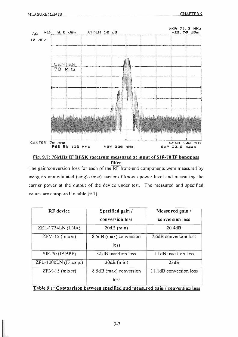
MEASUREMENTS CHAPTER 9
MKR 71. 3 MHz
Jp 'E~~_~~~~'-r~~~~.!'~0~~ __ ' _' __ '_'r_' ___ -'r ____ -;- 22.70 dBm
ll2l dB/
C;:'NTER 70 101H z RES 8W lee kHz vew 31210 kH%
----r -' --
SPAN 11210 MHz SWP 3121 . 121 maliC
Fig. 9.7: 70MHz IF BPSK spectrum measured at input of SIF-70 IF bandpass filter
The gain/conversion loss for each of the RF front-end components were measured by
using an unmodulated (single-tone) carrier of known power level and measuring the
carrier power at the output of the device under test. The measured and specified
values are compared in table (9.1).
RF device Specified gain I Measured gain I
conversion loss conversion loss
ZEL-1 724LN (LNA) 20dB (min) 20AdB
ZfM-IS (mixer) 8.5dB (max) conversion 7.6dB conversion loss
loss
SIF-70 (IF BPF) < ldB insertion loss 1.1 dB insertion loss
ZFL-1000LN (IF amp.) 20dB (min) 23dB
ZfM-IS (mixer) 8.SdB (max) conversion 11.1dB conversion loss
loss . . . Table 9.1 : Comparison between specified and measured gam I conversIOn loss
9-7

MEASUREMENTS CHAPTER 9
The overall gain of the front-end is computed as 23.6dB. Using the specified noise
figure for each component and the measured gain, the approximate overall noise
figure using Friis' equation [18]. [61]. [63] is computed to be 1.873dB.
9.3 Phase noise measurement
The most convenient way to measure phase noise is to use a common phase noise test
system. Such a system usually contains a state-of-the-art frequency synthesizer, a low
frequency spectrum analyzer and some dedicated hardware. Often, a second DSP
based spectrum analyzer is included to speed up and extend measurements close to the
carrier by using a Fast Fourier Transfonn (FFT) technique. The whole system is then
controlled by a computer with proprietary software. With these systems, it is possible
to determine phase noise levels both very close to and very far from the carrier.
As mentioned in chapter 6, the sidebands of a LO signal may represent both AM and
PM noise. Asymmetry in the side bands indicates that both AM and PM noise are
present. However, in many cases, the PM sidebands are dominant. For example, if a
reasonably clean synthesized signal is multip lied up to be used as a high frequency
reference, the phase noise sidebands are multiplied by the same factor as the
frequency while the AM sidebands are unchanged or are limited. In this case. direct
RF spectrum measurements at the multiplied frequency are a good approximation of
the phase noise sidebands. The sidebands, when corrected and nonnal ized to the
carrier powers, represent the L(j) spectral density described in chapter 6. One way to
achieve better resolution is to translate the signal down in frequency to the range of an
analyzer with the desired IF bandwidth. Figure (9.8) shows a typical setup using a
doubly-balanced mixer and a low pass filter. AM noise on the LO signal is rejected
by a balanced mixer. Also all (m,n) spurious responses (chapter 7) where m, n or both
are even are rejected by doubly balanced mixers.
Low pass filter I-----fo
Fig. 9.8: Sidcband translation
9-8

MEASUREMENTS CHAPTER 9
One of the advantages of this technique is that AM sidebands on the measured signal
will be stripped off if it is to be used as the high level signal at the mixer. However,
there are two potential problems:
a) The difference frequency will contain sidebands which are folded up from below
zero frequency. Whether or not the sidebands are significant depends on the
nature of the particular source being measured.
b) The phase noise sidebands from the reference frequency at the mixer will also be
translated down. This problem is avoided by using a source with better phase
noise specifications than the onc being tested.
Two requirements must be met in a phase-noise measuring scheme to reach a noise
floor low enough for the best oscillators:
a) The carrier's phase noise must be separated from its AM components.
b) Carrier must be el iminated. It must somehow be cancelled to measure its close-in
phase noise sidebands. A frequency discriminator is used to do this. Infonnation
on this is contained in [95].
9.3. I Delay line method
Figure (9.9) illustrates this method where the above two requirements are satisfied
Oscillator under test
Delay line
Low noise video
amplifier Selective Power splitter Mixer lA""" voltmeter
"-----~--.I t/ Amplitude adjust
Phase adjust
orFFT
Fig. 9.9: Delav line phase noise test equipment block diagram
The signal to be measured is divided into two equal parts. One-half goes through a
delay line, producing a quadrature phase shift of the carrier. The other-half,
undelayed except for an incremental adjustment is mixed with the delayed signal in a
homodyne detector. This cancels the carrier. The quadrature shift places one carrier
9·9

MEASUREMENTS CHAPTER 9
in phase with the other's quadrature or phase noise sidebands, as the mixing signal.
The demodulated signal is amplified for measurement. This scheme is insensitive to
AM noise. This technique does not require an extremely stable test oscillator, but it
has limitations imposed by the delay line requirements:
a) A long delay line means a low instrument noise fl oor
b) A long line also implies high transmission losses, so it must be driven by a power
amplifier to give the detector a minimum signal leveL This amplifier contributes
its own phase noise and converts signal amplitude noise to phase noise. If no
amplification is used, optimum de lay requires that the product of its length and
attenuation be unity. The product of its delay and offset frequency must be less
than unity. This latter condition limits measurements close to the carrier, as the
delay must be high to measure small offset frequencies.
The delay line may be made of any form of microwave transmission line. Coaxial
and waveguide lines are the most common. A coaxial air line gives minimum loss but
it is large. The waveguide line has the advantage that its group velocity is less than
that of light and decreases as frequency approaches cut-off. Attenuation also
increases at the same time. It is an optimum delay line but is bulky. A transmission
form of resonant cavity also may be used as a delay line. It has a much greater delay
per unit volume than a transmission line. However, it and the oscillator under test
must be quite stable. because the cavity must be tuned accurately to the oscillation
frequency.
9.3.2 Phase detector method
A phase detector scheme can be used to cancel the carrier and give quadrature mixing.
Figure (9.10) shows an elementary circuit for the phase detector method.
Oscillator under test
Locking Oscillator
DC amplifier
Lowpass filter
Locking signal
1-_-'--_-+ to Wave analyzer
Fig. 9.10: Block diaeram of the phase detector phase noise measuring system
9-1 0

MEASUREMENTS CHAPTER 9
The test and locking oscillators must be on the same frequency. and the locking
oscillator's phase noise must be either very low or a known quantity. The two
oscillator's signals are mixed, their difference frequency amplified, filtered and used
for phase lock. At offset frequencies above the locked bandwidth, the noise is the
sum of the two oscillator's phase no ise powers. This setup requires very stable free
running oscillators. The difference frequency must remain within a few hundred hertz
of the locking frequency for a short time (up to a minute or so).
9.3.3 Phase noise measurement and comparison of 2 frequency sources
The HP89410A vector signal analyzer was used to measure and compare the phase
noise performance of the Rohde and Schwarz SMIQ 03 and SMS frequency sources
(figure (9.1». The HP8941 0A has a phase noise measurement utility that eliminates
external hardware or circuitry (described above) thereby simplifying the measurement
process considerably. However, measurements are restricted to a carrier freq uency of
IOMHz (within the operating frequency range of the instrument). The setup simply
requires direct connection of the frequency source to the HP89410A. The instrument
then perfomls phase demodulation to eliminate the carrier thereby allowing the phase
noise to be measured. The power level and frequency of both sources was set to
IOdBm and 5MBz respectively. Figures (9.1 1) and (9.12) show the power spectral
density of phase fluctuations of both frequency sources for a resolution bandwidth and
frequency span of 300Hz and 20kHz, respectively. Note from chapter 6, the power
spectral density of phase fluctuations, denoted as SIJ) (= (JRMi), is expressed in units
of decibels below I rad' in a bandwidth of I Hz. Tables (9.2) and (9.3) show the single
sideband (SSB) level versus offset frequencies. Also shown are the single sideband
noise-to-signal ratio or variance (0-/) computed by use of equation (6.49) in chapter
6. The SSB levels in tables (9.2) and (9.3) have been extrapolated from figures (9.11)
and (9. 12) respectively. From the variance values of both frequency sources, it can be
concluded that the Rohde and Schwarz SMIQ 03 signal generator has considerably
better spectral puri ty or phase noise performance than that of the SMS signal
generator. This was anticipated at the onset of the measurement since the SMIQ 03 is
a much more recent model than the SMS.
9-11

MEASUREMENTS
TRACE A: Ch i PM PSD A M k w- er
-30 dB'
LogMu9
10 d
I d i B v
-13 dB
0 •
Y' = r adr I1s"'2/
00 . St art . 50 Hz
CHAPTER 9
- . 10 000 Hz 103 736 dB' z
'-
~ ..... ~
-.......
k I . Stop, 10 kHz
Fig. 9.11: Phase noise spectral density profile of the Rohde and Schwarz SMS
O.4MHz l040MHz signal generator (fo=5MHz, resolution baodwidth=300Hz.
frequency span-20kHz) -
Offset frequency SSB level (dBcIHz) variance (0/)
50Hz ·61
100Hz -59 -40.5dB
1kHz -82
10kHz -104
Table 9.2 : Phase nOise parameters of the Rohde and Schwarz SMS O.4MHz
1040MHz signal e.enerator
9- 12

MEASUREMENTS
TRRCE R: ChI PM PSO FI Markt2:r
-75 y> = radrl'ls"2/ dB>
LogMag
5 dB
Idiv
-125 dB> 00 . Start. 50 Hz
z
CHAPTER 9
- . 10 000 Hz 115 03B dB>
" 1"\
t--.. '-
" -k 1
Stop: 10 kHz
Fh!. 9.12: Phase noise spectral densitv profile of the Rohde aDd Schwarz SMIQ
03 300kHz 3.3GHz sienal generator (f.- 5MHz, resolution bandwidth-300Hz,
frequency span=20kHz)
Offset frequency SSB level (dBc!Hz) variance (cl)
50Hz ·89.6
100Hz -89.5 -66.4dB
1kHz -108
10kHz -114 . . Table 9.3: Phase nOise parameters of the Rohde and Schwarz SMIQ 03 300kHz
3.3GHz signal2.enerator
The resolution bandwidth and frequency span of the measurement instrument are
crucial to accurate phase noise measurements. Both these parameters are inter
related. The smaller the reso lution bandwidth, the greater the measurement accuracy
and the larger the instrument sweep time. For the HP8941 OA vector signal analyser,
the lower and upper bounds on the resolution bandwidth (RBW) are given by:
9-13

MEASUREMENTS
RBW . = ENBW x [span] mm (nun! of freq. pts.)-l
RBW=, =O.3x [span]
where ENBW = normalized equivalent noise bandwidth
span = frequency span
CHAPTER 9
(9.1)
(9.2)
IIllm offreq. pIS = number of frequency points required to interpolate the plots
To measure phase noise at a large offset frequency requires a corresponding increase
in both the frequency span and resolution bandwidth. This case is demonstrated in
figure (9. 13) where it is desired to measure the SSB level at an offset frequency of
20kHz. Table (9.4) shows the extrapolated data corresponding to some of the offset
frequencies (100Hz, 1kHz and 10kHz) of table (9.3). The SSB levels at offset
frequencies of 100Hz and 1 kHz do not correlate reasonably. This is due to the
interpolation of the spectrum as a result of an increase in frequency span and hence
the resolution bandwidth.
TRA CE A: Chl PM PSD A Marke:r
-9 8 dB>
LogMa9
2 dB
I di v
- t t 8 dB>
y> = radrl'ls"'21
tOO . Start. 100 Hz
z - . 20 000 Hz 1 t3 963 dB>
1\ '\ '\ ~ ~
~
k Ok St o p: 20 kHz
Fie:. 9.13: Phase noise spectral densitv profile of the Rohde and Schwarz SMIQ
03 300kHz - 3.3GHz signal generator (fo=SMHz, resolution bandwidth= lkHz,
freguencv span=40kHz)
9-14

MEASUREMENTS CHAPTER 9
Offset frequency SSB level (dBclHz)
100Hz -99
1kHz -105
10kHz -114
20kHz -114
-Table 9.4: Phase nOise parameters of the Rohde and Schwarz SM1Q 03 300kHz-
3.3GHz signal generator for resolution bandwidth of 1kHz and 40kHz frequency
9.4 Error Vector Magnitude (EVM) measurements
A fundamental function of the HP89410A vector signal analyzer, apart from carrier
demodulation, is to perform error vector magnitude (EVM) measurements. Thus far,
the bit error rate (BER) was used as a figure of merit for system performance. Poor
quality transmission can be seen as low or poor signal quality which may result in a
high BER. BER testers count the number of errors which cross certain
limits/thresholds. These instruments do not indicate why or how far out of limit the
signal is, or even if the error occurred in the transmitter or receiver. However, EVM
in addition to providing a simple, quantitative figure of merit for a digitally modulated
signal, it also introduces a methodology to pinpoint exactly the type of degradations
present in a signal, and even help identify their sources. Among the impainnents that
can be pinpointed are compression. LO feedthrough. IQ origin offset. IQ gain
imbalance. quadrature error, phase noise, symbol timing errors and intersymbol
errors. EVM measurements are growing rapidly in acceptance. having already been
included in standards such as GSM, NADC and PHS (personal Handyphone System).
It should be noted that even though the HP89410A performs demodulation as a
prerequisite to the EVM process, the demodulated signal is not available as an analog
output or bitstream for analysis or BER measurements. The HP89410A digitizes the
RF signal and then performs demodulation using internal DSPs. Hence BER
measurements are not possible with this instrument.
9-15

MEASUREMENTS CHAPTER 9
9.4.1 EVM definition
Vector modulation involves the transfer of digital bits onto an RF carrier by varying
the carrier's magnitude and phase such that at each data transition the carrier occupies
anyone of several specific locations on the I versus Q plane. A constellation diagram
shows the valid locations (magnitude and phase relative to the carrier) for all
permitted symbols, of which there must be 2n, given n bits transmitted per symbol.
Thus to demodulate the incoming data, the exact magnitude and phase of the received
signal must be accurately determined for each clock transition. The layout of the
constellation diagram and its ideal symbol locations are determined by the modulation
fonnat (e.g. BPSK, QPSK, 16QAM).
At any moment in time, the signal's magnitude and phase can be measured. These
values define the actual or measured phasor. At the same time, a corresponding ideal
or reference phasor can be calculated, given knowledge of the transmitted data stream.
the symbol clock timing, baseband filtering parameters, etc. The difference between
these two phasors fonn the basis for EVM measurements. Figure (9.14) defines EVM
and several related tenns.
Q
Measured signal
"" 'Ideal (reference) signal
t;,.lIf--Phase error (IQ error phase)
Fig. 9.14: Phasor description of EVM and related quantities
As shown, EVM is the scalar distance between the two phasor end points (the
magnitude of the difference vector). Expressed another way, it is the residual noise.
By convention. EVM is expressed as a percentage of the peak signal level, usually
9- 16
MEASUREMENTS CHAPTER 9
defined by the constellation's corner states. While the error vector has a phase value
associated with it, this angle is random because it is a function of both the error itself
(which mayor may not be random) and the position of the data symbol on the
constellation (which is also random). A more useful angle is measured between the
actual and ideal phasors (lQ phase error) which contain infonnation useful in
troubleshooting signal problems. Likewise, IQ magnitude error shows the magnitude
difference between the actual and ideal signals.
9-17

MEASUREMENTS CHAPTER 9
9.4.2 Using EVM analysis to troubleshoot dil!ital RF communication systems
Figure (9. 15) shows an EVM troubleshooting tree that can be used as a general
guideline for troubleshooting digital RF communication system using the HP89410A
vector signal analyzer.
Measuremenl 1 Phase error vs. Mag. error
, Phase error » mag. error Phase error"" mag. error
+ Measurement 2 Measurement 3
IQ error phase vs. lime Constellation
1 Residual PM II4-~w~a~ve!l'i!!h!'J,a",~e"s_---l lsvmmetric.
symmetr 1 Phase noise noise ;
ca1 tilted
1
Measurement 4 EVM vs. time
error peaks
Uniform no ise (setuP . 1 problems "'-1 clues)
Measuremem 5 Error spectrum
discrete . 1 signals " I
flat no ise slooing noise
Measurement 6 freq. response
distorted • 1 I'Mpe " I
n" . 1
IQ imbalance
Quadrature error
Amplitude non linearity
Setup problems
Spurious
Adj . chan. interference
Filter distortion I SNR problems
Fig. 9.15: EYM troubleshooting tree (from 1961>
The following sections provide a brief description of the troubleshooting tree. Note
that the description here is not intended as step-by-step procedures but rather as
9· 18
MEASUREMENTS CHAPTER 9
guidelines for those who are already familiar with the basic operation of the
HP8941 0A. Additional information can be obtained by consulting the instrument's
on-screen help facility or [96], [97].
9.4.2.1 Measurement 1: Ma2.nitude vs. phase error
The first diagnostic step in troubleshooting a digital RF communication system is to
resolve EVM into its magnitude and phase error components (figure (9.14» and
compare their relative sizes. When the average phase error (in degrees) is larger than
the average magnitude error (in percent) by a factor of about five or more, this
indicates that some sort of unwanted phase modulation is the dominant error. Proceed
to measurement 2 to look for noise, spurs or cross-coupling problems in the frequency
reference, phase-Jocked loops or other frequency generating stages. Residual AM is
evidenced by magnitude errors that are significantly larger than the phase angle errors.
In many cases, the magnitude and phase errors will be approximately equal, indicating
a broad category of potential problems, which will be further isolated in
measurements 3 to 6.
9.4.2.2 Measurement 2: IQ phase error vs. time
Phase error is the instantaneous angle difference between the measured signal and the
ideal reference signal. When viewed as a function of time (or symbol) it shows the
modulating wavefonn of any residual or interfering PM signal. Sinewaves or other
regular wavefonns indicate an interfering signal. Unifonn noise is a sign of some
fonn of phase noise (random jitter, residual PMlFM, etc).
9.4.2.3 Measurement 3: IQ Constellation diagram
This is a common graphical analysis technique utilizing a polar plot to display a
vector-modulated signal's magnitude and phase relative to the carrier, as a function of
time or symbol. The phasor values at the symbol clock times are highlighted by a dot,
and are important. A perfect signal will have a unifonn constellation that is perfectly
symmetric about the origin. IQ imbalance is indicated when the constellation is not
"square" i.e. when the Q-axis height does not equal the I-axis width. Quadrature error
is seen in any "tilt" to the constellation. It is caused when the phase relationship
between the I and Q vectors is not exactly 90°. Gain imbalance or quadrature errors
can be caused by matching problems due to component differences (filters. DACs,
9-19

MEASUREMENTS CHAPTER 9
etc.) between the I side and Q side of a network. Imbalances can also be caused by
errors in IF filtering, for example, when a filter's response is not flat.
9.4.2.4 Measurement 4: Error vector magnitude vs. time
As described earlier, EVM is the difference between the input signal and the
intemaIly generated ideal reference. When viewed as a function of symbol or time,
errors may be correlated to specific points on the input wavefonn such as peaks or
zero crossings. Note that EVM is a scalar (magnitude-only value). The EVM vs.
time wavefonn is compared with the IQ measured vs. time wavefonn. Both traces are
observed for the same moment time. Error peaks occurring with signal peaks indicate
compression or clipping. Error peaks that correlate to signal minima suggest zero
crossing non-linearities in an amplification stage. An example of zero-crossing
nonlinearities is in a push-pull amplifier, where the positive and negative halves of the
signal are handled by separate transistors. In high power amplifiers, it is usually a
challenge to precisely bias and stabilize the amplifiers such that one set is turning off
exactly as the other set is turning on, with no discontinuities. The critical moment is
the zero-crossing point that can lead to zero-crossing errors, distortion or
nonlineari ties .
9.4.2.5 Measurement 5: Error spectrum (EVM vs. frequencv)
The error spectrum is calculated from the FIT of the EVM vs. time wavefonn and
results in a frequency domain display that can show details not visible in the time
domain. The centre frequency of this measurement's display is the carrier frequency
input to the instrument (SMHz in the case of the proposed BPSK system). The error
noise spectrum of the signal shows the noise concentrated within the band pass and
then rolling off rapidly on either side. In most digital systems, non-unifonn
distribution or discrete signal peaks indicate the presence of externally coupled
interference (e.g. switching power supply interference).
9.4.2.6 Measurement 6: C hannel frequency response
This measurement calculates the ratio of the measured signal to the reference signal.
Because the latter is internally generated and ideal, it allows a frequency response
measurement to be made across an entire modulated system without physically
9-20

MEASUREMENTS CHAPTER 9
accessmg the modulator input. Having this baseband access point IS important
because in most cases, such a stimulus point is usually unavailable either because it is
a) inaccessible
b) digitally implemented
c) the aggregate of separate I and Q inputs
This measurement result shows the aggregate, complex transfer function of the system
for the baseband 1 and Q inputs of the modulator to the point of measurement. This
can be viewed as a magnitude ratio, a phase response or group delay. If there is a
small deviation from the flat response I linear phase, serious perfonnance problems
can result.
9.4.3 Demonstration of EVM anaJvsis for the proposed BPSK system
In this section, the EVM theory and concepts developed thus far, would be used to
troubleshoot I analyze the proposed BPSK transceiver system (figure (9,1». First. the
different measurement displays (some described in section (9.4.2» for the analysis of
vector modulated signals, would be illustrated. Figure (9.16a) and (9.16b) show a
typical HP89410A screenshot oftbe EVM results.
TRACE 8 : Chi BP SK SYMs/Errs 8 Marker .t:I3,OOOOO • ,., 0.0000
VM = 6. :xr115 x pk at "H MM Err = 5. t 090 Xrl1S 10.320 x pk at 5),1'1 38 Phas e Err = 2 .28 42 d •• -4. 2792 do. pk at S),I'I 34
o ~" ~ 0 111 0100 1 1101001 1101001 1 10 100 111 0 101 111 0
t 5 x
§ BPSK Ph. Error
I~ , ~ • I
~ Fie. 9.1 6a: HP894.IOA EVM results display
9-21

MEASUREMENTS CHAPTER 9
TRACE A: Ch 1 BPSK Me:O,:S T i I'le A Mkr .q5 . 000000 SYI'I deg 1.0995 179 . 67
1. 5\ ~ . J -1. S ':,-.,--' 2 ------,1,
T i 11t2
~I I'
I' 1
Fig. 9.16b: HP89410A EYM results display
In this instance, the signal power at the input of the front-end (see block diagram in
figure (9.1)) was set to - 25dBm corresponding to a SNR of 60.5dB at the inpul of the
demodulator (HP8941OA). Trace A in figure (9.16a) shows an eye diagram which is
another way to view digitally modulated signals. Separate eye diagrams can be
generated, one for the I-channel data and another for the Q channel data. These
diagrams display I and Q magnitude versus time in an infinite persistence mode, with
retraces. The I and Q transitions are shown separately and an "eye" (or eyes) is
formed at the symbol decision times. A "good" signal has wide open eyes with
compact crossover points. Trace B is a symbol table and error summary. The
demodulated bitstreamlsymbols is shown at the bottom of this table. The present
setup shows 56 bits. It should be reiterated that this bitstream is not avai lable as an
analog output or bitstream for BER measurements. The error values given in this
table are the RMS averages of the error at each at each displayed symbol point. On
the righthand side of this table, the errors are expressed as a percentage of the peak
signal level with the symbol number displayed for the peak position. Traces C and D
show the magnitude error vs. time (or symbol) and phase error vs. time, respectively.
The magnitude error vs. time measurement is simply the IQ error magnitude (figure
9-22

MEASUREMENTS CHAPTER 9
(9. 14» as a function of time/symbol. The significance of the phase error vs.
time/symbol is discussed in section (9.4.2.2).
With reference to figure (9.16b): Trace A is an IQ constellation diagram (discussed in
section (9.4.2.3». Trace 8 is the IQ measured spectrum. The error vector magnitude
vs. time (section (9.4.2.4» and its FFT, the error spectrum (section (9.4.2.5» are
shown in traces C and D, respectively.
The effects of filtering can be viewed using an IQ vector diagram. This is simply an
IQ constellat ion diagram but with transitional paths between the states. The
transitions between the states affects the transmitted bandwidth. Figures (9.17) and
(9. 18) show the effects of filtering. These figures confirm the theoretical aspects of
filtering in chapter 4 (section (4.5». For the system without filtering (figure (9.17),
the transitions between states are instantaneous. No filtering means an excess
bandwidth factor (<X) of infinity. However, with filtering (figure (9.18», the
transitions between states are much smoother. In this case a root raised cosine filter
with an excess bandwidth factor of 0.5 is used. So, decreasing the excess bandwidth
factor (a) smoothens the transitions between states and narrows the spectrum
required.
TR, ... C E A. Ch 1 8PS" ,"1000 Tt >no A Mkr- ._+. _§ • .5.QPQPP . ~Y...!!L • _ .• _. __ ·i~.? .. JjJJ __ . ..!!L _ . _ _ . -+1.,. .• l.q~!;t .. t;l_'!S, 1. S [ ---- .- --.. _ ... I
i -Q
300 1
/ca~ ! I I
, '
i I' - 1. 5 ' L. " ... _. _ •• _ ._ . _ __ .• __ ._. + • • •• _ • • _ •• __ • _ ____ _ _ ••• _ _ _____ _ _ •• _ . _ _ __ .• _ _ ...J ··· t.9807843757 1. ge0794:375B7
Fig. 9.17: IQ vector diagram for SYstem without filtering fa of infinity)
9-23

MEASUREM ENTS
, 300 !
ml / dl v i
I I
o
CHAPTER 9
. .~ , "" r
i I i I
.. 1. 5 L. _._. ____ ... _ .. ____ ._._ ..... _._. ___ . __ .. __ ._ ..... __ ... ___ . __ ._. __ ._ ._.J · ' 1 . 96078 43757 1 . 96078437567
Fig. 9. 18: IQ vector diagram for system with filtering (root raised cosine - 0.=0.5)
Figures (9.19a) and (9. 19b) show EVM results for the case of an LNA input power of
- 90dBm corresponding to a SNR of 14.SdB at the input of the HP894 I OA. A skillful
eye can easily (visually) detect many types of errors or signal degradation. The eye
diagram (figure (9. 19a) trace A) indicates the signal is of inferior quality when
compared to that of figure (9.16a) (-2SdBm LNA input power and SNR = 60.SdB).
This is due to the eyes being not as wide open and also the crossover points are not as
compact. This is also confirmed by the constellation diagram (figure (9.19b) trace A)
where the states are much mOTe dispersed/scattered from the ideal (reference states).
Howt;;vt:::r, the EVM values in the symboVerror summary table provides a faster and
more conclusive result. In this case, the EVM is 39.977% RMS when compared to
6.4783% RMS for the - 2SdBm, 60.5dB SNR case. The magnitude (29.708% RMS)
and phase ( 18.385°) errors are approximately equal , ruling out the possibility of
unwanted phase modulation. The IQ phase error vs. time display (figure (9. 19a) trace
D) shows a regular or periodic waveform. This hints some form of interfering signal
with an approximate frequency of 7.56MHz (periodic every 1.85 symbols). The error
spectrum of trace D (figure (9.19b) indicate the non-existence of externally coupled
9-24

MEASUREMENTS CHAPTER 9
interference. This is based on the unifonnl symmetrical distribution of the error
spectrum. Also, no discrete signal peaks are present.
TRRCE Me:tls T i 11e:
TRACE
01110100 11101 001 11010011 10100111 01001Ul0
I I ~ -100 I I
x !I ~
Fig. 9.193: EVM results for 90dBm LNA input power (SNR - 14.5dB at input of
HP89410A)
TRACE R: ChI BP SK ~e:as TiMe: -:i Mkr "6.000000 'Y"
-16 TRACE B: Chi BPSK Me:QS Spec
B Marker
368 . 01:10 " -170. 15 del 16
-lZ.20ol! dB
I
Fig. 9.19b: EVM results for 90dBm LNA input power (SNR - 14.5dB at input
of HP89410A)
9-25
MEASUREMENTS CHAPTER 9
EVM measurement results are tabulated comprehensively in table (9.5) for various
signal powers (and hence SNRs). The EVM. magnitude and phase errors were read
up to 4 decimal places from the HP894 lOA screen display. Note that the SNRs were
computed at the input of the demodulator (HP89410A vector signal analyzer). With
reference to table (9.5): The frequency error indicates the frequency deviation (in
kHz) between the internally generated RF carrier (from the HP89410A) and the
incoming modulated carrier. The IQ offset is the magnitude of the canier feed through
signal. relative to the magnitude of the modulated carrier at the detection decision
points. Carrier feed through is an indication of the balance of the IQ modulator used
to generate the modulated signal. Imbalance in the modulator results in carrier
feed through and appears as a DC offset on the demodulated signaL This imbalance
can be due to a bad mixer or extraneous DC tenns. The amplitude droop is a measure
of the change in the magnitude of the signal at the detection decision points over the
measured burst in units of dB per symboL This parameter is most significant for
pulsed signals. A high number indicates a problem with the pulse modulation
process.
9-26
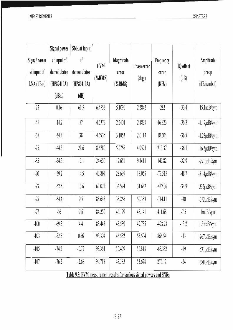
MEASUREMENTS CHAPTER 9
Signal power SNR at input
Signal power at input of of Magnitude Frequency Amplitude EVM Phase error IQ offset
at input of demodulator demodulator error error droop (%RMS) (deg.) (dB)
LNA(dBm) (HP89410A) (HP89410A) (%RMS) (KHz) (dB/symbol)
(dB m) (dB)
-2) 0.16 605 6.47)3 ).1090 2,2~42 -2~2 -33.4 -1),lndB/sym
-45 -14.2 57 4.6377 2,6401 2.1~37 46,~23 -36.3 -1.l7 ~dB/sym
-65 -34.4 3~ 4,6935 3.1053 2,0114 1~,604 -365 - 1.23~dB/sym
-7) -44,3 29,6 ~,6nO 5,0756 4,0573 213,37 -36.1 -56,3~dB/sym
-~5 -54.5 19.1 24,650 17,651 9,~411 149,~2 -32,9 -291~dB/sym
-90 -59.2 145 40,~04 2~,699 1~,055 -7751) -4~,7 -~1.4~dB/sym
-93 -62.5 10,6 60,073 34.574 31.6~2 -427,06 -34,9 335~dB/sym
-9) -64.4 95 ~~,64~ 3~,266 50,3~3 -714.11 -40 -652~dB/sym
-97 -66 7,6 ~4.250 46.179 4~.141 411.6~ -75 1mdB/sym
-lOO -69.5 4.4 ~~.443 455~9 49.7~5 -493.73 -13.2 l.5mdB/sym
-103 -72.5 0,66 93,304 46552 53.504 ~66.54 -l3 -267~dB/sym
-105 -74.2 -0,72 93,361 50.409 )O,~1~ -65,332 -19 -531 ~dB/sym
-107 ·76.2 ·2,6~ 94,71~ 47,3~3 53.6n 276.12 -24 . 3~0~dB/sym
Table 9.5: EVM measurement results for various signal powers and SNRs
9-27

MEASUREM ENTS CHAPTER 9
Figures (9.20) to (9.23) show various plots extracted from table (9.5). Figure (9.20)
shows a plot ofLNA input signal power versus SNR. An intuitive obvious trend here
is that an increase in the signal level at the input of the LNA causes an increase in the
SNR (at the input of the HP89410A). Signal levels between - 107dBm and -25dBm
produce SNRs in the range - 2 .7dB to 60.5dB. However, it should be noted that the
SNRs start to level-off at the lower and upper extremes of signal power. The
levelling-off at the lower extreme (input signal power < -I OOdBm) can he attributed to
the signal level reaching the noisefloor of the instrument. The levelling-ofT at the
upper extreme (input signal level > -45dBm) can possibly be due to the HP89410A
being overdriven by the receiver RF front-end. There is a high probability that the
"ranging" calibration procedure for the HP89410A, for these power levels, was
omitted.
65 ·~H=+=l==+~::r-=F=r ss +-- ___ g 45 +--+-+--I-+-IV----~-f-+-j ~ 35
~ 2S
'" IS ., 5 I-.. -+ ... ~r_-+--+-t_+__ +-+__-1
-5 ~~~~~~-~---~~~
-115 -105 -95 -85 -75 -65 -55 -45 -35 -25
LNA input signal power (dBm)
Fig. 9.20: LNA input signal power versus SNR
A plot ofSNR versus EVM is shown in figure (9.21). The general trend, once again
here, is an increase in SNR causes the EVM to decrease. EVM values between
4.6% RMS and 94.7% RMS are produced for SNRs in the range - 2.7dB to 60.5dB.
Figures (9.22) and (9.23) show plots of SNR versus magnitude error and SNR versus
phase error, respectively. The magnitude error increases from 5. 1 % RMS to
47.4% RMS for a decrease in the SNR from 60.5dB to - 2.7dB. The phase error
varies between 2° and 53.7° for the same range of SNRs. It is evident from figures
(9.21) to (9.23) that the EVM (and hence the magnitude and phase errors) do not
exhibit a regular trend for a SNR range of between - 3dB to 9.5dB. This irregularity
may possibly be due to the sensitivity limitation of the HP89410A (the signal levels
9-28

MEASUREMENTS CHAPTER 9
corresponding to this range of SNRs may be approaching the nOise floor of the
instrument).
-'" :;:
'" ... ~
:;: > '"
100 90 80 70 60 50 40 30 20 10 0
-5
Vi :;: 55 '" 50 ~ 4S
• 35 e 30 t 25 ~ 20 ~ IS c 10 '" 5 • 0 :;:
-5
5 15 25 35 45
SNR (dB)
Fig. 9.21: SNR versus EVM
5 15 25
~ ,
35
SNR (dB)
45
55
55
Fig. 9.22: SNR versus magnitude error
" - 50 -• .
~ 40 • 35 e 30 t; 2S ~ 20 ~ 15 s: 10
5 o -5 5 15 25 35 45 55
SNR (dB)
Fig. 9.23: SNR versus phase error
9-29
65
65
65

MEASUREMENTS CHAPTER 9
The importance of an LNA in the receiver RF front-end has been emphasized in the
simulation results of chapter 5. The measurement results in table (9.6) conclusively
verifies this importance for a - 90dBrn signal power into the receiver RF front-end.
As can be seen, the use of an LNA not only causes an improvement in the SNR but
also a decrease in the magnitude and phase errors and hence a decrease in the EVM.
Signal power SNR at input Magnitude
into of EVM Phase error
demodulator demodulator (% RMS) error
(HP8941 0A) (HP8941 0A) (% RMS)
System -59.2dBm 14.5dB 40.804 28.699 18.055·
with LNA
System
without -81.5dBm 3.ldB 99.073 51.323 57.150·
LNA . . . Table 9.6: Comparison of EVM results for sYstem with and without LNA
9.5 Conclusion
This chapter has supported the theory and simulation results of the preceding chapters
through the implementation of a receiver RF front-end for a BPSK system. Using the
phase noise theory in chapter 6 in conjunction with the HP89410A vector signal
analyzer, a quantitative phase noise comparison of two frequency sources were
perfonned. The phase noise density profiles were used to extrapolate the single
sideband levels. Hence by use of equation (6.49) in chapter 6, the single sideband
noise-to-signal ratios or variance (crT2) were computed. Variance values of -40.5dB
and -66.4dB were obtained for these frequency sources (at a frequency of 5MHz),
allowing a comparison to be made.
In chapter 5, the BER was used as a figure of merit to evaluate the effect of RF
component noise. In this chapter, a different figure of merit, the EVM, was used for
this purpose. In chapter 5, it was established that RF component noise as a result of
the noise figure) causes degradation of the SNR and hence an increase in the BER.
These range of SNRs were replicated (to an extent) in the measurement setup to
evaluate the effect of RF component noise. The general trend from the results is that
9-30

MEASUREMENTS CHAPTER 9
an increase in the SNR causes the EVM to decrease, and vice-versa. EVM values
between 4.6%RMS and 94.7%RM:S are obtained for SNRs in the range - 2.7dB to
60.5dB. Only a quantitative comparison between the simulated CDMA setup (chapter
5) and the implemented BPSK setup can be made. Linking these SNR values to the
simulation setup and results of chapter 5 (figure (5 .11)), a SNR of 4.42dB corresponds
to an LNA noise figure of 3dB (LNA gain = I3dB and mixer noise figure = 5dB).
Figure (9.24) shows a trace of the symbol and error summary (after demodulation) for
512 bits. This is the maximum number of bits that can be displayed for BPSK
demodulation (with 1024MB RAM and a minimum sampling rate of 2 samples per
symbol, the maximum number orbits that can be displayed by the HP89410A is 512).
TRACE A: Chl BPSK S~~I:s/Err5 A Murk<l:r 45 00000 5::1 11 . 1 0000 .
EV" ~ ~8J8~ Xrl'ts 18Uil x pit at OYM <~ Mug Err XrMS x pit o,t SYM Phase Err = 51.897 de. -89.95q de. pk at OYM q75 Fre:q Err = -q93.73 kHz 1 Q Offset = -13.182 d8 AHP Droop = 1."169 I1d8/s)l11
o mt 00011001 111 10000 0000011 1 11000111 001111"1 1
"18 11111110 11010111 11 111111 10111011 11 10 1 11 96 1 111111 I 1111 11 0 1 11111 101 11 111111 11111111
1 "1"1 1 1 11 11 1 1 11111111 11111111 11111111 11111111 192 111111 0 1 11111111 11110111 tll1l111 11111111 2.0 11111111 11111111 11111111 11111111 11111111 288 10111011 10 111000 0101111 1 11101010 01001111 336 11101000 0 100 1010 01010010 00000001 01000000 38. n 01000000 00000000 01000 1 00 010000 11 00000000 q32 00 1 00000 00000000 00000001 00000o 1 0 00 11 1100 Q80 01000011 0001 1000 10000010
Fig. 9.24: Symbol and error summarv for SNR of4.4dB (at input of HP89410A)
and - IOOdBm LNA input power
Figure (9.24) shows the errors for a SNR (al the input of the HP89410A) of 4.4dB
corresponding to an LNA input power (see block diagram of figure (9.1)) of -
lOOdBm. From this trace, 238 out of the 512 bits are in error. For a realistic bit
length of 109, this translates to a best-case BER of 5.12 x 10⁻⁷
. However, the CDMA
simulation setup in chapter 5, yielded a BER of7.6 x 10-12 for the same SNR (figure
(5.13)). Recall that the simulation setup consisted of spread (or chipped) data BPSK
modulating a RF carrier and the BER measurement was perfonned on the received
data after the despreading process. In contrast, this measurement setup consists solely
9·31

MEASUREMENTS CHAPTER 9
of data BPSK modulating a RF camer and the BER computed after camer
demodulation. Essentially, the BER computed from the measurement is the simulated
CDMA system equivalent of "chip error rate". Thus it can be concluded that the
effect of RF component noise is more severe in a non-CDMA BPSK system than in a
CDMA system employing BPSK modulation. CDMA' s ability to suppress in-band
interference and noise through its processing gain is apparent.
Methodologies for troubleshooting the RF front-end using EVM were also discussed.
Signal quality was demonstrated visually using IQ constellation diagrams. The
effects of filtering were also shown using IQ vector diagrams. These diagrams
con finned that filtering smoothens the transitions between states (chapter 4). EVM
results from table (9.6) also conclusively verified the theoretical and simulation
importance of an LNA in the receiver RF front-end (chapter 5).
9-32
CQNCLUSIONS CHAPTER 10
CHAPTER 10
CONCLUSIONS
10.1 Summary and conclusions
This thesis examined the topic of design considerations and implementation of a RF
front-end for a CDMA adaptive array system. A detailed study of the RF
implementation issues were presented, beginning with a literature SUlvey on antenna
arrays and beamfonning in chapters 2 and 3 and ending with an implementation and
evaluation of a receiver RF front-end for a BPSK transceiver system in chapter 9.
A li terature survey on antenna arrays and beamfonning was presented in chapters 2
and 3. In chapter 2, the basic concepts of antenna arrays (specifically the linear array)
were described. Also discussed were the principles of beamscanning, pattern
multiplication and antenna element spacing criteria for the avoidance of grating lobes.
All these concepts were demonstrated by a simulation that plots the array beam
pattern as a function of the number of elements, element spacing and scan angle using
a half wavelength dipole as the antenna element. Amongst the conclusions that can be
drawn out from this simulation are: an increase in the number of antenna elements
increases the main beam directivity of the array response (increase in gain and
decrease in main beamwidth). However, it also results in an increase in the number of
sidelobes in the total pattern.
Chapter 3, was essentially a li terature survey of analogue and digital beamfonning
and the implementation implications of adaptive antennas at RF, [f or baseband. An
adaptive beamfonning configuration for COMA (using Compton's loop) and the
implementation issues thereof were described. Due to the fact that each CDMA user
would require a separate loop, it would be cost-effective in a multi user system to
implement this loop in software in baseband. The loop can also be implemented at [f
using hardware followed by digital processing. This setup not only places increased
requirements on the digital processor (which now has to process a much higher
10-1

CONCLUSIONS CHAPTER 10
frequency signal), but is also costly in a multi user system where hardware would be
required for each user. The loop cannot be processed at RF (digital technology at RF
is awaited). Although analogue beam forming and loop implementation (using
hardware) can be performed at RP, the RP error signal would not be able to be
processed by a present-day adaptive processor. Hence RF adaptive beam forming of
the above loop is presently impossible. However, the weights themselves can be
implemented in hardware using analog phase shifters and attenuators at either RF
(following the antenna elements) or IF (following the IF amplifiers). The processing
of the weights in this case can be performed at basebandlIF. In a large array. this setup
is costly and increases the complexity of the front-end. The best alternative is to
perform adaptive beamforming at baseband with the weights being implemented
digitally in software.
An overview on COMA theory and concepts were provided in chapter 4. Issues such
as its background, advantages over other multiple access schemes and the all
important process of filtering was also included. The COMA theory and concepts in
this chapter were demonstrated by simulation work using Advanced Design System
(ADS) software. The work here formed the basis for the simulation models utilized in
the latter chapters of this thesis.
Chapter S investigated the effect of internally generated RF component noise on the
bit error rate of a DS-COMA system. Essentially, RF component noise (as a result of
component noise figure) cause degradation of both the ratio of energy per bit to noise
power spectral density (EJNo) and the signal-to-noise ratio (SNR) and hence an
increase in the bit error rate (DER). The importance of an LNA tu establish the system
noise figure was confinned via simulation. For the proposed system (processing gain
of 42) utilizing an LNA, the BERs are between 7.7x 10⁻³ and 7.6x 1 0-12 for mixer noise
figures in the range SdB to lSdB. However, without an LNA, the BERs range from
2.8xI0-2 to 2.7xI0-1 for the same range of mixer noise figures. For the proposed
system (utilizing a mixer with 5dB conversion loss/noise figure), Et/No and SNR
improvements of 9.S3dB are obtained over the same system without an LNA. Also
EJNo and SNR improvements in the range 9.53dB to 12.51dB are obtained for mixer
noise figures from SdB to lSdB. The simulation also concluded that the use of
commercially available RF components in the front-end do not cause severe BER
10-2

CONCLUSIONS CHAPTER 10
degradation in a single-user DS-CDMA system. In a worst-case, highly improbable
scenario, an LNA gain as low as 3dB and noise figure as high as 13dB produce BERs
of 7.5x I 0.3 and 12.9x I 0.3• respectively for a modest processing gain of 42. It can be
anticipated that the effect of RF component noise in a multi-user DS-CDMA
environment would be much more severe than that of the single-user case. Multiuser
interference (MJ) would cause a decrease in the SNR and hence an increase in the
BER.
Chapter 6 examined the impact of local oscillator generated phase noise on DS
CDMA performance. A thorough discussion and analysis of phase noise from an RF
engineer's perspective was initially provided. This was followed by simulation work.
For the proposed system ( IOdB SNR at the input of the LNAl, phase noise variance in
the range - 16.5dB to -3.3dB produce BERs in the range 10" to 0.5 1 for the system
processing gain of 42. Phase noise variance less than - 16.5dB produce negligible
BERs (in the order of 10.24) . For a 7dB SNR at the input of the LNA, variance in the
range - 20.6dB to - 3.3dB produce BERs between 0.51 and 10" (same BERs as 10dB
SNR but for larger variance range). Negligible BERs (in the order of 10'24) are
produced for variance values less than - 20.6dB. However, with a SNR at the input of
the LNA of 5dB, phase noise variance between - 39.4dB and - 3.3dB produce BERs
between 7x 1 0-4 and 0.51. These results indicate that the BER degradation due to
phase noise is more severe for lower SNRs. By comparing the phase noise variance of
commercially available oscillators with these variance ranges, it can be concluded that
the phase noise perfonnance of typical oscillators have negligible effect on the BER
of the proposed system (input SNR of 10dS and processing gain of 42). This was
substantiated in chapter 6 by considering that the IF phase noise power (N/F) exists in
the same proportion to the RF receiver power, PRF (at the RF input of mixer) as the
phase noise was to the oscillator power if it passes through no narrowband filtering
capable of limiting its bandwidth ( N1FldB
" :: P/U-,ldB
.. -SNRwldB
). However, the effect of
phase noise has different degrees of impact on the system's performance dependent
on the PSK modulation type. This is intuitive from the signal-space representation of
various PSK formats. The higher the PSK modulation format, the greater is the impact
of phase noise. Thus it can be concluded that, in general, it is unnecessary for
oscillator specifications to be overly restrictive in terms of phase noise. However,
to-3

CONCLUSIONS CHAPTER 10
being overly restrictive with this phase noise specification, places less demand on the
low-noise design of other components in the RF system.
An overview on mixer theory was presented in chapter 7. As mentioned previously,
due to its extensive presence in the previous chapters, a single chapter on this device
was warranted. Its functionality and presence have been highlighted in chapters 3, 5
and 6. In chapter 3, frequency downconversion has made the digital adaptive array
receiver realizable. Downconversion was necessitated to make use of currently
available digitization and processing hardware. Mixers have also been encountered in
chapters 5 and 6. The results of the investigation on the effect of RF component noise
(in chapter 5) were hinged around the mixer noise figure since it has been quoted as
being the dominant source of noise and distortion in the receiver. The topic of local
oscillator phase noise was considered in chapter 6. Being an inseparable entity of the
mixing process, the LO phase noise that leaks from the LO port to the IF port of the
mixer, was considered. So, it is not surprising that a single chapter was devoted to
some mixer theory. The theory and understanding of some concepts in this chapter
provides some insight into the implemented BPSK RF front-end of chapter 9. Most of
these concepts are often taken for granted. For example, the simple concept of sum
and difference frequencies, enable selection of the appropriate LO frequency for a
given RF and desired IF. Also through discussion and simulation of intermodulation
products. the importance of an IF bandpass filter (to reject unwanted intermodulation
products) in this BPSK system becomes apparent. Furthermore, the non-linear mixing
process also provides a reason for the LO drive level always being specified higher
than the RF level in manufacturer's datasheetslcatalogues.
The contents of chapters 8 and 9 constituted the RF design and implementation
sections of this thesis. Chapter 8 was dedicated to the design, simulation, construction
and characterization of a low noise microwave amplifier originally intended to
quantify its performance in the BPSK RF front-end (chapter 9). However, the noise
figure of this LNA could not be measured thus prohibiting its performance evaluation
in the BPSK system. Nonetheless, a low-cost, in-house 2GHz broadband LNA with
13. 1 dB gain and 520MHz 3dB bandwidth, for possible use in the proposed CDMA
adaptive array system, was developed. The specifications were defined as: 2GHz
center frequency, required operating power gain:;?; 10dB, minimum 3dB bandwidth of
10-4

CONCLUSIONS CHAPTER 10
lOMHz, noise figure less than 3dB in this lOMHz bandwidth (corresponding to the
typical range of noise figures of commercially-available LNAs). This lOMHz
bandwidth is commensurate with the 4.096MHz chip rate of WCDMA - a bandwidth
of 8. I92MHz (2 x chip rate) is required for BPSK modulation. On design and
simulation of the initial circuit, the simulation results revealed a transducer gain
(I S211) of 12.89dB at 2GHz, 3dB bandwidth of approximately 400MHz and a noise
figure less than 3dB within an approximate bandwidth of 1.250Hz. Although these
results met the specifications, the large value of the input renection parameter (I Sil l)
of - 7.906dB was undesirable. Thus there was a need to optimize the initial circuit for
an improved input match (lower input reflection parameter). An optimum input
reflection parameter of - 26.765dB was obtained by reducing the quarter-wave
transformer length (between the 50n input line and input open circuit stub) from
22.334mm to 13.867mm. This was achieved by using the optimization tuning tool in
ADS. In addition to the improved input match, optimization also resulted in a
marginal improvement in gain (I S21 1) from 12.89dB to 13.793dB and a decrease in
the noise figure from 1.858dB to 1.655dB (@2GHz). The 3dB bandwidth was greater
than 200MHz while the noise figure was less than 3dB within a 1.6GHz bandwidth
still well within the amplifier specifications. Finally, this optimized circuit was
constructed and characterized. There was good correlation between the simulated and
measured s-parameter results, with the exception of the measured input reflection
parameter (I Sil l ~ - 15.877dB). This can possibly be attributed to the non
consideration of the biasing lines, step-width change discontinuity, coupling and
bypass capacitors in the simulation model. Nevertheless, an input reflection
parameter of - 15.877dB is acceptable. The gain of the amplifier was measured to be
13.ldB whi le the 3dB bandwidth was computed as 520MHz. Thus a broadband
design has been achieved (Q factor of 3.85). Noise figure measurements were
perfonned using the HP346B noise source and the HP8970B noise figure meter. The
theory and operation behind these instruments were discussed. Unfortunately, no
correlation/comparison between the simulated and measured noise figure (at the
desired frequency of 2GHz) could be made. This was due to the 1.8GHz operating
frequency limitation of the HP8970B noise figure meter. At 1.8GHz, the noise figure
of the ampli fier was measured to be 2.7dB. A low-cost, in-house, operational LNA
10-5
CONCLUSIONS CHAPTER 10
was achieved in this design. The theoretical and practical aspects of LNA design has
been presented in this chapter.
In chapter 9, a receiver RF front-end, excluding the antenna (using off-the
shelf7comrnercially available components) for a BPSK transceiver was implemented.
The objective of this chapter was to support or reinforce the theory of the preceding
chapters (specifically chapters 5 and 6). The chapter began with a description of the
system. Waveforms for most of the stages were shown. The gain, conversion loss or
insertion loss for each of the RF components were measured. The overall gain of the
front-end was computed to be approximate ly 23.6dB. By using the specified noise
figure (from the manufacturer's datasheet) for each component and the measured
gain. the overall noise figure was computed to be 1.873dB. The focus of the next
subsection was on phase noise measurements. Here, two techniques, the delay line
method and the phase detector method, for measuring phase noise were discussed.
However, a straightforward technique, using the HP89410A vector signal analyzer.
was employed for the phase noise measurements. The phase noise perfomlance of
two Rohde and Schwarz frequency sources (models SMIQ 03 and SMS) were
compared. The power level and frequency of both sources were set to 10dBm and
5MHz, respectively. The phase noise density profiles (represented in teons of the
power spectral density of phase fluctuations, S;(f) were obtained. From these the
single sideband level versus offset frequency were extrapolated. By use of equation
(6.49) in chapter 6, the single sideband noise-to-signal ratio or variance (ui) were
computed. This was calculated for 3 line segments (0 = 3) Le. the phase noise density
profile was approximated by 3 line segments. Variance values of -40.5dB and
-66.4dB were obtained for the SMS and SMIQ 03 models, respectively. A
quantitative phase noise comparison of these frequency sources could thus be made.
The laner part of chapter 9 was dedicated to Error Vector Magnitude (EVM)
measurements, using the HP89410A vector signal analyzer. In addition to providing a
figure of merit for a digitally modulated signal, it also helps to identify the type and
source of signal degradation by using different troubleshooting methodologies. The
section began with a definition of EVM followed by a description of a troubleshooting
tree that can be used as a guideline to troubleshoot digital RF communication systems.
Some of these troubleshooting methodologies were demonstrated on the BPSK
10-6

CONCLUSIONS CHAPTER 10
transceiver system. In chapter 5, it was established that RF component noise (as a
result of component noise figure) cause degradation of the SNR and hence an increase
in the BER. SNR values within the same range as used in the simulation were
replicated for the measurement setup. The signal level at the input of the LNA was
varied between - 25dBm and - 107dBm. producing SNRs at the input of the
demodulator (HP89410A) between 60.5dB and - 2.7dB. The general trend, is an
increase in SNR causes the EVM to decrease. EVM values between 4.6% RMS and
94.7% RMS are produced for SNRs in the range - 2.7dB to 60.5dB. The magnitude
error increases from 5.1 % RMS to 47.4% RMS for a decrease in the SNR from
60.5dB to - 2.7dB. The phase error varies between 2° and 53.7° for the same range of
SNRs. By linking a particular SNR value to the SNR value in the simulation setup
and results of chapter 5, a quantitative comparison between the simulated CDMA
setup (chapter 5) and the implemented BPSK setup could be made. This revealed that
the effect ofRF component noise is more severe in a conventional BPSK system than
in a CDMA system. IQ constellation diagrams were used to demonstrate the quality
of modulated signals. IQ vector diagrams were used to demonstrate and confinn the
effects of filtering. The system with root raised cosine filtering (a = 0.5) and without
filtering (a. = 00) were compared. These diagrams confirmed the theory in chapter 4
that filtering smoothens the transitions between states. The importance of an LNA in
the receiver RP front-end has been emphasized in the simulation results of chapter 5.
The measurement results conclusively veri fied this importance: the use of an LNA not
only causes an improvement in the SNR but also a decrease in the magnitude errors.
phase errors and hence a decrease in the EVM. For the system without an LNA, the
EVM was measured to be 99.1 % RMS while with an LNA it was 40.8% RMS. The
magnitude errors were 51.3% RMS anu 28.7% RMS for systems without and with
LNA, respectively. The corresponding phase errors were 57 .2° and \8.1 °.
10.2 Possible extensions and topics of further study
Finally, to conclude this thesis. some possible extensions and/or further topics of
study to this research are presented:
(a) The first part of this thesis presented a literature survey on antenna arrays and
beamforming. No mention of the type of antennas used in cellular
communications were made. The choice of antennas for the array are important
10-7

CONCLUSIONS CHAPTER 10
and depends on the requirements that need to be satisfied. Some of the
requirements that need to be considered are their gain, coverage pattern, the power
available to drive them and polarization. As a possible extension, further research
on these aspects is proposed.
(b) The simulation model for the generation of the array beam pattern in chapter 2
did not take into account the effects of mutual coupling. Similarly, it is suggested
that an expression (incorporating the effects of mutual coupling) for the array
factor be derived. This expression will depend on the antenna element type.
(c) Furthermore, in the investigation in chapter 5, it may be of interest to evaluate the
BER degradation as a result of overdriving the receiver RF front-end into
compressIon.
(d) Considerat ion should also be given to extend the phase noise simulation model
(in chapter 6) to a multiple carrier (MC) environment. Although the existing DS
COMA model, in effect, used a typical loaded SNR of IOdB, it would be
interesting to study the impact of LO-generated phase noise in a MC-CDMA
system. Although documented in the literature, the existing theory and
understanding would be enhanced.
(e) A "hardwired" BPSK transceiver was implemented and documented in chapter 9.
Recall, initially it was intended to utilize the Alcatel software radio as the CDMA
transceiver platform. However, the carrier demodulation process is not supported
by this radio. As a result, the HP8941 OA vector signal analyzer was used for this
purpose. As mentioned previously, there are two downsides to this instrument:
• The HP894 10A is incapable of demodulating a CDMA signal i.e. it cannot
perform the despreading operation. Thus, the idea of implementing a simple
BPSK transceiver was conceived.
• The demodulated signal is not available as an analog output or bitstream for
analysis. Thus, BER measurements are not possible with this instrument.
For the above reasons, it is proposed that research towards the implementation of
a carrier demodulator, be conducted. It is envisaged that such demodulation
10-8

CONCLUSIONS CHAPTER 10
circuitry would interface with the software radio, completing the missing link, to
foml a complete CDMA transceiver. The performance of the receiver RF front
end in a CDMA environment can thus be evaluated. Another possible future
extension will involve the performance evaluation of the receiver RF front-end in
a wireless CDMA environment (including the effects of multi path and fading).
10-9

REFERENCES
REFERENCES 1. T. Ojanpera and R. Prasad, "Wideband CDMA for third generation mobile
communications," Artech House, Norwood, 1998.
2. S. Anderson, M. Miinert, M. Viberg and B. Wahlberg, "An adaptive array for
mobile communication systems," Trans. on Veh. Tee. , Vol. 40, 199 1.
3. S.C. Swales, MA Beach, DJ . Edwards and l.P. McGeehan, "The
performance enhancement of multihearn adaptive base-station antennas for
cellular land mobile radio systems," IEEE Trans. Veh. Technol., va l. 39, p56-
57, 1990.
4. Shiam-Shiun Jeng et aI, "Experimental evaluation of smart antenna system
performance for wireless communications," IEEE Trans., Vel. AP-46, June
1998, P749-757.
5. I.S. Thompson, P.M. Grant, B. Mulgrew, "Smart antenna arrays for CDMA
systems," IEEE Personal communications, Vol. 3 (1996), PI6-25.
6. Yingjie Li , Martin J. Feuerstein, Douglas O. Reudink, "Perfomlance
evaluation of a cellular base station multibeam antenna," Trans. ffiEE Veh.
Tech., Vo1.46, no. I, Feb. 1997, PI-9.
7. Agi lent Technologies Advanced Design System release 1.3: This is an
electronic design automation (EDA) software that allows design, simulation,
optimization and verification of DSP, RFIC, communication systems, RF
board, microwave and electromagnetic designs.
8. Bemard D. Steinberg, "Principles of aperture and array system design," John
Wiley and sons, New York, 1976.
R-I
REFERENCES
9. Richard C. lohnson and Henry Jasik. "Antenna applications reference guide,"
McGraw-Hill, New York, 1987.
10. J.E. Hudson, "Adaptive array principles," Short Run Press Ltd. , England,
1981.
11. C.A. Baianis, "Antenna theory, analysis and design," 2nd edition, John Wiley
and sons, New York, 1997.
12. L.C. Godara, "Application to antenna arrays to mobi le communications,
part I: perfonnance, feasibility, and system considerations," Prae. IEEE. Vel. 85,
July 1997, P1029-1060.
13. Robert A. Monzingo and Thomas W. Miller, "Introduction to adaptive arrays,"
John Wiley and sons, New York, 1980.
14. L.C. Godara and A. Cantoni. "Uniqueness and linear independence of steering
vectors in array space," 1. Acollst. Soc. Amer. ,Vol. 70, P467 - 475 ,1981.
15. A.F. Naguib, A. Paulraj, and T. Kailath, "Capacity improvement with base
stat ion antelUla arrays in cellular CDMA," rEEE Trans. Veh. Technol. , Vol.
43, P691 - 698, 1994.
16. D.G. Brennan, "Linear diversity combining techniques," Proc. IRE. , Vol. 47,
PI075 - 1102, 1959.
17. J. Litva and T.K.Y. Lo, "Digital beamfonning in wireless communications,"
Artech House, Inc., 1996.
18. Paul H. Young, " Electronic Communication techniques," fourth edition,
Prentice Hall , 1994.
19. A.R. lopez, "Pcrfonnance prediction for cellular switched beam intelligent
antenna system," IEEE commun. Mag. , Vol. 34, P152-154, Oct 1996.
R-2

REFERENCES
20. B. Suard, A.F. Naguib, G. XU and A. Paulraj, "Performance of CDMA mobile
communication systems using antenna arrays," Proc. IEEE Int. Conf.
Acoust.,Speech and Signal processing (ICASSP), Minneapolis, MN, 1993,
PI53-156.
21. Y.Wang and J.R. Cruz, "Adaptive anteIUla arrays for the reverse link of
COMA cellular communication systems," lnst. Elect. Eng. Electron. Lett. ,
Vo1.30, PI017-1018, 1994.
22. Robert 1. Mailloux, "Phased array antenna handbook," Artech House, Boston,
1994.
23. Robert C. Hansen, "Microwave scanrung antennas," Peninsula publishing,
California, 1985.
24.1.0. Kraus, "Antenna alTays with closely spaced elements," Proc. IRE, Vol.
28, P76-84, February 1940.
25. Lamont V. Blake, "Antennas," John Wiley and sons, New York, 1966.
26. J.L. Alien, "Gain and impedance variation in scanned dipole arrays," LEEE
Trans. on antennas and propagation, AP-IO, no.5, P567-569, September 1962.
27. M. Barren and R. Amott, "Adaptive antennas for mobile communications,"
Electron. Commun. Eng. l., Vol. 6, P203-214, 1994.
28. B. Widrow et ai, "Adaptive antenna systems," Proc. IEEE, Vol. 55, Oec.1967,
P2143-2159.
29. W.F. Gabriel , "Adaptive arrays - an introduction," Proe. IEEE, Vol. 64,
February 1976, P239-272.
R-3
REFERENCES
30. James Bao-Yen Tsui, "Digital microwave receivers - theory and concepts,"
Artech House, Norwood, 1989.
31. Butler J.L. and Lowe R. , "Beamfonning matrix simplifies design of
electronically scanned antennas," electronic Design, Vol. 9, Apr. 12, 1961 ,
PI70-173.
32. RC. Hansen, "Phased aTTay antennas," John Wiley and sons, New York, 1998.
33. M. l. Skolnik, "introduction to radar systems," 2nd edition, McGraw Hill book
company, New York, 1980.
34. Raymond Tang and Richard W. Bums, "Phased aTTays," from "Antenna
engineering handbook," by R.C. Johnson and H. Jasik, 2nd edition, McGraw
Hill, New York, 1984, P20-1 to 20-67.
35. Edward A. Wolff and Roger Kaul, "Microwave Engineering and system
applications," John Wiley and sons, U.S.A., 1988.
36. R.D. Gaudenzi, "The influence of signal quantization on the perfonnance of
digital receivers for CDMA radio networks," ETT, VoL 8, No. I, January -
February 1997, P89 - 97.
37. F.G. Weiss, "A IGs/s 8-bit GaAs ADC with on-chip current source," Proc.
GaAs IC Symposium, P209, 1986.
38. T. Dcourant et al., "3GHz, 150mW, 4-bit GaAs analog to digital converter,"
Proc. GaAs IC Symposium, P301-304, 1986.
39. B.P. Del Signore, "Monolithic 20-b delta-sigma AID converter implemented
in standard 3~m CMOS technology,"lEEE J-SC, Vol. 8, Dec. 1990.
R-4

REFERENCES
40.1. Valburg, "8-b 650MHz folding AID converter with analog error correction,"
IEEE J-SC, Vol. 10, Dec. 1992.
41. H. Kimura, "IO-b 300MHz interpolated-parallel ADC implemented in double
polysilicon self-aligned bipolar technology," IEEE J-SC, Vol. 11, Apr. 1993.
42. A.N. Karanicolas, "15-b I Msample/s digital self-calibrated pipeline ADC,"
IEEEJ-SC, Vol.ll,Dec. 1993.
43. C. Schiller, "40Hz 8-bit ADC system uSlllg sample and filter sampling
techniques," IEEE J-SC, Vol. 9, Dec. 1991.
44. F. Goodenough, "ADCs become application specific," Electronic Design, P42-
50, Apr. 1993.
45. E.O. Brigham, "The fast fourier transform and its applications," Prentice-Hall ,
Englewood Cliffs, NJ, 1988.
46. Taub and Schilling, "Principles of communication systems," 2nd edition,
McGraw-Hill Book company, Singapore, 1986.
47. R.T. Compton, "An adaptive antenna in a spread spectrum communication
system," Proc. IEEE, vol. 66, March 1978, P289-298.
48. R.T. Compton, RJ. Huff, W.G. Swamer and A.A. Ksienski, "Adaptive arrays
for communication systems: An overview of research at the Ohio State
University," IEEE Trans. Antennas Propagation, Vol. AP-24, P599-607, 1976.
49. E. Bouktache, "On the stability of adaptive antenna arrays with weights at an
intermediate frequency," rEEE Trans., Vol. AP-40, November 1992, P1438-
1444.
50. Dean E. Svoboda, "A phase-locked recelvmg array for high-frequency
communications use," IEEE Trans., Vol. AP-12, March 1964, P207-215.
R-5

REFERENCES
51. Jonas Strandell et ai, "Experimental evaluation of an adaptive antenna for a
TDMA mobile telephony system,"
52. Y.J. Guo, S. Vadgama, M. Davies, J. Khalab, M. Zarri and D. Spink, "An
adaptive antenna for CDMA," IEEE 5th International symposium on spread
spectrum techniques and applications, Sun City, South Africa, 2-4 September,
1998.
53. Joel L. Dawson, Jenshan Lin, "An adaptive antenna integrated with automatic
gain control for receiver front end," IEEE MTT-S International Microwave
Symposium Digest , Vol. 3, June 1997.
54. Kimmo Kalliola and Pertti Vainikainen, "Characterization system for radio
channel of adaptive array antennas,"
55. Tom Gratzek, Brad Brannon, Jim Camp and Frank Murden, "A new paradigm
for base station receivers: High IF sampling + digital filtering," IEEE radio
frequency integrated circuits (RFIC) Symposium, June 1997.
56. F. Swarts, P. van Rooyan, I. Oppennann and M.P. Lotter, "CDMA techniques
for third generation mobile systems," Kluwer Academic Publishers, U.S.A.,
1999.
57. Samuel C. Yang, "CDMA RF system engineering," Artech House, Inc.,
Norwood, 1998.
58. Vijay K. Garg, Kenneth Smolik, Joseph E. Wilkes, "Applications of CD MA in
wireless/personal communications," Prentice-Hall NJ, 1997.
59. Lilja H., "Characterizing the effect of nonlinear amplifier and pulse shaping
on the adjacent channel interference with different data modulations,"
Licentiale Thesis, Oulu University. Finland, 1996.
R-6

REFERENCES
60. Asha Mehrotra, "Cellular radio perfonnance engineering," Artech House, [nc.,
Norwood, 1994.
61. F.R. Connor, "Noise," 2nd edition, Macmillan India Ltd., Bangalore, 1982.
62. Nyquist H., "Thennal agitation of electric charge In conductors," physical
review, Vol. 32, PlO, 1928.
63. Peter C.L. Vip, "High-frequency circuit design and measurement," 1st edition,
Chapman and Hall, 1991.
64. www.mprg.ee.vt.edulresearchlglomo/antennalarch.html
65. Lawrence E. Larson, "RF and microwave circuit design for wire less
conununications/' Artech House, Norwood, 1996.
66. D. Lu and K. Yao. "Improved importance sampling technique for efficient
simulation of digital communication systems," LEEE J. Selet. Areas Commun .•
Vol. 6, P67 - 75, Jan. 1988.
67. D. Lu and K. Vao. "Estimation variation bounds of importance sampling
simulations in digital communication systems." IEEE Trans. Commun., Vol.
39,PI413 - 1417, Oct.1991.
68. J. Chen, D. Lu, J. Sadowski and K. Vao, "On importance sampling in digital
conununications - Part 1: fundamentals," rEEE 1. Select. Areas in Commun.,
Vol. 1I, No. 3, P289-299, April, 1993.
69. P.F. Combes, J. Graffeuil, J.F. Sautereau. "Microwave components, devices
and active circuits," John Wiley and sons Ltd., Great Britain, 1987.
70. Stephen A. Maas, "Microwave mixers," 2nd edition, Artech House, Norwood.
1993.
R-7
REFERENCES
71. Vadim Manassewitsch, "frequency synthesizers theory and design," second
edition, John Wiley and sons, 1980.
72. "The American Radio Relay League Handbook (ARRL)" 1998.
73. T. Pollet, M. Van Bladel and M. Moeneclaey. "SER sensitivity of OFDM
systems to carrier frequency offset and Wiener phase noise," IEEE Trans.
Commun., Vol. 43, PI91-193, Feb./Mar.lApr., 1995.
74. P. Robertson and S. Kaiser, "Analysis of the effect of phase nOise m
orlhogonal frequency division multiplex (OFDM) systems," in Proc. ICC'95,
Seatlle, WA, June 1995, PI652-1657.
75. L. Tomba and W.A. Krzymien, "Sensitivity of the MC-COMA Access scheme
to carrier phase noise and frequency offset," IEEE Trans. On Veh. Tech., Vol.
48, no. 5, September 1999, PI657-1665.
76. U.L. Rohde, "Digital PLL frequency synthesizers," N.l, Prentice-Hall, 1983.
77. Hewlett Packard staff, "Understanding and measuring phase nOise m the
frequency domain," applicat ion note 207, October 1976.
78. Leeson D.S., "A simple model of feedback oscillator noise spectrum,"Proc.
IEEE, Vol. 54, P329-330, 1966.
79. J.J. Stimer, "Theory of synchronous communications," Nl, prentice Hall,
1971.
80. L.C. Godara and A. Cantoni, "Uniqueness and linear independence of steering
vectors in array space," 1. Acoust. Soc. Amer., Vol. 70, P467 - 475,1981 .
81. S.A. Maas, "Nonlinear microwave circuits," Artech house, Norwood, M.A.,
1988.
R-8

REFERENCES
82. F.e. McVay. "Don't guess the spurious level," Electronic Design, Feb. I,
1967, P70.
83. S.E. Wilson, "Evaluate the distortion of modular cascades," Microwaves, Vel.
20, No. 3,1981, P67.
84. Tri T. Ha, "Solid-state microwave amplifier design," JOM WiJey and sons,
1981.
85. Stuart D. MacPherson, "An introduction to high frequency design" DIT
Publications, Microwave systems course notes, Natal Technikon. 1st edition,
1997.
86. Gonzalez, Guillermo. " Microwave transistor amplifiers analysis and design,"
Prentice-HaH, 1984.
87. Al ien Sweet, " MIC and MM1C amplifier and oscillator circuit design,"
Artech House, 1990.
88. George D. Vendelin, "Design of amplifiers and oscillators by the S parameter
method," John Wiley and sons, 1982.
89. Bahl J.1. and Trivedi D.K., .. A designers' guide to microstrip line,"
Microwaves, May 1977, P 174· 182.
90. Hewlett Packard, "Microwave transistor bias considerations" Application note
944·1.
91. Hewlett Packard, "Spectrum analysis ... noise figure measurements,"
application note 150-9.
92. Hewlen Packard, "Noise figure measurement accuracy," application note
57·2.
R·9

REFERENCES
93. Agilent technologies, "Fundamentals of RP and microwave nOise figure
measurements," application note 57-1.
94. Chambers D.R., HA nOise source for noise figure measurements," Hewlett
Packard Journal , April 1983, P26 - 27.
95. "Wave analyzer dynamic range and bandwidth requirements for signal noise
analysis," Technical report RE 76-26, U.S. Army Missile Command, Redstone
Arsenal, Alabama 35809.
96. Hewlett Packard, "to steps to perfect digital demodulation measurement,"
product note 89400-14A.
97. Hewlett Packard, "Using vector modulation analysis in the integration,
troubleshooting and des ign of digital RF communications systems," product
note 89400-8.
R-IO

APPENDIX A.I
APPENDIX A.I Coordinate system for the analysis of arrays
In order to analyze the array response as a result of beamscanning. it is necessary to
introduce a three-dimensional coordinate system. This coordinate system is
convenient since it leads to a simple method of analyzing the response of any array
configuration (figure (A. I)).
z
r,
x Fig. A.I: Three-dimensional coordinate systcm uscd
The angle ~ of figure (A.I), describes the rotation in the xy-plane (azimuth), while the
angle e describes the elevation from the z-axis towards the xy-plane. The vector
u = [ux• uy • uz] is a unit vector perpendicular to a planar wave front. travelling towards
the array, and pointing in the direction of the source of the wavefront. The vector
rj = [rx, ry, rz] describes the position ofthe jth element of the array. The main beam of
the array will be steered in the direction indicated by Uo associated with angles ~o and
90 • The vector u can be wrinen in terms of the direction cosines as
1\ 1\ 1\ U = x sin 9c05$+ y sin 85in~+ z cos9 (A.I )
A-I

APPENDIXA.2
A.2 MATLAB program for the analysis of linear arrays
0/0******************************************************************* %This program calculates and plots the array factor for a linear array with unifonn %amplitude excitation, uniform spacing and non-uniform phasing between array %elements in terms of the number of elements, spacing of the elements (in %wavelengths) for elements positioned on the z- axis 0/0******************************************************************.
N=input('Enter the number of elements:'); d=input('Enter the spacing d between elements in terms of wavelengths lambda: '); scanang=input('Enter the angle thetha in degrees where you wish main beam to be scanned to: ');
thetha~0:pi/ 1 80:2*pi;
scanang I ~(scanang! 180)*pi; phi~2* pi'd*(cos(thetha)- cos(scanangl ));
AF~O;
for n=1 :N, AF~AF+expG*(n- l )*phi); end
magsq~abs(AF.* AF); x=N"2; normaliz=magsq/x; figure( 1); polar(thetha,nonnaliz) title('Polar plot of the normalized array fac tor power density ')
%Figure 2 plots the normalized array factor pattern fi gure(2) polar(thetha, I/N*abs(AF» tit le('Po)ar pattern of normalized array factor')
figure(3); gaindB= 1O*log l O(magsq/x); %Both AF and number of elements are squared thetha 19hetha* 180/pi; plot(thetha I ,gaindB); axis([O 180 -30 max(gaindB)]); xlabel('Degrees'); ylabel(,Nonnalized gain in dB'); title(,Plot of the normalized array factor power density');
% This section of the program plots the normal ized element power density pattern for %a half-wavelength dipole that is parallel to the z-axis figure(4); range I ~eps:pi/360:( I-eps )*pi; range2~( I +eps )*pi :pi/360:(2-eps )*pi;
A-2

range~[rangel range2] E ~COs( (p il2). * cost range)) .1 sine range); powe~abs(E. *E); nonn=power/max(power); polar( range,norm)
APPENDIX A.2
title(,Polar plot of the nonnalized half wavelength dipole power density');
%Figure 5 just plots the E-field pattern for the 1/2 wavelength dipole wi th its axes %paraUel to the z-axis figure(5); polar( range,abs(E)); title(,Half-wavelength dipole element E-plane pattern')
%Demonstrating the multiplication principle using the half-wavelength dipole phi 1 ~2*pi*d*(cos(range)- cos(scanangl)); AfI~O;
for n~ l :N, Afl~AfI +expU*(n- l)*phi I); end
%Figure 6 plots the nonnalized array factor pattern figure(6) normafl ~I/N*abs(Af I); polar(range,normafl ) titleCPolar pattern of nonnalized array factor')
%Figure 7 plots the total nonnalized array response AFt figure(7); muIFabs(normafl. *abs(E)); mul! 1 ~ultlmax(mul!); polar(range,mult 1) title(,Total nonnalized array response');
%Figure 8 plots the nonnalized array response pattern in a linear dB scale figure(8); gain~ I O*log 1 O(mul! I); rangedeg=ISO*range/pi; plot(rangedeg,gain); axis([O 180 -30 max(gain)]); xlabel('Degrees'); ylabel('Normalized gain in dB'); title(,Plot of the nonnalized array response'); %Figure 9 plots the nonnalized array power density pattern in a linear dB scale figure(9); powergain~20'logl O(mult I); plot(rangedeg,powergain); axis([O t 80 -30 max(powergain)]);
A-3
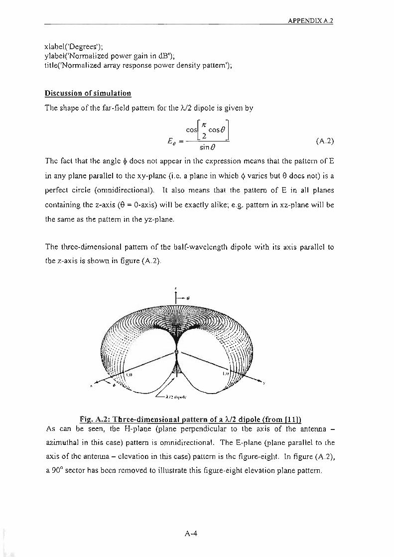
x label(,Degrees'); ylabel('Normalized power gain in dB'); title('Nomlalized array response power density pattern');
Discussion or simulation
The shape of the far-field pattern for the )../2 dipole is given by
APPENDIX A.2
(A.2)
The fact that the angle q, does not appear in the expression means that the pattern of E
in any plane parallel to the xy-plane (i.e. a plane in which q, varies but e does not) is a
perfect circle (omnidirectional). It also means that the pattern of E in all planes
containing the z-axis (9 = O-axis) will be exactly alike; e.g. pattern in xz-plane will be
the same as the pattern in the yz-plane.
The three-dimensional pattern of the half-wavelength dipole with its axis parallel to
the z-axis is shown in figure (A.2).
,
Fig. A.2: Three-dimensional pattern ora ')J2 dipole (from (11)) As can be seen, the H-plane (plane perpendicular to the axis of the antenna -
azimuthal in this case) pattern is omnidirectional. The E-plane (plane parallel to the
axis of the antenna - elevation in this case) pattern is the figure-eight. In figure (A.2),
a 90° sector has been removed to illustrate this figure-eight elevation plane pattern.
A-4

APPENDIX A.2
The array thus consists of ')../2 dipole antennas arranged coll inearly (element axes
parallel to the line of the array) on the z-axis. This collinear arrangement is very
popular amongst dipole antennas since it reduces the effect of mutual coupling
between dipole elements.
To better illustrate the pattern multiplication rule, the normalized pattern of the single
element IJ2 dipole, the array factor and the total array response are shown in figures
(A.3), (AA), (A.5) and (A.6). In each figure, the total pattern of the array is obtained
by multiplying the pattern of the single element by that of the array factor. In each
case, the pattern is normalized to its own maximum.
Figure (A.3) for N ~ 2, d ~ 0.25,1. alld beam steered to broadside (11, ~ 9(f): Since the
array factor is nearly isotropic (within 3dB), the element pattern and the total pattern
are almost identical in shape. However, the total array response is more directive
(higher gain) than the individual element. Since both the element and array factor
pattern are maximum at broadside, the total array response is also maximum at
broadside (i.e. beam steered to broadside).
Figure (AA) for N = 2, d = 0.25..1. and beam steered 10 elldfire (Bo = if): Since the
array factor is of cardioid form, its corresponding element and total patterns are
considerably different. In the total array response, the null at 90 = 0° is due to the
element pattern. Thus, even though the array factor is steered to 0°, the total response
of the array is not steered to 0°. Clearly, the element pattern prevents the total array
pattern from being steered to 0°. Therefore, the radiation pattern/characteristic of an
element can sometimes place restrictions on the scan angle of the array.
Figure (A.5) for N ~ 10, d ~ 0.25), alld beam steered to broadside (11, ~ 9(f): The
array factor and the total array response are similar to the broadside array of figure
(A.3). However, an increase in the number of elements has resulted in the presence of
sidelobes and a decrease in the main beamwidth. Thus, an increase in the number of
elements increases the main beam directivity of the array response (increase in gain
and decrease in main beamwidth). However, it also results in an increase in the
number of side lobes in the total pattern.
A-5
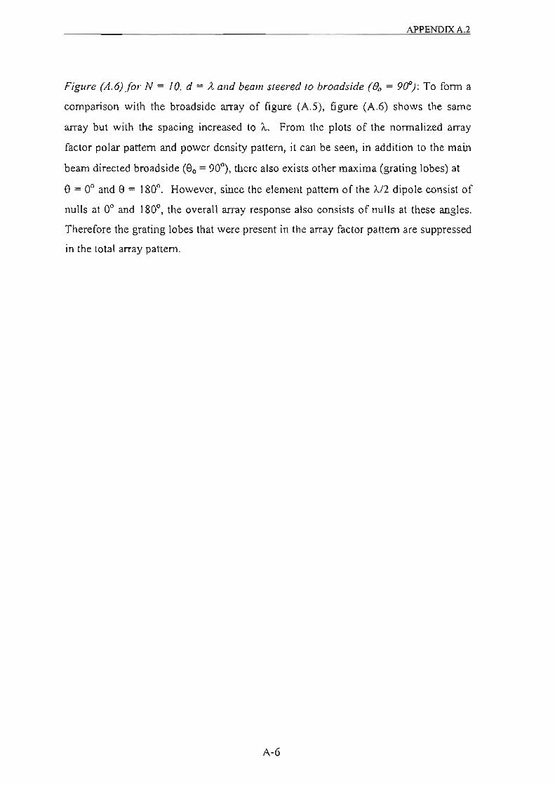
APPENDIX A.2
Figllre (A.6) Jor N ~ la. d ~ A alld beam sleered 10 broadside (0, ~ 90"): To fonn a
comparison with the broadside array of figure (A.S), figure (A.6) shows the same
array but with the spacing increased to A. From the plots of the normalized array
factor polar pattern and power density pattern, it can be seen, in addition to the main
beam directed broadside (90 = 90°), there also exists other maxima (grating lobes) at
9 = 0° and e = 180°. However, since the element pattern of the '),)2 dipole consist of
nulls at 0° and 180°, the overall array response also consists of nu lis at these angles.
Therefore the grating lobes that were present in the array factor pattern are suppressed
in the total array pattern.
A-6

Half-wa-.elergltl dipole element E-plare pattem 90,
180f---+-t-r-:;e~~E-t-t-f---~ 0
270
x -
APPEl\TOIX A.2
Polar pattem of nonnalized array factor 90,
18o'I-+l+--f-8~+-+--j+H 0
270
Total normalized array response 90,
o
270
Normalized array response power density pattem 0r-~----~~?---~~--------,
m n
•• ·5
-= -10
~ ·15 ~
ii '; -20
I ·25
Fig. A.3: Element, array factor and total arrav response for an array of collinear 1.J2 dipoles steered to broadside (N = 2, d = 0.251., 9. = 90·)
A-7
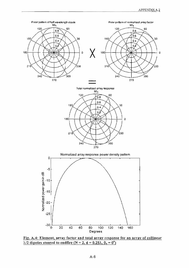
APPENDIX A.2
Polar pattern of na lf-wa~length dipole 90,
Polar pattern 01 no/lTla ~zed array factor 90,
120 60
o X 180H-+-+~+++i
270 --Total normalized array response
90, ---i'>-_ 60 120
240 ---_b_/ 300 270
240 ____ -'-_-
270
Normalized array response power density pattem Or-~--__ --~~~~--__ ~~ __ ~
'" " c
-5
:£ -10 m
'" 1-'5 ] rn -20 E :l1
-25
-30~-::::---:':--=---:7----:-:07--:-::::--:-,:-::-L:-:---.J o 20 40 60 BO 100 120 140 160 Degrees
300
o
Fig. A.4: Element, array factor and total array response for an array of collinear '1../2 dipoles steered to eodfire (N ~ 2, d ~ 0.25'1.., e. ~ 0')
A-8

APPENDIX A.2
Polar pattern of half-wavelength dipole 90,
Polar pattern of normalized array faclor 90,
ID ." C
o
·5
'c -10
·30 o
270
'20
X 'BOH-+-t--+€
Total normalized array response 90,
120 ___ -,>rr~~ 60
240
:-+-+-+----1~ 0
240 300 270
270
Normalized array response power density paHem
1\
(\ (\
/\ f\ 20 40 60 80 100 120 140 160
Oegrees
60 .B
ft-+++--1 0
300
Fig. A.S: Element, array factor aDd total arrav response for an array of collinear ),)2 dipoles steered to broadside (N ~ 10, d ~ 0.251,., e, ~90')
A·9
., m " -10 = o .~
"i -15 ~
I ·lD
Polar pattem of half-wavelenglh dipole 90,
270
x 30
APPENDIXA.2
Polar pattem of ntllmilbed array factor 90,
3-+++-1 0
Total norrnaiiZed" array response 90,
'20 60
'.0f-+-+-t---f :a-+++-j 0
270
PIoI ollhe nonnalized arrlyfactOf power density Notrmll zed array response power density pattem
.,
'"O~-'2~0'-~,mO~~6~O~~~"-"~OO~~'2~O~~"~Or"~'60",~ Degrees
~OOW--'2~0"-~~~~60~~8~0--"OO~JY'2~O~~"~O~t'60or-" Degrees
Fig. A.6: Element, array factor and total array response for an array of collinear ').)2 dipoles steered to broadside (N - 10, d - A., 90 - 90°)
A- I Q

APPENDIX A.3
A.3 LNA design
A.3.1 Active device selection
The gallium arsenide field-effect transistor (GaAs FET) and the bipolar junction
transistor (BJT) are the two most commonly used devices in the design of amplifiers.
BJTs used in UHF and microwaves are usually of planar npn si licon type. The
advantages of si licon planar BJTs over other types of transistors at high frequencies
are that they represent mature technology both in the understanding of physics and the
device design, low cost and proven reliabil ity_ Compared with its microwave B1T
counterpart, the GaAs FET has high gai n and lower noise figure and can operate at a
higher maximum frequency. The difference in frequency handling capacity between
BITs and GaAs FETs is due to the slower minority carriers in the base region of the
BJT whereas conduction in a GaAs FET depends mainly on majority carriers.
The ATF-IOI36 GaAs FET was selected on the basis of the description of the device
by the manufacturer as being suitable for use in low noise amplifier applications in the
0.5 to J 2GHz range. It was also selected on the basis of availability and cost
effectiveness.
A criterion to check whether a single stage amplifier will suffice is to check that the
device has a maximum available gain, MAG (in the case of an unconditionally stable
device) greater than the specified gain at the frequency of interest. In the case of a
potentially unstable device, a single stage wi ll suffice when the maximum stable gain
(MSG) greater than the specified gain at the frequency of interest. The speci fied
minimum gain is lOdB, so the device must have a MAG or MSG greater than IOdB at
2GHz for a single stage to suffice. The S parameters of the device at Vos = 2V and
IDs = 25mA are given in the manufacturer 's data sheet and partially reproduced in
table (A. I ) below.
Freq. 8" 8" 8" 8" (GHz) M.g. Angle M.g. Angle Mag. Angle Mag. Angle
2 0.79 -66 4.64 113 0.074 59 0.30 -31
. Table A.!. 8 parameters of ATF-10136 G.As FET at VDs 2V and Ios 25mA
A-l1
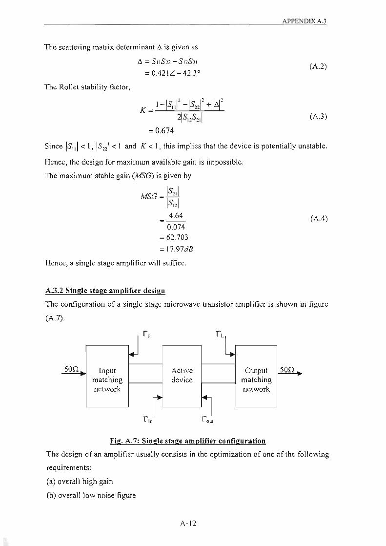
The scattering matrix determinant 6. is given as
The Rollet stability factor,
6. = S 1IS22 - S l2S 21
= OA2lL - 42.3°
= 0.674
APPENDIX A.3
CA.2)
CA.3)
Since ISI II < 1, IS22 I < 1 and K < 1 , this implies that the device is potentially unstable.
Hence, the design for maximum available gain is impossible.
The maximum stable gain (MSG) is given by
MSG = is,,i is,,i 4.64
0.074 = 62.703
= l7 .97dB
Hence, a single stage amplifier will suffice.
A.3.2 Single stage amplifier design
CAA)
The configuration of a single stage microwave transistor amplifier is shown in figure
CA. 7).
,
t .-r
50n Input Active Output 50n . matching device matching network network ... .-
Fig. A.7: Single st;lge amplifier configuration
The design of an amplifier usually consists in the optimization of one of the following
requirements:
Ca) overall high gain
Cb) overall low noise figure
A-12
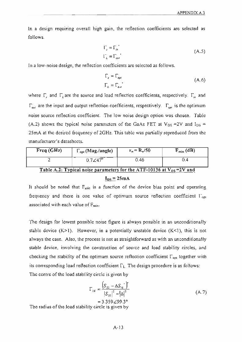
APPENDIX A.3
In a design requtnng overall high gain, the reflection coefficients are selected as
follows.
rJ =f;,, '
rL = f " ... ,·
In a low·noise design, the reflection coefficients are selected as follows.
r J = r op,
r L =f"~l '
(A.5)
(A.6)
where f J and fL are the source and load reflection coefficients, respectively. fi~ and
f o ... , are the input and output reflection coefficients, respectively. f op, is the optimum
noise source reflection coefficient. The low noise design option was chosen. Table
(A.2) shows the typical noise parameters of the GaAs FET at Vos =2V and IDs =
25mA at the desired frequency of 20Hz. This table was partially reproduced from the
manufacturer's datasheets.
Freq (GHz) r,p. (Mag./angle) r,- R,/50 Fm;, (dB)
2 0.7L47" 0.46 0.4
. Table A.2: Typical noISe parameters fo r tbe ATF-IO I36 at VDs - 2V and
]os= 2SmA
It should be noted that Fmin IS a function of the device bias point and operating
frequency and there is one value of optimum source reflection coefficient r opt
associated with each value ofFmin.
The design for lowest possible noise figure is always possible in an unconditionally
stable device (K>l). However, in a potentially unstable device (K< l), this is not
always the case. Also, the process is not as straightfoTWard as with an unconditionally
stable device, involving the construction of source and load stability circles, and
checking the stability of the optimum source reflection coefficient f opt together with
its corresponding load reflection coefficient r L. The design procedure is as follows:
The centre of the load stability circle is given by
r = (S22 -ASu ' r " IS"I' -1"'1' (A.7)
= 3.359L99.3' The radius of the load stability circle is given by
A-13

IS I2S" I
R 2S = ,,---'IIS ,--7,1' --"--1"''"'''1' I
= 3.951 The centre of the source stability circle is given by
r _(SI I- l1Sn 'Y ,,- Is" I'-I"'I'
= 1.620L74.2' The radius of the source stability circle is given by
ISI2 S,,1 R = ,--'--,;,-= :-;
" IIS"I' -1"'1 '1 = 0.768
APPENDIX A.3
(A .8)
(A.9)
(A.IO)
The source and load stability circles are plotted on the Smith chart shown overleaf. A
nonnalized impedance of 1 corresponds to 81 .5mm. Since ISII I and IS221 are less
than I at 2GHz, the Smith chart represents a stable operating point for both source and
load tenninations i.e. the stable regions are outside the stability circles. However,
since the load stability circle encloses (encompasses) the centre of the Smith chart, all
areas inside the load stability circle are stable for load temlinations i.e. the areas
outside the load stability circle are unstable load tenninations. To check whether a
minimum noise figure of Fmin = OAdB (@ 2GHz) is achievable with a potentially
unstable device, it is necessary to ensure that r s = r Opt lies in the stable region of the
source stability circle plot. If this is not the case, then a value other than r opt must be
chosen for the source reflection coefficient 1 $, at the expense of having a noise figure
higher than Fmin . After selecting l S, whether it is equal to l opt or not, conjugate
matching is normally employed on the output of the device i.e. the load reflection
coefficient is made equal to the complex conjugate of the output reflection coefficient.
The computed value of 1 L must of course lie within the stable region of the load
stability plot.
The value of ls = r opt = 0.7 L47° (corresponding to Fmin = O.4dB) is plotted on the
Smith chart. It lies within the stable region of the source stability circle. The
corresponding value of load reflection coefficient r L is computed as
A-14

.. "'. _ 1(10).,, .. .. .... ~~ - 0 .. " " '\..q;,;~ ., ,, -~ ". ,,' ". '" ". '" '- •• ," .. , " M '" "
., . " . • ORIClN
, '"
The Complete Smith Chart Black Magic Design
MDlALLY SCALm rAlUYotnDS
TOWAlDLOAD _ >
" .. .. .. " " ,
" .. , • • ,
" " " " " '" " " " l" _ O .. '" .. ,,, ". ,,' ". - ~, ,,' " ,., " " " " ," ". '" ",l .. . " ' . •• '" ..
• , ~
'" ". ,,' .. "' " " " "
.,~ <_ rowA~DCENUATOIt 4:-t':. , , .. "
, '" .. - ~t>~ " , , \"'~ , " " " <r~# ;t
" !.I'U " .- <"'cl' "' ". "' ... ., " .. "
" .. " " , " /'

APPENDIX A.3
r, = (S" -Llr", J. l - r "" S" (A. 1 1)
= 0.265L - 84.9· This is now plotted on the Smith chart. It lies within the stable region of the load
stability circle. Since both r L and rOp! lie in the stable region of the load and source
stability circles, it is possible to design for minimum noise figure ofOAdB.
The transducer power gain OT for this minimum noise figure can now be calculated as
_ IS,.I'(1- lrJ X1- lr,I') Or - 2 11- SlI r s - rLsn + 6rL r sl
= 33.319 (A.12)
= 1 S.S23dB
A.3.3 Topology
One of the most important aspects of high-frequency circuit design and microwave
engineering is the problem of impedance matching. Impedance matching is the
design of a circuit to be inserted between a source and load (both used in the general
sense) so as to provide maximum power transfer between them. One of the most
fundamental criteria is that a matching network must at least be theoretically lossless.
The reason is obvious. As a consequence. matching networks in high-frequency
circuit design always take the form of a Le (never R) circuit in the discrete case. or in
the form of transmission line sections and stubs in the distributed case.
The bandwidth specification is 2::10MHz at a centre frequency of2GHz. This gives a
Q factor of:
Q '" f · Llf
2GHz '" ") O='M":::H:-z
'" 200
(A.13)
The Q factor is a useful measure of the bandwidth performance of a filter/amplifier
[18]. With a Q factor less than 10. the device is classi tied as wideband whereas with a
Q factor greater than 10. the device is classified as narrowband. In wireless
communicat ions, higher frequency bands are being sought to avoid congestion. As a
result, wider bandwidth amplification would be required. There are a number of
A·1S

APPENDIX A.3
techniques used to maximize the bandwidth of an amplifier [65]. One technique is the
employment of wideband matching.
Wideband matching can be accomplished by means of multi section quarter
wavelength transfonner matching networks. Multisection transfonner matching
offers increased bandwidth at the expense of having a large number of ')J4 sections.
Depending on the frequency of operation, substrate permittivity and thickness, this
can lead to impractical circuit sizes. In a multi-stage amplifier, the use of multi section
Al4 transfonners (2 or more sections) results in a circuit that is considerably much
larger than with its single section counterpart (for the same substrate and frequency of
operation). Hence single section 1J4 matching networks were chosen because of its
practicality.
A quarter-wavelength transfonner can only be used to match a purely resistive source
to a purely resistive load. However, should eitherlboth the source or load be complex,
it is necessary to first cancel the reactive component(s) before using a quarter
wavelength transfomler. Cancellation of the reactive components can be achieved in
two ways:
(a) By insertion of a length of transmission line (of arbitrary characteri stic impedance)
in series with the source andlo r load so that the impedance seen at the input of the
length of transmission line is purely resistive. The length of the transmission line is
determined by using a Smith chart. It should be noted that the precision obtainable
from the chart is not very good.
(b) By insertion of a stub in parallel wi th the complex source and/or load. The stub
cancels the susceptance of the source andlor load impedance so that the impedance
seen at the input of the stub is purely resistive. The stub can take the form of an open
circuit or short-circuit length of transmission line in parallel with the source and/or
load. Good short-circuit stubs are difficult to implement and realize in microstrip as it
requires the use of through-hole plating which is costly. Also in some instances the
stubs are so thin (large characteristic impedance) that they require precision drilling
equipment (ultrasonic drill and small diameter bits) to prevent cracking of the
substrate. Therefore short-circuit stub implementation requ ires skill . Hence the use
of short-ci rcuit stubs is discouraged.
A-J6
APPENDIX A.3
Hence, single section quarter-wavelength transformers with open-circuit stubs as
matching networks were only considered in this design. The choice of substrate is
important in the design of microstrip circuitry. Circuit performance can be degraded
by the choice of a poor substrate. Electrical, mechanical and thermal stability
properties should be considered when choosing a substrate. However, in spite of its
lossyness, PCS was used in this design due to its avai lability and cost-effectiveness.
The main specifications of the pes substrate are listed in table (A.3) below.
Dielectric constant Er 4.1 ± 0.2
Dielectric thickness d 0.9mm .
Table A.3 : pe R malO specificatIOns The relatively low value of the dielectric constant coupled with the relatively low
frequency of operation (lower end of microwave frequency band) allows for easy
etching of the circuit. Thus there is no need for ultra-precision etching faci li ties that
would otherwise be required in the case of a high dielectric constant (for the same
dielectric thickness and frequency of operation).
A.3.3.1 Input matching
Input matching is required to match the 500: source to Zop,- where Zop,- is given by
.2.(I+r.,:) 2 = --"-'--";'--' opf J-r . . ,.
= 106.864L - 63.5' (A.14)
= 47.65 - )9S.65Q The - j95.6SO: reactive component of ZoPI- can be cancelled with a parallel (shunt)
reactance to ground. The admittance YOpl- is given by
y • = _ 1_ opf Z.
." = 0.0041721 + )0.0083761
(A.IS)
The +jO.0083761 susceptance needs to be cancelled with a susceptance value of
-jO.0083761 in parallel. To realize this susceptance, we note that an open-circuited
stub is seen to have an input admittance of
(A. 16)
where Yo is the characteristic admittance and B = 2Jd / A. . If B = 37t14 i.e. 1= 31J8,
then Y = :JY •. Thus an open-circuited stub that is three.eights of a wavelength long
looks like a shunt element with admittance -jYo' In this case, Y = -jYo = -jO.008376I
A-17
APPENDIX A.3
and thus Yo = 0.00S3761 or the characteristic impedance of the open-circuited stub is
given by Z, ~ 1 /Y,~ 11 9.387>1.
Since the source generator is 50n and in order to realize the parallel conductance
element of 0.004 1721 S, a quarter-wave transformer (l = ),)4) of impedance
is employed.
Z, ~~Z,ZL .-------,--
~ 50---'--0.0041721
~ 109.4730
A.3.3.1.1 Microstrip implementation
fa> Calculation ofIine widths
(A.17)
Bahl and Trivedi [89] have proposed two formulae to calculate line widths (w). given
substrate thickness (d) and line impedance (20):
w SeA ~
w for - (2
d
h A z'NI·+I &.- 1[023 0.11] were = - --+-- . +-602 E,+ 1 E,
and
w ~~[B - I -ln(2B- I)+ 8.- I{ln(B_I)+0.39_ 0.61}] d 7f 2E, E,
3777r where B = ~
220"l/c,
son input line width
using equation (A.19): ~ = 2.01630283 or w = 1.815mm cl
109.473n quarter-wave section line width
using equation (A. IS): w = 0.3730937 or W= 0.336mm d
A-18
w for - )2
d
(A.18)
(A.19)
119.3870 open-circuit stub width
using equation (A.18): w ~ 0.286058 1 or w ~ 0.257111111 d
(b) Calculation of line lengths
APPENDIX A.3
Two parameters that are of importance in the calculation of rnicrostrip line lengths are
the effective dielectric constant (~) and the guided wavelength (Ag). These are given
respectively, by:
& + 1 £ - 1 8 , ~ -'-2 - + '2 -J-;=~~d~
1+ 12 -w
and
A ~~ 'F.
c 3xlO8ms- 1
where A" = - = 9 = 150mm f 2x l0 Hz
son input line length
The 50n input line length was chosen to be /...g /4 .
using equation (A.20): S. ~ 3.1378856
using equation (A.21): Ag ~ 84.678mm
:. length of 50n line is 21.17mm
109.473Q quarter-wave section line length
using equation (A.20): S. ~ 1.724
using equation (A.21): A, = 89.337mm
I ~ ,,/ 4 ~ 22.334mm
119.3870 open-circuit stub length
using equation (A.20): S. ~ 2.7865117
using equation (A.21): A, ~ 89.859mm
1= 3,,/8 ~ 33.697mm
A-19
(A.20)
(A.21)

APPENDIX AJ
Figure (A.8) shows the microstrip input matching network (dimensions In
millimetres).
21 17 2233
J:. T
33.69
--.j~ 0.257
Fig. A.S: Microstrip input matching network
A.3.3.2 Output matchine:
0.336
Output matching is required to match the output of the amplifier to the son load i.e.
ZL" to 50n.
= 52.263L29.6° (A.22)
= 45.434 + j25.829n
where r L" is computed as 0.265L84.9° from equation (8.10).
The +j25.829n reactive component of ZL' can be cancelled with a shunt reactance to
ground. The admittance YL" = 1/2L* = 0.0 166338 - jO.0094562. The -jO.0094562
susceptance needs to be cancelled with a susceptance value of +jO.0094562 in
parallel. Using the same procedure as the input matching network, the open-circuited
stub should be one-eight of a wavelength long (B = 7tf4) with a characteristic
impedance of 2,= IIY, = 1/0.0094562 = 105. 75 1n.
With the reactive component of ZL· cancelled, a quarter wavelength transfonner can
now be used to match the parallel conductance element of 0.0166338S to the son load. The characteristic impedance of the IJ4 transformer is
A-20

zo~~z,z, r---:---
I 50 = 0.0166338
= 54.826n
A.3.3.2.1 Microstrip implementation
(a) Calculation of line widths
105.7510 open-circuit stub width
using equation (A.18): w = 0.4123408 or w = 0.371111111 d
54.826Q quarter-wave section line width
. . ( ) W 6 uSing equatIOn A.I8 : - = 1. 72723 3 or w = 1.555mm d
son output line width
using equation (A.19): w = 2.01630283 or w = 1.815mm d
(h) Calculation of line lengths
IOS.7Sln open-circuit stub length
using equation (A.20): £.,~ 2.8325095
using equation (A.2 1): .<,.= 89.126mm
1= Ag/8 ~ 11.141mm
54.826n quarter-wave section line length
using equation (A.20): t:" = 3.0998143
using equation (A.21): AB ~ 85. 197mm
1 = Ag/4 = 21.299mm
son output line length
APPENDIX A.3
(A.23)
The 50n output line length was chosen to be I..g/4 (same length as 50n input line).
using equation (A.20): £., ~ 3. 1378856
using equation (A.21): AB ~ 84.678mm
:. length of 50n line is 21.17mm
A-2 1

APPENDIX A.3
Figure (A.9) shows the microstrip output matching network (dimensions In
mill imetres).
1.555-.:l I" 21.29 .1" 21.17 .1
TILlI ~ __ ~ ___ III.815
-+11+-0.371
Fig. A.9 : Microstrip output matchine: network
A.3.4 Bias circuit
It has been said that the least considered factor in microwave transistor amplifier
design is the bias network [90]. While considerable effort is spent in designing for a
given gain, noise figure and bandwidth, linIe effort is spent in the dc bias network.
The cost per decibel of microwave power gain or noise figure is high, and the
designer cannot sacrifice the amplifier perfonnance by having a poor dc bias design.
The purpose of a good dc bias design is to select the proper quiescent point and hold
the quiescent point constant over variations in transistor parameters and temperature.
A resistor bias network can be used with good results over moderate temperature
changes. However, an active bias network is usually preferred for large temperature
changes.
GaAs FETs can be biased in several ways. One common bias circuit used for low
noise, high gain, high power and high efficiency is shown in figure (A. 1 0).
A-22

APPENDIX A.3
Co - OUT ( • Co
. ~ ATF10136 IN -If • I,
1 RFC
RFe
lCb
i Cb c.::;' +Vd -
Fig. A.l0: Bias circuit
Low noise amplifiers operate at relatively low drain-source voltage Vos and current
lDs, usually los = 0.1510ss (loss is the drain-source current when VGS = 0). This
configuration gives the lowest source inductance and hence lowest noise figure and
higher gain. Most high-frequency amplifier circuit designs for high gain or low noise
figure requires that the source lead be dc grounded as close to the package as possible
so that the source series feedback is kept to an absolute minimum. However, ID
becomes sensitive to variations in temperature and loss.
The above bias circuit reqUires a bipolar power supply i.e. one positive and one
negative supply. The proper turn-on sequence must be applied to prevent transient
burnout of the GaAs FET device. If the drain is biased positive before the gate, the
device will operate momentarily beyond its safe operating region. Therefore, the
proper turn-on sequence is: first apply a negative bias to the gate (VG < 0) and then
apply the drain voltage (VD > 0). One method to accomplish the previous turn-on
procedure is to turn both power supplies at the same time and to include a long RC
time constant in the VD supply and a short RC time constant network in the negative
supply VG-
A bipolar power supply incorporating the above turn-on sequence is available in the
Programme of Electronic Engineering. This is shown in figure (A.It).
A-23

APPENDIX A.3
Fig. A.II: Power supplv available in tbe Programme of Electronic Engineering
for the biasing of GaAs FET amplifiers
RF chokes and decoupling (bypass) capacitors (Cs) are used to isolate RF from the
DC power supply. Typical values for the chip bypass capacitors are 50pF to 50OpF.
The RF choke should have a reactance of at least five times the impedance of the
circuit at the point where the choke is to be connected. Chip coupling capacitors (Cc)
are used to AC couple the input and output of the amplifier. Typical values for the
coupling capacitors are 100pF to 1000pF, high Q capacitors. They are also chosen to
have low loss at the frequency of interest and low impedance compared to 500.. For
this design, coupling and bypass capacitors (0805 size) of value IOnF were chosen.
Their impedance Xc at 2GHz is
X =_1_ , 21IfC
I = -----,C---cc
2Jr x 2 X 109 X 10 xl 0-9
= 7.958x 1O-' n
(A.24)
As can be seen that this impedance is negligible when compared to the 500. system
characteristic impedance.
The bias conditions of the ATFI0136 is Vos = 2V and Ios = 25mA. From the
datasheet, the value of I DSS and Vp (pinchoff voltage) are obtained as 130mA and
-1.3V, respectively. The gate voltage can be calculated using the following fomlUla:
10,=1=(1-:' )' Solving for Vg" yields Vg, = -1.87V or -O.73V. Choosing I Vg, I < I Vp I :::::) Vgs = -O.73V. Since the source is grounded, Vg= Vgs = -0.73V.
A-24
(A.25)

APPENDlXA.4
A.4 ADS simulation issues
This section provides a detailed description on some ofthe different issues that had to
be considered to enable the simulations in this thesis to run successfully. These issues
arose from the BER simulations in chapter 5 and 6.
A.4.! BER simulation setup
As mentioned in chapter 5, the Improved Importance Sampling (liS) BER
measurement technique was used instead of the Monte Carlo technique because it
requires a rewer number of bits to be simulated thereby reducing the simulation run
time considerably. Figure (A.12) shows the liS BER ADS sink that was used.
=,::.:,b e S '" ,,,
" 5\ort",or_Volue T ;m .. l)n, I_or _vcl ,.
5ymbO IT ;me- I 0 Numthreshol d_1 Oe1oyBovnd"'-1 0 berOutput=ber only NBw_3 0 Hz SyS I emType:PAt.! [~;;tVo'-O 1 EsOverNo-3 0
Fig. A.12: Improved Importance Sampling (lIS) HER sink used in ADS
As can be seen from figure (A. 12), this block has (among other input fields) , an input
field for the E,jNo value where Eb is the energy per bit and No is the one-sided power
spectral density of bandlimited white noise. However, in the existing simulation
setup, the user has no prior knowledge of this value. However, there are two methods
to determine this value
(i) Calculation
(ii) Using the Monte Carlo BER measurement sink
(i) C alculation
The following formulae are used in ADS for the calculation of Eb and No:
(A.26)
where P ESREF = source power in the reference RF signal at output of the IF
amplifier (see figure (5.3) in chapter 5), Tb ~ bit time.
(A.27)
A·25
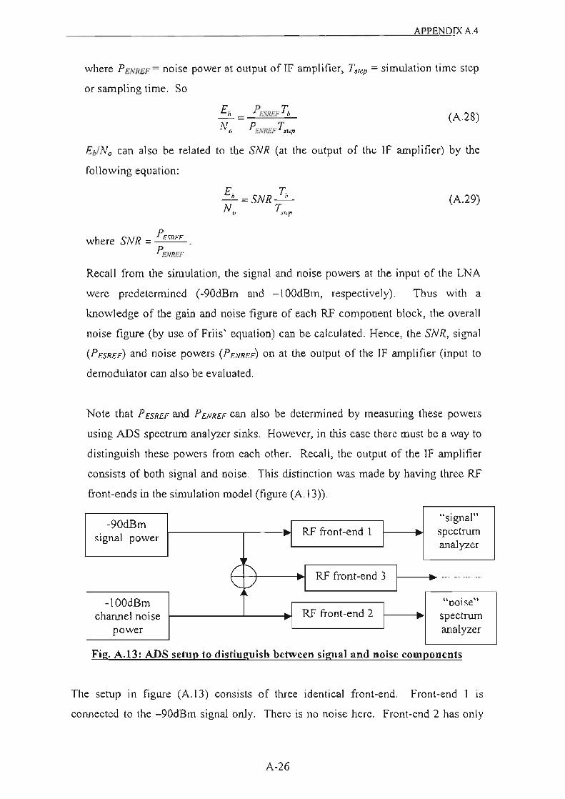
APPENDIX A.4
where P ENREF= noise power at output of IF amplifier, T s,ep = simulation time step
or sampling time. So
(A.28)
E"JN. can also be related to the SNR (at the output of the IF amplifier) by the
following equation:
where SN R = P ESREF •
PENREF
(A.29)
Recall from the simulation, the signal and noise powers at the input of the LNA
were predetermined (-90dBrn and - IOOdBm, respectively). Thus with a
knowledge of the gain and noise figure of each RF component block, the overall
noise figure (by use of Friis' equation) can be calculated. Hence, the SNR, signal
(PESREF) and noise powers ( P ENREF) on at the output of the IF amplifier (input to
demodulator can also be evaluated.
Note that P ESREF and P ENR£F can also be determined by measuring these powers
using ADS spectrum analyzer sinks. However, in this case there must be a way to
distinguish these powers from each other. Recall, the output of the IF amplifier
consists of both signal and noise. This distinction was made by having three RF
front-ends in the simulation model (figure (A. 13)).
-90dBm "signal"
signal power RF front-end I spectrum analyzer
r '\ RF front -end 3 i "I ...... ............. _ .....
\.... ,-/ -IOOdBm " noise"
channel no ise RF front -end 2 spectrum power analyzer
Fig. A.13: ADS setup to distinguish between signal and noise components
The setup in figure (A.13) consists of three identical front-end. Front-end 1 is
connected to the - 90dBrn signal only. There is no noise here. Front-end 2 has only
A-26

APPENDIXA4
noise power while front-end 3 has a combination of both noise and signal power.
Front-end 3 is the actual receiver used to perform demodulation, despreading and
BER measurements. Now that the noise and signal components can be distinguished
individually, their spectrums can be integrated to find their respective powers. This is
achieved using the specyower function in ADS. The ADS documentation has more
infomlation on this.
(ii) Using the Monte Carlo HER measurement sink
Figure (A.14) shows this sink.
. ~ .. .. ~~"bt r ,-~ , .. W .- ' ..
berM('4 b1 Stort=OF_Volue Stop=OF_Vo I ue TimeUn, t-OF _ Vu UI:'
Symbo IT ime= 1 0 NumThresholdo::=l De I oyBound=-l .0 berOutput ber only
Fig. A.14: Monte Carlo HER measurement sink used in ADS
Notice that this sink has inputs for both signal (PESREF) and noise (PENREF)
components. This implies that these must be distinguishable in the simulation setup.
The setup of figure (A.13) could be used to differentiate between the signal and noise
components. However, with this method, the Monte Carlo sink computes the Et/No
value (using equations (A.26), (A.27) and (A.28» as part of the BER measurement.
Thus it is unnecessary to have spectrum analyzer sinks and write funct ions for
calculating the spectrum powers. Also, the Et/No value is independent of the number
of samples.
In the simulation setup, both methods (described above) were used to veri fy and
correlate the Et/No value.
A-27

APPENDIX AA
A.4.2 Scaling of Et/No
As mentioned in chapter 5, the E,fNa values were scaled by a factor 6 (7.782dB) prior
to be used as an input to the lIS BER sink. The reasons for this are as fo llows: From
equations (A.28) and (A.29) it should be noticed that E,IN. is a function of the
simulation time step (Tslep). However, in CDMA, the processing gain Gp is related to
the E,IN. by the fo llowing equation [57]:
E, =SNRxG N ' •
(A.30)
On comparison of equation (A.29) with equation (A.30). it is appropriate that EtlNo to
be consistent with the standard defi nition of Et/No in tenns of the processing gain
[57]. With a chip rate (4.096MHz) of 42 times the data (bit) rate (Gp = 42) and a
simulation sampling rate of 6 times the chip rate, the scaling factor K is computed as
1: G =-'-xK=42
P T.,.,p
42
4.096MHz I
6x 4.096MHz
xK =42
=:> K =.!. = -7.782dB 6
Thus the EtlNo values (obtained by the methods described earlier) had to be reduced
by 7.782dB prior to input of the lIS BER measurement sink. This effectively reduces
the simulation bandwidth from 24.576MHz (l ITstep) to a spread bandwidth of
4.096MHz. This 4.096MHz bandwidth is used as the noise bandwidth (NBw) input
field in the lIS BER sink.
A.4.3 BER curve irregularities
It can be noticed that the BER plots in chapter 5 are not smooth i.e. they do not have
the expected "waterfall" BER appearance. Instead there are "flat areas" on these
curves. An attempt to find the cause of this irregularity has been unsuccessful. These
" nat areas" occur for a fixed range of EtlNo or (SNR). They also occur for both the ns and Monte Carlo BER measurement techniques. This irregularity may be due a
software bug. A response from Agilent Technologies' product technical support
division, on this phenomenon, is still awaited.
A-28