Embed Size (px)
Citation preview
Design Constraints for Libero SoC v11.8 User Guide
NOTE: PDF files are intended to be viewed on the printed page; links and cross-references in this PDF file may point to external files and generate an error when clicked. View the online help included with software to enable all linked content.

Design Constraints for Libero SoC v11.8 User Guide
3
Microsemi makes no warranty, representation, or guarantee regarding the information contained herein or the suitability of its products and services for any particular purpose, nor does Microsemi assume any liability whatsoever arising out of the application or use of any product or circuit. The products sold hereunder and any other products sold by Microsemi have been subject to limited testing and should not be used in conjunction with mission-critical equipment or applications. Any performance specifications are believed to be reliable but are not verified, and Buyer must conduct and complete all performance and other testing of the products, alone and together with, or installed in, any end-products. Buyer shall not rely on any data and performance specifications or parameters provided by Microsemi. It is the Buyer’s responsibility to independently determine suitability of any products and to test and verify the same. The information provided by Microsemi hereunder is provided “as is, where is” and with all faults, and the entire risk associated with such information is entirely with the Buyer. Microsemi does not grant, explicitly or implicitly, to any party any patent rights, licenses, or any other IP rights, whether with regard to such information itself or anything described by such information. Information provided in this document is proprietary to Microsemi, and Microsemi reserves the right to make any changes to the information in this document or to any products and services at any time without notice.
About Microsemi
Microsemi Corporation (Nasdaq: MSCC) offers a comprehensive portfolio of semiconductor and system solutions for aerospace & defense, communications, data center and industrial markets. Products include high-performance and radiation-hardened analog mixed-signal integrated circuits, FPGAs, SoCs and ASICs; power management products; timing and synchronization devices and precise time solutions, setting the world's standard for time; voice processing devices; RF solutions; discrete components; enterprise storage and communication solutions; security technologies and scalable anti-tamper products; Ethernet solutions; Power-over-Ethernet ICs and midspans; as well as custom design capabilities and services. Microsemi is headquartered in Aliso Viejo, California, and has approximately 4,800 employees globally. Learn more at www.microsemi.com.
5-02-00046-25/01.17
Microsemi Corporate Headquarters One Enterprise, Aliso Viejo, CA 92656 USA Within the USA: +1 (800) 713-4113 Outside the USA: +1 (949) 380-6100 Fax: +1 (949) 215-4996 Email: [email protected] www.microsemi.com
©2017 Microsemi Corporation. All rights reserved. Microsemi and the Microsemi logo are registered trademarks of Microsemi Corporation. All other trademarks and service marks are the property of their respective owners.
Design Constraints for Libero SoC v11.8 User Guide
4
Table of Contents Table of Contents ..................................................................................................................................... 3
Design Constraints .......................................................................................................7
Families Supported ......................................................................................................9 Constraint Entry ..................................................................................................................................... 12 Constraint File Format by Family .......................................................................................................... 15
Basic Concepts ............................................................................................................16 Region .................................................................................................................................................... 18 Location ................................................................................................................................................. 19
I/O Attributes .............................................................................................................20 Bank Name............................................................................................................................................. 22 User Reserved ........................................................................................................................................ 40 I/O Bank Settings Dialog Box (IGLOO and ProASIC3 only) ............................................................... 42 I/O Bank Settings Dialog Box................................................................................................................ 43
Entering Constraints .................................................................................................45 Importing Constraint Files ..................................................................................................................... 46
Exporting Constraint Files ........................................................................................48
Constraints by Name: Timing...................................................................................49 Create Generated Clock ......................................................................................................................... 50 Set Clock Latency .................................................................................................................................. 52 Set False Path ......................................................................................................................................... 55 Set Input Delay ...................................................................................................................................... 56 Set Load on Output Port ......................................................................................................................... 57 Set Maximum Delay .............................................................................................................................. 58 Set Minimum Delay ............................................................................................................................... 59 Set Multicycle Path ................................................................................................................................ 60 Set Output Delay .................................................................................................................................... 61
Constraints by Name: Physical .................................................................................62
Assign I/O to Pin ........................................................................................................63 Assign I/O Macro to Location................................................................................................................ 64 Assign Macro to Region ........................................................................................................................ 65 Assign Net to Global Clock ................................................................................................................... 66 Assign Net to Local Clock ..................................................................................................................... 67 Assign Net to Quadrant Clock ............................................................................................................... 68 Assign Net to Region ............................................................................................................................. 69 Create Region ......................................................................................................................................... 71 Delete Regions ....................................................................................................................................... 72 Move Block ............................................................................................................................................ 73
Design Constraints for Libero SoC v11.8 User Guide
5
Move Region .......................................................................................................................................... 74 Reserve Pins ........................................................................................................................................... 75 Reset Attributes on an I/O to Default Settings ....................................................................................... 76 Reset an I/O Bank to Default Settings ................................................................................................... 77 Reset Net's Criticality to Default Level ................................................................................................. 78 Set Block Options .................................................................................................................................. 79 Set Net's Criticality ................................................................................................................................ 80 Set Port Block ........................................................................................................................................ 81 Unassign Macro from Region ................................................................................................................ 82 Unassign Macro(s) Driven by Net from Region .................................................................................... 83 Unreserve Pins ....................................................................................................................................... 84
Constraints by Name: Netlist Optimization ............................................................85 Demote Global Net to Regular Net ........................................................................................................ 86 Promote Regular Net to Global Net ....................................................................................................... 87 Restore Buffer Tree ................................................................................................................................ 88 Set Preserve ............................................................................................................................................ 89
Constraints by File Format - SDC Command Reference .......................................90 SDC Syntax Conventions ....................................................................................................................... 91
Referenced Topics ......................................................................................................93 set_false_path ....................................................................................................................................... 103 set_input_delay .................................................................................................................................... 104 set_max_delay (SDC) .......................................................................................................................... 106 set_output_delay .................................................................................................................................. 110
Design Object Access Commands...........................................................................112 all_inputs .............................................................................................................................................. 113 all_outputs ............................................................................................................................................ 114 all_registers .......................................................................................................................................... 115 get_cells ............................................................................................................................................... 116 get_clocks ............................................................................................................................................ 117 get_pins ................................................................................................................................................ 118 get_nets ................................................................................................................................................ 119 get_ports ............................................................................................................................................... 120 About Physical Design Constraint (PDC) Files ................................................................................... 121 PDC Syntax Conventions ..................................................................................................................... 123 PDC Naming Conventions ................................................................................................................... 125 assign_global_clock ............................................................................................................................. 127 assign_local_clock ............................................................................................................................... 128 assign_net_macros ............................................................................................................................... 130 assign_quadrant_clock ......................................................................................................................... 132 assign_region ....................................................................................................................................... 134 define_region ....................................................................................................................................... 135 delete_buffer_tree ................................................................................................................................ 138 dont_touch_buffer_tree ........................................................................................................................ 139
Design Constraints for Libero SoC v11.8 User Guide
6
move_block .......................................................................................................................................... 140 move_region ........................................................................................................................................ 142 reserve .................................................................................................................................................. 143 reset_floorplan ..................................................................................................................................... 144 reset_io ................................................................................................................................................. 145 reset_net_critical .................................................................................................................................. 147 set_block_options................................................................................................................................. 148 set_multitile_location ........................................................................................................................... 171 set_net_critical ..................................................................................................................................... 174 set_port_block ...................................................................................................................................... 175 set_preserve .......................................................................................................................................... 176 unassign_global_clock ......................................................................................................................... 177 unassign_local_clock ........................................................................................................................... 178 unassign_macro_from_region .............................................................................................................. 179 unassign_net_macros ........................................................................................................................... 180 unassign_quadrant_clock ..................................................................................................................... 181 undefine_region ................................................................................................................................... 182 unreserve .............................................................................................................................................. 183
I/O Standards ..........................................................................................................184

Design Constraints for Libero SoC v11.8 User Guide
Design Constraints
Design constraints are usually either requirements or properties in your design. You use constraints to ensure that your design meets its performance goals and pin assignment requirements. The Libero SoC software supports both SDC timing and PDC physical constraints. In addition, it supports netlist optimization constraints. You can set constraints by either using Microsemi's interactive tools (I/O Editor, Chip Planner, and Constraint Editor) or by importing constraint files directly into your design session. With Enhanced Constraints Flow, use the Constraint Manager to manage all your design constraints.
SDC Timing Constraints Timing constraints represent the performance goals for your designs. Microsemi software uses timing constraints to guide the timing-driven optimization tools in order to meet these goals. You can set timing constraints either globally or to a specific set of paths in your design. You can apply timing constraints to:
• Specify the required minimum speed of a clock domain • Set the input and output port timing information • Define the maximum delay for a specific path • Identify paths that are considered false and excluded from the analysis • Identify paths that require more than one clock cycle to propagate the data • Provide the external load at a specific port
To get the most effective results from the Designer software, you need to set the timing constraints close to your design goals. Sometimes slightly tightening the timing constraint helps the optimization process to meet the original specifications.
PDC Physical Constraints Designer software enables you to specify the physical constraints to define the size, shape, utilization, and pin/pad placement of a design. You can specify these constraints based on the utilization, aspect ratio, and dimensions of the die. The pin/pad placement depends on the external physical environment of the design, such as the placement of the device on the board. There are three types of physical constraints:
• I/O assignments - Set location, attributes, and technologies for I/O ports - Specify special assignments, such as VREF pins and I/O banks
• Location and region assignments - Set the location of Core, RAM, and FIFO macros - Create Regions for I/O and Core macros as well as modify those regions
• Clock assignments - Assign nets to clocks - Assign global clock constraints to global, quadrant, and local clock resources
Netlist Optimization Constraints The software enables you to set some advanced design-specific netlist optimizing constraints. You can apply netlist optimization constraints to:
• Delete or restore a buffer tree • Manage the fan-outs of the nets

Design Constraints for Libero SoC v11.8 User Guide
8
• Manage macro combinations (for example, IO-REG combining) • Optimize a netlist by removing buffers and/or inverters, propagating constants, and so on
See Also Constraint Support by Family Constraint Entry Table Constraint File Format by Family Naming Conventions
Design Constraints for Libero SoC v11.8 User Guide
9
Families Supported
Constraint Support by Family Use the Constraint Family Support table to see which constraints you can use for your device family. Click the name of a constraint in the table for more information. When we specify a family name, we refer to the device family and all its derivatives, unless otherwise specified.
Table 1 · Constraint Support by Family
IGLOO SmartFusion2, IGLOO2, RTG4
SmartFusion and Fusion
ProASIC3
Timing
Create a clock X X X X
Create a generated clock
X X X X
Remove clock uncertainty
X X X X
Set clock latency X X X X
Set clock uncertainty X X X X
Set disable timing X X X X
Set false path X X X X
Set input delay X X X X
Set load on output port
X X X X
Set maximum delay X X X X
Set minimum delay X X X X
Set multicycle path X X X X
Set output delay X X X X
Physical Placement
-Clocks
Assign Net to Global Clock
X X X
Assign Net to Local Clock
X X X
Design Constraints for Libero SoC v11.8 User Guide
10
IGLOO SmartFusion2, IGLOO2, RTG4
SmartFusion and Fusion
ProASIC3
Timing
Assign Net to Quadrant Clock
X X X
-Regions
Assign Macro to Region
X X X X
Assign Net to Region X X X X
Create Region X X X X
Delete Regions X X X X
Move Region X X X X
Unassign macro(s) driven by net
X X X X
Unassign Macro from Region
X X X X
-I/Os
Assign I/O to pin X X X X
Assign I/O Macro to Location
X X X X
Configure I/O Bank X X X X
Reset attributes on I/O to default settings
X X X X
Reset I/O bank to default settings
X X X X
Reserve pins X X X X
Unreserve pins X X X X
-Block
Move Block X X X X
Set Port Block X X X X
Set Block Options X X X X
-Nets
Assign Net to Global Clock
X X X
Design Constraints for Libero SoC v11.8 User Guide
11
IGLOO SmartFusion2, IGLOO2, RTG4
SmartFusion and Fusion
ProASIC3
Timing
Assign Net to Local Clock
X X X
Assign Net to Quadrant Clock
X X X
Assign Net to Region X X X X
Reset net's criticality to default level
Set Net's Criticality
Unassign macro(s) driven by net
X X X X
Netlist Optimization
Delete buffer tree X X X
Demote Global Net to Regular Net
X X X
Promote regular net to global net
X X X
Restore buffer tree X X X
Set preserve X X X X
See Also Constraint Entry Table Constraint File Format by Family
Design Constraints for Libero SoC v11.8 User Guide
12
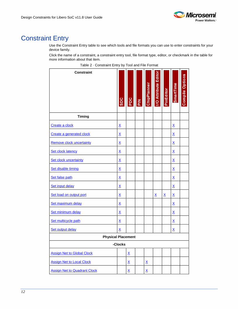
Constraint Entry Use the Constraint Entry table to see which tools and file formats you can use to enter constraints for your device family. Click the name of a constraint, a constraint entry tool, file format type, editor, or checkmark in the table for more information about that item.
Table 2 · Constraint Entry by Tool and File Format
Constraint
Timing
Create a clock X X
Create a generated clock X X
Remove clock uncertainty X X
Set clock latency X X
Set clock uncertainty X X
Set disable timing X X
Set false path X X
Set input delay X X
Set load on output port X X X X
Set maximum delay X X
Set minimum delay X X
Set multicycle path X X
Set output delay X X
Physical Placement
-Clocks
Assign Net to Global Clock X
Assign Net to Local Clock X X
Assign Net to Quadrant Clock X X
Design Constraints for Libero SoC v11.8 User Guide
13
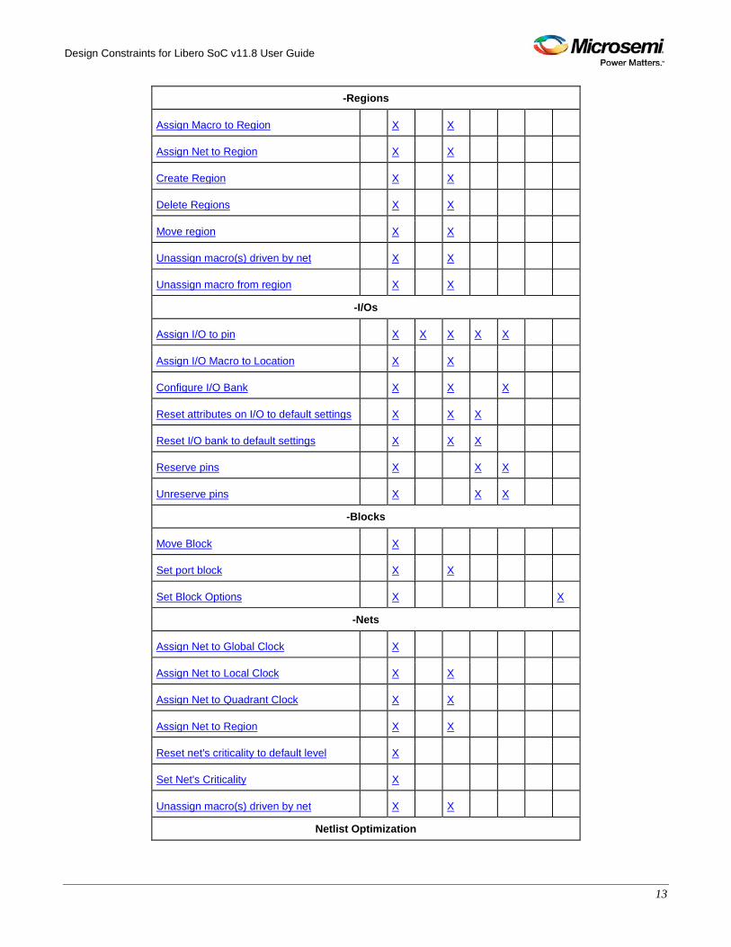
-Regions
Assign Macro to Region X X
Assign Net to Region X X
Create Region X X
Delete Regions X X
Move region X X
Unassign macro(s) driven by net X X
Unassign macro from region X X
-I/Os
Assign I/O to pin X X X X X
Assign I/O Macro to Location X X
Configure I/O Bank X X X
Reset attributes on I/O to default settings X X X
Reset I/O bank to default settings X X X
Reserve pins X X X
Unreserve pins X X X
-Blocks
Move Block X
Set port block X X
Set Block Options X X
-Nets
Assign Net to Global Clock X
Assign Net to Local Clock X X
Assign Net to Quadrant Clock X X
Assign Net to Region X X
Reset net's criticality to default level X
Set Net's Criticality X
Unassign macro(s) driven by net X X
Netlist Optimization
Design Constraints for Libero SoC v11.8 User Guide
14
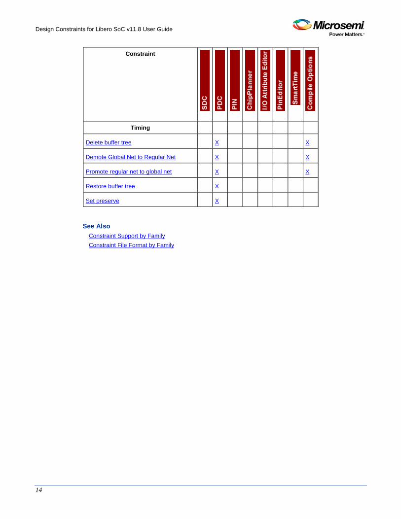
Constraint
Timing
Delete buffer tree X X
Demote Global Net to Regular Net X X
Promote regular net to global net X X
Restore buffer tree X
Set preserve X
See Also Constraint Support by Family Constraint File Format by Family
Design Constraints for Libero SoC v11.8 User Guide
15
Constraint File Format by Family Use the File Format by Family table to see which file formats apply to each type of constraint and each device family. When we specify a family name, we refer to the device family and all its derivatives, unless otherwise specified.
Table 3 · Constraint File Format by Family
Family Timing Physical Placement Netlist Optimiization
SDC PDC PDC
IGLOO X X
IGLOO2 X X X
SmartFusion2 X X X
SmartFusion and Fusion X X X
ProASIC3 X X
SDC – Synopsys Design Constraints PDC – Physical Design Constraints
See Also Constraint Support by Family Constraint Entry Table
Design Constraints for Libero SoC v11.8 User Guide
16
Basic Concepts
Naming Conventions The names of ports, instances, and nets in an imported netlist are sometimes referred to as their original names. Port names appear exactly as they are defined in a netlist. For example, a port named A/B appears as A/B in ChipPlanner, PinEditor, and I/O Attribute Editor in MultiView Navigator. Instances and nets display the original names plus an escape character (\) before each backslash (/) and each slash (\) that is not a hierarchy separator. For example, the instance named A/\B is displayed as A\/\\B. The following components use the Tcl-compliant original names: • PDC reader/writer • SDC reader/writer • Compile report • SDF/Netlist writer for back annotation • MultiView Navigator tools: NetlistViewer, PinEditor, ChipPlanner, and I/O Attribute Editor • SmartTime • SmartPower
See Also PDC Naming Conventions
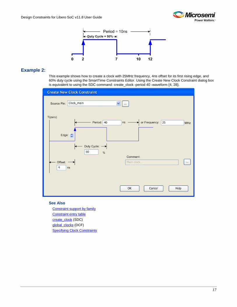
Clock Specifying clock constraints is the most effective way of constraining and verifying the timing behavior of a sequential design. You must use clock constraints to meet your performance goals and to quickly reach timing closure. Best practice is to specify and constrain all clocks used in the design. To create a clock constraint, you must provide the following clock information: Clock source: Specifies the pin or port where the clock signal is defined. Clock period or frequency: Defines the smallest amount of time after which the signal repeats itself. Duty cycle: Defines the percentage of time during which the clock period is high. First edge: Indicates whether the first edge of the clock is rising or falling. Offset: Indicates the shift of the first edge with respect to instant zero common to all clocks in the design.
Example 1: create_clock -period 10 -waveform {2 7} This example creates a clock with 10ns period, 2ns offset, and 50% duty cycle using the SDC command.
Design Constraints for Libero SoC v11.8 User Guide
17
Example 2: This example shows how to create a clock with 25MHz frequency, 4ns offset for its first rising edge, and 60% duty cycle using the SmartTime Constraints Editor. Using the Create New Clock Constraint dialog box is equivalent to using the SDC command: create_clock -period 40 -waveform {4, 28}.
See Also Constraint support by family Constraint entry table create_clock (SDC) global_clocks (DCF) Specifying Clock Constraints
Design Constraints for Libero SoC v11.8 User Guide
18
Region A region is a user-defined area on a chip into which you can constrain the physical placement of one or more macros. You can also constrain macros containing multiple tiles for cores, RAMs, and I/Os. The floorplanning process usually requires you to create several regions and assign logic to them. Logic can include core logic, memory, and I/O modules. When you run the place-and-route tool, it places the logic into their assigned regions. Some regions are user-defined and others are automatically created by the tools to meet routing requirements (for example, Local clock regions). You can use region constraints to:
• Create user-defined regions such as Inclusive, Exclusive, Empty, LocalClock, and QuadrantClock • Assign and unassign macros to user-defined regions • Constrain all the macros connected to a net by assigning them to a specific net region • Move regions from one set of co-ordinates to another
See Also Assign Macro to Region Create Region Delete Region Move Region Unassign macro from region About Floorplanning, Creating Regions, Editing Regions
Design Constraints for Libero SoC v11.8 User Guide
19
Location Each core, RAM, and I/O macro in the design is associated with a location on the device. When you run the place-and-route tool, it places all of your logic into their assigned locations. You can use location constraints to: • Overwrite the existing placements of macros • Tell the place-and-route tool where to initially place the macros • Assign I/O macros to specific pins to meet your board's requirements
See Also Assign I/O to pin Assign macro to location Assigning Logic to Locations, Moving Logic to Other Locations, Assigning Pins, Unassigning Pins
I/O Attributes I/O attributes are the characteristics of logic macros or nets in your design. They indicate placement, implementation, naming, directionality, and other characteristics. This information is used by the design implementation software during the place-and-route of a design. Input and output attributes are described in the documentation for the I/O Attribute Editor. Attributes applicable to a specific tool are described in the help for that tool. See the topics in I/O Attributes Reference for more detailed information about each attribute. See also , for a table of attributes for each device family, and Welcome to I/O Attribute Editor.
See Also I/O Attributes by Family I/O Standards and I/O Attributes Applicability I/O Standards Compatibility Matrix
Design Constraints for Libero SoC v11.8 User Guide
20
I/O Attributes
I/O Attributes by Family and Device Other than the four common attributes supported by all families, the following table includes the attributes that each Microsemi SoC family supports. The following table displays the attributes supported for each family. Note: Not all attributes apply to all banks for a given I/O standard. Refer to the appropriate datasheet for
details. Refer to the appropriate datasheet for information about I/O standards for different families.
Table 4 · I/O Attributes by Family and Device
Attribute Family
IGLOO SmartFusion2, IGLOO2, RTG4
SmartFusion and Fusion
ProASIC3
Bank Name X X X X
Direction X X X X
Group X X X X
Hold State X, IGLOO PLUS only
Hot Swappable X X X X
Input Delay X X X X, ProASIC3E and ProASIC3L only
I/O Available in Flash*Freeze Mode
X
I/O Standard X X X X
I/O State in Flash*Freeze Mode
X
Locked X X X X
Low Power Exit X
Macro Cell X X X
ODT Imp X
ODT Static X
Design Constraints for Libero SoC v11.8 User Guide
21
Attribute Family
IGLOO SmartFusion2, IGLOO2, RTG4
SmartFusion and Fusion
ProASIC3
Output Drive X X X X
Output Load X X X X
Pin Number X X X X
Port Name X X X X
Pre-Emphasis X
Resistor Pull X X X X
Schmitt Trigger X, IGLOOe and IGLOO PLUS only
X X X, ProASIC3e and ProASIC3L only
Skew X X X
Slew X X X X
Use Register X X X X
User Reserved X X X X, ProASIC3e and ProASIC3L only
Design Constraints for Libero SoC v11.8 User Guide
22
Bank Name
Purpose Displays the name of the bank to which the I/O macro has been assigned. You cannot change the bank name.
Families Supported
RTG4 X
IGLOO Yes
IGLOO2 Yes
SmarFusion2 Yes
SmartFusion Yes
Fusion Yes
ProASIC3 Yes
Direction
Purpose Indicates whether the pin is accepting a signal (input), sending a signal (output), or both sending and receiving a signal (Inout).
Families Supported
RTG4 Yes
IGLOO Yes
IGLOO2 Yes
SmartFusion2 Yes
SmartFusion Yes
Fusion Yes
ProASIC3 Yes
Design Constraints for Libero SoC v11.8 User Guide
23
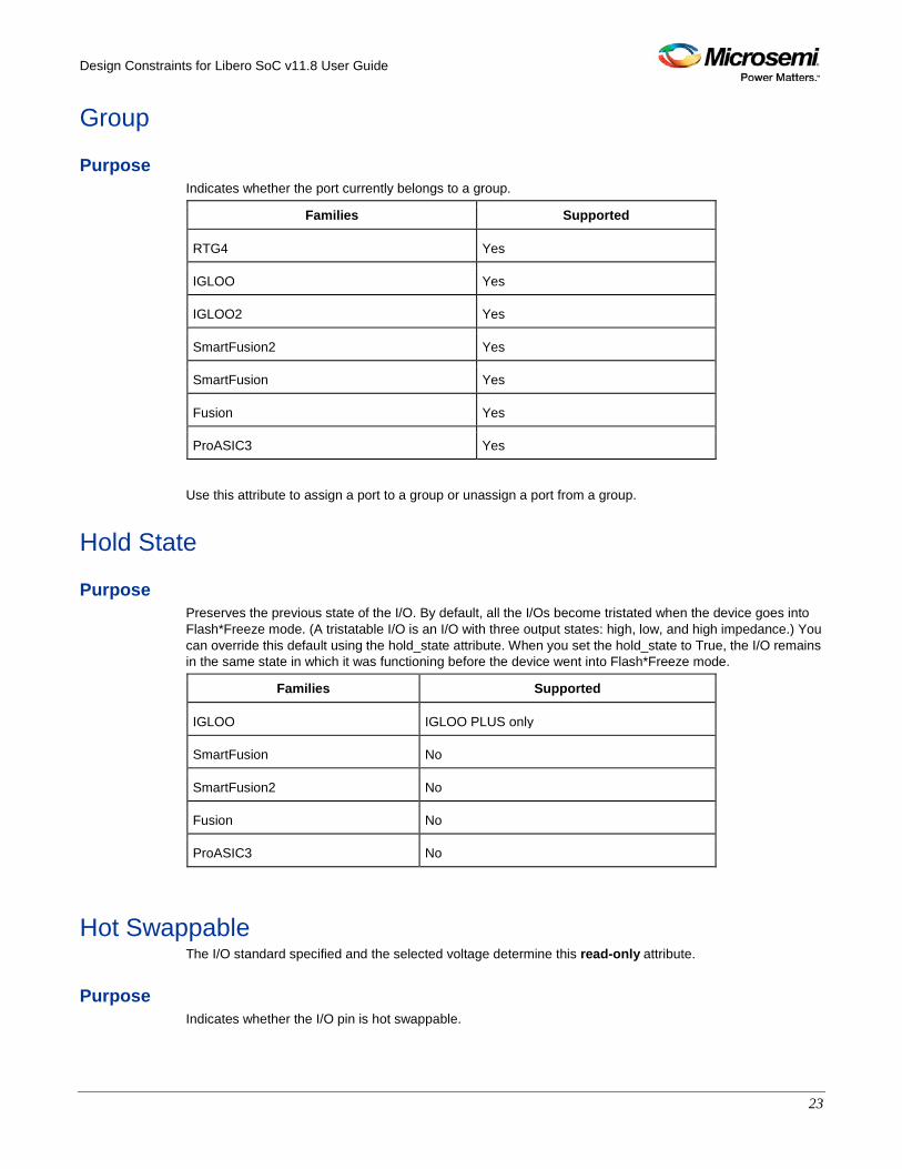
Group
Purpose Indicates whether the port currently belongs to a group.
Families Supported
RTG4 Yes
IGLOO Yes
IGLOO2 Yes
SmartFusion2 Yes
SmartFusion Yes
Fusion Yes
ProASIC3 Yes
Use this attribute to assign a port to a group or unassign a port from a group.
Hold State
Purpose Preserves the previous state of the I/O. By default, all the I/Os become tristated when the device goes into Flash*Freeze mode. (A tristatable I/O is an I/O with three output states: high, low, and high impedance.) You can override this default using the hold_state attribute. When you set the hold_state to True, the I/O remains in the same state in which it was functioning before the device went into Flash*Freeze mode.
Families Supported
IGLOO IGLOO PLUS only
SmartFusion No
SmartFusion2 No
Fusion No
ProASIC3 No
Hot Swappable The I/O standard specified and the selected voltage determine this read-only attribute.
Purpose Indicates whether the I/O pin is hot swappable.
Design Constraints for Libero SoC v11.8 User Guide
24
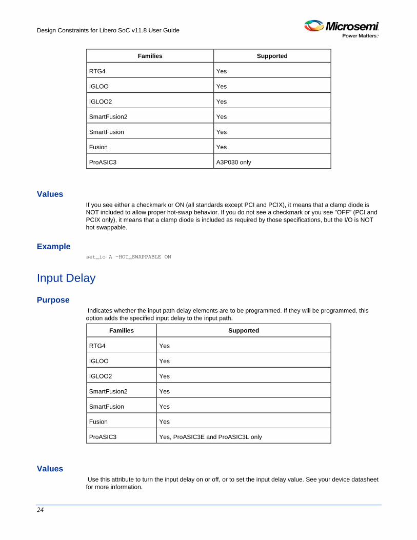
Families Supported
RTG4 Yes
IGLOO Yes
IGLOO2 Yes
SmartFusion2 Yes
SmartFusion Yes
Fusion Yes
ProASIC3 A3P030 only
Values If you see either a checkmark or ON (all standards except PCI and PCIX), it means that a clamp diode is NOT included to allow proper hot-swap behavior. If you do not see a checkmark or you see "OFF" (PCI and PCIX only), it means that a clamp diode is included as required by those specifications, but the I/O is NOT hot swappable.
Example set_io A -HOT_SWAPPABLE ON
Input Delay
Purpose Indicates whether the input path delay elements are to be programmed. If they will be programmed, this option adds the specified input delay to the input path.
Families Supported
RTG4 Yes
IGLOO Yes
IGLOO2 Yes
SmartFusion2 Yes
SmartFusion Yes
Fusion Yes
ProASIC3 Yes, ProASIC3E and ProASIC3L only
Values Use this attribute to turn the input delay on or off, or to set the input delay value. See your device datasheet for more information.
Design Constraints for Libero SoC v11.8 User Guide
25
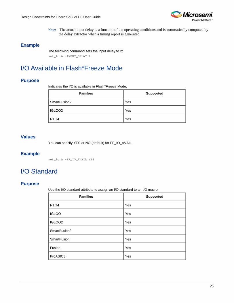
Note: The actual input delay is a function of the operating conditions and is automatically computed by the delay extractor when a timing report is generated.
Example The following command sets the input delay to 2: set_io A -INPUT_DELAY 2
I/O Available in Flash*Freeze Mode
Purpose Indicates the I/O is available in Flash*Freeze Mode.
Families Supported
SmartFusion2 Yes
IGLOO2 Yes
RTG4 Yes
Values You can specify YES or NO (default) for FF_IO_AVAIL.
Example set_io A -FF_IO_AVAIL YES
I/O Standard
Purpose Use the I/O standard attribute to assign an I/O standard to an I/O macro.
Families Supported
RTG4 Yes
IGLOO Yes
IGLOO2 Yes
SmartFusion2 Yes
SmartFusion Yes
Fusion Yes
ProASIC3 Yes
Design Constraints for Libero SoC v11.8 User Guide
26
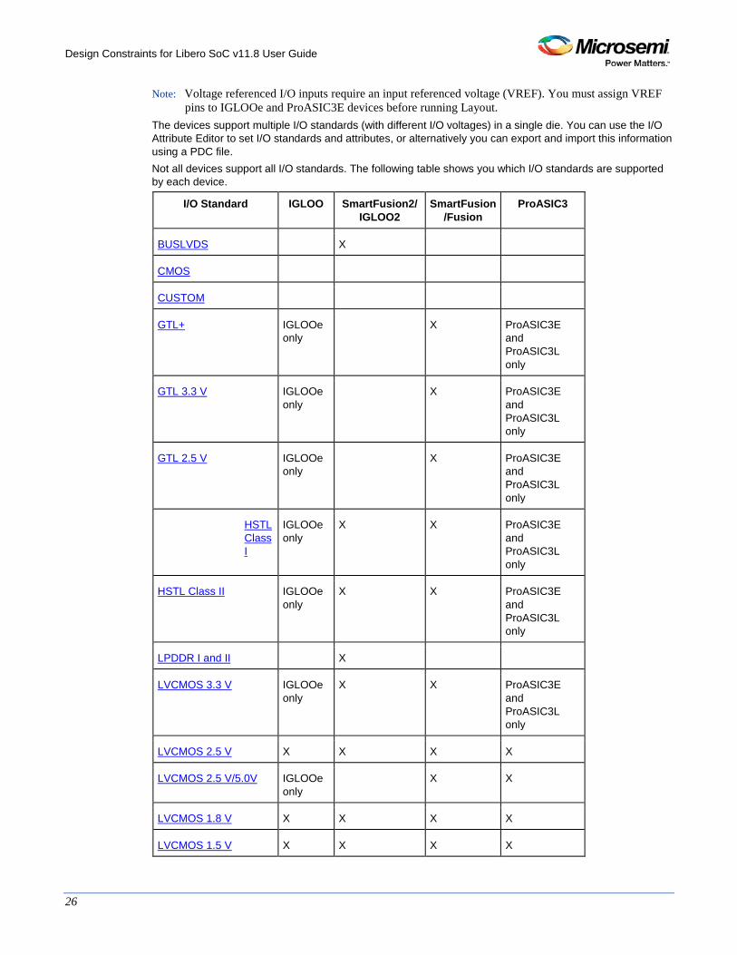
Note: Voltage referenced I/O inputs require an input referenced voltage (VREF). You must assign VREF pins to IGLOOe and ProASIC3E devices before running Layout.
The devices support multiple I/O standards (with different I/O voltages) in a single die. You can use the I/O Attribute Editor to set I/O standards and attributes, or alternatively you can export and import this information using a PDC file. Not all devices support all I/O standards. The following table shows you which I/O standards are supported by each device.
I/O Standard IGLOO SmartFusion2/ IGLOO2
SmartFusion /Fusion
ProASIC3
BUSLVDS X
CMOS
CUSTOM
GTL+ IGLOOe only
X ProASIC3E and ProASIC3L only
GTL 3.3 V IGLOOe only
X ProASIC3E and ProASIC3L only
GTL 2.5 V IGLOOe only
X ProASIC3E and ProASIC3L only
HSTL Class I
IGLOOe only
X X ProASIC3E and ProASIC3L only
HSTL Class II IGLOOe only
X X ProASIC3E and ProASIC3L only
LPDDR I and II X
LVCMOS 3.3 V IGLOOe only
X X ProASIC3E and ProASIC3L only
LVCMOS 2.5 V X X X X
LVCMOS 2.5 V/5.0V IGLOOe only
X X
LVCMOS 1.8 V X X X X
LVCMOS 1.5 V X X X X
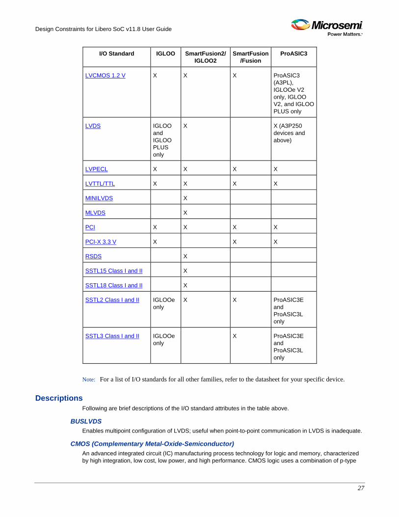
Design Constraints for Libero SoC v11.8 User Guide
27
I/O Standard IGLOO SmartFusion2/ IGLOO2
SmartFusion /Fusion
ProASIC3
LVCMOS 1.2 V X X X ProASIC3 (A3PL), IGLOOe V2 only, IGLOO V2, and IGLOO PLUS only
LVDS IGLOO and IGLOO PLUS only
X X (A3P250 devices and above)
LVPECL X X X X
LVTTL/TTL X X X X
MINILVDS X
MLVDS X
PCI X X X X
PCI-X 3.3 V X X X
RSDS X
SSTL15 Class I and II X
SSTL18 Class I and II X
SSTL2 Class I and II IGLOOe only
X X ProASIC3E and ProASIC3L only
SSTL3 Class I and II IGLOOe only
X ProASIC3E and ProASIC3L only
Note: For a list of I/O standards for all other families, refer to the datasheet for your specific device.
Descriptions Following are brief descriptions of the I/O standard attributes in the table above.
BUSLVDS Enables multipoint configuration of LVDS; useful when point-to-point communication in LVDS is inadequate.
CMOS (Complementary Metal-Oxide-Semiconductor) An advanced integrated circuit (IC) manufacturing process technology for logic and memory, characterized by high integration, low cost, low power, and high performance. CMOS logic uses a combination of p-type
Design Constraints for Libero SoC v11.8 User Guide
28
and n-type metal-oxide-semiconductor field effect transistors (MOSFETs) to implement logic gates and other digital circuits found in computers, telecommunications, and signal processing equipment.
CUSTOM An option in the I/O Attribute Editor that enables you to customize individual I/O settings such as the I/O threshold, output slew rates, and capacitive loadings on an individual I/O basis. For example, PCI mode output can be set to low-slew rate. For more information, go to the Microsemi SoC web site and check the datasheet for your device.
GTL 2.5 V (Gunning Transceiver Logic 2.5 Volts) A low-power standard (JESD 8.3) for electrical signals used in CMOS circuits that allows for low electromagnetic interference at high speeds of transfer. It has a voltage swing between 0.4 volts and 1.2 volts, and typically operates at speeds of between 20 and 40MHz. The VCCI must be connected to 2.5 volts.
GTL 3.3 V (Gunning Transceiver Logic 3.3 Volts) Same as GTL 2.5 V above, except the VCCI must be connected to 3.3 volts.
GTL+ (Gunning Transceiver Logic Plus) An enhanced version of GTL that has defined slew rates and higher voltage levels. It requires a differential amplifier input buffer and an open-drain output buffer. Even though output is open-drain, the VCCI must be connected to either 2.5 volts or 3.3 volts for SmartFusion, IGLOO, ProASIC3 and Fusion families.
HSTL Class I and II (High-Speed Transceiver Logic) A general-purpose, high-speed 1.5 V bus standard (EIA/JESD 8-6) for signalling between integrated circuits. The signalling range is 0 V to 1.5 V, and signals can be either single-ended or differential. HSTL requires a differential amplifier input buffer and a push-pull output buffer. It has four classes, of which Microsemi SoC supports Class I and II. These classes are defined by standard EIA/JESD 8-6 from the Electronic Industries Alliance (EIA):
• Class I (unterminated or symmetrically parallel terminated) • Class II (series terminated) • Class III (asymmetrically parallel terminated) • Class IV (asymmetrically double parallel terminated
LPDDR I and II Low Power double data rate synchronous DRAM for mobile computers.
LVCMOS 3.3 V (Low-Voltage CMOS for 3.3 Volts) An extension of the LVCMOS standard (JESD 8-5) used for general-purpose 3.3 V applications.
LVCMOS 2.5 V (Low-Voltage CMOS for 2.5 Volts) An extension of the LVCMOS standard (JESD 8-5) used for general-purpose 2.5 V applications.
LVCMOS 2.5 V/5.5V (Low-Voltage CMOS for 2.5 and 5.0 Volts) An extension of the LVCMOS standard (JESD 8-5) used for general-purpose 2.5 V and 5.0V applications.
LVCMOS 1.8 V (Low-Voltage CMOS for 1.8 Volts) An extension of the LVCMOS standard (JESD 8-5) used for general-purpose 1.8 V applications. It uses a 3.3 V-tolerant CMOS input buffer and a push-pull output buffer.
LVCMOS 1.5 V (Low-Voltage CMOS for 1.5 volts) An extension of the LVCMOS standard (JESD 8-5) used for general-purpose 1.5 V applications. It uses a 3.3 V-tolerant CMOS input buffer and a push-pull output buffer.
LVCMOS 1.2 V (Low-Voltage CMOS for 1.2 volts) Note: An extension of the LVCMOS standard (JESD 8-5) used for general-purpose 1.2 V applications.
Design Constraints for Libero SoC v11.8 User Guide
29
Note: 1.2 voltage is supported for ProASIC3 (A3PL), IGLOOe V2 only, IGLOO V2, and IGLOO PLUS.
LVDS (Low-Voltage Differential Signal) A moderate-speed differential signalling system, in which the transmitter generates two different voltages which are compared at the receiver. It requires that one data bit be carried through two signal lines; therefore, you need two pins per input or output. It also requires an external resistor termination. The voltage swing between these two signal lines is approximately 350mV (millivolts).
LVPECL (Low-Voltage Positive Emitter Coupled Logic) PECL is another differential I/O standard. It requires that one data bit is carried through two signal lines; therefore, two pins are needed per input or output. It also requires an external resistor termination. The voltage swing between these two signal lines is approximately 850mV. When the power supply is +3.3 V, it is commonly referred to as low-voltage PECL (LVPECL).
LVTTL/TTL (Low-Voltage Transitor-Transistor Level) A general purpose standard (EIA/JESDSA) for 3.3 V applications. It uses an LVTTL input buffer and a push-pull output buffer.
MINILVDS Signaling standard used for display applications with resolutions between video graphics arrays (VGAs) and ultra extended graphic arrays (UXGAs).
MLVDS MLVDS has two types of receivers. Type-1 is compatible with LVDS and uses a +/- 50 mV threshold. Type-2 receivers allow Wired-Or signaling with M-LVDS devices. For MLVDS:
PCI (Peripheral Component Interface) A computer bus for attaching peripheral devices to a computer motherboard in a local bus. This standard supports both 33 MHz and 66 MHz PCI bus applications. It uses an LVTTL input buffer and a push-pull output buffer. With the aid of an external resistor, this I/O standard can be 5V-compliant for most families, excluding ProASIC3 families.
PCI-X (Peripheral Component Interface Extended) An enhanced version of the PCI specification that can support higher average bandwidth; it increases the speed that data can move within a computer from 66 MHz to 133 MHz. PCI-X is backward-compatible, which means that devices can operate at conventional PCI frequencies (33 MHz and 66 MHz). PCI-X is also more fault-tolerant than PCI.
RSDS Reduced Swing Differential Signaling , a electronic signaling standard and protocol for a chip-to-chip interface. Signaling standard commonly used for display applications with resolutions between video graphics arrays (VGAs) and ultra extended graphic arrays (UXGAs).
SSTL15 Class I and II I/O standard with a voltage-referenced signal, input (VREF) of 0.75, and an output (VCCIO) voltage of 1.5 V.
SSTL18 Class I and II SSTL is an electrical interface commonly used with DDR [Double Data Rate] DRAM memory ICs and memory modules. SSTL_18 Series Stub Terminated, used with DDR II memory; requires Vddq = 1.8v, Vt = 0.5 x Vddq
SSTL2 Class I and II (Stub Series Terminated Logic 2.5 V) A general-purpose 2.5 V memory bus standard (JESD 8-9) for driving transmission lines. This standard was designed specifically for driving the DDR (double-data-rate) SDRAM modules used in computer memory. It requires a differential amplifier input buffer and a push-pull output buffer. It has two classes; Microsemi SoC supports both.
Design Constraints for Libero SoC v11.8 User Guide
30
SSTL3 Class I and II (Stub Series Terminated Logic for 3.3 V) A general-purpose 3.3 V memory bus standard (JESD 8-8) for driving transmission lines.
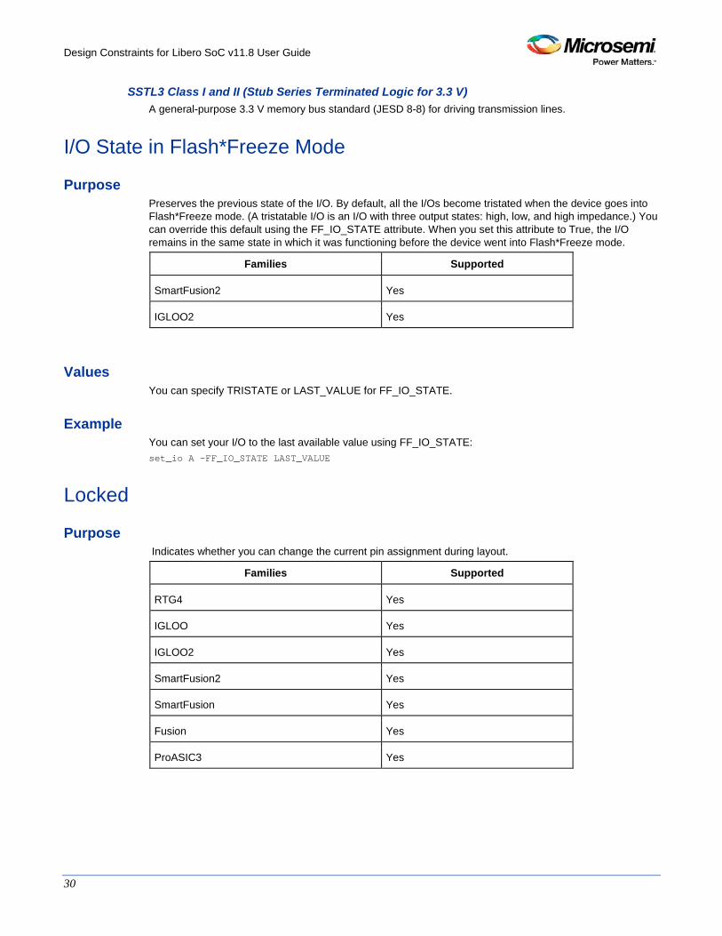
I/O State in Flash*Freeze Mode
Purpose Preserves the previous state of the I/O. By default, all the I/Os become tristated when the device goes into Flash*Freeze mode. (A tristatable I/O is an I/O with three output states: high, low, and high impedance.) You can override this default using the FF_IO_STATE attribute. When you set this attribute to True, the I/O remains in the same state in which it was functioning before the device went into Flash*Freeze mode.
Families Supported
SmartFusion2 Yes
IGLOO2 Yes
Values You can specify TRISTATE or LAST_VALUE for FF_IO_STATE.
Example You can set your I/O to the last available value using FF_IO_STATE: set_io A -FF_IO_STATE LAST_VALUE
Locked
Purpose Indicates whether you can change the current pin assignment during layout.
Families Supported
RTG4 Yes
IGLOO Yes
IGLOO2 Yes
SmartFusion2 Yes
SmartFusion Yes
Fusion Yes
ProASIC3 Yes
Design Constraints for Libero SoC v11.8 User Guide
31
Values Use this attribute to lock or unlock the pin assignment. Selecting the check box locks the pin assignment. Clearing the check box unlocks the pin assignment. If locked, you cannot change the pin assignment. PDC values are YES or NO.
Example set_io -fixed YES
Low Power Exit
Purpose Sets the state at which your device exits from Low Power mode.
Families Supported
RTG4 Yes
SmartFusion2 Yes
IGLOO2 Yes
Values You can set Low Power Exit to OFF (default), Wake_on_Change, Wake_on_0, or Wake_on_1. For example: set_io A -LPE Wake_on_1
Macro Cell
Purpose Indicates the type of I/O macro. This value is read only and is applicable only to the I/O Attribute Editor tool (that is, you cannot use it in PDC files).
Families Supported
IGLOO Yes
SmartFusion Yes
Fusion Yes
ProASIC3 Yes
Design Constraints for Libero SoC v11.8 User Guide
32
ODT Imp
Purpose On-die termination (ODT) is the technology where the termination resistor for impedance matching in transmission lines is located inside a semiconductor chip instead of on a printed circuit board. Port Configuration (PC) bits are static configuration bits set during programming to configure the IO(s) as per your choice.
Families Supported
RTG4 Yes
SmartFusion2 Yes
IGLOO2 Yes
Values See the device datasheet for available values.
Example You can set your ODT Imp to 50 with the following command: set_io Y -ODT_IMP 50
ODT Static
Purpose On-die termination (ODT) is the technology where the termination resistor for impedance matching in transmission lines is located inside a semiconductor chip instead of on a printed circuit board.
Families Supported
RTG4 Yes
SmartFusion2 Yes
IGLOO2 Yes
Values On or Off (default).
Example Set your ODT Static to On with the following command: set_io A -ODT_STATIC On
Design Constraints for Libero SoC v11.8 User Guide
33
Output Drive
Purpose Every I/O standard has an output drive preset; however, for some I/O standards, you can choose which one to use. The higher the drive, the faster the I/O. The faster the I/O, the more power consumed by the I/O.
Families Supported
RTG4 Yes
IGLOO Yes
IGLOO2 Yes
SmartFusion2 Yes
SmartFusion Yes
Fusion Yes
ProASIC3 Yes
Values Drive strength is programmable for some I/O technologies. See the device silicon user's guide for specific ranges. Some I/O technologies are not programmable. Using this attribute in conjunction with non-programmable I/O technology will generate an error no matter what value the attribute is set to.
Example set_io -out_drive 4
Output Load
Purpose Indicates the output-capacitance value based on the I/O standard selected in the I/O Standard cell. This option is not available in software.
Families Supported
RTG4 Yes
IGLOO Yes
IGLOO2 Yes
SmartFusion2 Yes
SmartFusion Yes
Fusion Yes
Design Constraints for Libero SoC v11.8 User Guide
34
Families Supported
ProASIC3 Yes
Values You can enter a capacitative load as an integral number of picofarads. The default value varies by device family. If necessary, you can change the output capacitance default setting to improve timing definition and analysis. Both the capacitive loading on the board and the Vil/Vih trip points of driven devices affect output-propagation delay. SmartTime, Timing-Driven Layout and Back-Annotation automatically uses the modified delay model for delay calculations. The default value is 5, and the range of possible values is 0-9999.
Example -set_io Y -OUT_LOAD 5
Pin Number
Purpose Use this attribute to change a pin assignment by choosing one of the legal values from the drop-down list. If the pin has been assigned, the pin number appears in this column. If it has not been assigned then Unassigned appears in this column.
Families Supported
RTG4 Yes
IGLOO Yes
IGLOO2 Yes
SmartFusion2 Yes
SmartFusion Yes
Fusion Yes
ProASIC3 Yes
Example set_io -pinname AC30
Design Constraints for Libero SoC v11.8 User Guide
35
Port Name
Purpose Indicates the port name of the I/O macro. This value is read only.
Families Supported
RTG4 Yes
IGLOO Yes
IGLOO2 Yes
SmartFusion2 Yes
SmartFusion Yes
Fusion Yes
ProASIC3 Yes
Pre-Emphasis The pre-emphasis rate is the amount of rise or fall time an input signal takes to get from logic low to logic high or vice versa. It is commonly defined to be the propagation delay between 10% and 90% of the signal's voltage swing.
Purpose Indicates the slew rate for output buffers. Generally, available slew rates are high and low.
Families Supported
RTG4 Yes
SmartFusion2 Yes
IGLOO2 Yes
Values You can set the slew rate for the output buffer to NONE (default), MIN, MEDIUM, or MAX. The output buffer has a programmable slew rate for both high-to-low and low-to-high transitions. The low rate is incompatible with 3.3 V PCI requirements. Not all I/O technologies support pre-emphasis; including the attribute in a set_io statement that specified a non-supporting I/O technology will create an error. For SmartFusion2 you can edit the pre-emphasis for designs using LVTTL, all LVCMOS, or PCIX I/O standards. One way to eliminate problems with low slew rate is with external . In processing electronic audio signals, pre-emphasis refers to a system process designed to increase (within a frequency band) the magnitude of some (usually higher) frequencies with respect to the magnitude of other (usually lower) frequencies in order to improve the overall signal-to-noise ratio by minimizing the adverse effects of such phenomena as attenuation distortion or saturation of recording media in subsequent
Design Constraints for Libero SoC v11.8 User Guide
36
parts of the system. While the mirror operation is called de-emphasis, the system as a whole is called emphasis.
Example set_io A -PRE_EMPHASIS NONE
Resistor Pull
Purpose Allows inclusion of a weak resistor for either pull-up or pull-down of the input buffer.
Families Supported
RTG4 Yes
IGLOO Yes
IGLOO2 Yes
SmartFusion2 Yes
SmartFusion Yes
Fusion Yes
ProASIC3 Yes
Values Use this attribute to set the resistor pull. Your choices are None, Up (pull-up), or Down (pull-down). The default value is None, except when an I/O exists in the netlist as a port, is not connected to the core, and is configured as an output buffer. In that case, the default setting is for a weak pull-down.
Example -set_io A -RES_PULL NONE
Schmitt Trigger
Purpose A schmitt trigger is a buffer used to convert a slow or noisy input signal into a clean one before passing it to the FPGA. This is a simple, low-cost solution for a user working with low slew-rate signals. Using schmitt-trigger buffers guarantees a fast, noise-free, input signal to the FPGA. Schmitt-trigger buffers are categorized in three configurations:
• Fixed threshold voltages with non-inverted outputs • Fixed threshold voltages and inverted outputs • Variable threshold voltages with non-inverted outputs
With the aid of schmitt-trigger buffers, low slew-rate applications can also be handled with ease. Implementation of these buffers is simple, not expensive, and flexible in that different configurations are
Design Constraints for Libero SoC v11.8 User Guide
37
possible depending on the application. The characteristics of schmitt-trigger buffers (e.g. threshold voltage) can be fixed or user-adjustable if required.
Families Supported
RTG4 Yes
IGLOO Yes, IGLOOe and IGLOO PLUS only
IGLOO2 Yes
SmartFusion2 Yes
SmartFusion Yes
Fusion Yes
ProASIC3 Yes, with one exception: this attribute is not supported in ProASIC3L except in A3PE3000L
Values A schmitt trigger has two possible states: Off (default) or On. The trigger for this circuit to change states is the input voltage level. That is, the output state depends on the input level, and will change only as the input crosses a pre-defined threshold. Not all I/O technologies support SCHMITT_TRIGGER. Including the attribute in a set_io statement that also specifies a non-supporting I/O technology will create an error. For more information, please see the Using Schmitt Triggers for Low Slew-Rate Input Application Note on the Microsemi SoC web site.
Example set_io A -SCHMITT_TRIGGER On
Skew
Purpose Indicates whether there is a fixed additional delay between the enable/disable time for a tristatable I/O. (A tristatable I/O is an I/O with three output states: high, low, and high impedance.) 2 ns delay on rising edge, 0 ns delay on falling edge.
Families Supported
IGLOO Yes
SmartFusion Yes
Fusion Yes
ProASIC3 Yes
Design Constraints for Libero SoC v11.8 User Guide
38
Values You can set the skew for a clock to either Off (default) or On. Note that a Tri State or "tristatable" logic gate has three output states: high, low, and high impedance. In a high impedance state, the output acts like a resistor with infinite resistance, which means the output is disconnected from the rest of the circuit.
Example -set_io -skew On
Slew The slew rate is the amount of rise or fall time an input signal takes to get from logic low to logic high or vice versa. It is commonly defined to be the propagation delay between 10% and 90% of the signal's voltage swing.
Purpose Indicates the slew rate for output buffers. Generally, available slew rates are high and low.
Families Supported
RTG4 Yes
SmartFusion2 Yes
IGLOO2 Yes
IGLOO Yes
SmartFusion Yes
Fusion Yes
ProASIC3 Yes
Values Values for slew for SF2 are: SLOW (default), MEDIUM, MEDIUM_FAST, and FAST. MSIO and MSIOD banks only accept SLOW for SLEW values on the I/O technologies that support SLEW. DDRIO supports all four values. Not all I/O technologies support SLEW. Including the attribute in a set_io statement that also specifies a non-supporting I/O technology will create an error. The SLOW slew rate is incompatible with 3.3 V PCI requirements. For ProASIC3 families, you can edit the slew for designs using LVTTL, all LVCMOS, or PCIX I/O standards. The other I/O standards have a preset slew value. For those devices that support additional slew values, Microsemi SoC recommends that you use the SLOW and FAST values and let the software map to the appropriate absolute slew value. The default slew displayed in the I/O Attribute Editor is based on the selected I/O standard. For example, PCI mode sets the default output slew rate to FAST. Note: One way to eliminate problems with low slew rate is with external . In some applications, you may require a very fast (i.e. high slew rate) signal, which approaches an ideal switching transition. You can accomplish this by either reducing the track resistance and/or capacitance on the board or increasing the drive capability of the input signal. Both of these options are generally time
Design Constraints for Libero SoC v11.8 User Guide
39
consuming and costly. Furthermore, the closer the input signal approaches an ideal one, the greater the likelihood of unwanted effects such as increased peak current, capacitive coupling, and ground bounce. In many cases, you may want to incorporate a finite amount of slew rate into your signal to reduce these effects. On the other hand, if an input signal becomes too slow (i.e. low slew rate), then noise around the FPGA's input voltage threshold can cause multiple state changes. During the transition time, both input buffer transistors could potentially turn on at the same time, which could result in the output of the buffer to oscillate unpredictably. In this situation, the input buffer could still pass signals. However, these short, unpredictable oscillations would likely cause the device to malfunction.
Example -set_io slew MEDIUM
Use Register
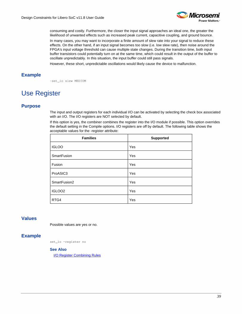
Purpose The input and output registers for each individual I/O can be activated by selecting the check box associated with an I/O. The I/O registers are NOT selected by default. If this option is yes, the combiner combines the register into the I/O module if possible. This option overrides the default setting in the Compile options. I/O registers are off by default. The following table shows the acceptable values for the -register attribute:
Families Supported
IGLOO Yes
SmartFusion Yes
Fusion Yes
ProASIC3 Yes
SmartFusion2 Yes
IGLOO2 Yes
RTG4 Yes
Values Possible values are yes or no.
Example set_io -register no
See Also I/O Register Combining Rules
Design Constraints for Libero SoC v11.8 User Guide
40
User Reserved
Purpose You can explicitly reserve a pin in one of the following ways: • In the I/O Attribute Editor (Package Pins view), select the User Reserved checkbox associated with
the pin to reserve. • Select a pin in PinEditor, right-click it, and choose Reserve Pin from the right-click menu. • Use the reserve command in a PDC file.
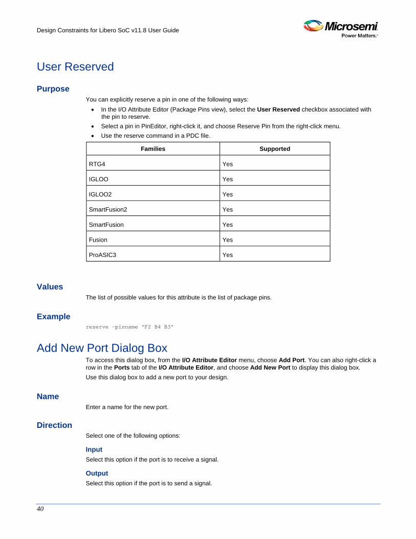
Families Supported
RTG4 Yes
IGLOO Yes
IGLOO2 Yes
SmartFusion2 Yes
SmartFusion Yes
Fusion Yes
ProASIC3 Yes
Values The list of possible values for this attribute is the list of package pins.
Example reserve -pinname "F2 B4 B3"
Add New Port Dialog Box To access this dialog box, from the I/O Attribute Editor menu, choose Add Port. You can also right-click a row in the Ports tab of the I/O Attribute Editor, and choose Add New Port to display this dialog box. Use this dialog box to add a new port to your design.
Name Enter a name for the new port.
Direction Select one of the following options:
Input Select this option if the port is to receive a signal.
Output Select this option if the port is to send a signal.
Design Constraints for Libero SoC v11.8 User Guide
41
Bi-directional (Inout) Select this option if the port will both send and receive a signal.
Modify Port Dialog Box To access this dialog box, from the I/O Attribute Editor menu, choose Modify Port. You can also right-click a row in the Ports tab of the I/O Attribute Editor, and choose Modify Port to display this dialog box. Use this dialog box to modify the name or direction of an existing port in your design.
Name Enter a new name for the port.
Direction Select one of the following options:
Input Select this option if the port is to receive a signal.
Output Select this option if the port is to send a signal.
Bi-directional (Inout) Select this option if the port will both send and receive a signal.
Design Constraints for Libero SoC v11.8 User Guide
42
I/O Bank Settings Dialog Box (IGLOO and ProASIC3 only) To access this dialog, from the Edit menu, choose I/O Bank Settings. Use this dialog box to assign I/O technologies to I/O banks in IGLOO (excluding IGLOOe) and ProASIC3 (excluding ProASIC3L and ProASIC3E) devices.
Choose Bank Choose a bank from the drop-down list.Any banks not assigned I/O standards use the default standard selected in your Project Settings.
Locked Select this option to lock all I/O banks, so the I/O Bank Assigner cannot unassign and re-assign the technologies in your design.
Select All Technologies That the Bank Should Support Selecting an I/O standard selects all compatible standards and grays out incompatible ones. For example, selecting LVTTL also selects PCI, PCIX, and LVPECL, since they all have the same VCCI. Further, selecting GTLP (3.3V) disables SSTL3 as an option because the VREFs of the two are not the same.
VCCI Each I/O bank has a common supply voltage, VCCI, for the I/Os within that bank. Click Apply to assign the selected I/O standards to the selected bank. Any previously assigned I/Os in the bank that are no longer compatible with the standards applied are unassigned.
See Also Manually Assigning Technologies to I/O Banks Assigning VREF Pins
Design Constraints for Libero SoC v11.8 User Guide
43
I/O Bank Settings Dialog Box To access this dialog, from the Edit menu, choose I/O Bank Settings. Use this dialog box to assign I/O technologies to I/O banks in IGLOOe, Fusion, ProASIC3L, and ProASIC3E devices.
Choose Bank Choose a bank from the drop-down list. If you do not assign I/O standards to a bank, that bank uses the default standard selected in the Device Selection Wizard.
Locked Select this option to lock all I/O banks, so the I/O Bank Assigner cannot unassign and re-assign the technologies in your design.
Select All Technologies That the Bank Should Support Selecting an I/O standard selects all compatible standards and grays out incompatible ones. For example, selecting LVTTL also selects PCI, PCIX, and LVPECL, since they all have the same VCCI. Further, selecting GTLP (3.3V) disables SSTL3 as an option because the VREFs of the two are not the same.
VCCI Each I/O bank has a common supply voltage, VCCI, for the I/Os within that bank. (Technologies not allowed for the selected VCCI appear grayed out.)
VREF A voltage referenced I/O input (VREF) requires an input referenced voltage. You must assign VREF pins to IGLOOe, Fusion, ProASIC3L (A3PE3000L only) and ProASIC3E devices before running Layout. Note: You cannot assign VREF pins in IGLOO or ProASIC3 low-cost devices.
Use Default Pins for VREFs Select this check box to set default VREF pins and unset non-default VREF pins. If you unselect this option when setting a new VREF technology, no VREF pins are set. If you unselect this option when default VREF pins are already set, it unsets them. Click More Attributes to set the low-power mode and input delay. (These attributes are not supported in IGLOOe, Fusion, or ProASIC3E devices.) Click Apply to assign the selected I/O standards to the selected bank. Any previously assigned I/Os in the bank that are no longer compatible with the standards applied are unassigned.
See Also Manually Assigning Technologies to I/O Banks Assigning Pins in IGLOOe, Fusion, and ProASIC3E Assigning VREF Pins
I/O Bank Settings for the SmartDesign Microcontroller Subsystem (MSS)
To access the I/O Bank settings in your MSS design you must click the I/O Editor tab in the MSS configurator. You can use the I/O Bank Settings dialog box to change the VCCI of the banks where the MSS I/Os are placed. You have four options:
• 1.50V • 1.80V
Design Constraints for Libero SoC v11.8 User Guide
44
• 2.50V • 3.30V
East MSS I/Os refer to Bank2. West MSS I/Os refer to Bank4. When changing the VCCI the MSS I/Os placed on this bank will change the IoTech to match the new VCCI; this is done automatically. The IoTech is changed as follows: • 3.30V: MSS I/Os placed on this bank are changed to LVTTL. • 2.50V: MSS I/Os placed on this bank are changed to LVCMOS 2.5V. • 1.80V: MSS I/Os placed on this bank are changed to LVCMOS 1.8V. • 1.50V: MSS I/Os placed on this bank are changed to LVCMOS 1.5V.
Design Constraints for Libero SoC v11.8 User Guide
45
Entering Constraints
You can enter design constraints in the following ways: • Importing constraint files: You can import - PDC or SDC constraint files for SmartFusion2, IGLOO2,
RTG4, SmartFusion, IGLOO, ProASIC3, Fusion families. • Using constraint editor tools: The constraint editor is a graphical user interface (GUI) tools for
creating and modifying physical, logical, and timing constraints. Using these tools enables you to enter constraints without having to understand PDC or other file syntax. The constraints you enter in the interactive tools are saved in a PDC or SDC file inside the Libero SoC project.
For SmartFusion, IGLOO, ProASIC3, Fusion, use the tools within the MultiView Navigator: - ChipPlanner - Sets location and region assignments - PinEditor in MVN - Sets the pin location constraints - I/O Attribute Editor - Sets I/O attributes - SmartTime Constraints Editor - Enables you to view and edit timing constraints
For SmartFusion2, IGLOO2, RTG4 constraints in Classic Constraint Flow, see the SmartFusion2-specific content. For SmartFusion2, IGLOO2, RTG4 constraints in Enhanced Constraint Flow, see Constraint Manager.
See Also Constraint Support by Family Constraint Entry Constraint File Format by Family Designer Naming Conventions
Design Constraints for Libero SoC v11.8 User Guide
46
Importing Constraint Files For details about how to import Constraint Files into a Libero SoC Enhanced Constraint Flow project, see Constraint Manager. For all other Libero SoC projects, you can import a constraint file as either a source file or an auxiliary file.
Source File Import constraints file as source files if they were created with external tools that will be tracked (audited). This helps to coordinate the design changes better. The following table shows different constraints format files that can be imported as source files for specific families.
Table 5 · File Types You Can Imported as Source Files
Source Files File Type Extension
Family
Physical Design Constraint File
*.pdc SmartFusion2, IGLOO2, RTG4, SmartFusion, IGLOO, ProASIC3, Fusion
Synopsys Constraint File
*.sdc SmartFusion2, IGLOO2, RTG4, SmartFusion, IGLOO, ProASIC3, Fusion
Auxiliary File When you import a constraint file as an auxiliary file, it is not audited and is treated more as one-time data-entry or data-change events, similar to entering data using one of the interactive editors. The following table shows different constraints format files that can be imported as auxiliary files for specific families.
Table 6 · File Types You Can Import as Auxiliary Files
Auxiliary Files File Type Extension
Family
SDC *.sdc SmartFusion, IGLOO, ProASIC3, Fusion
Physical Design Constraint** *.pdc IGLOO, Fusion, ProASIC3
Switching Activity Intermediate File/Format
*.saif IGLOO, Fusion, ProASIC3
Value Change Dump file *.vcd IGLOO, Fusion, ProASIC3
(*) When you import SDC as an auxiliary file, you can specify only one file in the File > Import Auxiliary Files dialog box. (**) Not all PDC commands are supported when a PDC file is imported as an auxiliary file; some must be imported as source files. When importing a PDC file as an auxiliary file, the new or modified PDC constraints are merged with the existing constraints. The software resolves any conflicts between new and existing physical constraints and displays the appropriate message. Most PDC commands can be imported as auxiliary files. PDC commands that are not supported when the PDC file is imported as an auxiliary file are noted in their respective help topics. You can either overwrite or retain your existing timing and physical constraints.
Design Constraints for Libero SoC v11.8 User Guide
47
See Also Importing source files Importing auxiliary files Keep Existing Timing Constraints Keep Existing Physical Constraints
About SmartTime Constraints Editor SmartTime Constraints Editor is an interface that enables you to view and edit timing constraints. Use this editor to view, edit, and create timing constraints used by the SmartTime timing analysis and timing-driven optimization tools. The editor includes powerful visual dialogs that guide you toward capturing your timing requirements and timing exceptions quickly and correctly. The editor is also closely connected to the analysis view of SmartTime (SmartTime Timing Analyzer) that enables you to quickly analyze the impact of constraint changes.
Design Constraints for Libero SoC v11.8 User Guide
48
Exporting Constraint Files
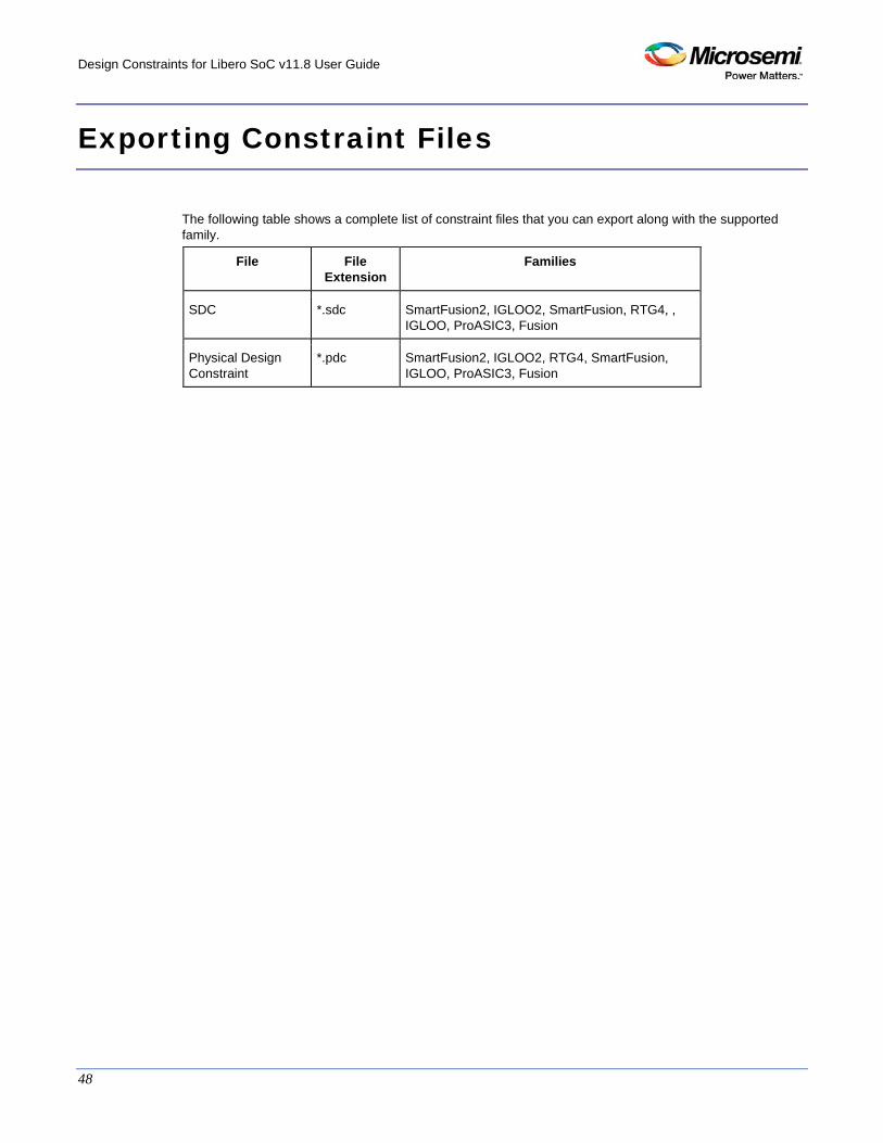
The following table shows a complete list of constraint files that you can export along with the supported family.
File File Extension
Families
SDC *.sdc SmartFusion2, IGLOO2, SmartFusion, RTG4, , IGLOO, ProASIC3, Fusion
Physical Design Constraint
*.pdc SmartFusion2, IGLOO2, RTG4, SmartFusion, IGLOO, ProASIC3, Fusion
Design Constraints for Libero SoC v11.8 User Guide
49
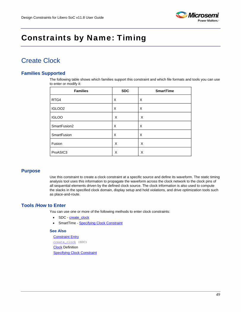
Constraints by Name: Timing
Create Clock
Families Supported The following table shows which families support this constraint and which file formats and tools you can use to enter or modify it:
Families SDC SmartTime
RTG4 X X
IGLOO2 X X
IGLOO X X
SmartFusion2 X X
SmartFusion X X
Fusion X X
ProASIC3 X X
Purpose Use this constraint to create a clock constraint at a specific source and define its waveform. The static timing analysis tool uses this information to propagate the waveform across the clock network to the clock pins of all sequential elements driven by the defined clock source. The clock information is also used to compute the slacks in the specified clock domain, display setup and hold violations, and drive optimization tools such as place-and-route.
Tools /How to Enter You can use one or more of the following methods to enter clock constraints:
• SDC - create_clock • SmartTime - Specifying Clock Constraint
See Also Constraint Entry create_clock (SDC)
Clock Definition Specifying Clock Constraint
Design Constraints for Libero SoC v11.8 User Guide
50
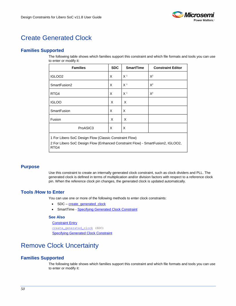
Create Generated Clock
Families Supported The following table shows which families support this constraint and which file formats and tools you can use to enter or modify it:
Families SDC SmartTime Constraint Editor
IGLOO2 X X 1 X2
SmartFusion2 X X 1 X2
RTG4 X X 1 X2
IGLOO X X
SmartFusion X X
Fusion X X
ProASIC3 X X
1 For Libero SoC Design Flow (Classic Constraint Flow) 2 For Libero SoC Design Flow (Enhanced Constraint Flow) - SmartFusion2, IGLOO2, RTG4
Purpose Use this constraint to create an internally generated clock constraint, such as clock dividers and PLL. The generated clock is defined in terms of multiplication and/or division factors with respect to a reference clock pin. When the reference clock pin changes, the generated clock is updated automatically.
Tools /How to Enter You can use one or more of the following methods to enter clock constraints: • SDC – create_generated_clock • SmartTime - Specifying Generated Clock Constraint
See Also Constraint Entry create_generated_clock (SDC)
Specifying Generated Clock Constraint
Remove Clock Uncertainty
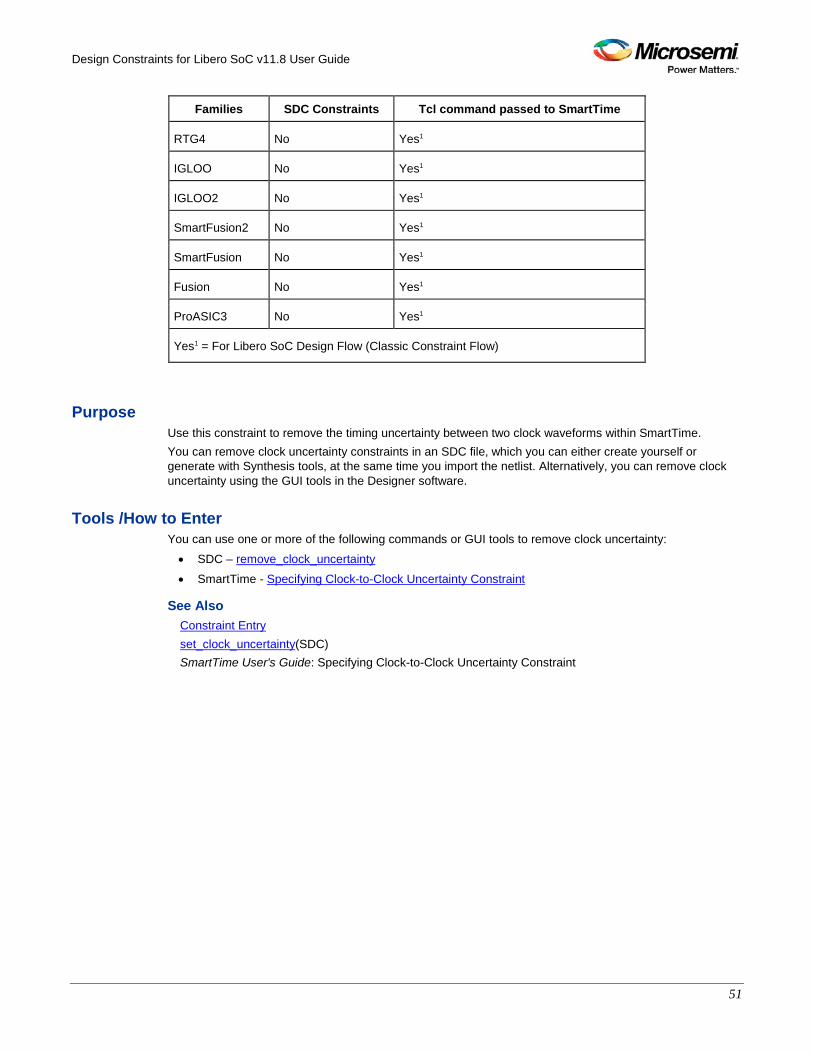
Families Supported The following table shows which families support this constraint and which file formats and tools you can use to enter or modify it:
Design Constraints for Libero SoC v11.8 User Guide
51
Families SDC Constraints Tcl command passed to SmartTime
RTG4 No Yes1
IGLOO No Yes1
IGLOO2 No Yes1
SmartFusion2 No Yes1
SmartFusion No Yes1
Fusion No Yes1
ProASIC3 No Yes1
Yes1 = For Libero SoC Design Flow (Classic Constraint Flow)
Purpose Use this constraint to remove the timing uncertainty between two clock waveforms within SmartTime. You can remove clock uncertainty constraints in an SDC file, which you can either create yourself or generate with Synthesis tools, at the same time you import the netlist. Alternatively, you can remove clock uncertainty using the GUI tools in the Designer software.
Tools /How to Enter You can use one or more of the following commands or GUI tools to remove clock uncertainty:
• SDC – remove_clock_uncertainty
• SmartTime - Specifying Clock-to-Clock Uncertainty Constraint
See Also Constraint Entry set_clock_uncertainty(SDC) SmartTime User's Guide: Specifying Clock-to-Clock Uncertainty Constraint
Design Constraints for Libero SoC v11.8 User Guide
52
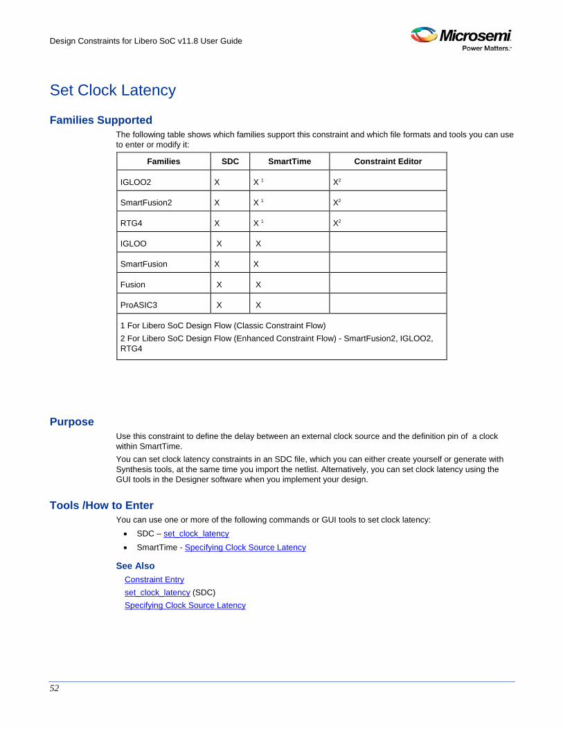
Set Clock Latency
Families Supported The following table shows which families support this constraint and which file formats and tools you can use to enter or modify it:
Families SDC SmartTime Constraint Editor
IGLOO2 X X 1 X2
SmartFusion2 X X 1 X2
RTG4 X X 1 X2
IGLOO X X
SmartFusion X X
Fusion X X
ProASIC3 X X
1 For Libero SoC Design Flow (Classic Constraint Flow) 2 For Libero SoC Design Flow (Enhanced Constraint Flow) - SmartFusion2, IGLOO2, RTG4
Purpose Use this constraint to define the delay between an external clock source and the definition pin of a clock within SmartTime. You can set clock latency constraints in an SDC file, which you can either create yourself or generate with Synthesis tools, at the same time you import the netlist. Alternatively, you can set clock latency using the GUI tools in the Designer software when you implement your design.
Tools /How to Enter You can use one or more of the following commands or GUI tools to set clock latency:
• SDC – set_clock_latency
• SmartTime - Specifying Clock Source Latency
See Also Constraint Entry set_clock_latency (SDC) Specifying Clock Source Latency
Design Constraints for Libero SoC v11.8 User Guide
53
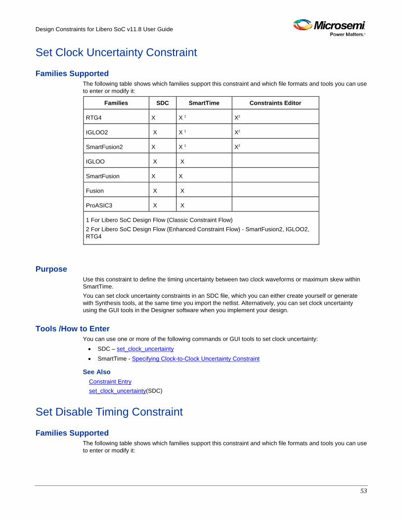
Set Clock Uncertainty Constraint
Families Supported The following table shows which families support this constraint and which file formats and tools you can use to enter or modify it:
Families SDC SmartTime Constraints Editor
RTG4 X X 1 X2
IGLOO2 X X 1 X2
SmartFusion2 X X 1 X2
IGLOO X X
SmartFusion X X
Fusion X X
ProASIC3 X X
1 For Libero SoC Design Flow (Classic Constraint Flow) 2 For Libero SoC Design Flow (Enhanced Constraint Flow) - SmartFusion2, IGLOO2, RTG4
Purpose Use this constraint to define the timing uncertainty between two clock waveforms or maximum skew within SmartTime. You can set clock uncertainty constraints in an SDC file, which you can either create yourself or generate with Synthesis tools, at the same time you import the netlist. Alternatively, you can set clock uncertainty using the GUI tools in the Designer software when you implement your design.
Tools /How to Enter You can use one or more of the following commands or GUI tools to set clock uncertainty:
• SDC – set_clock_uncertainty
• SmartTime - Specifying Clock-to-Clock Uncertainty Constraint
See Also Constraint Entry set_clock_uncertainty(SDC)
Set Disable Timing Constraint
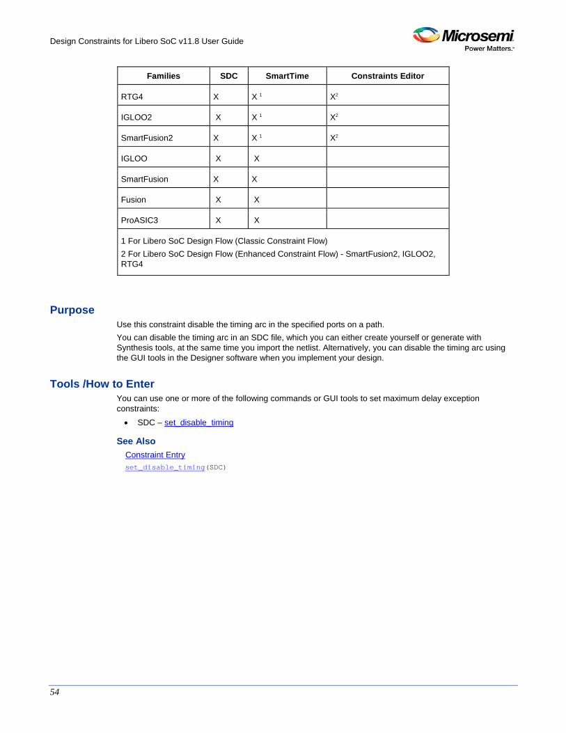
Families Supported The following table shows which families support this constraint and which file formats and tools you can use to enter or modify it:
Design Constraints for Libero SoC v11.8 User Guide
54
Families SDC SmartTime Constraints Editor
RTG4 X X 1 X2
IGLOO2 X X 1 X2
SmartFusion2 X X 1 X2
IGLOO X X
SmartFusion X X
Fusion X X
ProASIC3 X X
1 For Libero SoC Design Flow (Classic Constraint Flow) 2 For Libero SoC Design Flow (Enhanced Constraint Flow) - SmartFusion2, IGLOO2, RTG4
Purpose Use this constraint disable the timing arc in the specified ports on a path. You can disable the timing arc in an SDC file, which you can either create yourself or generate with Synthesis tools, at the same time you import the netlist. Alternatively, you can disable the timing arc using the GUI tools in the Designer software when you implement your design.
Tools /How to Enter You can use one or more of the following commands or GUI tools to set maximum delay exception constraints:
• SDC – set_disable_timing
See Also Constraint Entry set_disable_timing(SDC)
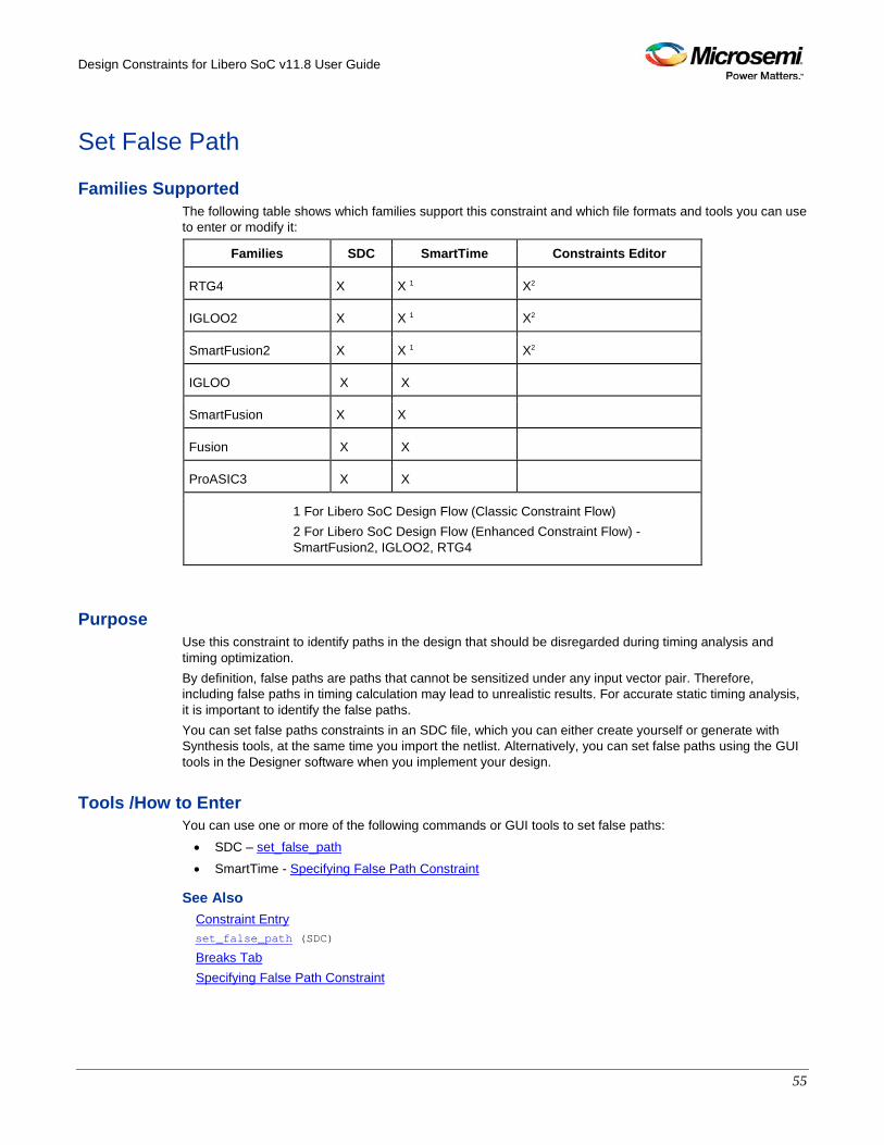
Design Constraints for Libero SoC v11.8 User Guide
55
Set False Path
Families Supported The following table shows which families support this constraint and which file formats and tools you can use to enter or modify it:
Families SDC SmartTime Constraints Editor
RTG4 X X 1 X2
IGLOO2 X X 1 X2
SmartFusion2 X X 1 X2
IGLOO X X
SmartFusion X X
Fusion X X
ProASIC3 X X
1 For Libero SoC Design Flow (Classic Constraint Flow) 2 For Libero SoC Design Flow (Enhanced Constraint Flow) - SmartFusion2, IGLOO2, RTG4
Purpose Use this constraint to identify paths in the design that should be disregarded during timing analysis and timing optimization. By definition, false paths are paths that cannot be sensitized under any input vector pair. Therefore, including false paths in timing calculation may lead to unrealistic results. For accurate static timing analysis, it is important to identify the false paths. You can set false paths constraints in an SDC file, which you can either create yourself or generate with Synthesis tools, at the same time you import the netlist. Alternatively, you can set false paths using the GUI tools in the Designer software when you implement your design.
Tools /How to Enter You can use one or more of the following commands or GUI tools to set false paths:
• SDC – set_false_path
• SmartTime - Specifying False Path Constraint
See Also Constraint Entry set_false_path (SDC)
Breaks Tab Specifying False Path Constraint
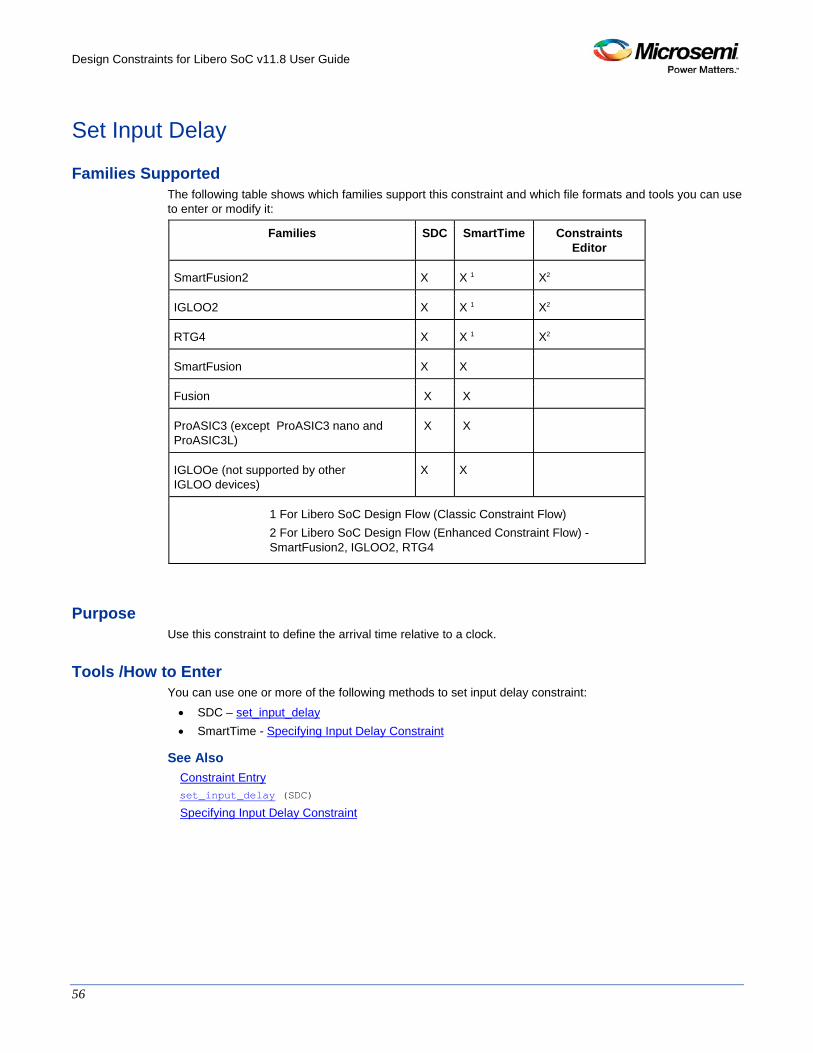
Design Constraints for Libero SoC v11.8 User Guide
56
Set Input Delay
Families Supported The following table shows which families support this constraint and which file formats and tools you can use to enter or modify it:
Families SDC SmartTime Constraints Editor
SmartFusion2 X X 1 X2
IGLOO2 X X 1 X2
RTG4 X X 1 X2
SmartFusion X X
Fusion X X
ProASIC3 (except ProASIC3 nano and ProASIC3L)
X X
IGLOOe (not supported by other IGLOO devices)
X X
1 For Libero SoC Design Flow (Classic Constraint Flow) 2 For Libero SoC Design Flow (Enhanced Constraint Flow) - SmartFusion2, IGLOO2, RTG4
Purpose Use this constraint to define the arrival time relative to a clock.
Tools /How to Enter You can use one or more of the following methods to set input delay constraint:
• SDC – set_input_delay • SmartTime - Specifying Input Delay Constraint
See Also Constraint Entry set_input_delay (SDC)
Specifying Input Delay Constraint
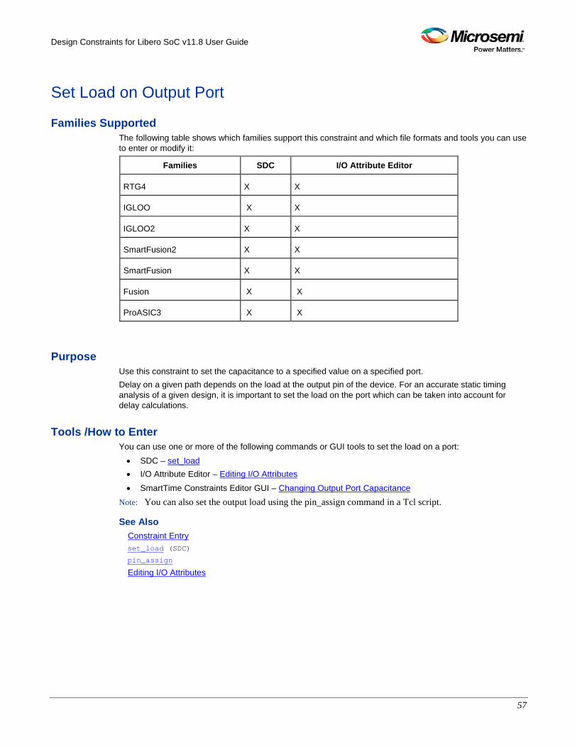
Design Constraints for Libero SoC v11.8 User Guide
57
Set Load on Output Port
Families Supported The following table shows which families support this constraint and which file formats and tools you can use to enter or modify it:
Families SDC I/O Attribute Editor
RTG4 X X
IGLOO X X
IGLOO2 X X
SmartFusion2 X X
SmartFusion X X
Fusion X X
ProASIC3 X X
Purpose Use this constraint to set the capacitance to a specified value on a specified port. Delay on a given path depends on the load at the output pin of the device. For an accurate static timing analysis of a given design, it is important to set the load on the port which can be taken into account for delay calculations.
Tools /How to Enter You can use one or more of the following commands or GUI tools to set the load on a port:
• SDC – set_load • I/O Attribute Editor – Editing I/O Attributes • SmartTime Constraints Editor GUI – Changing Output Port Capacitance
Note: You can also set the output load using the pin_assign command in a Tcl script.
See Also Constraint Entry set_load (SDC)
pin_assign
Editing I/O Attributes
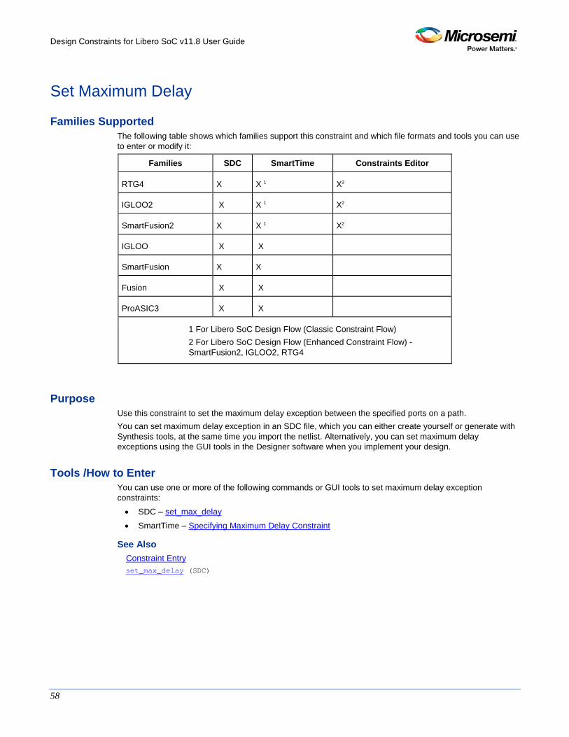
Design Constraints for Libero SoC v11.8 User Guide
58
Set Maximum Delay
Families Supported The following table shows which families support this constraint and which file formats and tools you can use to enter or modify it:
Families SDC SmartTime Constraints Editor
RTG4 X X 1 X2
IGLOO2 X X 1 X2
SmartFusion2 X X 1 X2
IGLOO X X
SmartFusion X X
Fusion X X
ProASIC3 X X
1 For Libero SoC Design Flow (Classic Constraint Flow) 2 For Libero SoC Design Flow (Enhanced Constraint Flow) - SmartFusion2, IGLOO2, RTG4
Purpose Use this constraint to set the maximum delay exception between the specified ports on a path. You can set maximum delay exception in an SDC file, which you can either create yourself or generate with Synthesis tools, at the same time you import the netlist. Alternatively, you can set maximum delay exceptions using the GUI tools in the Designer software when you implement your design.
Tools /How to Enter You can use one or more of the following commands or GUI tools to set maximum delay exception constraints:
• SDC – set_max_delay
• SmartTime – Specifying Maximum Delay Constraint
See Also Constraint Entry set_max_delay (SDC)
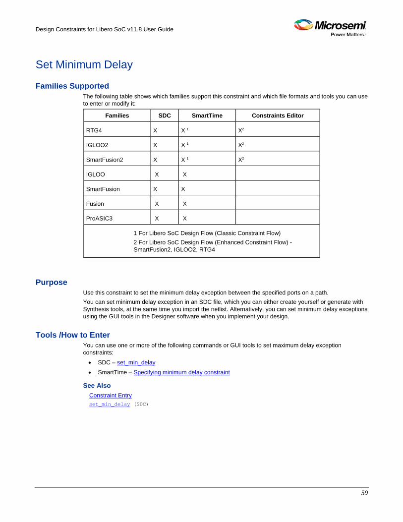
Design Constraints for Libero SoC v11.8 User Guide
59
Set Minimum Delay
Families Supported The following table shows which families support this constraint and which file formats and tools you can use to enter or modify it:
Families SDC SmartTime Constraints Editor
RTG4 X X 1 X2
IGLOO2 X X 1 X2
SmartFusion2 X X 1 X2
IGLOO X X
SmartFusion X X
Fusion X X
ProASIC3 X X
1 For Libero SoC Design Flow (Classic Constraint Flow) 2 For Libero SoC Design Flow (Enhanced Constraint Flow) - SmartFusion2, IGLOO2, RTG4
Purpose Use this constraint to set the minimum delay exception between the specified ports on a path. You can set minimum delay exception in an SDC file, which you can either create yourself or generate with Synthesis tools, at the same time you import the netlist. Alternatively, you can set minimum delay exceptions using the GUI tools in the Designer software when you implement your design.
Tools /How to Enter You can use one or more of the following commands or GUI tools to set maximum delay exception constraints:
• SDC – set_min_delay
• SmartTime – Specifying minimum delay constraint
See Also Constraint Entry set_min_delay (SDC)
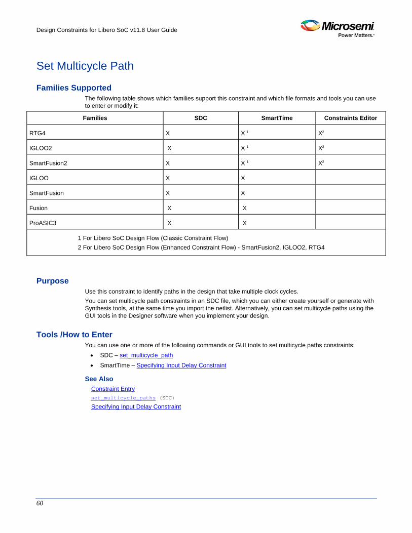
Design Constraints for Libero SoC v11.8 User Guide
60
Set Multicycle Path
Families Supported The following table shows which families support this constraint and which file formats and tools you can use to enter or modify it:
Families SDC SmartTime Constraints Editor
RTG4 X X 1 X2
IGLOO2 X X 1 X2
SmartFusion2 X X 1 X2
IGLOO X X
SmartFusion X X
Fusion X X
ProASIC3 X X
1 For Libero SoC Design Flow (Classic Constraint Flow) 2 For Libero SoC Design Flow (Enhanced Constraint Flow) - SmartFusion2, IGLOO2, RTG4
Purpose Use this constraint to identify paths in the design that take multiple clock cycles. You can set multicycle path constraints in an SDC file, which you can either create yourself or generate with Synthesis tools, at the same time you import the netlist. Alternatively, you can set multicycle paths using the GUI tools in the Designer software when you implement your design.
Tools /How to Enter You can use one or more of the following commands or GUI tools to set multicycle paths constraints: • SDC – set_multicycle_path
• SmartTime – Specifying Input Delay Constraint
See Also Constraint Entry set_multicycle_paths (SDC)
Specifying Input Delay Constraint
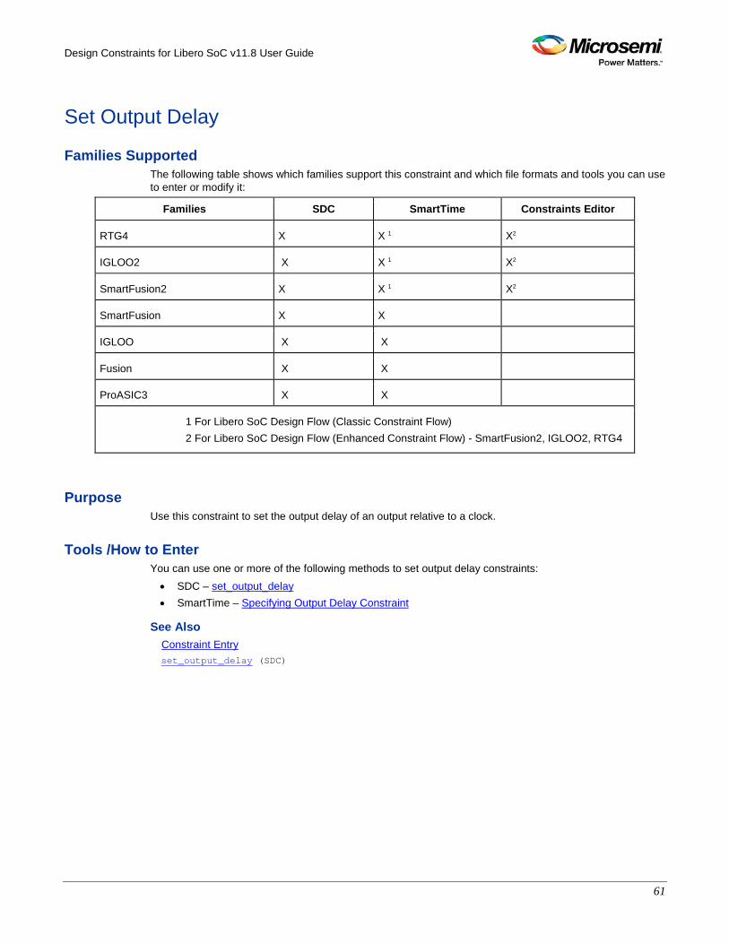
Design Constraints for Libero SoC v11.8 User Guide
61
Set Output Delay
Families Supported The following table shows which families support this constraint and which file formats and tools you can use to enter or modify it:
Families SDC SmartTime Constraints Editor
RTG4 X X 1 X2
IGLOO2 X X 1 X2
SmartFusion2 X X 1 X2
SmartFusion X X
IGLOO X X
Fusion X X
ProASIC3 X X
1 For Libero SoC Design Flow (Classic Constraint Flow) 2 For Libero SoC Design Flow (Enhanced Constraint Flow) - SmartFusion2, IGLOO2, RTG4
Purpose Use this constraint to set the output delay of an output relative to a clock.
Tools /How to Enter You can use one or more of the following methods to set output delay constraints: • SDC – set_output_delay • SmartTime – Specifying Output Delay Constraint
See Also Constraint Entry set_output_delay (SDC)

Design Constraints for Libero SoC v11.8 User Guide
62
Constraints by Name: Physical
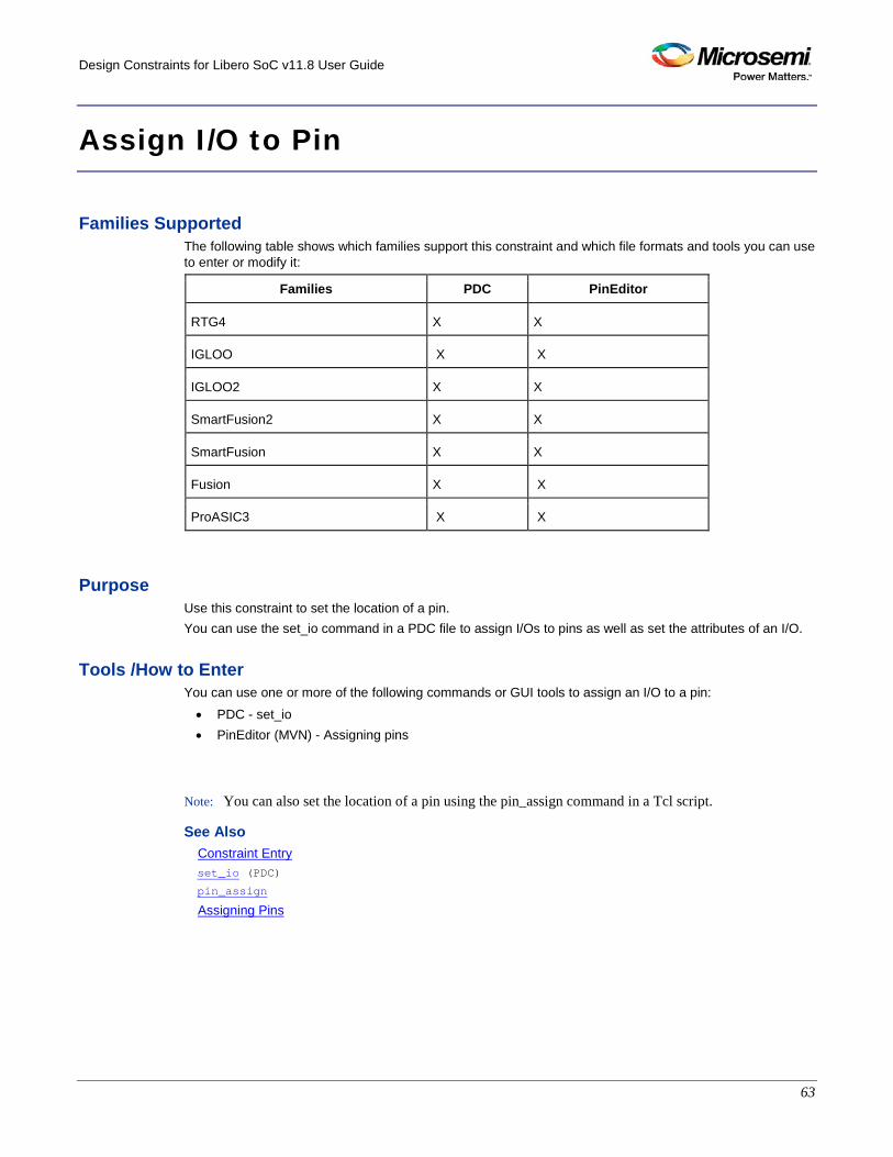
Design Constraints for Libero SoC v11.8 User Guide
63
Assign I/O to Pin
Families Supported The following table shows which families support this constraint and which file formats and tools you can use to enter or modify it:
Families PDC PinEditor
RTG4 X X
IGLOO X X
IGLOO2 X X
SmartFusion2 X X
SmartFusion X X
Fusion X X
ProASIC3 X X
Purpose Use this constraint to set the location of a pin. You can use the set_io command in a PDC file to assign I/Os to pins as well as set the attributes of an I/O.
Tools /How to Enter You can use one or more of the following commands or GUI tools to assign an I/O to a pin:
• PDC - set_io • PinEditor (MVN) - Assigning pins
Note: You can also set the location of a pin using the pin_assign command in a Tcl script.
See Also Constraint Entry set_io (PDC)
pin_assign
Assigning Pins
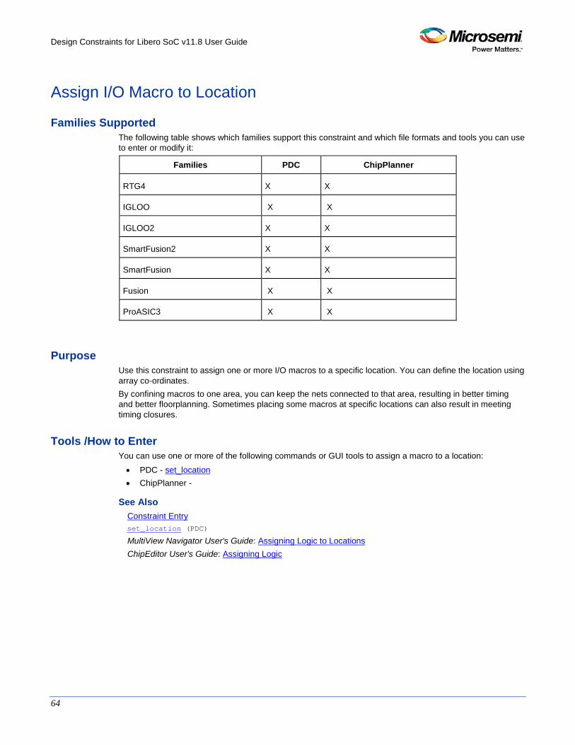
Design Constraints for Libero SoC v11.8 User Guide
64
Assign I/O Macro to Location
Families Supported The following table shows which families support this constraint and which file formats and tools you can use to enter or modify it:
Families PDC ChipPlanner
RTG4 X X
IGLOO X X
IGLOO2 X X
SmartFusion2 X X
SmartFusion X X
Fusion X X
ProASIC3 X X
Purpose Use this constraint to assign one or more I/O macros to a specific location. You can define the location using array co-ordinates. By confining macros to one area, you can keep the nets connected to that area, resulting in better timing and better floorplanning. Sometimes placing some macros at specific locations can also result in meeting timing closures.
Tools /How to Enter You can use one or more of the following commands or GUI tools to assign a macro to a location:
• PDC - set_location • ChipPlanner -
See Also Constraint Entry set_location (PDC)
MultiView Navigator User's Guide: Assigning Logic to Locations ChipEditor User's Guide: Assigning Logic
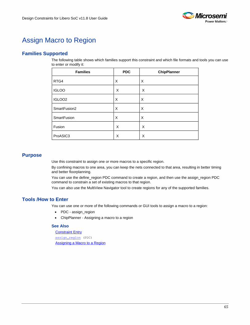
Design Constraints for Libero SoC v11.8 User Guide
65
Assign Macro to Region
Families Supported The following table shows which families support this constraint and which file formats and tools you can use to enter or modify it:
Families PDC ChipPlanner
RTG4 X X
IGLOO X X
IGLOO2 X X
SmartFusion2 X X
SmartFusion X X
Fusion X X
ProASIC3 X X
Purpose Use this constraint to assign one or more macros to a specific region. By confining macros to one area, you can keep the nets connected to that area, resulting in better timing and better floorplanning. You can use the define_region PDC command to create a region, and then use the assign_region PDC command to constrain a set of existing macros to that region. You can also use the MultiView Navigator tool to create regions for any of the supported families.
Tools /How to Enter You can use one or more of the following commands or GUI tools to assign a macro to a region: • PDC - assign_region • ChipPlanner - Assigning a macro to a region
See Also Constraint Entry assign_region (PDC)
Assigning a Macro to a Region
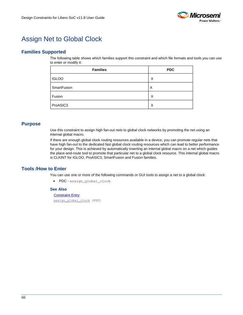
Design Constraints for Libero SoC v11.8 User Guide
66
Assign Net to Global Clock
Families Supported The following table shows which families support this constraint and which file formats and tools you can use to enter or modify it:
Families PDC
IGLOO X
SmartFusion X
Fusion X
ProASIC3 X
Purpose Use this constraint to assign high fan-out nets to global clock networks by promoting the net using an internal global macro. If there are enough global clock routing resources available in a device, you can promote regular nets that have high fan-out to the dedicated fast global clock routing resources which can lead to better performance for your design. This is achieved by automatically inserting an internal global macro on a net which guides the place-and-route tool to promote that particular net to a global clock resource. This internal global macro is CLKINT for IGLOO, ProASIC3, SmartFusion and Fusion families.
Tools /How to Enter You can use one or more of the following commands or GUI tools to assign a net to a global clock:
• PDC - assign_global_clock
See Also Constraint Entry assign_global_clock (PDC)
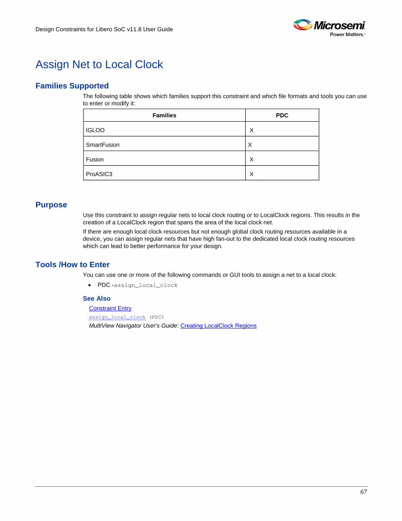
Design Constraints for Libero SoC v11.8 User Guide
67
Assign Net to Local Clock
Families Supported The following table shows which families support this constraint and which file formats and tools you can use to enter or modify it:
Families PDC
IGLOO X
SmartFusion X
Fusion X
ProASIC3 X
Purpose Use this constraint to assign regular nets to local clock routing or to LocalClock regions. This results in the creation of a LocalClock region that spans the area of the local clock net. If there are enough local clock resources but not enough global clock routing resources available in a device, you can assign regular nets that have high fan-out to the dedicated local clock routing resources which can lead to better performance for your design.
Tools /How to Enter You can use one or more of the following commands or GUI tools to assign a net to a local clock:
• PDC -assign_local_clock
See Also Constraint Entry assign_local_clock (PDC)
MultiView Navigator User's Guide: Creating LocalClock Regions

Design Constraints for Libero SoC v11.8 User Guide
68
Assign Net to Quadrant Clock
Families Supported The following table shows which families support this constraint and which file formats and tools you can use to enter or modify it:
Families PDC ChipPlanner
IGLOO X X
SmartFusion X X
Fusion X X
ProASIC3 X X
Purpose Use this constraint to assign regular nets to quadrant clock routing. This results in the creation of a QuadrantClock region that spans the area of the quadrant clock net. If there are enough quadrant clock resources but not enough global clock routing resources available in a device, you can promote regular nets that have high fan-out to the dedicated quadrant clock routing resources which can lead to better performance for your design.
Tools /How to Enter You can use one or more of the following commands or GUI tools to assign a net to a local clock:
• PDC - assign_quadrant_clock
• ChipPlanner - Creating QuadrantClock Regions
See Also Constraint Entry assign_quadrant_clock (PDC)
MultiView Navigator User's Guide: Creating QuadrantClock Regions
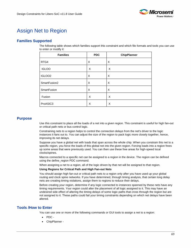
Design Constraints for Libero SoC v11.8 User Guide
69
Assign Net to Region
Families Supported The following table shows which families support this constraint and which file formats and tools you can use to enter or modify it:
Families PDC ChipPlanner
RTG4 X X
IGLOO X X
IGLOO2 X X
SmartFusion2 X X
SmartFusion X X
Fusion X X
ProASIC3 X X
Purpose Use this constraint to place all the loads of a net into a given region. This constraint is useful for high fan-out or critical path nets or bus control logic. Constraining nets to a region helps to control the connection delays from the net's driver to the logic instances it fans out to. You can adjust the size of the region to pack logic more closely together, hence, improving its net delays. Suppose you have a global net with loads that span across the whole chip. When you constrain this net to a specific region, you force the loads of this global net into the given region. Forcing loads into a region frees up some areas that were previously used. You can then use these free areas for high-speed local clocks/spines. Macros connected to a specific net can be assigned to a region in the device. The region can be defined using the define_region PDC command. When assigning a net to a region, all of the logic driven by that net will be assigned to that region. Using Regions for Critical Path and High Fan-out Nets You should assign high fan-out or critical path nets to a region only after you have used up your global routing and clock spine networks. If you have determined, through timing analysis, that certain long delay nets are creating timing violations, assign them to regions to reduce their delays. Before creating your region, determine if any logic connected to instances spanned by these nets have any timing requirements. Your region could alter the placement of all logic assigned to it. This may have an undesired side effect of altering the timing delays of some logic paths that cross through the region but are not assigned to it. These paths could fail your timing constraints depending on which net delays have been altered.
Tools /How to Enter You can use one or more of the following commands or GUI tools to assign a net to a region: • PDC - • ChipPlanner -
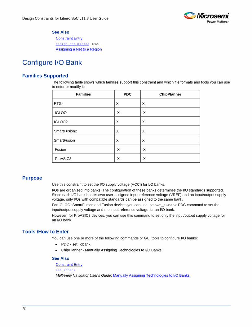
Design Constraints for Libero SoC v11.8 User Guide
70
See Also Constraint Entry assign_net_macros (PDC)
Assigning a Net to a Region
Configure I/O Bank
Families Supported The following table shows which families support this constraint and which file formats and tools you can use to enter or modify it:
Families PDC ChipPlanner
RTG4 X X
IGLOO X X
IGLOO2 X X
SmartFusion2 X X
SmartFusion X X
Fusion X X
ProASIC3 X X
Purpose Use this constraint to set the I/O supply voltage (VCCI) for I/O banks. I/Os are organized into banks. The configuration of these banks determines the I/O standards supported. Since each I/O bank has its own user-assigned input reference voltage (VREF) and an input/output supply voltage, only I/Os with compatible standards can be assigned to the same bank. For IGLOO, SmartFusion and Fusion devices you can use the set_iobank PDC command to set the input/output supply voltage and the input reference voltage for an I/O bank. However, for ProASIC3 devices, you can use this command to set only the input/output supply voltage for an I/O bank.
Tools /How to Enter You can use one or more of the following commands or GUI tools to configure I/O banks: • PDC - set_iobank • ChipPlanner - Manually Assigning Technologies to I/O Banks
See Also Constraint Entry set_iobank
MultiView Navigator User's Guide: Manually Assigning Technologies to I/O Banks
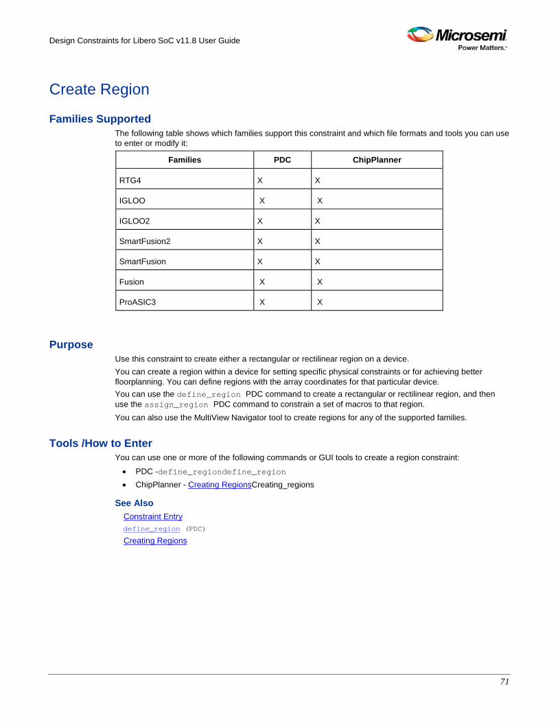
Design Constraints for Libero SoC v11.8 User Guide
71
Create Region
Families Supported The following table shows which families support this constraint and which file formats and tools you can use to enter or modify it:
Families PDC ChipPlanner
RTG4 X X
IGLOO X X
IGLOO2 X X
SmartFusion2 X X
SmartFusion X X
Fusion X X
ProASIC3 X X
Purpose Use this constraint to create either a rectangular or rectilinear region on a device. You can create a region within a device for setting specific physical constraints or for achieving better floorplanning. You can define regions with the array coordinates for that particular device. You can use the define_region PDC command to create a rectangular or rectilinear region, and then use the assign_region PDC command to constrain a set of macros to that region. You can also use the MultiView Navigator tool to create regions for any of the supported families.
Tools /How to Enter You can use one or more of the following commands or GUI tools to create a region constraint:
• PDC -define_regiondefine_region • ChipPlanner - Creating RegionsCreating_regions
See Also Constraint Entry define_region (PDC)
Creating Regions
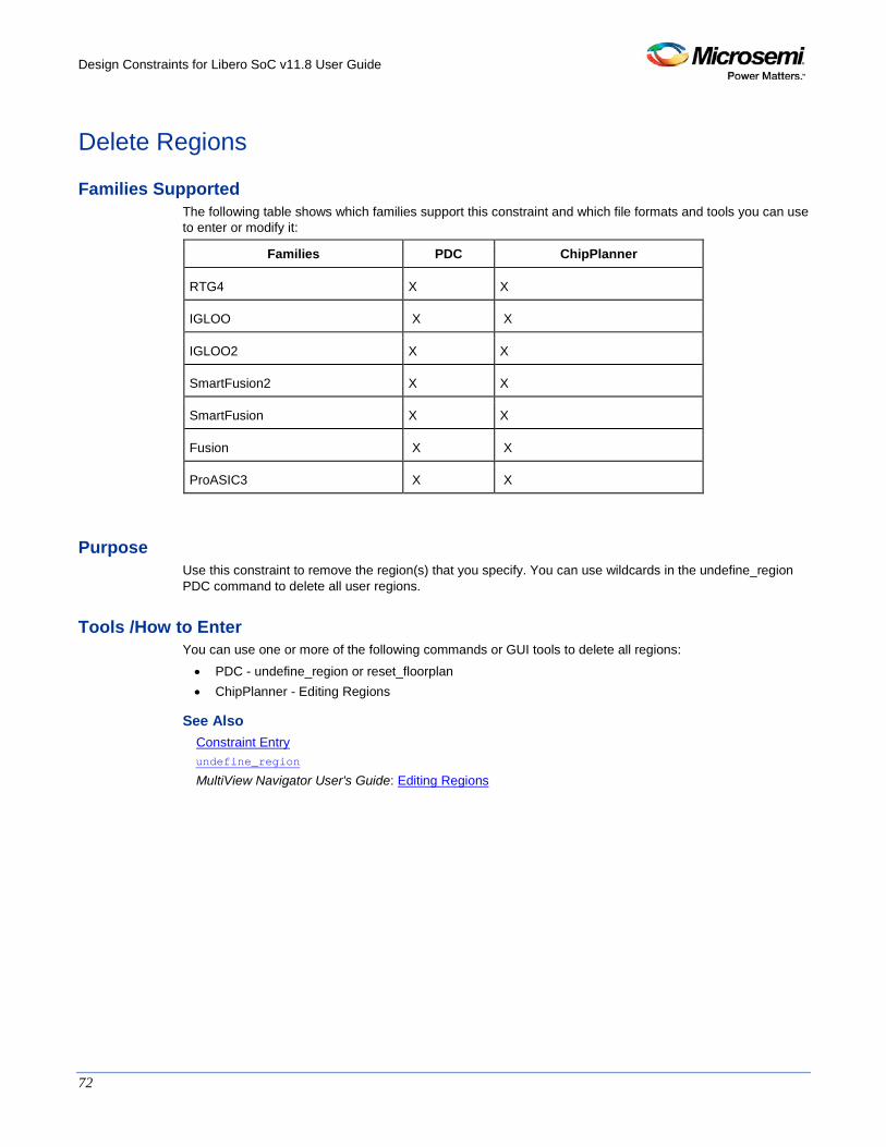
Design Constraints for Libero SoC v11.8 User Guide
72
Delete Regions
Families Supported The following table shows which families support this constraint and which file formats and tools you can use to enter or modify it:
Families PDC ChipPlanner
RTG4 X X
IGLOO X X
IGLOO2 X X
SmartFusion2 X X
SmartFusion X X
Fusion X X
ProASIC3 X X
Purpose Use this constraint to remove the region(s) that you specify. You can use wildcards in the undefine_region PDC command to delete all user regions.
Tools /How to Enter You can use one or more of the following commands or GUI tools to delete all regions:
• PDC - undefine_region or reset_floorplan • ChipPlanner - Editing Regions
See Also Constraint Entry undefine_region
MultiView Navigator User's Guide: Editing Regions
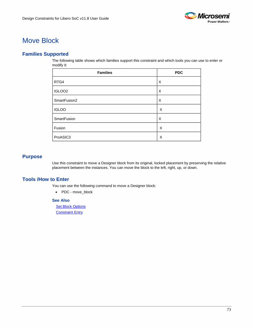
Design Constraints for Libero SoC v11.8 User Guide
73
Move Block
Families Supported The following table shows which families support this constraint and which tools you can use to enter or modify it:
Families PDC
RTG4 X
IGLOO2 X
SmartFusion2 X
IGLOO X
SmartFusion X
Fusion X
ProASIC3 X
Purpose Use this constraint to move a Designer block from its original, locked placement by preserving the relative placement between the instances. You can move the block to the left, right, up, or down.
Tools /How to Enter You can use the following command to move a Designer block:
• PDC - move_block
See Also Set Block Options Constraint Entry
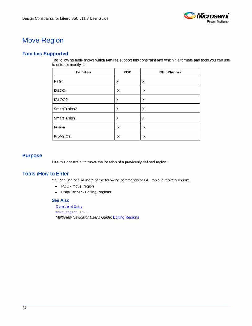
Design Constraints for Libero SoC v11.8 User Guide
74
Move Region
Families Supported The following table shows which families support this constraint and which file formats and tools you can use to enter or modify it:
Families PDC ChipPlanner
RTG4 X X
IGLOO X X
IGLOO2 X X
SmartFusion2 X X
SmartFusion X X
Fusion X X
ProASIC3 X X
Purpose Use this constraint to move the location of a previously defined region.
Tools /How to Enter You can use one or more of the following commands or GUI tools to move a region:
• PDC - move_region • ChipPlanner - Editing Regions
See Also Constraint Entry move_region (PDC)
MultiView Navigator User's Guide: Editing Regions
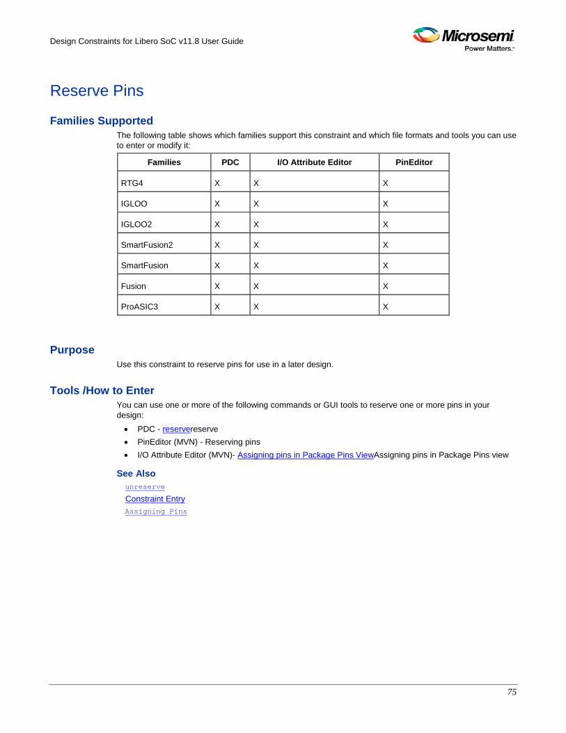
Design Constraints for Libero SoC v11.8 User Guide
75
Reserve Pins
Families Supported The following table shows which families support this constraint and which file formats and tools you can use to enter or modify it:
Families PDC I/O Attribute Editor PinEditor
RTG4 X X X
IGLOO X X X
IGLOO2 X X X
SmartFusion2 X X X
SmartFusion X X X
Fusion X X X
ProASIC3 X X X
Purpose Use this constraint to reserve pins for use in a later design.
Tools /How to Enter You can use one or more of the following commands or GUI tools to reserve one or more pins in your design:
• PDC - reservereserve • PinEditor (MVN) - Reserving pins • I/O Attribute Editor (MVN)- Assigning pins in Package Pins ViewAssigning pins in Package Pins view
See Also unreserve
Constraint Entry Assigning Pins
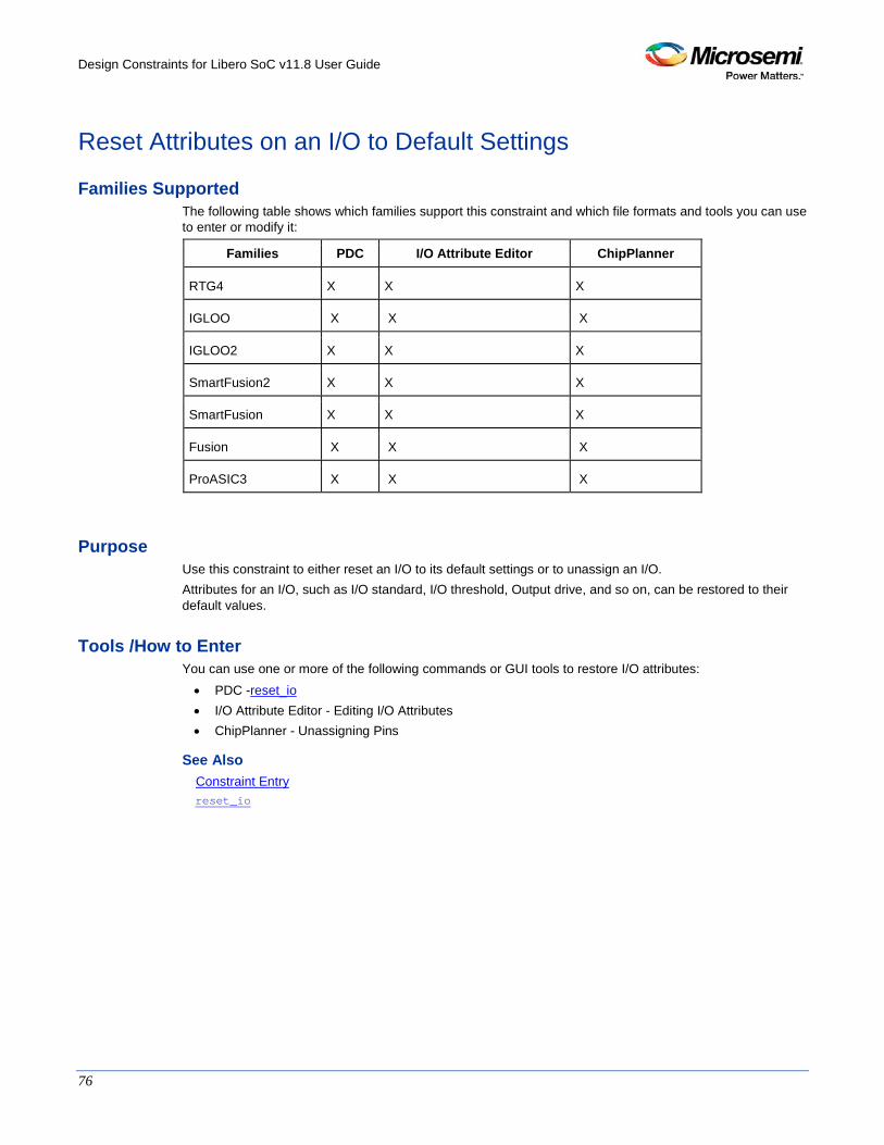
Design Constraints for Libero SoC v11.8 User Guide
76
Reset Attributes on an I/O to Default Settings
Families Supported The following table shows which families support this constraint and which file formats and tools you can use to enter or modify it:
Families PDC I/O Attribute Editor ChipPlanner
RTG4 X X X
IGLOO X X X
IGLOO2 X X X
SmartFusion2 X X X
SmartFusion X X X
Fusion X X X
ProASIC3 X X X
Purpose Use this constraint to either reset an I/O to its default settings or to unassign an I/O. Attributes for an I/O, such as I/O standard, I/O threshold, Output drive, and so on, can be restored to their default values.
Tools /How to Enter You can use one or more of the following commands or GUI tools to restore I/O attributes: • PDC -reset_io • I/O Attribute Editor - Editing I/O Attributes • ChipPlanner - Unassigning Pins
See Also Constraint Entry reset_io
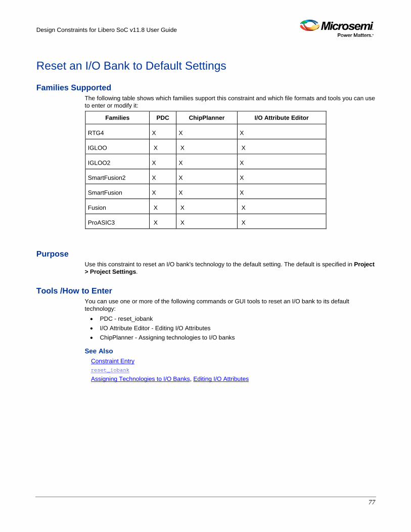
Design Constraints for Libero SoC v11.8 User Guide
77
Reset an I/O Bank to Default Settings
Families Supported The following table shows which families support this constraint and which file formats and tools you can use to enter or modify it:
Families PDC ChipPlanner I/O Attribute Editor
RTG4 X X X
IGLOO X X X
IGLOO2 X X X
SmartFusion2 X X X
SmartFusion X X X
Fusion X X X
ProASIC3 X X X
Purpose Use this constraint to reset an I/O bank's technology to the default setting. The default is specified in Project > Project Settings.
Tools /How to Enter You can use one or more of the following commands or GUI tools to reset an I/O bank to its default technology: • PDC - reset_iobank • I/O Attribute Editor - Editing I/O Attributes • ChipPlanner - Assigning technologies to I/O banks
See Also Constraint Entry reset_iobank
Assigning Technologies to I/O Banks, Editing I/O Attributes
Design Constraints for Libero SoC v11.8 User Guide
78
Reset Net's Criticality to Default Level
Families Supported The following table shows which families support this constraint and which file formats and tools you can use to enter or modify it:
Families PDC
IGLOO X
SmartFusion X
Fusion X
ProASIC3 X
Purpose Use this constraint to reset a net's criticality to its default value, which is 5. Net criticality is a guide for the place-and-route tool to keep instances connected to a net as close as possible, at the cost of other (less critical) nets. Net criticality can vary from 1 to 10 with 1 being the least critical and 10 being the most.
Tools /How to Enter You can use one or more of the following commands or GUI tools to reset net criticality:
• PDC - reset_net_critical
See Also Constraint Entry reset_net_critical
set_net_critical
Design Constraints for Libero SoC v11.8 User Guide
79
Set Block Options
Families Supported The following table shows which families support this constraint and which tools you can use to enter or modify it:
Families PDC
RTG4 X
IGLOO2 X
SmartFusion2 X
IGLOO X
SmartFusion X
Fusion X
ProASIC3 X
Purpose Use this constraint to override the compile option for placement or routing conflicts for an instance of a Designer block.
Tools /How to Enter You can use the following command to preserve instances:
• PDC - set_block_options
See Also Move Block Constraint Entry
Design Constraints for Libero SoC v11.8 User Guide
80
Set Net's Criticality
Families Supported The following table shows which families support this constraint and which file formats and tools you can use to enter or modify it:
Families PDC
IGLOO X
SmartFusion X
Fusion X
ProASIC3 X
Purpose Use this constraint to set the level at which the place-and-route tool must keep instances connected to a net. Net criticality is a guide for the place-and-route tool to keep instances connected to a net as close as possible at the cost of other (less critical) nets. Net criticality can vary from 1 to 10 with 1 being the least critical and 10 being the most. You can set a net's criticality to any number between 1 and 10 to help place-and-route tool prioritize its timing driven placement.
Tools /How to Enter set_net_critical
See Also Constraint Entry set_net_critical
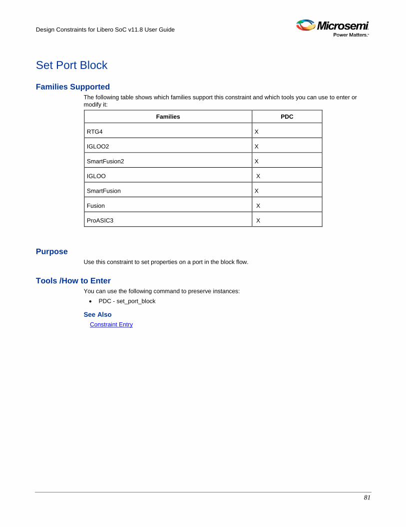
Design Constraints for Libero SoC v11.8 User Guide
81
Set Port Block
Families Supported The following table shows which families support this constraint and which tools you can use to enter or modify it:
Families PDC
RTG4 X
IGLOO2 X
SmartFusion2 X
IGLOO X
SmartFusion X
Fusion X
ProASIC3 X
Purpose Use this constraint to set properties on a port in the block flow.
Tools /How to Enter You can use the following command to preserve instances:
• PDC - set_port_block
See Also Constraint Entry
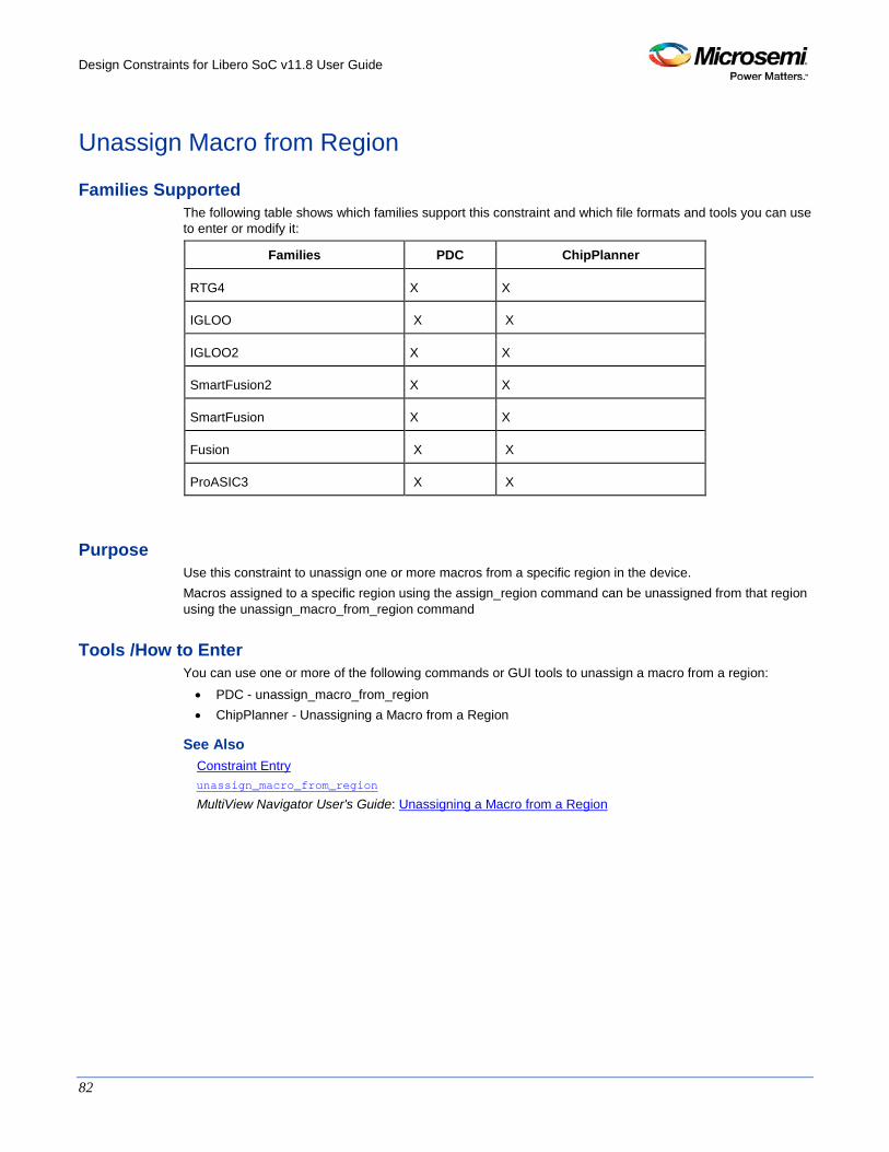
Design Constraints for Libero SoC v11.8 User Guide
82
Unassign Macro from Region
Families Supported The following table shows which families support this constraint and which file formats and tools you can use to enter or modify it:
Families PDC ChipPlanner
RTG4 X X
IGLOO X X
IGLOO2 X X
SmartFusion2 X X
SmartFusion X X
Fusion X X
ProASIC3 X X
Purpose Use this constraint to unassign one or more macros from a specific region in the device. Macros assigned to a specific region using the assign_region command can be unassigned from that region using the unassign_macro_from_region command
Tools /How to Enter You can use one or more of the following commands or GUI tools to unassign a macro from a region: • PDC - unassign_macro_from_region • ChipPlanner - Unassigning a Macro from a Region
See Also Constraint Entry unassign_macro_from_region
MultiView Navigator User's Guide: Unassigning a Macro from a Region
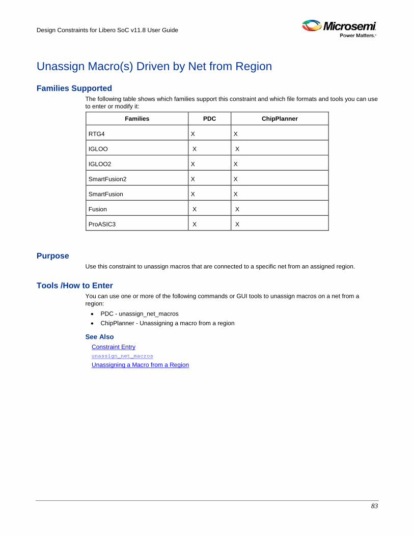
Design Constraints for Libero SoC v11.8 User Guide
83
Unassign Macro(s) Driven by Net from Region
Families Supported The following table shows which families support this constraint and which file formats and tools you can use to enter or modify it:
Families PDC ChipPlanner
RTG4 X X
IGLOO X X
IGLOO2 X X
SmartFusion2 X X
SmartFusion X X
Fusion X X
ProASIC3 X X
Purpose Use this constraint to unassign macros that are connected to a specific net from an assigned region.
Tools /How to Enter You can use one or more of the following commands or GUI tools to unassign macros on a net from a region:
• PDC - unassign_net_macros • ChipPlanner - Unassigning a macro from a region
See Also Constraint Entry unassign_net_macros
Unassigning a Macro from a Region
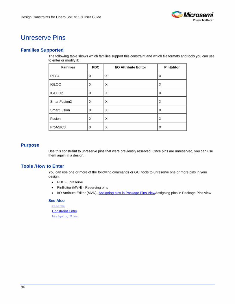
Design Constraints for Libero SoC v11.8 User Guide
84
Unreserve Pins
Families Supported The following table shows which families support this constraint and which file formats and tools you can use to enter or modify it:
Families PDC I/O Attribute Editor PinEditor
RTG4 X X X
IGLOO X X X
IGLOO2 X X X
SmartFusion2 X X X
SmartFusion X X X
Fusion X X X
ProASIC3 X X X
Purpose Use this constraint to unreserve pins that were previously reserved. Once pins are unreserved, you can use them again in a design.
Tools /How to Enter You can use one or more of the following commands or GUI tools to unreserve one or more pins in your design: • PDC - unreserve • PinEditor (MVN) - Reserving pins • I/O Attribute Editor (MVN)- Assigning pins in Package Pins ViewAssigning pins in Package Pins view
See Also reserve
Constraint Entry Assigning Pins
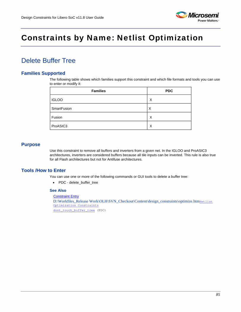
Design Constraints for Libero SoC v11.8 User Guide
85
Constraints by Name: Netlist Optimization
Delete Buffer Tree
Families Supported The following table shows which families support this constraint and which file formats and tools you can use to enter or modify it:
Families PDC
IGLOO X
SmartFusion X
Fusion X
ProASIC3 X
Purpose Use this constraint to remove all buffers and inverters from a given net. In the IGLOO and ProASIC3 architectures, inverters are considered buffers because all tile inputs can be inverted. This rule is also true for all Flash architectures but not for Antifuse architectures.
Tools /How to Enter You can use one or more of the following commands or GUI tools to delete a buffer tree: • PDC - delete_buffer_tree
See Also Constraint Entry D:\Workfiles_Release Work\OLH\SVN_Checkout\Content\design_constraints\optimize.htmNetlist Optimization Constraints
dont_touch_buffer_tree (PDC)
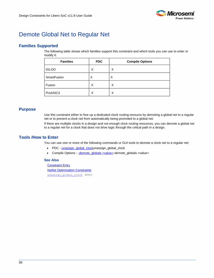
Design Constraints for Libero SoC v11.8 User Guide
86
Demote Global Net to Regular Net
Families Supported The following table shows which families support this constraint and which tools you can use to enter or modify it:
Families PDC Compile Options
IGLOO X X
SmartFusion X X
Fusion X X
ProASIC3 X X
Purpose Use this constraint either to free up a dedicated clock routing resource by demoting a global net to a regular net or to prevent a clock net from automatically being promoted to a global net. If there are multiple clocks in a design and not enough clock routing resources, you can demote a global net to a regular net for a clock that does not drive logic through the critical path in a design.
Tools /How to Enter You can use one or more of the following commands or GUI tools to demote a clock net to a regular net:
• PDC - unassign_global_clockunassign_global_clock • Compile Options - -demote_globals <value>-demote_globals <value>
See Also Constraint Entry Netlist Optimization Constraints unassign_global_clock (PDC)
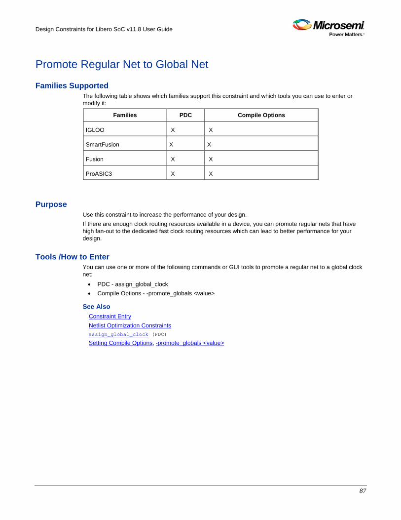
Design Constraints for Libero SoC v11.8 User Guide
87
Promote Regular Net to Global Net
Families Supported The following table shows which families support this constraint and which tools you can use to enter or modify it:
Families PDC Compile Options
IGLOO X X
SmartFusion X X
Fusion X X
ProASIC3 X X
Purpose Use this constraint to increase the performance of your design. If there are enough clock routing resources available in a device, you can promote regular nets that have high fan-out to the dedicated fast clock routing resources which can lead to better performance for your design.
Tools /How to Enter You can use one or more of the following commands or GUI tools to promote a regular net to a global clock net:
• PDC - assign_global_clock • Compile Options - -promote_globals <value>
See Also Constraint Entry Netlist Optimization Constraints assign_global_clock (PDC)
Setting Compile Options, -promote_globals <value>
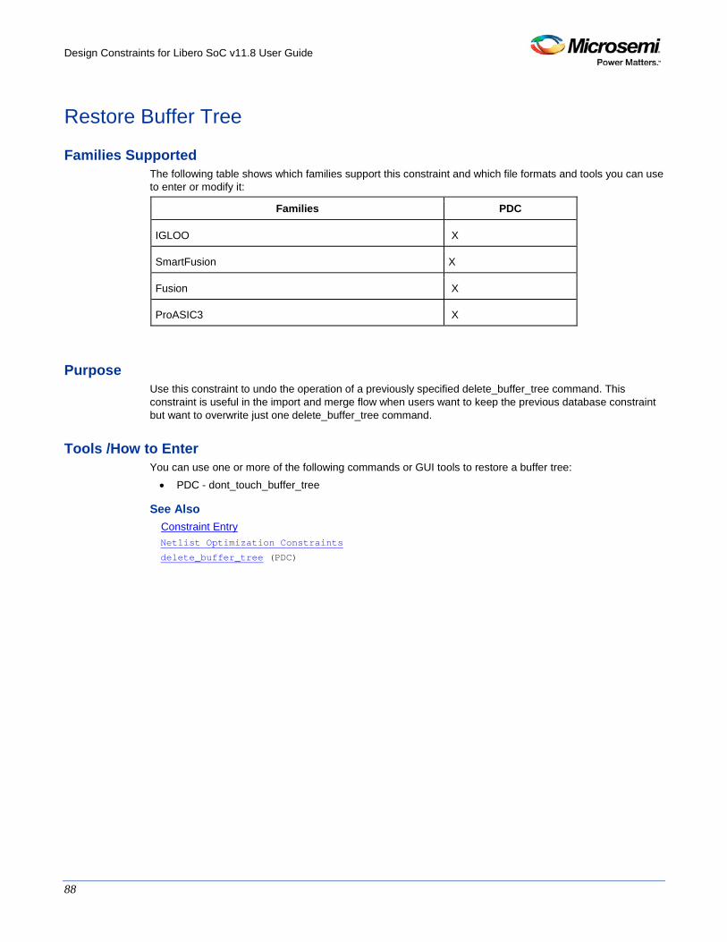
Design Constraints for Libero SoC v11.8 User Guide
88
Restore Buffer Tree
Families Supported The following table shows which families support this constraint and which file formats and tools you can use to enter or modify it:
Families PDC
IGLOO X
SmartFusion X
Fusion X
ProASIC3 X
Purpose Use this constraint to undo the operation of a previously specified delete_buffer_tree command. This constraint is useful in the import and merge flow when users want to keep the previous database constraint but want to overwrite just one delete_buffer_tree command.
Tools /How to Enter You can use one or more of the following commands or GUI tools to restore a buffer tree: • PDC - dont_touch_buffer_tree
See Also Constraint Entry Netlist Optimization Constraints
delete_buffer_tree (PDC)
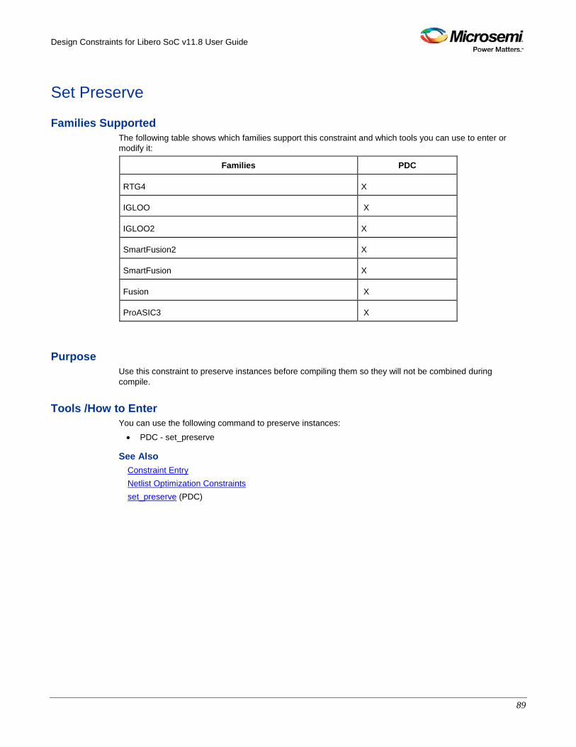
Design Constraints for Libero SoC v11.8 User Guide
89
Set Preserve
Families Supported The following table shows which families support this constraint and which tools you can use to enter or modify it:
Families PDC
RTG4 X
IGLOO X
IGLOO2 X
SmartFusion2 X
SmartFusion X
Fusion X
ProASIC3 X
Purpose Use this constraint to preserve instances before compiling them so they will not be combined during compile.
Tools /How to Enter You can use the following command to preserve instances:
• PDC - set_preserve
See Also Constraint Entry Netlist Optimization Constraints set_preserve (PDC)
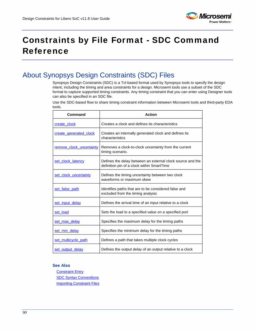
Design Constraints for Libero SoC v11.8 User Guide
90
Constraints by File Format - SDC Command Reference
About Synopsys Design Constraints (SDC) Files Synopsys Design Constraints (SDC) is a Tcl-based format used by Synopsys tools to specify the design intent, including the timing and area constraints for a design. Microsemi tools use a subset of the SDC format to capture supported timing constraints. Any timing constraint that you can enter using Designer tools can also be specified in an SDC file. Use the SDC-based flow to share timing constraint information between Microsemi tools and third-party EDA tools.
Command Action
create_clock Creates a clock and defines its characteristics
create_generated_clock Creates an internally generated clock and defines its characteristics
remove_clock_uncertainty Removes a clock-to-clock uncertainty from the current timing scenario.
set_clock_latency Defines the delay between an external clock source and the definition pin of a clock within SmartTime
set_clock_uncertainty Defines the timing uncertainty between two clock waveforms or maximum skew
set_false_path Identifies paths that are to be considered false and excluded from the timing analysis
set_input_delay Defines the arrival time of an input relative to a clock
set_load Sets the load to a specified value on a specified port
set_max_delay Specifies the maximum delay for the timing paths
set_min_delay Specifies the minimum delay for the timing paths
set_multicycle_path Defines a path that takes multiple clock cycles
set_output_delay Defines the output delay of an output relative to a clock
See Also Constraint Entry SDC Syntax Conventions Importing Constraint Files
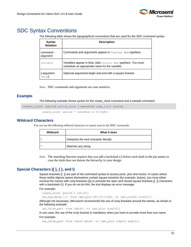
Design Constraints for Libero SoC v11.8 User Guide
91
SDC Syntax Conventions The following table shows the typographical conventions that are used for the SDC command syntax.
Syntax Notation
Description
command -argument
Commands and arguments appear in Courier New typeface.
variable Variables appear in blue, italic Courier New typeface. You must substitute an appropriate value for the variable.
[-argument value]
Optional arguments begin and end with a square bracket.
Note: SDC commands and arguments are case sensitive.
Example The following example shows syntax for the create_clock command and a sample command:
create_clock -period period_value [-waveform edge_list] source
create_clock –period 7 –waveform {2 4}{CLK1}
Wildcard Characters You can use the following wildcard characters in names used in the SDC commands:
Wildcard What it does
\ Interprets the next character literally
* Matches any string
Note: The matching function requires that you add a backslash (\) before each slash in the pin names in
case the slash does not denote the hierarchy in your design.
Special Characters ([ ], { }, and \) Square brackets ([ ]) are part of the command syntax to access ports, pins and clocks. In cases where these netlist objects names themselves contain square brackets (for example, buses), you must either enclose the names with curly brackets ({}) or precede the open and closed square brackets ([ ]) characters with a backslash (\). If you do not do this, the tool displays an error message. For example: create_clock -period 3 clk\[0\]
set_max_delay 1.5 -from [get_pins ff1\[5\]:CLK] -to [get_clocks {clk[0]}]
Although not necessary, Microsemi recommends the use of curly brackets around the names, as shown in the following example: set_false_path –from {data1} –to [get_pins {reg1:D}]
In any case, the use of the curly bracket is mandatory when you have to provide more than one name. For example: set_false_path –from {data3 data4} –to [get_pins {reg2:D reg5:D}]

Design Constraints for Libero SoC v11.8 User Guide
92
Entering Arguments on Separate Lines If a command needs to be split on multiple lines, each line except the last must end with a backslash (\) character as shown in the following example: set_multicycle_path 2 –from \
[get_pins {reg1*}] \
-to {reg2:D}
See Also About SDC Files
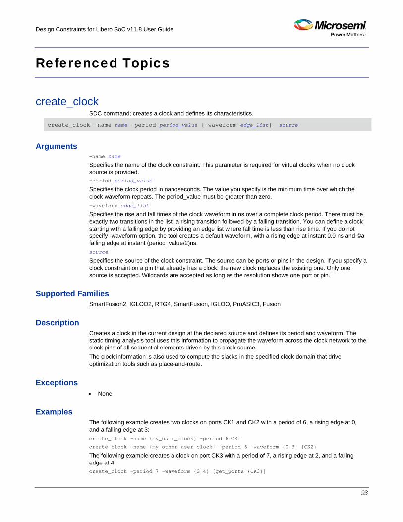
Design Constraints for Libero SoC v11.8 User Guide
93
Referenced Topics
create_clock SDC command; creates a clock and defines its characteristics.
create_clock -name name -period period_value [-waveform edge_list] source
Arguments -name name
Specifies the name of the clock constraint. This parameter is required for virtual clocks when no clock source is provided. -period period_value
Specifies the clock period in nanoseconds. The value you specify is the minimum time over which the clock waveform repeats. The period_value must be greater than zero. -waveform edge_list
Specifies the rise and fall times of the clock waveform in ns over a complete clock period. There must be exactly two transitions in the list, a rising transition followed by a falling transition. You can define a clock starting with a falling edge by providing an edge list where fall time is less than rise time. If you do not specify -waveform option, the tool creates a default waveform, with a rising edge at instant 0.0 ns and ©a falling edge at instant (period_value/2)ns. source
Specifies the source of the clock constraint. The source can be ports or pins in the design. If you specify a clock constraint on a pin that already has a clock, the new clock replaces the existing one. Only one source is accepted. Wildcards are accepted as long as the resolution shows one port or pin.
Supported Families SmartFusion2, IGLOO2, RTG4, SmartFusion, IGLOO, ProASIC3, Fusion
Description Creates a clock in the current design at the declared source and defines its period and waveform. The static timing analysis tool uses this information to propagate the waveform across the clock network to the clock pins of all sequential elements driven by this clock source. The clock information is also used to compute the slacks in the specified clock domain that drive optimization tools such as place-and-route.
Exceptions • None
Examples The following example creates two clocks on ports CK1 and CK2 with a period of 6, a rising edge at 0, and a falling edge at 3: create_clock -name {my_user_clock} -period 6 CK1
create_clock -name {my_other_user_clock} –period 6 –waveform {0 3} {CK2}
The following example creates a clock on port CK3 with a period of 7, a rising edge at 2, and a falling edge at 4: create_clock –period 7 –waveform {2 4} [get_ports {CK3}]
Design Constraints for Libero SoC v11.8 User Guide
94
Microsemi Implementation Specifics • The -waveform in SDC accepts waveforms with multiple edges within a period. In Microsemi design
implementation, only two waveforms are accepted. • SDC accepts defining a clock on many sources using a single command. In Microsemi design
implementation, only one source is accepted. • The source argument in SDC create_clock command is optional. This is in conjunction with the -name
argument in SDC to support the concept of virtual clocks. In Microsemi implementation, source is a mandatory argument as -name and virtual clocks concept is not supported.
• The -domain argument in the SDC create_clock command is not supported.
See Also Constraint Support by Family Constraint Entry Table SDC Syntax Conventions Clock Definition Create Clock Create a New Clock Constraint
create_generated_clock SDC command; creates an internally generated clock and defines its characteristics.
create_generated_clock -name {name -source reference_pin [-divide_by divide_factor] [-multiply_by multiply_factor] [-invert] source -pll_output pll_feedback_clock -pll_feedback pll_feedback_input
Arguments -name name
Specifies the name of the clock constraint. This parameter is required for virtual clocks when no clock source is provided. -source reference_pin
Specifies the reference pin in the design from which the clock waveform is to be derived. -divide_bydivide_factor
Specifies the frequency division factor. For instance if the divide_factor is equal to 2, the generated clock period is twice the reference clock period. -multiply_by multiply_factor
Specifies the frequency multiplication factor. For instance if the multiply_factor is equal to 2, the generated clock period is half the reference clock period. -invert
Specifies that the generated clock waveform is inverted with respect to the reference clock. source
Specifies the source of the clock constraint on internal pins of the design. If you specify a clock constraint on a pin that already has a clock, the new clock replaces the existing clock. Only one source is accepted. Wildcards are accepted as long as the resolution shows one pin. -pll_output pll_feedback_clock
Specifies the output pin of the PLL which is used as the external feedback clock. This pin must drive the feedback input pin of the PLL specified using the –pll_feedback option. The PLL will align the rising edge of the reference input clock to the feedback clock. This is a mandatory argument if the PLL is operating in external feedback mode. -pll_feedback pll_feedback_input
Design Constraints for Libero SoC v11.8 User Guide
95
Specifies the feedback input pin of the PLL. This pin must be driven by the output pin of the PLL specified using the –pll_output option. The PLL will align the rising edge of the reference input clock to the external feedback clock. This is a mandatory argument if the PLL is operating in external feedback mode.
Supported Families SmartFusion2, IGLOO2, RTG4, SmartFusion, IGLOO, ProASIC3, Fusion
Description Creates a generated clock in the current design at a declared source by defining its frequency with respect to the frequency at the reference pin. The static timing analysis tool uses this information to compute and propagate its waveform across the clock network to the clock pins of all sequential elements driven by this source. The generated clock information is also used to compute the slacks in the specified clock domain that drive optimization tools such as place-and-route.
Examples The following example creates a generated clock on pin U1/reg1:Q with a period twice as long as the period at the reference port CLK. create_generated_clock -name {my_user_clock} –divide_by 2 –source [get_ports {CLK}] U1/reg1/Q
The following example creates a generated clock at the primary output of myPLL with a period ¾ of the period at the reference pin clk. create_generated_clock –divide_by 3 –multiply_by 4 -source clk [get_pins {myPLL/CLK1}]
The following example creates a generated clock named system_clk on the GL2 output pin of FCCC_0 with a period equal to half the period of the source clock. The constraint also identifies GL2 output pin as the external feedback clock source and CLK2 as the feedback input pin for FCCC_0. create_generated_clock -name { system_clk } \
-multiply_by 2 \
-source { FCCC_0/CCC_INST/CLK3_PAD } \
-pll_output { FCCC_0/CCC_INST/GL2 } \
-pll_feedback { FCCC_0/CCC_INST/CLK2 } \
{ FCCC_0/CCC_INST/GL2 }
Microsemi Implementation Specifics • SDC accepts either –multiply_by or –divide_by option. In Microsemi design implementation, both are
accepted to accurately model the PLL behavior. • SDC accepts defining a generated clock on many sources using a single command. In Microsemi
design implementation, only one source is accepted. • The -duty_cycle ,-edges and –edge_shift options in the SDC create_generated_clock command are
not supported in Microsemi design implementation.
See Also Constraint Support by Family Constraint Entry Table SDC Syntax Conventions Create Generated Clock Constraint (SDC)
remove_clock_uncertainty SDC command; Removes a clock-to-clock uncertainty from the current timing scenario.
Design Constraints for Libero SoC v11.8 User Guide
96
remove_clock_uncertainty -from | -rise_from | -fall_from from_clock_list -to | -rise_to| -fall_to to_clock_list -setup {value} -hold {value}
remove_clock_uncertainty -id constraint_ID
Arguments -from
Specifies that the clock-to-clock uncertainty applies to both rising and falling edges of the source clock list. You can specify only one of the -from, -rise_from, or -fall_from arguments for the constraint to be valid. -rise_from
Specifies that the clock-to-clock uncertainty applies only to rising edges of the source clock list. You can specify only one of the -from, -rise_from, or -fall_from arguments for the constraint to be valid. -fall_from
Specifies that the clock-to-clock uncertainty applies only to falling edges of the source clock list. You can specify only one of the -from, -rise_from, or -fall_from arguments for the constraint to be valid. from_clock_list
Specifies the list of clock names as the uncertainty source. -to
Specifies that the clock-to-clock uncertainty applies to both rising and falling edges of the destination clock list. You can specify only one of the -to, -rise_to , or -fall_to arguments for the constraint to be valid. -rise_to
Specifies that the clock-to-clock uncertainty applies only to rising edges of the destination clock list. You can specify only one of the -to, -rise_to , or -fall_to arguments for the constraint to be valid. -fall_to
Specifies that the clock-to-clock uncertainty applies only to falling edges of the destination clock list. You can specify only one of the -to, -rise_to , or -fall_to arguments for the constraint to be valid. to_clock_list
Specifies the list of clock names as the uncertainty destination. -setup
Specifies that the uncertainty applies only to setup checks. If none or both -setup and -hold are present, the uncertainty applies to both setup and hold checks. -hold
Specifies that the uncertainty applies only to hold checks. If none or both -setup and -hold are present, the uncertainty applies to both setup and hold checks. -id constraint_ID
Specifies the ID of the clock constraint to remove from the current scenario. You must specify either the exact parameters to set the constraint or its constraint ID.
Supported Families SmartFusion2, IGLOO2, RTG4, SmartFusion, IGLOO, ProASIC3, Fusion
Description Removes a clock-to-clock uncertainty from the specified clock in the current scenario. If the specified arguments do not match clocks with an uncertainty constraint in the current scenario, or if the specified ID does not refer to a clock-to-clock uncertainty constraint, this command fails. Do not specify both the exact arguments and the ID.
Exceptions None
Design Constraints for Libero SoC v11.8 User Guide
97
Examples remove_clock_uncertainty -from Clk1 -to Clk2
remove_clock_uncertainty -from Clk1 -fall_to { Clk2 Clk3 } -setup
remove_clock_uncertainty 4.3 -fall_from { Clk1 Clk2 } -rise_to *
remove_clock_uncertainty 0.1 -rise_from [ get_clocks { Clk1 Clk2 } ] -fall_to { Clk3 Clk4 } -setup
remove_clock_uncertainty 5 -rise_from Clk1 -to [ get_clocks {*} ]
remove_clock_uncertainty -id $clockId
See Also Constraint Support by Family Constraint Entry Table SDC Syntax Conventions set_clock_uncertainty
set_clock_latency SDC command; defines the delay between an external clock source and the definition pin of a clock within SmartTime.
set_clock_latency -source [-rise][-fall][-early][-late] delay clock
Arguments -source
Specifies a clock source latency on a clock pin. -rise
Specifies the edge for which this constraint will apply. If neither or both rise are passed, the same latency is applied to both edges. -fall
Specifies the edge for which this constraint will apply. If neither or both rise are passed, the same latency is applied to both edges. -invert
Specifies that the generated clock waveform is inverted with respect to the reference clock. -late
Optional. Specifies that the latency is late bound on the latency. The appropriate bound is used to provide the most pessimistic timing scenario. However, if the value of "-late" is less than the value of "-early", optimistic timing takes place which could result in incorrect analysis. If neither or both "-early" and "-late" are provided, the same latency is used for both bounds, which results in the latency having no effect for single clock domain setup and hold checks. -early
Optional. Specifies that the latency is early bound on the latency. The appropriate bound is used to provide the most pessimistic timing scenario. However, if the value of "-late" is less than the value of "-early", optimistic timing takes place which could result in incorrect analysis. If neither or both "-early" and "-late" are provided, the same latency is used for both bounds, which results in the latency having no effect for single clock domain setup and hold checks. delay
Specifies the latency value for the constraint. clock
Specifies the clock to which the constraint is applied. This clock must be constrained.
Design Constraints for Libero SoC v11.8 User Guide
98
Supported Families SmartFusion2, IGLOO2, RTG4, SmartFusion, IGLOO, ProASIC3, Fusion
Description Clock source latency defines the delay between an external clock source and the definition pin of a clock within SmartTime. It behaves much like an input delay constraint. You can specify both an "early" delay and a"late" delay for this latency, providing an uncertainty which SmartTime propagates through its calculations. Rising and falling edges of the same clock can have different latencies. If only one value is provided for the clock source latency, it is taken as the exact latency value, for both rising and falling edges.
Exceptions None
Examples The following example sets an early clock source latency of 0.4 on the rising edge of main_clock. It also sets a clock source latency of 1.2, for both the early and late values of the falling edge of main_clock. The late value for the clock source latency for the falling edge of main_clock remains undefined. set_clock_latency –source –rise –early 0.4 { main_clock }
set_clock_latency –source –fall 1.2 { main_clock }
Microsemi Implementation Specifics SDC accepts a list of clocks to -set_clock_latency. In Microsemi design implementation, only one clock pin can have its source latency specified per command.
See Also Constraint Support by Family Constraint Entry Table SDC Syntax Conventions
set_clock_to_output SDC command; defines the timing budget available inside the FPGA for an output relative to a clock.
set_clock_to_output delay_value -clock clock_ref [–max] [–min] [–clock_fall] output_list
Arguments delay_value
Specifies the clock to output delay in nanoseconds. This time represents the amount of time available inside the FPGA between the active clock edge and the data change at the output port. -clock clock_ref
Specifies the reference clock to which the specified clock to output is related. This is a mandatory argument. -max
Specifies that delay_value refers to the maximum clock to output at the specified output. If you do not specify –max or –min options, the tool assumes maximum and minimum clock to output delays to be equal. -min
Design Constraints for Libero SoC v11.8 User Guide
99
Specifies that delay_value refers to the minimum clock to output at the specified output. If you do not specify –max or –min options, the tool assumes maximum and minimum clock to output delays to be equal. -clock_fall
Specifies that the delay is relative to the falling edge of the reference clock. The default is the rising edge. output_list
Provides a list of output ports in the current design to which delay_value is assigned. If you need to specify more than one object, enclose the objects in braces ({}).
Supported Families SmartFusion2, IGLOO2, RTG4, SmartFusion, IGLOO, ProASIC3, Fusion
Description The set_clock_to_output command specifies the clock to output maximum and minimum delays on output ports relative to a clock edge. This usually represents a combinational path delay from a register internal to the current design to the output port. For in/out (bidirectional) ports, you can specify the path delays for both input and output modes. The tool uses clock to output delays for paths ending at primary outputs. A clock is a singleton that represents the name of a defined clock constraint. This can be an object accessor that will refer to one clock. For example: [get_clocks {system_clk}]
[get_clocks {sys*_clk}]
Examples The following example sets a maximum clock to output delay of 12 ns and a minimum clock to output delay of 6 ns for port data_out relative to the rising edge of CLK1: set_clock_to_output 12 -clock [get_clocks CLK1] -max [get_ports data_out]
set_clock_to_output 6 -clock [get_clocks CLK1] -min [get_ports data_out]
See Also Constraint Support by Family Constraint Entry Table SDC Syntax Conventions
set_clock_uncertainty SDC command; defines the timing uncertainty between two clock waveforms or maximum skew.
set_clock_uncertainty uncertainty (-from | -rise_from | -fall_from) from_clock_list (-to | -rise_to | -fall_to) to_clock_list [-setup | -hold]
Arguments uncertainty
Specifies the time in nanoseconds that represents the amount of variation between two clock edges. The value must be a positive floating point number. -from
Specifies that the clock-to-clock uncertainty applies to both rising and falling edges of the source clock list. You can specify only one of the -from, -rise_from, or -fall_from arguments for the constraint to be valid. This option is the default. -rise_from
Specifies that the clock-to-clock uncertainty applies only to rising edges of the source clock list. You can specify only one of the -from, -rise_from, or -fall_from arguments for the constraint to be valid.
Design Constraints for Libero SoC v11.8 User Guide
100
-fall_from
Specifies that the clock-to-clock uncertainty applies only to falling edges of the source clock list. You can specify only one of the -from, -rise_from, or -fall_from arguments for the constraint to be valid. from_clock_list
Specifies the list of clock names as the uncertainty source. -to
Specifies that the clock-to-clock uncertainty applies to both rising and falling edges of the destination clock list. You can specify only one of the -to, -rise_to , or -fall_to arguments for the constraint to be valid. -rise_to
Specifies that the clock-to-clock uncertainty applies only to rising edges of the destination clock list. You can specify only one of the -to, -rise_to , or -fall_to arguments for the constraint to be valid. -fall_to
Specifies that the clock-to-clock uncertainty applies only to falling edges of the destination clock list. You can specify only one of the -to, -rise_to , or -fall_to arguments for the constraint to be valid. to_clock_list
Specifies the list of clock names as the uncertainty destination. -setup
Specifies that the uncertainty applies only to setup checks. If you do not specify either option (-setup or -hold ) or if you specify both options, the uncertainty applies to both setup and hold checks. -hold
Specifies that the uncertainty applies only to hold checks. If you do not specify either option (-setup or -hold ) or if you specify both options, the uncertainty applies to both setup and hold checks.
Supported Families SmartFusion2, IGLOO2, RTG4, SmartFusion, IGLOO, ProASIC3, Fusion
Description Clock uncertainty defines the timing between an two clock waveforms or maximum clock skew. Both setup and hold checks must account for clock skew. However, for setup check, SmartTime looks for the smallest skew. This skew is computed by using the maximum insertion delay to the launching sequential component and the shortest insertion delay to the receiving component. For hold check, SmartTime looks for the largest skew. This skew is computed by using the shortest insertion delay to the launching sequential component and the largest insertion delay to the receiving component. SmartTime makes this distinction automatically.
Exceptions None
Examples The following example defines two clocks and sets the uncertainty constraints, which analyzes the inter-clock domain between clk1 and clk2. create_clock –period 10 clk1
create_generated_clock –name clk2 -source clk1 -multiply_by 2 sclk1
set_clock_uncertainty 0.4 -rise_from clk1 -rise_to clk2
Microsemi Implementation Specifics • SDC accepts a list of clocks to -set_clock_uncertainty.
Design Constraints for Libero SoC v11.8 User Guide
101
See Also Constraint Support by Family Constraint Entry Table SDC Syntax Conventions create_clock (SDC) create_generated_clock (SDC) remove_clock_uncertainty
set_disable_timing SDC command; disables timing arcs within the specified cell and returns the ID of the created constraint if the command succeeded.
set_disable_timing [-from from_port] [-to to_port] cell_name
Arguments -from from_port
Specifies the starting port.
-to to_port
Specifies the ending port.
cell_name
Specifies the name of the cell in which timing arcs will be disabled.
Supported Families SmartFusion2, IGLOO2, RTG4, SmartFusion, IGLOO, ProASIC3, Fusion
Description This command disables the timing arcs in the specified cell, and returns the ID of the created constraint if the command succeeded. The –from and –to arguments must either both be present or both omitted for the constraint to be valid.
Examples The following example disables the arc between a2:A and a2:Y.
set_disable_timing -from port1 -to port2 cellname
This command ensures that the arc is disabled within a cell instead of between cells.
Microsemi Implementation Specifics • None
See Also Constraint Support by Family
Constraint Entry Table
SDC Syntax Conventions
Design Constraints for Libero SoC v11.8 User Guide
102
set_external_check SDC command; defines the external setup and hold delays for an input relative to a clock.
set_external_check delay_value -clock clock_ref [–setup] [–hold] [–clock_fall] input_list
Arguments delay_value
Specifies the external setup or external hold delay in nanoseconds. This time represents the amount of time available inside the FPGA for the specified input after a clock edge. -clock clock_ref
Specifies the reference clock to which the specified external check is related. This is a mandatory argument. -setup
Specifies that delay_value refers to the setup check at the specified input. This is a mandatory argument if –hold is not used. You must specify either -setup or -hold option. -clock_fall
Specifies that the delay is relative to the falling edge of the reference clock. The default is the rising edge. input_list
Provides a list of input ports in the current design to which delay_value is assigned. If you need to specify more than one object, enclose the objects in braces ({}).
Supported Families SmartFusion2, IGLOO2, RTG4, SmartFusion, IGLOO, ProASIC3, Fusion
Description The set_external_check command specifies the external setup and hold times on input ports relative to a clock edge. This usually represents a combinational path delay from the input port to the clock pin of a register internal to the current design. For in/out (bidirectional) ports, you can specify the path delays for both input and output modes. The tool uses external setup and external hold times for paths starting at primary inputs. A clock is a singleton that represents the name of a defined clock constraint. This can be an object accessor that will refer to one clock. For example: [get_clocks {system_clk}]
[get_clocks {sys*_clk}]
Examples The following example sets an external setup check of 12 ns and an external hold check of 6 ns for port data_in relative to the rising edge of CLK1: set_external_check 12 -clock [get_clocks CLK1] -setup [get_ports data_in]
set_external_check 6 -clock [get_clocks CLK1] -hold [get_ports data_in]
See Also Constraint Support by Family Constraint Entry Table SDC Syntax Conventions
Design Constraints for Libero SoC v11.8 User Guide
103
set_false_path SDC command; identifies paths that are considered false and excluded from the timing analysis.
set_false_path [-from from_list] [-through through_list] [-to to_list]
Arguments -from from_list
Specifies a list of timing path starting points. A valid timing starting point is a clock, a primary input, an inout port, or a clock pin of a sequential cell. -through through_list
Specifies a list of pins, ports, cells, or nets through which the disabled paths must pass. -to to_list
Specifies a list of timing path ending points. A valid timing ending point is a clock, a primary output, an inout port, or a data pin of a sequential cell.
Supported Families SmartFusion2, IGLOO2, RTG4, SmartFusion, IGLOO, ProASIC3, Fusion
Description The set_false_path command identifies specific timing paths as being false. The false timing paths are paths that do not propagate logic level changes. This constraint removes timing requirements on these false paths so that they are not considered during the timing analysis. The path starting points are the input ports or register clock pins, and the path ending points are the register data pins or output ports. This constraint disables setup and hold checking for the specified paths. The false path information always takes precedence over multiple cycle path information and overrides maximum delay constraints. If more than one object is specified within one -through option, the path can pass through any objects.
Examples The following example specifies all paths from clock pins of the registers in clock domain clk1 to data pins of a specific register in clock domain clk2 as false paths: set_false_path –from [get_clocks {clk1}] –to reg_2:D
The following example specifies all paths through the pin U0/U1:Y to be false: set_false_path -through U0/U1:Y
Microsemi Implementation Specifics SDC accepts multiple -through options in a single constraint to specify paths that traverse multiple points in the design. In Microsemi design implementation, only one –through option is accepted.
See Also Constraint Support by Family Constraint Entry Table SDC Syntax Conventions Set False Path Constraint
Design Constraints for Libero SoC v11.8 User Guide
104
set_input_delay SDC command; defines the arrival time of an input relative to a clock.
set_input_delay delay_value -clock clock_ref [–max] [–min] [–clock_fall] input_list
Arguments delay_value
Specifies the arrival time in nanoseconds that represents the amount of time for which the signal is available at the specified input after a clock edge. -clock clock_ref
Specifies the clock reference to which the specified input delay is related. This is a mandatory argument. If you do not specify -max or -min options, the tool assumes the maximum and minimum input delays to be equal. -max
Specifies that delay_value refers to the longest path arriving at the specified input. If you do not specify -max or -min options, the tool assumes maximum and minimum input delays to be equal. -min
Specifies that delay_value refers to the shortest path arriving at the specified input. If you do not specify -max or -min options, the tool assumes maximum and minimum input delays to be equal. -clock_fall
Specifies that the delay is relative to the falling edge of the clock reference. The default is the rising edge. input_list
Provides a list of input ports in the current design to which delay_value is assigned. If you need to specify more than one object, enclose the objects in braces ({}).
Supported Families SmartFusion2, IGLOO2, RTG4, SmartFusion, IGLOO, ProASIC3, Fusion and IGLOOe, except ProASIC3 nano and ProASIC3L
Description The set_input_delay command sets input path delays on input ports relative to a clock edge. This usually represents a combinational path delay from the clock pin of a register external to the current design. For in/out (bidirectional) ports, you can specify the path delays for both input and output modes. The tool adds input delay to path delay for paths starting at primary inputs. A clock is a singleton that represents the name of a defined clock constraint. This can be:
• a single port name used as source for a clock constraint • a single pin name used as source for a clock constraint; for instance reg1:CLK. This name can be
hierarchical (for instance toplevel/block1/reg2:CLK) • an object accessor that will refer to one clock: [get_clocks {clk}]
Examples The following example sets an input delay of 1.2ns for port data1 relative to the rising edge of CLK1: set_input_delay 1.2 -clock [get_clocks CLK1] [get_ports data1]
The following example sets a different maximum and minimum input delay for port IN1 relative to the falling edge of CLK2: set_input_delay 1.0 -clock_fall -clock CLK2 –min {IN1}
set_input_delay 1.4 -clock_fall -clock CLK2 –max {IN1}
Design Constraints for Libero SoC v11.8 User Guide
105
Microsemi Implementation Specifics In SDC, the -clock is an optional argument that allows you to set input delay for combinational designs. Microsemi Implementation currently requires this argument.
See Also Constraint Support by Family Constraint Entry Table SDC Syntax Conventions Set Input Delay
set_load SDC command; sets the load to a specified value on a specified port.
set_load capacitance port_list
Arguments capacitance
Specifies the capacitance value that must be set on the specified ports. port_list
Specifies a list of ports in the current design on which the capacitance is to be set.
Supported Families SmartFusion2, IGLOO2, RTG4, SmartFusion, IGLOO, ProASIC3, Fusion
Description The load constraint enables the Designer software to account for external capacitance at a specified port. You cannot set load constraint on the nets. When you specify this constraint on the output ports, it impacts the delay calculation on the specified ports.
Examples The following examples show how to set output capacitance on different output ports: set_load 35 out_p
set_load 40 {O1 02}
set_load 25 [get_ports out]
Microsemi Implementation Specifics • In SDC, you can use the set_load command to specify capacitance value on nets. Microsemi
Implementation only supports output ports.
See Also Constraint Support by Family Constraint Entry Table SDC Syntax Conventions Set Load on Port
Design Constraints for Libero SoC v11.8 User Guide
106
set_max_delay (SDC) SDC command; specifies the maximum delay for the timing paths.
set_max_delay delay_value [-from from_list] [-to to_list]
Arguments delay_value
Specifies a floating point number in nanoseconds that represents the required maximum delay value for specified paths.
• If the path starting point is on a sequential device, the tool includes clock skew in the computed delay.
• If the path starting point has an input delay specified, the tool adds that delay value to the path delay.
• If the path ending point is on a sequential device, the tool includes clock skew and library setup time in the computed delay.
• If the ending point has an output delay specified, the tool adds that delay to the path delay.
-from from_list
Specifies a list of timing path starting points. A valid timing starting point is a clock, a primary input, an inout port, or a clock pin of a sequential cell. -to to_list
Specifies a list of timing path ending points. A valid timing ending point is a clock, a primary output, an inout port, or a data pin of a sequential cell.
Supported Families SmartFusion2, IGLOO2, RTG4, SmartFusion, IGLOO, ProASIC3, Fusion
Description This command specifies the required maximum delay for timing paths in the current design. The path length for any startpoint in from_list to any endpoint in to_list must be less than delay_value. The tool automatically derives the individual maximum delay targets from clock waveforms and port input or output delays. For more information, refer to the create_clock, set_input_delay, and set_output_delay commands. The maximum delay constraint is a timing exception. This constraint overrides the default single cycle timing relationship for one or more timing paths. This constraint also overrides a multicycle path constraint.
Examples The following example sets a maximum delay by constraining all paths from ff1a:CLK or ff1b:CLK to ff2e:D with a delay less than 5 ns: set_max_delay 5 -from {ff1a:CLK ff1b:CLK} -to {ff2e:D}
The following example sets a maximum delay by constraining all paths to output ports whose names start by “out” with a delay less than 3.8 ns: set_max_delay 3.8 -to [get_ports out*]
Design Constraints for Libero SoC v11.8 User Guide
107
Microsemi Implementation Specifics The –through option in the set_max_delay SDC command is not supported.
See Also Constraint Support by Family Constraint Entry Table SDC Syntax Conventions Set Max Delay
set_min_delay SDC command; specifies the minimum delay for the timing paths.
set_min_delay delay_value [-from from_list] [-to to_list]
Arguments delay_value
Specifies a floating point number in nanoseconds that represents the required minimum delay value for specified paths.
• If the path starting point is on a sequential device, the tool includes clock skew in the computed delay.
• If the path starting point has an input delay specified, the tool adds that delay value to the path delay.
• If the path ending point is on a sequential device, the tool includes clock skew and library setup time in the computed delay.
• If the ending point has an output delay specified, the tool adds that delay to the path delay.
-from from_list
Specifies a list of timing path starting points. A valid timing starting point is a clock, a primary input, an inout port, or a clock pin of a sequential cell.
-to to_list
Specifies a list of timing path ending points. A valid timing ending point is a clock, a primary output, an inout port, or a data pin of a sequential cell.
Supported Families SmartFusion2, IGLOO2, RTG4, SmartFusion, IGLOO, ProASIC3, Fusion
Description This command specifies the required minimum delay for timing paths in the current design. The path length for any startpoint in from_list to any endpoint in to_list must be less than delay_value. The tool automatically derives the individual minimum delay targets from clock waveforms and port input or output delays. For more information, refer to the create_clock, set_input_delay, and set_output_delay commands.
Design Constraints for Libero SoC v11.8 User Guide
108
The minimum delay constraint is a timing exception. This constraint overrides the default single cycle timing relationship for one or more timing paths. This constraint also overrides a multicycle path constraint.
Examples The following example sets a minimum delay by constraining all paths from ff1a:CLK or ff1b:CLK to ff2e:D with a delay less than 5 ns:
set_min_delay 5 -from {ff1a:CLK ff1b:CLK} -to {ff2e:D}
The following example sets a minimum delay by constraining all paths to output ports whose names start by “out” with a delay less than 3.8 ns:
set_min_delay 3.8 -to [get_ports out*]
Microsemi Implementation Specifics The –through option in the set_min_delay SDC command is not supported.
See Also Constraint Support by Family
Constraint Entry Table
SDC Syntax Conventions
set_multicycle_path SDC command; defines a path that takes multiple clock cycles.
set_multicycle_path ncycles [-setup] [-hold] [-from from_list] [–through through_list] [-to to_list]
Arguments ncycles
Specifies an integer value that represents a number of cycles the data path must have for setup or hold check. The value is relative to the starting point or ending point clock, before data is required at the ending point. -setup
Optional. Applies the cycle value for the setup check only. This option does not affect the hold check. The default hold check will be applied unless you have specified another set_multicycle_path command for the hold value. -hold
Optional. Applies the cycle value for the hold check only. This option does not affect the setup check. Note: If you do not specify "-setup" or "-hold", the cycle value is applied to the setup check and the
default hold check is performed (ncycles -1). -from from_list
Specifies a list of timing path starting points. A valid timing starting point is a clock, a primary input, an inout port, or a clock pin of a sequential cell. -through through_list
Specifies a list of pins or ports through which the multiple cycle paths must pass. -to to_list
Specifies a list of timing path ending points. A valid timing ending point is a clock, a primary output, an inout port, or a data pin of a sequential cell.
Design Constraints for Libero SoC v11.8 User Guide
109
Supported Families SmartFusion2, IGLOO2, RTG4, SmartFusion, IGLOO, ProASIC3, Fusion
Description Setting multiple cycle paths constraint overrides the single cycle timing relationships between sequential elements by specifying the number of cycles that the data path must have for setup or hold checks. If you change the multiplier, it affects both the setup and hold checks. False path information always takes precedence over multiple cycle path information. A specific maximum delay constraint overrides a general multiple cycle path constraint. If you specify more than one object within one -through option, the path passes through any of the objects.
Examples The following example sets all paths between reg1 and reg2 to 3 cycles for setup check. Hold check is measured at the previous edge of the clock at reg2. set_multicycle_path 3 -from [get_pins {reg1}] –to [get_pins {reg2}]
The following example specifies that four cycles are needed for setup check on all paths starting at the registers in the clock domain ck1. Hold check is further specified with two cycles instead of the three cycles that would have been applied otherwise. set_multicycle_path 4 -setup -from [get_clocks {ck1}]
set_multicycle_path 2 -hold -from [get_clocks {ck1}]
Microsemi Implementation Specifics • SDC allows multiple priority management on the multiple cycle path constraint depending on the scope
of the object accessors. In Microsemi design implementation, such priority management is not supported. All multiple cycle path constraints are handled with the same priority.
See Also Constraint Support by Family Constraint Entry Table SDC Syntax Conventions Set Multicycle Path
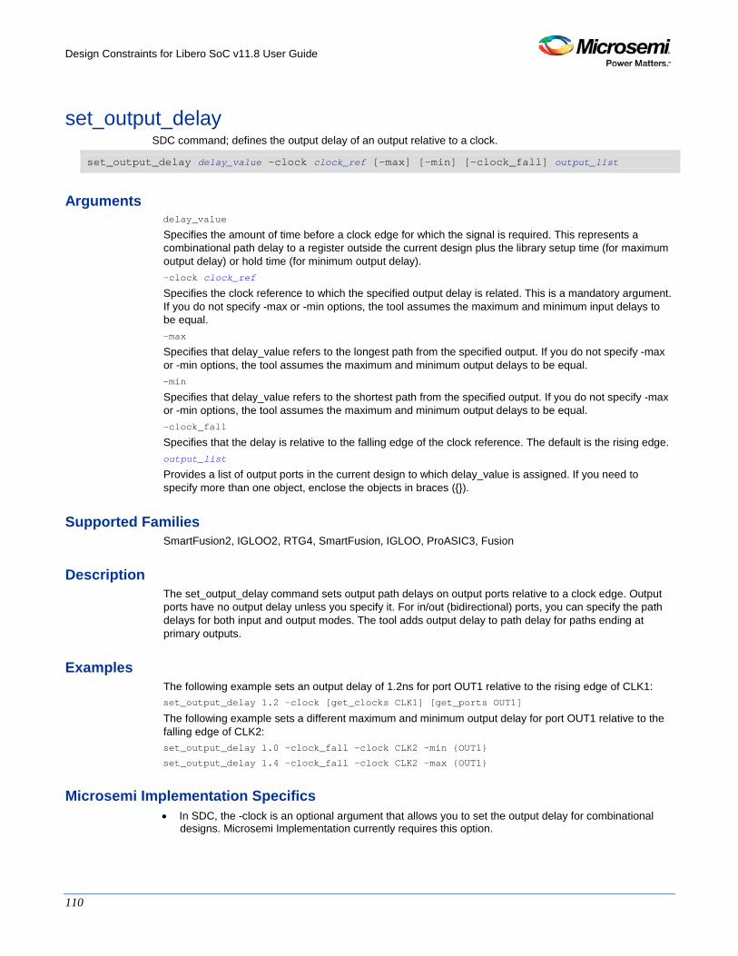
Design Constraints for Libero SoC v11.8 User Guide
110
set_output_delay SDC command; defines the output delay of an output relative to a clock.
set_output_delay delay_value -clock clock_ref [–max] [–min] [–clock_fall] output_list
Arguments delay_value
Specifies the amount of time before a clock edge for which the signal is required. This represents a combinational path delay to a register outside the current design plus the library setup time (for maximum output delay) or hold time (for minimum output delay). -clock clock_ref
Specifies the clock reference to which the specified output delay is related. This is a mandatory argument. If you do not specify -max or -min options, the tool assumes the maximum and minimum input delays to be equal. -max
Specifies that delay_value refers to the longest path from the specified output. If you do not specify -max or -min options, the tool assumes the maximum and minimum output delays to be equal. -min
Specifies that delay_value refers to the shortest path from the specified output. If you do not specify -max or -min options, the tool assumes the maximum and minimum output delays to be equal. -clock_fall
Specifies that the delay is relative to the falling edge of the clock reference. The default is the rising edge. output_list
Provides a list of output ports in the current design to which delay_value is assigned. If you need to specify more than one object, enclose the objects in braces ({}).
Supported Families SmartFusion2, IGLOO2, RTG4, SmartFusion, IGLOO, ProASIC3, Fusion
Description The set_output_delay command sets output path delays on output ports relative to a clock edge. Output ports have no output delay unless you specify it. For in/out (bidirectional) ports, you can specify the path delays for both input and output modes. The tool adds output delay to path delay for paths ending at primary outputs.
Examples The following example sets an output delay of 1.2ns for port OUT1 relative to the rising edge of CLK1: set_output_delay 1.2 -clock [get_clocks CLK1] [get_ports OUT1]
The following example sets a different maximum and minimum output delay for port OUT1 relative to the falling edge of CLK2: set_output_delay 1.0 -clock_fall -clock CLK2 –min {OUT1}
set_output_delay 1.4 -clock_fall -clock CLK2 –max {OUT1}
Microsemi Implementation Specifics • In SDC, the -clock is an optional argument that allows you to set the output delay for combinational
designs. Microsemi Implementation currently requires this option.
Design Constraints for Libero SoC v11.8 User Guide
111
See Also Constraint Support by Family Constraint Entry Table SDC Syntax Conventions Set Output Delay
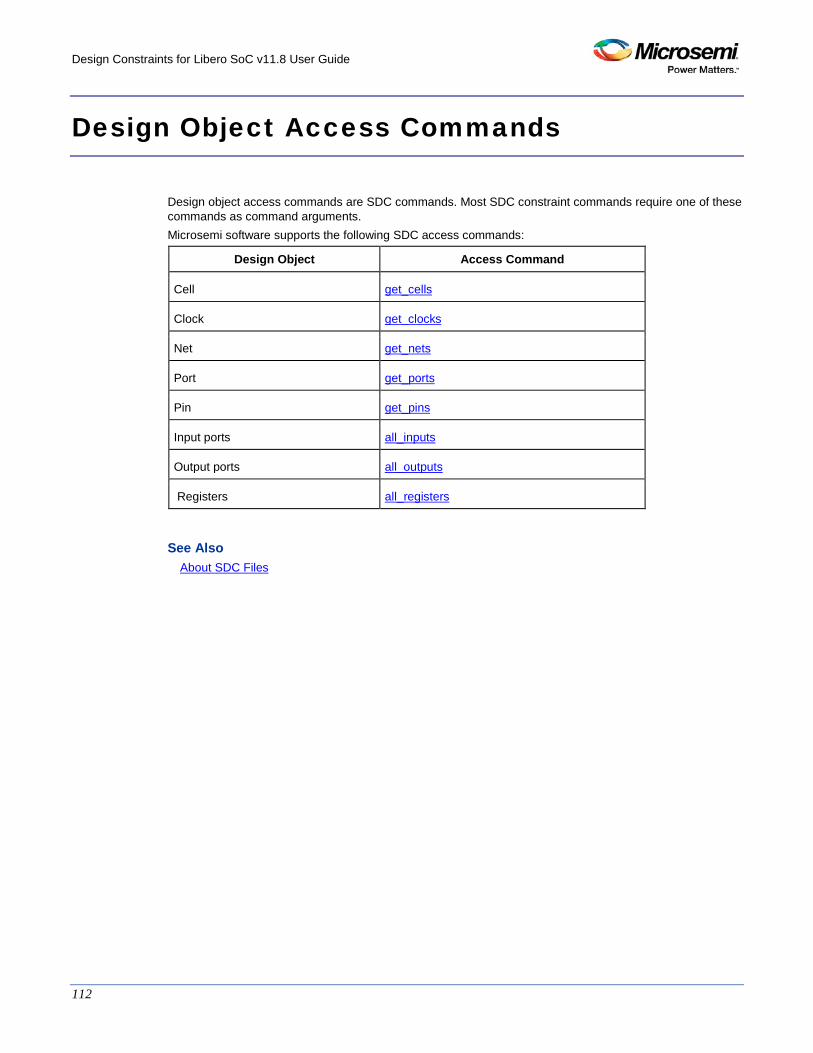
Design Constraints for Libero SoC v11.8 User Guide
112
Design Object Access Commands
Design object access commands are SDC commands. Most SDC constraint commands require one of these commands as command arguments. Microsemi software supports the following SDC access commands:
Design Object Access Command
Cell get_cells
Clock get_clocks
Net get_nets
Port get_ports
Pin get_pins
Input ports all_inputs
Output ports all_outputs
Registers all_registers
See Also About SDC Files

Design Constraints for Libero SoC v11.8 User Guide
113
all_inputs Design object access command; returns all the input or inout ports of the design.
all_inputs
Arguments • None
Supported Families SmartFusion2, IGLOO2, RTG4, SmartFusion, IGLOO, ProASIC3, Fusion
Exceptions • None
Example set_max_delay -from [all_inputs] -to [get_clocks ck1]
Microsemi Implementation Specifics • None
See Also Constraint Support by Family Constraint Entry Table SDC Syntax Conventions
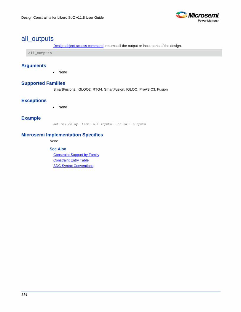
Design Constraints for Libero SoC v11.8 User Guide
114
all_outputs Design object access command; returns all the output or inout ports of the design.
all_outputs
Arguments • None
Supported Families SmartFusion2, IGLOO2, RTG4, SmartFusion, IGLOO, ProASIC3, Fusion
Exceptions • None
Example set_max_delay -from [all_inputs] -to [all_outputs]
Microsemi Implementation Specifics None
See Also Constraint Support by Family Constraint Entry Table SDC Syntax Conventions
Design Constraints for Libero SoC v11.8 User Guide
115
all_registers Design object access command; returns either a collection of register cells or register pins, whichever you specify.
all_registers [-clock clock_name] [-cells] [-data_pins ] [-clock_pins] [-async_pins] [-output_pins]
Arguments -clock clock_name
Creates a collection of register cells or register pins in the specified clock domain. -cells
Creates a collection of register cells. This is the default. This option cannot be used in combination with any other option. -data_pins
Creates a collection of register data pins. -clock_pins
Creates a collection of register clock pins. -async_pins
Creates a collection of register asynchronous pins. -output_pins
Creates a collection of register output pins.
Supported Families SmartFusion2, IGLOO2, RTG4, SmartFusion, IGLOO, ProASIC3, Fusion
Description This command creates either a collection of register cells (default) or register pins, whichever is specified. If you do not specify an option, this command creates a collection of register cells.
Exceptions • None
Examples set_max_delay 2 -from [all_registers] -to [get_ports {out}]
set_max_delay 3 –to [all_registers –async_pins]
set_false_path –from [all_registers –clock clk150]
set_multicycle_path –to [all_registers –clock c* -data_pins
–clock_pins]
Microsemi Implementation Specifics • None
See Also Constraint Support by Family Constraint Entry Table SDC Syntax Conventions
Design Constraints for Libero SoC v11.8 User Guide
116
get_cells Design object access command; returns the cells (instances) specified by the pattern argument.
get_cells pattern
Arguments pattern
Specifies the pattern to match the instances to return. For example, "get_cells U18*" returns all instances starting with the characters "U18", where “*” is a wildcard that represents any character string.
Supported Families SmartFusion2, IGLOO2, RTG4, SmartFusion, IGLOO, ProASIC3, Fusion
Description This command returns a collection of instances matching the pattern you specify. You can only use this command as part of a –from, -to, or –through argument for the following constraint exceptions: set_max delay, set_multicycle_path, and set_false_path design constraints.
Exceptions None
Examples set_max_delay 2 -from [get_cells {reg*}] -to [get_ports {out}]
set_false_path –through [get_cells {Rblock/muxA}]
Microsemi Implementation Specifics • None
See Also Constraint Support by Family Constraint Entry Table SDC Syntax Conventions
Design Constraints for Libero SoC v11.8 User Guide
117
get_clocks Design object access command; returns the specified clock.
get_clocks pattern
Arguments pattern
Specifies the pattern to match to the SmartTime on which a clock constraint has been set.
Supported Families SmartFusion2, IGLOO2, RTG4, SmartFusion, IGLOO, ProASIC3, Fusion
Description • If this command is used as a –from argument in maximum delay (set_max_path_delay), false path
(set_false_path), and multicycle constraints (set_multicycle_path), the clock pins of all the registers related to this clock are used as path start points.
• If this command is used as a –to argument in maximum delay (set_max_path_delay), false path (set_false_path), and multicycle constraints (set_multicycle_path), the synchronous pins of all the registers related to this clock are used as path endpoints.
Exceptions • None
Example set_max_delay -from [get_ports datal] -to \
[get_clocks ck1]
Microsemi Implementation Specifics None
See Also Constraint Support by Family Constraint Entry Table SDC Syntax Conventions
Design Constraints for Libero SoC v11.8 User Guide
118
get_pins Design object access command; returns the specified pins.
get_pins pattern
Arguments pattern
Specifies the pattern to match the pins.
Supported Families SmartFusion2, IGLOO2, RTG4, SmartFusion, IGLOO, ProASIC3, Fusion
Exceptions None
Example create_clock -period 10 [get_pins clock_gen/reg2:Q]
Microsemi Implementation Specifics • None
See Also Constraint Support by Family Constraint Entry Table SDC Syntax Conventions
Design Constraints for Libero SoC v11.8 User Guide
119
get_nets Design object access command; returns the named nets specified by the pattern argument.
get_nets pattern
Arguments pattern
Specifies the pattern to match the names of the nets to return. For example, "get_nets N_255*" returns all nets starting with the characters "N_255", where “*” is a wildcard that represents any character string.
Supported Families SmartFusion2, IGLOO2, RTG4, SmartFusion, IGLOO, ProASIC3, Fusion
Description This command returns a collection of nets matching the pattern you specify. You can only use this command as source objects in create clock (create_clock) or create generated clock (create_generated_clock) constraints and as -through arguments in set false path (set_false_path), set minimum delay (set_min_delay), set maximum delay (set_max_delay), and set multicycle path (set_multicycle_path) constraints.
Exceptions None
Examples set_max_delay 2 -from [get_ports RDATA1] -through [get_nets {net_chkp1 net_chkqi}]
set_false_path –through [get_nets {Tblk/rm/n*}]
create_clcok -name mainCLK -per 2.5 [get_nets {cknet}]
Microsemi Implementation Specifics None
See Also Constraint Support by Family Constraint Entry Table SDC Syntax Conventions
Design Constraints for Libero SoC v11.8 User Guide
120
get_ports Design object access command; returns the specified ports.
get_ports pattern
Argument pattern
Specifies the pattern to match the ports. This is equivalent to the macros $in()[<pattern>] when used as –from argument and $out()[<pattern>] when used as –to argument or $ports()[<pattern>] when used as a –through argument.
Supported Families SmartFusion2, IGLOO2, RTG4, SmartFusion, IGLOO, ProASIC3, Fusion
Exceptions None
Example create_clock -period 10[get_ports CK1]
Microsemi Implementation Specifics None
See Also Constraint Support by Family Constraint Entry Table SDC Syntax Conventions
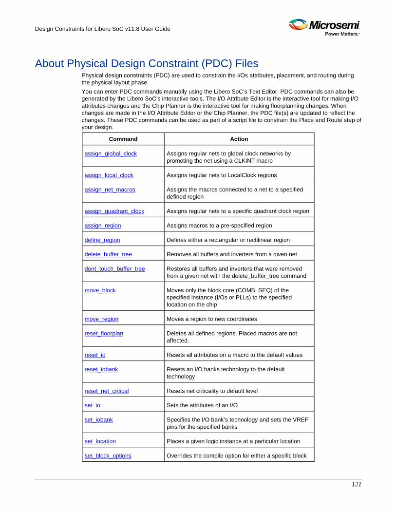
Design Constraints for Libero SoC v11.8 User Guide
121
About Physical Design Constraint (PDC) Files Physical design constraints (PDC) are used to constrain the I/Os attributes, placement, and routing during the physical layout phase. You can enter PDC commands manually using the Libero SoC’s Text Editor. PDC commands can also be generated by the Libero SoC’s interactive tools. The I/O Attribute Editor is the interactive tool for making I/O attributes changes and the Chip Planner is the interactive tool for making floorplanning changes. When changes are made in the I/O Attribute Editor or the Chip Planner, the PDC file(s) are updated to reflect the changes. These PDC commands can be used as part of a script file to constrain the Place and Route step of your design.
Command Action
assign_global_clock Assigns regular nets to global clock networks by promoting the net using a CLKINT macro
assign_local_clock Assigns regular nets to LocalClock regions
assign_net_macros Assigns the macros connected to a net to a specified defined region
assign_quadrant_clock Assigns regular nets to a specific quadrant clock region
assign_region Assigns macros to a pre-specified region
define_region Defines either a rectangular or rectilinear region
delete_buffer_tree Removes all buffers and inverters from a given net
dont_touch_buffer_tree Restores all buffers and inverters that were removed from a given net with the delete_buffer_tree command
move_block Moves only the block core (COMB, SEQ) of the specified instance (I/Os or PLLs) to the specified location on the chip
move_region Moves a region to new coordinates
reset_floorplan Deletes all defined regions. Placed macros are not affected.
reset_io Resets all attributes on a macro to the default values
reset_iobank Resets an I/O banks technology to the default technology
reset_net_critical Resets net criticality to default level
set_io Sets the attributes of an I/O
set_iobank Specifies the I/O bank’s technology and sets the VREF pins for the specified banks
set_location Places a given logic instance at a particular location
set_block_options Overrides the compile option for either a specific block
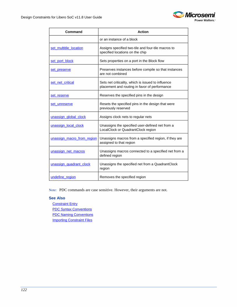
Design Constraints for Libero SoC v11.8 User Guide
122
Command Action
or an instance of a block
set_multitile_location Assigns specified two-tile and four-tile macros to specified locations on the chip
set_port_block Sets properties on a port in the Block flow
set_preserve Preserves instances before compile so that instances are not combined
set_net_critical Sets net criticality, which is issued to influence placement and routing in favor of performance
set_reserve Reserves the specified pins in the design
set_unreserve Resets the specified pins in the design that were previously reserved
unassign_global_clock Assigns clock nets to regular nets
unassign_local_clock Unassigns the specified user-defined net from a LocalClock or QuadrantClock region
unassign_macro_from_region Unassigns macros from a specified region, if they are assigned to that region
unassign_net_macros Unassigns macros connected to a specified net from a defined region
unassign_quadrant_clock Unassigns the specified net from a QuadrantClock region
undefine_region Removes the specified region
Note: PDC commands are case sensitive. However, their arguments are not.
See Also Constraint Entry PDC Syntax Conventions PDC Naming Conventions Importing Constraint Files
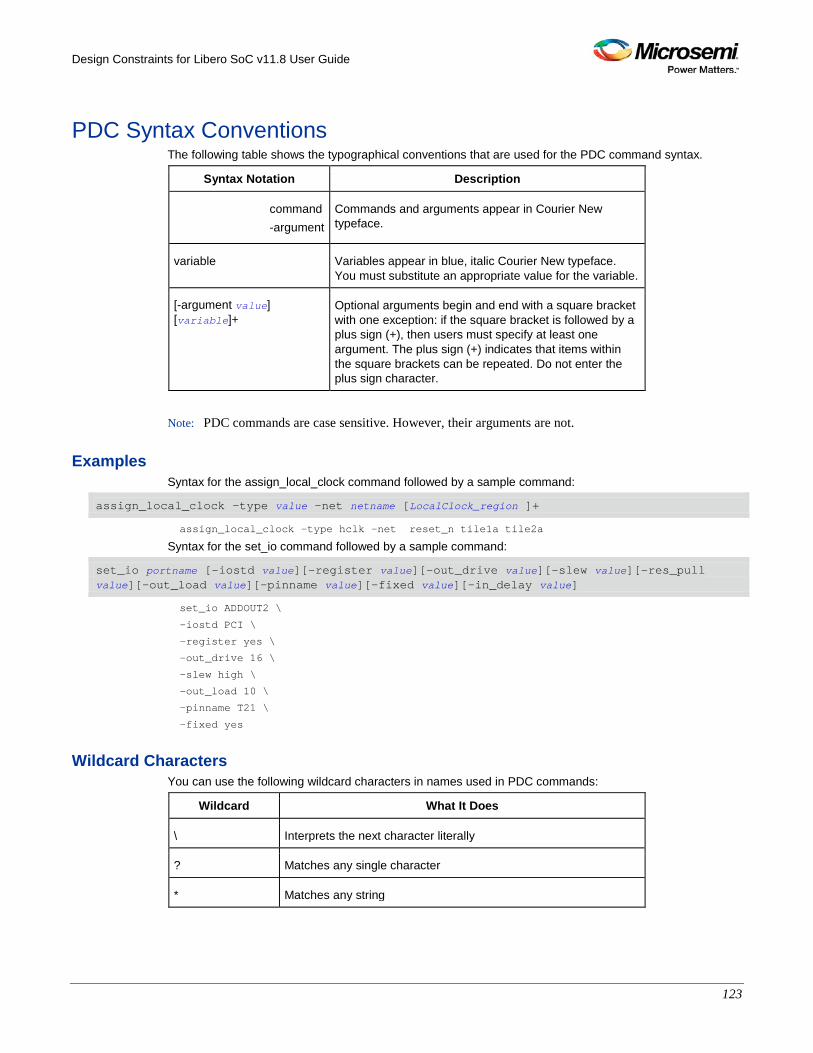
Design Constraints for Libero SoC v11.8 User Guide
123
PDC Syntax Conventions The following table shows the typographical conventions that are used for the PDC command syntax.
Syntax Notation Description
command -argument
Commands and arguments appear in Courier New typeface.
variable Variables appear in blue, italic Courier New typeface. You must substitute an appropriate value for the variable.
[-argument value] [variable]+
Optional arguments begin and end with a square bracket with one exception: if the square bracket is followed by a plus sign (+), then users must specify at least one argument. The plus sign (+) indicates that items within the square brackets can be repeated. Do not enter the plus sign character.
Note: PDC commands are case sensitive. However, their arguments are not.
Examples Syntax for the assign_local_clock command followed by a sample command:
assign_local_clock -type value -net netname [LocalClock_region ]+
assign_local_clock -type hclk -net reset_n tile1a tile2a
Syntax for the set_io command followed by a sample command:
set_io portname [-iostd value][-register value][-out_drive value][-slew value][-res_pull value][-out_load value][-pinname value][-fixed value][-in_delay value]
set_io ADDOUT2 \
-iostd PCI \
-register yes \
-out_drive 16 \
-slew high \
-out_load 10 \
-pinname T21 \
-fixed yes
Wildcard Characters You can use the following wildcard characters in names used in PDC commands:
Wildcard What It Does
\ Interprets the next character literally
? Matches any single character
* Matches any string
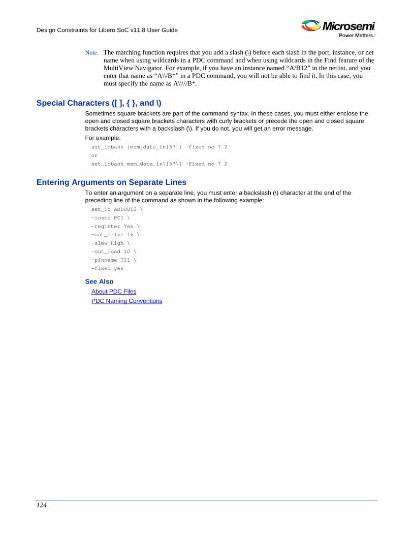
Design Constraints for Libero SoC v11.8 User Guide
124
Note: The matching function requires that you add a slash (\) before each slash in the port, instance, or net name when using wildcards in a PDC command and when using wildcards in the Find feature of the MultiView Navigator. For example, if you have an instance named “A/B12” in the netlist, and you enter that name as “A\\/B*” in a PDC command, you will not be able to find it. In this case, you must specify the name as A\\\\/B*.
Special Characters ([ ], { }, and \) Sometimes square brackets are part of the command syntax. In these cases, you must either enclose the open and closed square brackets characters with curly brackets or precede the open and closed square brackets characters with a backslash (\). If you do not, you will get an error message. For example: set_iobank {mem_data_in[57]} -fixed no 7 2
or
set_iobank mem_data_in\[57\] -fixed no 7 2
Entering Arguments on Separate Lines To enter an argument on a separate line, you must enter a backslash (\) character at the end of the preceding line of the command as shown in the following example: set_io ADDOUT2 \
-iostd PCI \
-register Yes \
-out_drive 16 \
-slew High \
-out_load 10 \
-pinname T21 \
-fixed yes
See Also About PDC Files PDC Naming Conventions
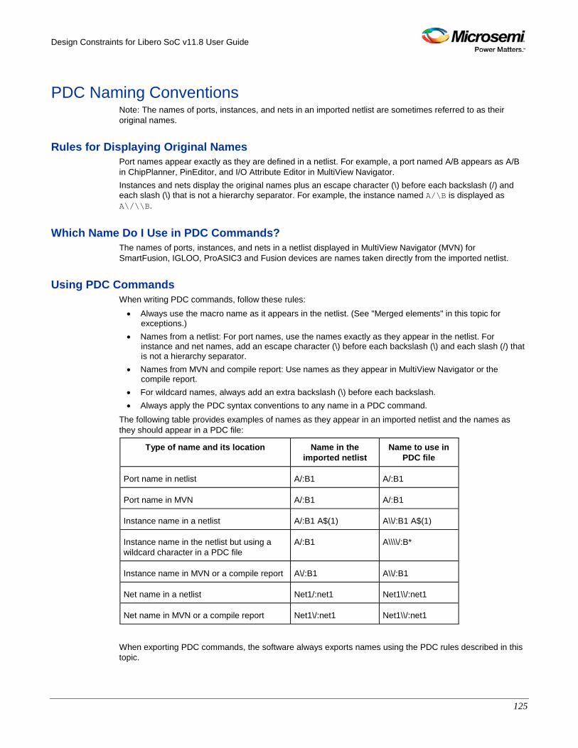
Design Constraints for Libero SoC v11.8 User Guide
125
PDC Naming Conventions Note: The names of ports, instances, and nets in an imported netlist are sometimes referred to as their original names.
Rules for Displaying Original Names Port names appear exactly as they are defined in a netlist. For example, a port named A/B appears as A/B in ChipPlanner, PinEditor, and I/O Attribute Editor in MultiView Navigator. Instances and nets display the original names plus an escape character (\) before each backslash (/) and each slash (\) that is not a hierarchy separator. For example, the instance named A/\B is displayed as A\/\\B.
Which Name Do I Use in PDC Commands? The names of ports, instances, and nets in a netlist displayed in MultiView Navigator (MVN) for SmartFusion, IGLOO, ProASIC3 and Fusion devices are names taken directly from the imported netlist.
Using PDC Commands When writing PDC commands, follow these rules: • Always use the macro name as it appears in the netlist. (See "Merged elements" in this topic for
exceptions.) • Names from a netlist: For port names, use the names exactly as they appear in the netlist. For
instance and net names, add an escape character (\) before each backslash (\) and each slash (/) that is not a hierarchy separator.
• Names from MVN and compile report: Use names as they appear in MultiView Navigator or the compile report.
• For wildcard names, always add an extra backslash (\) before each backslash. • Always apply the PDC syntax conventions to any name in a PDC command.
The following table provides examples of names as they appear in an imported netlist and the names as they should appear in a PDC file:
Type of name and its location Name in the imported netlist
Name to use in PDC file
Port name in netlist A/:B1 A/:B1
Port name in MVN A/:B1 A/:B1
Instance name in a netlist A/:B1 A$(1) A\\/:B1 A$(1)
Instance name in the netlist but using a wildcard character in a PDC file
A/:B1 A\\\\/:B*
Instance name in MVN or a compile report A\/:B1 A\\/:B1
Net name in a netlist Net1/:net1 Net1\\/:net1
Net name in MVN or a compile report Net1\/:net1 Net1\\/:net1
When exporting PDC commands, the software always exports names using the PDC rules described in this topic.
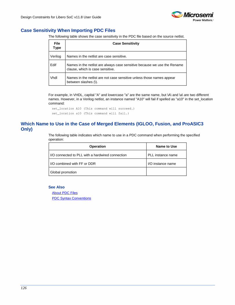
Design Constraints for Libero SoC v11.8 User Guide
126
Case Sensitivity When Importing PDC Files The following table shows the case sensitivity in the PDC file based on the source netlist.
File Type
Case Sensitivity
Verilog Names in the netlist are case sensitive.
Edif Names in the netlist are always case sensitive because we use the Rename clause, which is case sensitive.
Vhdl Names in the netlist are not case sensitive unless those names appear between slashes (\).
For example, in VHDL, capital "A" and lowercase "a" are the same name, but \A\ and \a\ are two different names. However, in a Verilog netlist, an instance named "A10" will fail if spelled as "a10" in the set_location command: set_location A10 (This command will succeed.)
set_location a10 (This command will fail.)
Which Name to Use in the Case of Merged Elements (IGLOO, Fusion, and ProASIC3 Only)
The following table indicates which name to use in a PDC command when performing the specified operation:
Operation Name to Use
I/O connected to PLL with a hardwired connection PLL instance name
I/O combined with FF or DDR I/O instance name
Global promotion
See Also About PDC Files PDC Syntax Conventions
Design Constraints for Libero SoC v11.8 User Guide
127
assign_global_clock PDC command; assigns regular nets to global clock networks by promoting the net using a CLKINT macro.
assign_global_clock -net netname
Arguments -net netname
Specifies the name of the net to promote to a global clock network. The net is promoted using a CLKINT macro, which you can place on a chip-wide clock location.
Supported Families SmartFusion, IGLOO, ProASIC3 and Fusion
Exceptions The assign_global_clock command is not supported in auxiliary PDC files.
Examples assign_global_clock -net globalReset
See Also Assign Net to Global Clock assign_local_clock (IGLOO, Fusion, and ProASIC3) unassign_global_clock PDC Syntax Conventions PDC Naming Conventions PDC Reference
Design Constraints for Libero SoC v11.8 User Guide
128
assign_local_clock PDC command; assigns regular nets to LocalClock regions.
assign_local_clock -net netname-type clock_type clock_region
Arguments -net netname
Specifies the name of the net to assign to a LocalClock region. -type clock_type Specifies the type of region to which the net will be assigned:
Value Description
chip Specifies a LocalClock region driven by a clock rib located on the middle of the chip
quadrant Specifies one of the following: • A QuadrantClock region • A LocalClock region driven by a clock
rib located on the top or bottom of the chip
clock_region
Specifies a LocalClock region. LocalClock regions are defined as one of the following:
• A single spine defined as T# (Top spine) or B# (Bottom spine) • A multi-spine rectangle defined as [T | B]#:[T | B]# Spines are numbered from left to right starting at 1. The maximum spine number is a function of the die selected by the user. Please refer to the examples in this help topic. Local clock uses clock spine resources remaining after global assignment from Input Netlist and PDC constraints. There are six chip-wide and twelve quadrant-wide clock resources per device. You may reserve portions of a clock network (chip-wide or quadrant-wide) for local clocks by assigning clock nets to regions. If there are not enough clock resources to honor all local clock assignments, the Layout command will fail.
Supported Families SmartFusion, IGLOO, ProASIC3 and Fusion Note: You must import the PDC file along with the netlist as a source file because Compile needs to
delete buffers and legalize the netlist. Shared instances between local clocks are supported. Compile will insert buffers to legalize the netlist.
Exceptions • If the net is a clock net, it is demoted to a regular net. You will see an unassign_global_net command
in the PDC file if the net is demoted to a regular net by the compiler and the assignment to local clock failed.
Examples This example assigns the net named localReset to the chip-wide spine T1:
Design Constraints for Libero SoC v11.8 User Guide
129
assign_local_clock -net localReset -type chip T1
This example assigns the net named localReset to the quadrant spines T1, T2, T3, T4, and T5, which span more than one quadrant: assign_local_clock -net localReset -type quadrant T1:T5
This example assigns the net named localReset to the chip-wide spines T1, T2, T3, T4, T5, T6, B1, B2, B3, B4, B4, and B6: assign_local_clock -net localReset -type chip T1:B6
See Also Assign Net to Local Clock unassign_local_clock assign_quadrant_clock PDC Syntax Conventions PDC Naming Conventions PDC Reference
Design Constraints for Libero SoC v11.8 User Guide
130
assign_net_macros PDC command; assigns to a user-defined region all the macros that are connected to a net.
assign_net_macros region_name [net1]+ [-include_driver value]
Arguments region_name
Specifies the name of the region to which you are assigning macros. The region must exist before you use this command. See define_region (rectangular) or define_region (rectilinear). Because the define_region command returns a region object, you can write a simple command such as assign_net_macros [define_region]+ [net]+ net1
You must specify at least one net name. Net names are AFL-level (flattened netlist) names. These names match your netlist names most of the time. When they do not, you must export AFL and use the AFL names. Net names are case insensitive. Hierarchical net names from ADL are not allowed. You can use the following wildcard characters in net names:
Wilcard What It Does
\ Interprets the next character as a non-special character
? Matches any single character
* Matches any string
net1
Specifies whether to add the driver of the net(s) to the region. You can enter one of the following values:
Value Description
Yes Include the driver in the list of macros assigned to the region (default) .
No Do not assign the driver to the region.
Supported Families SmartFusion, IGLOO, ProASIC3 and Fusion
Exceptions • Placed macros (not connected to the net) that are inside the area occupied by the net region are
automatically unplaced. • Net region constraints are internally converted into constraints on macros. PDC export results as a
series of assign_region <region_name> macro1 statements for all the connected macros. • If the region does not have enough space for all of the macros, or if the region constraint is impossible,
the constraint is rejected and a warning message appears in the Log window. • For overlapping regions, the intersection must be at least as big as the overlapping macro count. • If a macro on the net cannot legally be placed in the region, it is not placed and a warning message
appears in the Log window.
Design Constraints for Libero SoC v11.8 User Guide
131
• Net region constraints may result in a single macro being assigned to multiple regions. These net region constraints result in constraining the macro to the intersection of all the regions affected by the constraint.
Examples assign_net_macros cluster_region1 keyin1intZ0Z_62 -include_driver no
See Also Assign Net to Region unassign_net_macros Unassign macros on net from region PDC Syntax Conventions PDC Naming Conventions PDC Reference
Design Constraints for Libero SoC v11.8 User Guide
132
assign_quadrant_clock PDC command; assigns regular nets to a specific quadrant clock region.
assign_quadrant_clock -net netname -quadrant quadrant_clock_region [-fixed value]
Arguments -net netname
Specifies the name of the net to assign to a QuadrantClock region. You must specify a net name that currently exists in the design. -quadrant quadrant_clock_region
Specifies the QuadrantClock region to which the net will be assigned. Each die has four quadrants. QuadrantClock regions are defined as one of the following:
• UL: Upper-Left quadrant
• UR: Upper-Right quadrant
• LL: Lower-Left quadrant
• LR: Lower-Right quadrant
For quadrant clock assignments, regular nets are automatically promoted to clock nets driven by an internal clock driver (CLKINT). There are twelve quadrant-wide clock resources per device. You may reserve portions of a clock network for quadrant clocks by assigning clock nets to regions. If there are not enough clock resources to honor all local clock assignments, the Layout command will fail. -fixed value
Specifies if the specified QuadrantClock region is locked. If you do not want the Global Assigner to remove it, then lock the region. You can enter one of the following values:
Value Description
yes The QuadrantClock region is locked.
no The QuadrantClock region is not locked.
Supported Families SmartFusion, IGLOO, ProASIC3 and Fusion
Exceptions • This command is not supported in auxiliary PDC files. If importing a PDC file that includes this
command, you must import it as a source file.
Examples This example assigns the net named FRAMEN_in to the quadrant clock in the upper-left (UL) quadrant of the chip: assign_quadrant_clock -net FRAMEN_in -quadrant UL
This example assigns the net named STOPN_in to the quadrant clock in the lower-right (LR) quadrant of the chip: assign_quadrant_clock -net STOPN_in -quadrant LR
Design Constraints for Libero SoC v11.8 User Guide
133
This example assigns the net named n32 to the quadrant clock in the lower-right (LR) quadrant of the chip and locks it so that the Global Assigner cannot delete the quadrant region: assign_quadrant_clock -net n32 -quadrant LR -fixed yes
See Also Assign Net to Quadrant Clock unassign_quadrant_clock
PDC Syntax Conventions PDC Naming Conventions PDC Reference
Design Constraints for Libero SoC v11.8 User Guide
134
assign_region PDC command; constrains a set of macros to a specified region.
assign_region region_name [ macro_name]+
Arguments region_name
Specifies the region to which the macros are assigned. The macros are constrained to this region. Because the define_region command returns a region object, you can write a simpler command such as assign_region [define_region]+ [macro_name]+ macro_name
Specifies the macro(s) to assign to the region. You must specify at least one macro name. You can use the following wildcard characters in macro names:
Wildcard What It Does
\ Interprets the next character as a non-special character
? Matches any single character
* Matches any string
Supported Families SmartFusion, IGLOO, ProASIC3 and Fusion
Exceptions • The region must be created before you can assign macros to it. • You can assign only hard macros or their instances to a region. You cannot assign a group name. A
hard macro is a logic cell consisting of one or more silicon modules with locked relative placement. • You can assign a collection of macros by providing a prefix to their names.
Examples In the following example, two macros are assigned to a region: assign_region cluster_region1 des01/G_2722_0_and2 des01/data1_53/U0
In the following example, all macros whose names have the prefix des01/Counter_1 (or all macros whose names match the expression des01/Counter_1/*) are assigned to a region: assign_region User_region2 des01/Counter_1
See Also Assign Macro to Region unassign_macro_from_region
PDC Syntax Conventions PDC Naming Conventions PDC Reference
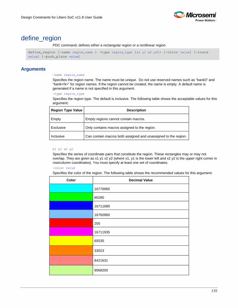
Design Constraints for Libero SoC v11.8 User Guide
135
define_region PDC command; defines either a rectangular region or a rectilinear region.
define_region [-name region_name ] -type region_type [x1 y1 x2 y2]+ [-color value] [-route value] [-push_place value]
Arguments -name region_name
Specifies the region name. The name must be unique. Do not use reserved names such as “bank0” and “bank<N>” for region names. If the region cannot be created, the name is empty. A default name is generated if a name is not specified in this argument. -type region_type
Specifies the region type. The default is inclusive. The following table shows the acceptable values for this argument:
Region Type Value Description
Empty Empty regions cannot contain macros.
Exclusive Only contains macros assigned to the region.
Inclusive Can contain macros both assigned and unassigned to the region.
x1 y1 x2 y2
Specifies the series of coordinate pairs that constitute the region. These rectangles may or may not overlap. They are given as x1 y1 x2 y2 (where x1, y1 is the lower left and x2 y2 is the upper right corner in row/column coordinates). You must specify at least one set of coordinates. -color value
Specifies the color of the region. The following table shows the recommended values for this argument:
Color Decimal Value
16776960
65280
16711680
16760960
255
16711935
65535
33023
8421631
9568200
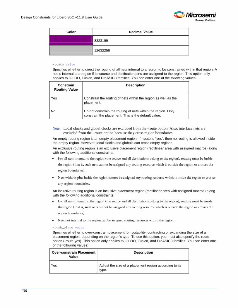
Design Constraints for Libero SoC v11.8 User Guide
136
Color Decimal Value
8323199
12632256
-route value
Specifies whether to direct the routing of all nets internal to a region to be constrained within that region. A net is internal to a region if its source and destination pins are assigned to the region. This option only applies to IGLOO, Fusion, and ProASIC3 families. You can enter one of the following values:
Constrain Routing Value
Description
Yes Constrain the routing of nets within the region as well as the placement.
No Do not constrain the routing of nets within the region. Only constrain the placement. This is the default value.
Note: Local clocks and global clocks are excluded from the -route option. Also, interface nets are
excluded from the –route option because they cross region boundaries. An empty routing region is an empty placement region. If -route is "yes", then no routing is allowed inside the empty region. However, local clocks and globals can cross empty regions. An exclusive routing region is an exclusive placement region (rectilinear area with assigned macros) along with the following additional constraints:
• For all nets internal to the region (the source and all destinations belong to the region), routing must be inside the region (that is, such nets cannot be assigned any routing resource which is outside the region or crosses the region boundaries).
• Nets without pins inside the region cannot be assigned any routing resource which is inside the region or crosses any region boundaries.
An inclusive routing region is an inclusive placement region (rectilinear area with assigned macros) along with the following additional constraints:
• For all nets internal to the region (the source and all destinations belong to the region), routing must be inside the region (that is, such nets cannot be assigned any routing resource which is outside the region or crosses the region boundaries).
• Nets not internal to the region can be assigned routing resources within the region.
-push_place value
Specifies whether to over-constrain placement for routability, contracting or expanding the size of a placement region, depending on the region's type. To use this option, you must also specify the route option (-route yes). This option only applies to IGLOO, Fusion, and ProASIC3 families. You can enter one of the following values:
Over-constrain Placement Value
Description
Yes Adjust the size of a placement region according to its type.
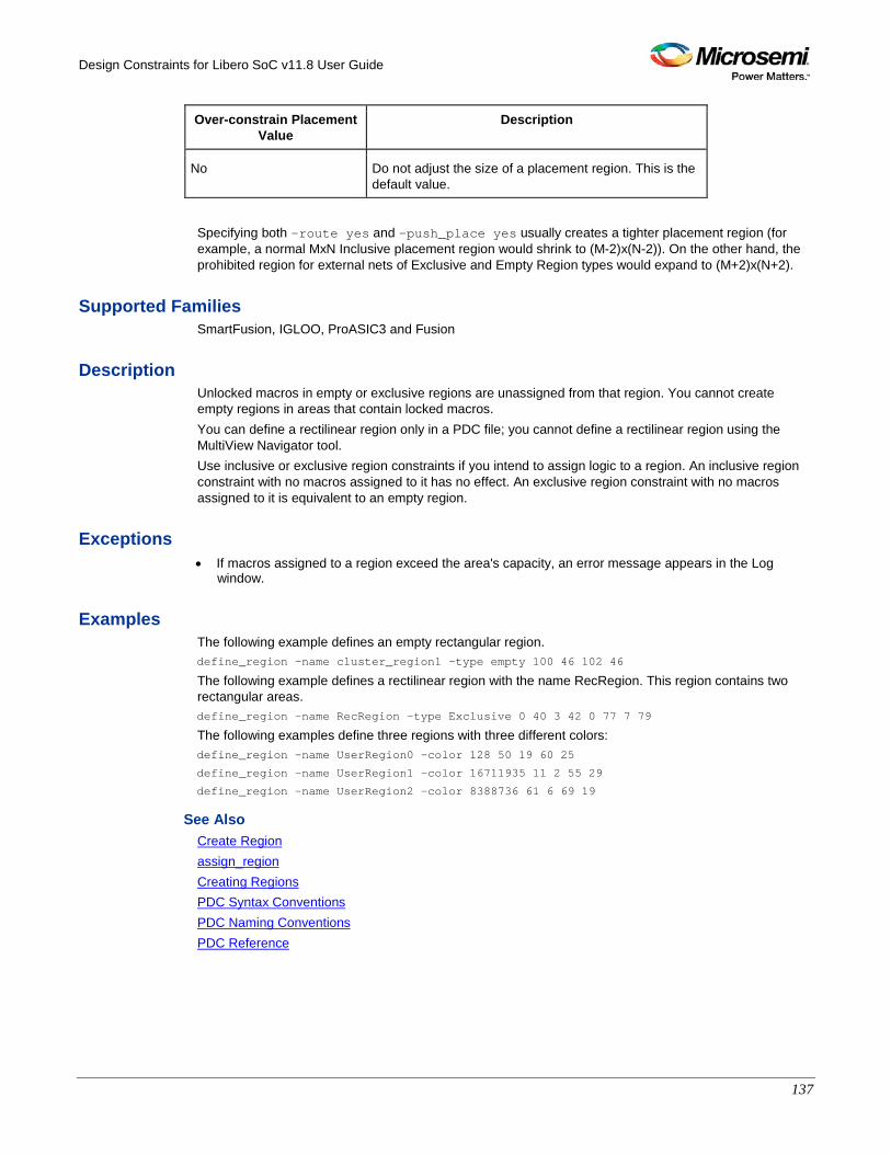
Design Constraints for Libero SoC v11.8 User Guide
137
Over-constrain Placement Value
Description
No Do not adjust the size of a placement region. This is the default value.
Specifying both -route yes and -push_place yes usually creates a tighter placement region (for example, a normal MxN Inclusive placement region would shrink to (M-2)x(N-2)). On the other hand, the prohibited region for external nets of Exclusive and Empty Region types would expand to (M+2)x(N+2).
Supported Families SmartFusion, IGLOO, ProASIC3 and Fusion
Description Unlocked macros in empty or exclusive regions are unassigned from that region. You cannot create empty regions in areas that contain locked macros. You can define a rectilinear region only in a PDC file; you cannot define a rectilinear region using the MultiView Navigator tool. Use inclusive or exclusive region constraints if you intend to assign logic to a region. An inclusive region constraint with no macros assigned to it has no effect. An exclusive region constraint with no macros assigned to it is equivalent to an empty region.
Exceptions • If macros assigned to a region exceed the area's capacity, an error message appears in the Log
window.
Examples The following example defines an empty rectangular region. define_region -name cluster_region1 -type empty 100 46 102 46
The following example defines a rectilinear region with the name RecRegion. This region contains two rectangular areas. define_region -name RecRegion -type Exclusive 0 40 3 42 0 77 7 79
The following examples define three regions with three different colors: define_region -name UserRegion0 -color 128 50 19 60 25
define_region -name UserRegion1 -color 16711935 11 2 55 29
define_region -name UserRegion2 -color 8388736 61 6 69 19
See Also Create Region assign_region Creating Regions PDC Syntax Conventions PDC Naming Conventions PDC Reference
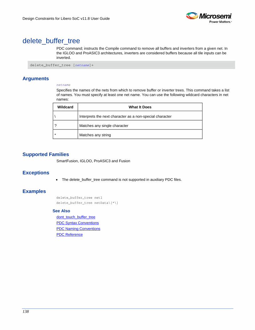
Design Constraints for Libero SoC v11.8 User Guide
138
delete_buffer_tree PDC command; instructs the Compile command to remove all buffers and inverters from a given net. In the IGLOO and ProASIC3 architectures, inverters are considered buffers because all tile inputs can be inverted.
delete_buffer_tree [netname]+
Arguments netname
Specifies the names of the nets from which to remove buffer or inverter trees. This command takes a list of names. You must specify at least one net name. You can use the following wildcard characters in net names:
Wildcard What It Does
\ Interprets the next character as a non-special character
? Matches any single character
* Matches any string
Supported Families SmartFusion, IGLOO, ProASIC3 and Fusion
Exceptions • The delete_buffer_tree command is not supported in auxiliary PDC files.
Examples delete_buffer_tree net1
delete_buffer_tree netData\[*\]
See Also dont_touch_buffer_tree PDC Syntax Conventions PDC Naming Conventions PDC Reference
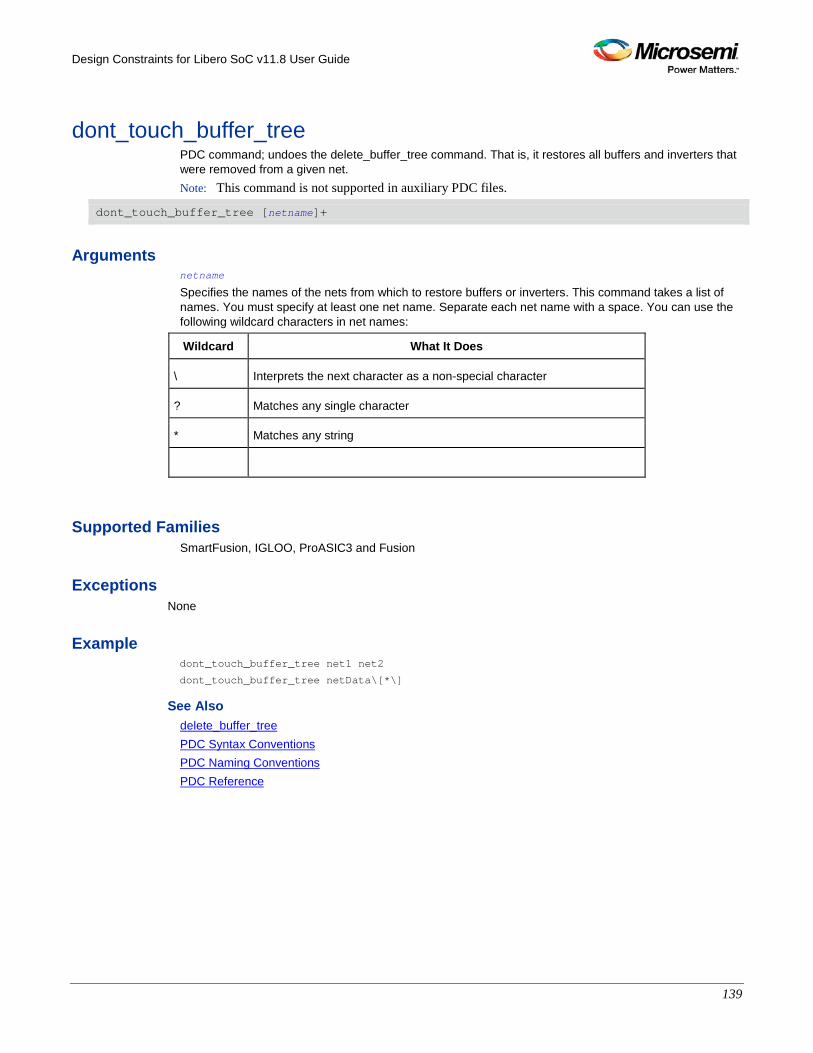
Design Constraints for Libero SoC v11.8 User Guide
139
dont_touch_buffer_tree PDC command; undoes the delete_buffer_tree command. That is, it restores all buffers and inverters that were removed from a given net. Note: This command is not supported in auxiliary PDC files.
dont_touch_buffer_tree [netname]+
Arguments netname
Specifies the names of the nets from which to restore buffers or inverters. This command takes a list of names. You must specify at least one net name. Separate each net name with a space. You can use the following wildcard characters in net names:
Wildcard What It Does
\ Interprets the next character as a non-special character
? Matches any single character
* Matches any string
Supported Families SmartFusion, IGLOO, ProASIC3 and Fusion
Exceptions None
Example dont_touch_buffer_tree net1 net2
dont_touch_buffer_tree netData\[*\]
See Also delete_buffer_tree PDC Syntax Conventions PDC Naming Conventions PDC Reference
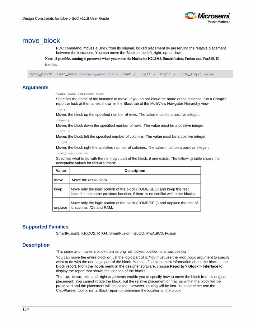
Design Constraints for Libero SoC v11.8 User Guide
140
move_block PDC command; moves a Block from its original, locked placement by preserving the relative placement between the instances. You can move the Block to the left, right, up, or down.
Note: If possible, routing is preserved when you move the blocks for IGLOO, SmartFusion, Fusion and ProASCI3 families.
move_block -inst_name instance_name -up y -down y -left x -right x -non_logic value
Arguments -inst_name instance_name
Specifies the name of the instance to move. If you do not know the name of the instance, run a Compile report or look at the names shown in the Block tab of the MultiView Navigator Hierarchy view. -up y
Moves the block up the specified number of rows. The value must be a positive integer. -down y
Moves the block down the specified number of rows. The value must be a positive integer. -left x
Moves the block left the specified number of columns. The value must be a positive integer. -right x
Moves the block right the specified number of columns. The value must be a positive integer. -non_logic value
Specifies what to do with the non-logic part of the block, if one exists. The following table shows the acceptable values for this argument:
Value Description
move Move the entire block.
keep Move only the logic portion of the block (COMB/SEQ) and keep the rest locked in the same previous location, if there is no conflict with other blocks.
unplace
Move only the logic portion of the block (COMB/SEQ) and unplace the rest of it, such as I/Os and RAM.
Supported Families SmartFusion2, IGLOO2, RTG4, SmartFusion, IGLOO, ProASIC3, Fusion
Description This command moves a block from its original, locked position to a new position. You can move the entire block or just the logic part of it. You must use the -non_logic argument to specify what to do with the non-logic part of the block. You can find placement information about the block in the Block report. From the Tools menu in the designer software, choose Reports > Block > Interface to display the report that shows the location of the blocks. The -up, -down, -left, and -right arguments enable you to specify how to move the block from its original placement. You cannot rotate the block, but the relative placement of macros within the block will be preserved and the placement will be locked. However, routing will be lost. You can either use the ChipPlanner tool or run a Block report to determine the location of the block.
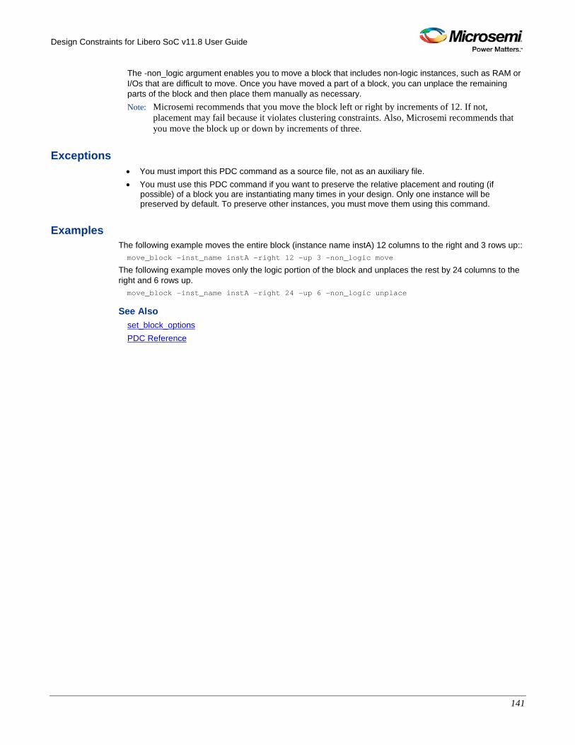
Design Constraints for Libero SoC v11.8 User Guide
141
The -non_logic argument enables you to move a block that includes non-logic instances, such as RAM or I/Os that are difficult to move. Once you have moved a part of a block, you can unplace the remaining parts of the block and then place them manually as necessary. Note: Microsemi recommends that you move the block left or right by increments of 12. If not,
placement may fail because it violates clustering constraints. Also, Microsemi recommends that you move the block up or down by increments of three.
Exceptions • You must import this PDC command as a source file, not as an auxiliary file. • You must use this PDC command if you want to preserve the relative placement and routing (if
possible) of a block you are instantiating many times in your design. Only one instance will be preserved by default. To preserve other instances, you must move them using this command.
Examples The following example moves the entire block (instance name instA) 12 columns to the right and 3 rows up:: move_block -inst_name instA -right 12 -up 3 -non_logic move
The following example moves only the logic portion of the block and unplaces the rest by 24 columns to the right and 6 rows up. move_block -inst_name instA –right 24 –up 6 –non_logic unplace
See Also set_block_options PDC Reference
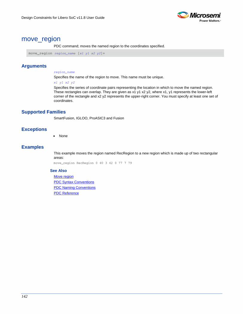
Design Constraints for Libero SoC v11.8 User Guide
142
move_region PDC command; moves the named region to the coordinates specified.
move_region region_name [x1 y1 x2 y2]+
Arguments region_name
Specifies the name of the region to move. This name must be unique. x1 y1 x2 y2
Specifies the series of coordinate pairs representing the location in which to move the named region. These rectangles can overlap. They are given as x1 y1 x2 y2, where x1, y1 represents the lower-left corner of the rectangle and x2 y2 represents the upper-right corner. You must specify at least one set of coordinates.
Supported Families SmartFusion, IGLOO, ProASIC3 and Fusion
Exceptions • None
Examples This example moves the region named RecRegion to a new region which is made up of two rectangular areas: move_region RecRegion 0 40 3 42 0 77 7 79
See Also Move region PDC Syntax Conventions PDC Naming Conventions PDC Reference
Design Constraints for Libero SoC v11.8 User Guide
143
reserve PDC command; reserves the named pins in the current device package.
reserve -pinname "list of package pins"
Arguments -pinname "list of package pins"
Specifies the package pin name(s) to reserve. You can reserve one or more pins.
Supported Families SmartFusion, IGLOO, ProASIC3 and Fusion
Exceptions None
Examples reserve -pinname "F2"
reserve -pinname "F2 B4 B3"
reserve -pinname "124 17"
See Also unreserve
PDC Syntax Conventions PDC Naming Conventions PDC Reference
Design Constraints for Libero SoC v11.8 User Guide
144
reset_floorplan PDC command; deletes all regions.
reset_floorplan
Arguments None
Supported Families SmartFusion, IGLOO, ProASIC3 and Fusion
Exceptions None
Examples reset_floorplan
See Also PDC Syntax Conventions PDC Naming Conventions PDC Reference
Design Constraints for Libero SoC v11.8 User Guide
145
reset_io PDC command; restores all attributes of an I/O macro to its default values. Also, if the port is assigned, it will become unassigned.
reset_io portname -attributes value
Arguments portname
Specifies the port name of the I/O macro to be reset. You can use the following wildcard characters in port names:
Wildcard What It Does
\ Interprets the next character as a non-special character
? Matches any single character
* Matches any string
-attributes value
Preserve or not preserve the I/O attributes during incremental flow. The following table shows the acceptable values for this argument:
Value Description
yes Unassigns all of the I/O attributes and resets them to their default values.
no Unassigns only the port.
Supported Families SmartFusion, IGLOO, ProASIC3 and Fusion
Exceptions None
Examples reset_io a
Resets the I/O macro “a” to the default I/O attributes and unassigns it. reset_io b_*
Resets all I/O macros beginning with "b_" to the default I/O attributes and unassigns them. reset_io b -attributes no
Only unassigns port b from its location.
See Also Reset attributes on an I/O to default settings set_io
PDC Syntax Conventions PDC Naming Conventions
Design Constraints for Libero SoC v11.8 User Guide
146
PDC Reference
reset_iobank PDC command; resets an I/O bank’s technology to the default technology, which is specified using the Designer software in the Device Selection Wizard.
reset_iobank bankname
Arguments bankname
Specifies the I/O bank to be reset to the default technology. For example, for ProASIC3E devices, I/O banks are numbered 0-7 (bank0, bank1,.. bank7).
Supported Families SmartFusion, IGLOO, ProASIC3 and Fusion
Exceptions Any pins that are assigned to the specified I/O bank but are incompatible with the default technology are unassigned.
Examples The following example resets I/O bank 4 to the default technology: reset_iobank bank4
See Also Reset an I/O bank to the default settings set_iobank
PDC Syntax Conventions PDC Naming Conventions PDC Reference
Design Constraints for Libero SoC v11.8 User Guide
147
reset_net_critical PDC command; resets the critical value to its default. Net criticality can vary from 1 to 10, with 1 being the least critical and 10 being the most. The default is 5. Criticality numbers are used in timing driven place-and-route. Increasing a net’s criticality forces place-and-route to keep instances connected to the net as close as possible, at the cost of other (less critical) nets.
reset_net_critical [netname]+
Arguments netname
Specifies the name of the net to be reset to the default critical value. You must specify at least one net name. You can use the following wildcard characters in net names:
Wildcard What It Does
\ Interprets the next character as a non-special character
? Matches any single character
* Matches any string
Supported Families SmartFusion, IGLOO, ProASIC3 and Fusion
Exceptions None
Examples This example resets the net preset_a: reset_net_critical preset_A
See Also Reset net's criticality to default level set_net_critical
PDC Syntax Conventions PDC Naming Conventions PDC Reference
Design Constraints for Libero SoC v11.8 User Guide
148
set_block_options PDC command; overrides the compile option for placement or routing conflicts for an instance of a block.
set_block_options -inst_name instance_name -placement_conflicts value -routing_conflicts value
Arguments -inst_name instance_name
Specifies the block instance name. If you do not know the name of the instance, run a Block Report (Design > Reports > Blocks > Interface) or look at the names shown in the Block tab of the MultiView Navigator Hierarchy view. -placement_conflicts value
Specifies what to do when the software encounters a placement conflict. The following table shows the acceptable values for this argument:
Value Description
error Compile errors out if any instance from a Designer block becomes unplaced or its routing is deleted. This is the default compile option.
resolve If some instances get unplaced for any reason, the non-conflicting elements remaining are also unplaced. Basically, if there are any conflicts, nothing from the block is kept.
keep If some instances get unplaced for any reason, the non-conflicting elements remaining are preserved but not locked. Therefore, the placer can move them into another location if necessary.
lock If some instances get unplaced for any reason, the non-conflicting elements remaining are preserved and locked.
discard Discards any placement from the block, even if there are no conflicts.
-routing_conflicts value
Specifies what to do when the software encounters a routing conflict. The following table shows the acceptable values for this argument:
Value Description
error Compile errors out if any route in any preserved net from a Designer block is deleted.
resolve If a route is removed from a net for any reason, the routing for the non-conflicting nets is also deleted. Basically, if there are any conflicts, no routes from the block are kept.
keep If a route is removed from a net for any reason, the routing for the non-conflicting nets is kept unlocked. Therefore, the router can re-route these nets.
lock If routing is removed from a net for any reason, the routing for the non-conflicting nets is kept as locked, and the router will not change them. This is the default compile option.
Design Constraints for Libero SoC v11.8 User Guide
149
Value Description
discard
Discards any routing from the block, even if there are no conflicts.
Supported Families SmartFusion2, IGLOO2, RTG4, SmartFusion, IGLOO, ProASIC3, Fusion
Description This command enables you to override the compile option for placement or routing conflicts for an instance of a block.
Exceptions You must import this PDC command as a source file, not as an auxiliary file. If placement is discarded, the routing is automatically discarded too.
Examples This example makes the designer software display an error if any instance from a block becomes unplaced or the routing is deleted: set_block_options -inst_name instA -placement_conflicts ERROR -routing_conflicts ERROR
See Also move_block PDC Reference
set_io (SmartFusion2 and IGLOO2) PDC command; sets the attributes of an I/O for SmartFusion2 and IGLOO2 devices. You can use the set_io command to assign an I/O technology, the I/O attributes, place, or lock the I/O at a given pin location. There are three I/O Bank types available in SmartFusion2 and IGLOO2: MSIOD, MSIO and DDRIO.
set_io portname [-iostd value] [-pre_emphasis value] [-lpe value] [-ff_io_state value] [-out_drive value] [-slew value] [-res_pull value] [-schmitt_trigger value] [-input_delay value] [-odt_static value] [-odt_imp value] [-ff_io_avail value] [-register value] [-in_reg value] [-out_reg value] [-en_reg value]
Design Constraints for Libero SoC v11.8 User Guide
150
Arguments portname
Specifies the portname of the I/O macro. -iostd value
Sets the I/O standard for this macro. Choosing a standard allows the software to set other attributes, such as the slew rate and output loading. If the voltage standard used with the I/O is not compatible with other I/Os in the I/O bank, then assigning an I/O standard to a port will invalidate its location and automatically unassign the I/O. The following table shows a list of supported I/Os by Bank type.
MSIOD MSIO DDRIO
- LVTTL -
- LVCMOS33 -
- PCI -
- LVPECL (Input ONLY) -
- LVDS33 -
LVCMOS12 LVCMOS12 LVCMOS12
LVCMOS15 LVCMOS15 LVCMOS15
LVCMOS18 LVCMOS18 LVCMOS18
LVCMOS25 LVCMOS25 LVCMOS25
SSTL2I SSTL2I SSTL2I (DDR1)
- STL2II SSTL2II (DDR1)
SSTL18I SSTL18I SSTL18I (DDR2)
- SSTL18II SSTL18II (DDR2)
HSTLI HSTLI HSTLI
- - HSTLII
- - SSTL15I (DDR3)
- - SSTL15II (DDR3)
- - LPDDRI
- - LPDDRII
LVDS LVDS -
RSDS RSDS -
MINILVDS MINILVDS -
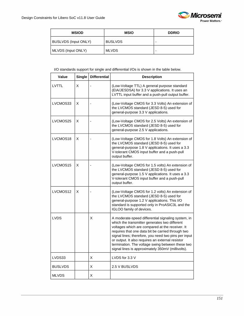
Design Constraints for Libero SoC v11.8 User Guide
151
MSIOD MSIO DDRIO
BUSLVDS (Input ONLY) BUSLVDS -
MLVDS (Input ONLY) MLVDS -
I/O standards support for single and differential I/Os is shown in the table below.
Value Single Differential Description
LVTTL X - (Low-Voltage TTL) A general purpose standard (EIA/JESDSA) for 3.3 V applications. It uses an LVTTL input buffer and a push-pull output buffer.
LVCMOS33 X - (Low-Voltage CMOS for 3.3 Volts) An extension of the LVCMOS standard (JESD 8-5) used for general-purpose 3.3 V applications.
LVCMOS25 X - (Low-Voltage CMOS for 2.5 Volts) An extension of the LVCMOS standard (JESD 8-5) used for general-purpose 2.5 V applications.
LVCMOS18 X - (Low-Voltage CMOS for 1.8 Volts) An extension of the LVCMOS standard (JESD 8-5) used for general-purpose 1.8 V applications. It uses a 3.3 V-tolerant CMOS input buffer and a push-pull output buffer.
LVCMOS15 X - (Low-Voltage CMOS for 1.5 volts) An extension of the LVCMOS standard (JESD 8-5) used for general-purpose 1.5 V applications. It uses a 3.3 V-tolerant CMOS input buffer and a push-pull output buffer.
LVCMOS12 X - (Low-Voltage CMOS for 1.2 volts) An extension of the LVCMOS standard (JESD 8-5) used for general-purpose 1.2 V applications. This I/O standard is supported only in ProASIC3L and the IGLOO family of devices.
LVDS X A moderate-speed differential signaling system, in which the transmitter generates two different voltages which are compared at the receiver. It requires that one data bit be carried through two signal lines; therefore, you need two pins per input or output. It also requires an external resistor termination. The voltage swing between these two signal lines is approximately 350mV (millivolts).
LVDS33 X LVDS for 3.3 V
BUSLVDS X 2.5 V BUSLVDS
MLVDS X
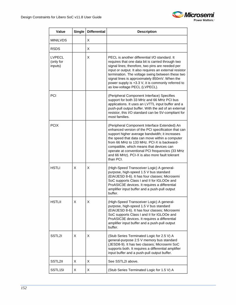
Design Constraints for Libero SoC v11.8 User Guide
152
Value Single Differential Description
MINILVDS X
RSDS X
LVPECL (only for inputs)
X PECL is another differential I/O standard. It requires that one data bit is carried through two signal lines; therefore, two pins are needed per input or output. It also requires an external resistor termination. The voltage swing between these two signal lines is approximately 850mV. When the power supply is +3.3 V, it is commonly referred to as low-voltage PECL (LVPECL).
PCI (Peripheral Component Interface) Specifies support for both 33 MHz and 66 MHz PCI bus applications. It uses an LVTTL input buffer and a push-pull output buffer. With the aid of an external resistor, this I/O standard can be 5V-compliant for most families.
PCIX (Peripheral Component Interface Extended) An enhanced version of the PCI specification that can support higher average bandwidth; it increases the speed that data can move within a computer from 66 MHz to 133 MHz. PCI-X is backward-compatible, which means that devices can operate at conventional PCI frequencies (33 MHz and 66 MHz). PCI-X is also more fault tolerant than PCI.
HSTLI X X (High-Speed Transceiver Logic) A general-purpose, high-speed 1.5 V bus standard (EIA/JESD 8-6). It has four classes; Microsemi SoC supports Class I and II for IGLOOe and ProASIC3E devices. It requires a differential amplifier input buffer and a push-pull output buffer.
HSTLII X X (High-Speed Transceiver Logic) A general-purpose, high-speed 1.5 V bus standard (EIA/JESD 8-6). It has four classes; Microsemi SoC supports Class I and II for IGLOOe and ProASIC3E devices. It requires a differential amplifier input buffer and a push-pull output buffer.
SSTL2I X X (Stub Series Terminated Logic for 2.5 V) A general-purpose 2.5 V memory bus standard (JESD8-9). It has two classes; Microsemi SoC supports both. It requires a differential amplifier input buffer and a push-pull output buffer.
SSTL2II X X See SSTL2I above.
SSTL15I X X (Stub Series Terminated Logic for 1.5 V) A
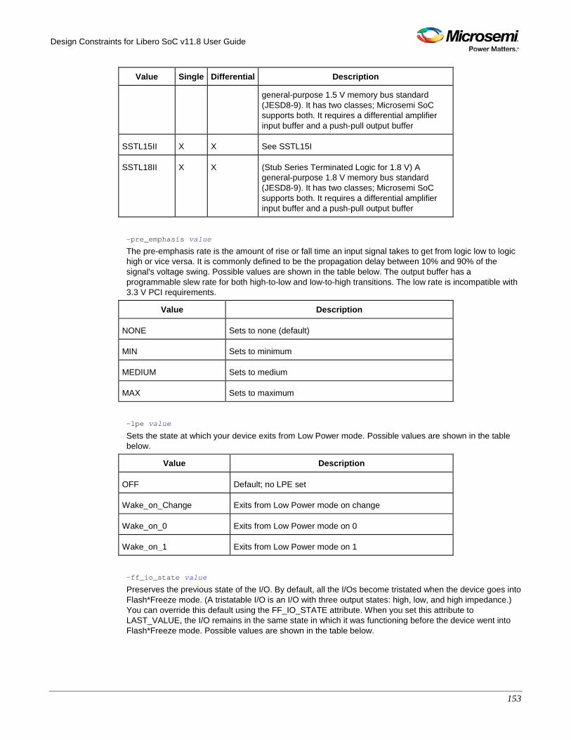
Design Constraints for Libero SoC v11.8 User Guide
153
Value Single Differential Description
general-purpose 1.5 V memory bus standard (JESD8-9). It has two classes; Microsemi SoC supports both. It requires a differential amplifier input buffer and a push-pull output buffer
SSTL15II X X See SSTL15I
SSTL18II X X (Stub Series Terminated Logic for 1.8 V) A general-purpose 1.8 V memory bus standard (JESD8-9). It has two classes; Microsemi SoC supports both. It requires a differential amplifier input buffer and a push-pull output buffer
-pre_emphasis value
The pre-emphasis rate is the amount of rise or fall time an input signal takes to get from logic low to logic high or vice versa. It is commonly defined to be the propagation delay between 10% and 90% of the signal's voltage swing. Possible values are shown in the table below. The output buffer has a programmable slew rate for both high-to-low and low-to-high transitions. The low rate is incompatible with 3.3 V PCI requirements.
Value Description
NONE Sets to none (default)
MIN Sets to minimum
MEDIUM Sets to medium
MAX Sets to maximum
-lpe value
Sets the state at which your device exits from Low Power mode. Possible values are shown in the table below.
Value Description
OFF Default; no LPE set
Wake_on_Change Exits from Low Power mode on change
Wake_on_0 Exits from Low Power mode on 0
Wake_on_1 Exits from Low Power mode on 1
-ff_io_state value
Preserves the previous state of the I/O. By default, all the I/Os become tristated when the device goes into Flash*Freeze mode. (A tristatable I/O is an I/O with three output states: high, low, and high impedance.) You can override this default using the FF_IO_STATE attribute. When you set this attribute to LAST_VALUE, the I/O remains in the same state in which it was functioning before the device went into Flash*Freeze mode. Possible values are shown in the table below.
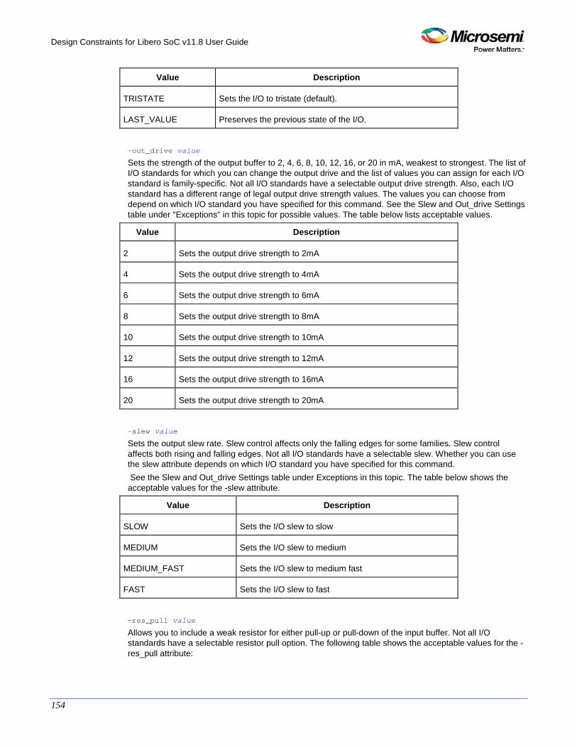
Design Constraints for Libero SoC v11.8 User Guide
154
Value Description
TRISTATE Sets the I/O to tristate (default).
LAST_VALUE Preserves the previous state of the I/O.
-out_drive value
Sets the strength of the output buffer to 2, 4, 6, 8, 10, 12, 16, or 20 in mA, weakest to strongest. The list of I/O standards for which you can change the output drive and the list of values you can assign for each I/O standard is family-specific. Not all I/O standards have a selectable output drive strength. Also, each I/O standard has a different range of legal output drive strength values. The values you can choose from depend on which I/O standard you have specified for this command. See the Slew and Out_drive Settings table under "Exceptions" in this topic for possible values. The table below lists acceptable values.
Value Description
2 Sets the output drive strength to 2mA
4 Sets the output drive strength to 4mA
6 Sets the output drive strength to 6mA
8 Sets the output drive strength to 8mA
10 Sets the output drive strength to 10mA
12 Sets the output drive strength to 12mA
16 Sets the output drive strength to 16mA
20 Sets the output drive strength to 20mA
-slew value
Sets the output slew rate. Slew control affects only the falling edges for some families. Slew control affects both rising and falling edges. Not all I/O standards have a selectable slew. Whether you can use the slew attribute depends on which I/O standard you have specified for this command. See the Slew and Out_drive Settings table under Exceptions in this topic. The table below shows the acceptable values for the -slew attribute.
Value Description
SLOW Sets the I/O slew to slow
MEDIUM Sets the I/O slew to medium
MEDIUM_FAST Sets the I/O slew to medium fast
FAST Sets the I/O slew to fast
-res_pull value
Allows you to include a weak resistor for either pull-up or pull-down of the input buffer. Not all I/O standards have a selectable resistor pull option. The following table shows the acceptable values for the -res_pull attribute:
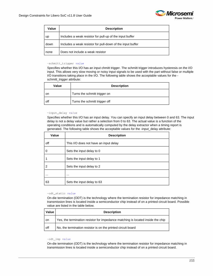
Design Constraints for Libero SoC v11.8 User Guide
155
Value Description
up Includes a weak resistor for pull-up of the input buffer
down Includes a weak resistor for pull-down of the input buffer
none Does not include a weak resistor
-schmitt_trigger value
Specifies whether this I/O has an input chmitt trigger. The schmitt trigger introduces hysteresis on the I/O input. This allows very slow moving or noisy input signals to be used with the part without false or multiple I/O transitions taking place in the I/O. The following table shows the acceptable values for the -schmitt_trigger attribute:
Value Description
on Turns the schmitt trigger on
off Turns the schmitt trigger off
-input_delay value
Specifies whether this I/O has an input delay. You can specify an input delay between 0 and 63. The input delay is not a delay value but rather a selection from 0 to 63. The actual value is a function of the operating conditions and is automatically computed by the delay extractor when a timing report is generated. The following table shows the acceptable values for the -input_delay attribute:
Value Description
off This I/O does not have an input delay
0 Sets the input delay to 0
1 Sets the input delay to 1
2 Sets the input delay to 2
... ...
63 Sets the input delay to 63
-odt_static value
On-die termination (ODT) is the technology where the termination resistor for impedance matching in transmission lines is located inside a semiconductor chip instead of on a printed circuit board. Possible value are listed in the table below.
Value Description
on Yes, the termination resistor for impedance matching is located inside the chip
off No, the termination resistor is on the printed circuit board
-odt_imp value
On-die termination (ODT) is the technology where the termination resistor for impedance matching in transmission lines is located inside a semiconductor chip instead of on a printed circuit board.
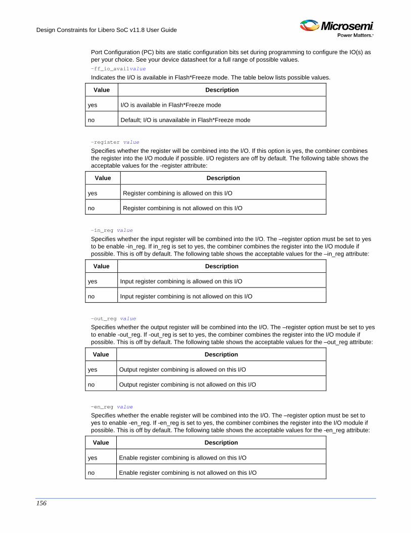
Design Constraints for Libero SoC v11.8 User Guide
156
Port Configuration (PC) bits are static configuration bits set during programming to configure the IO(s) as per your choice. See your device datasheet for a full range of possible values. -ff_io_availvalue
Indicates the I/O is available in Flash*Freeze mode. The table below lists possible values.
Value Description
yes I/O is available in Flash*Freeze mode
no Default; I/O is unavailable in Flash*Freeze mode
-register value
Specifies whether the register will be combined into the I/O. If this option is yes, the combiner combines the register into the I/O module if possible. I/O registers are off by default. The following table shows the acceptable values for the -register attribute:
Value Description
yes Register combining is allowed on this I/O
no Register combining is not allowed on this I/O
-in_reg value
Specifies whether the input register will be combined into the I/O. The –register option must be set to yes to be enable -in_reg. If in_reg is set to yes, the combiner combines the register into the I/O module if possible. This is off by default. The following table shows the acceptable values for the –in_reg attribute:
Value Description
yes Input register combining is allowed on this I/O
no Input register combining is not allowed on this I/O
-out_reg value
Specifies whether the output register will be combined into the I/O. The –register option must be set to yes to enable -out_reg. If -out_reg is set to yes, the combiner combines the register into the I/O module if possible. This is off by default. The following table shows the acceptable values for the –out_reg attribute:
Value Description
yes Output register combining is allowed on this I/O
no Output register combining is not allowed on this I/O
-en_reg value
Specifies whether the enable register will be combined into the I/O. The –register option must be set to yes to enable -en_reg. If -en_reg is set to yes, the combiner combines the register into the I/O module if possible. This is off by default. The following table shows the acceptable values for the -en_reg attribute:
Value Description
yes Enable register combining is allowed on this I/O
no Enable register combining is not allowed on this I/O
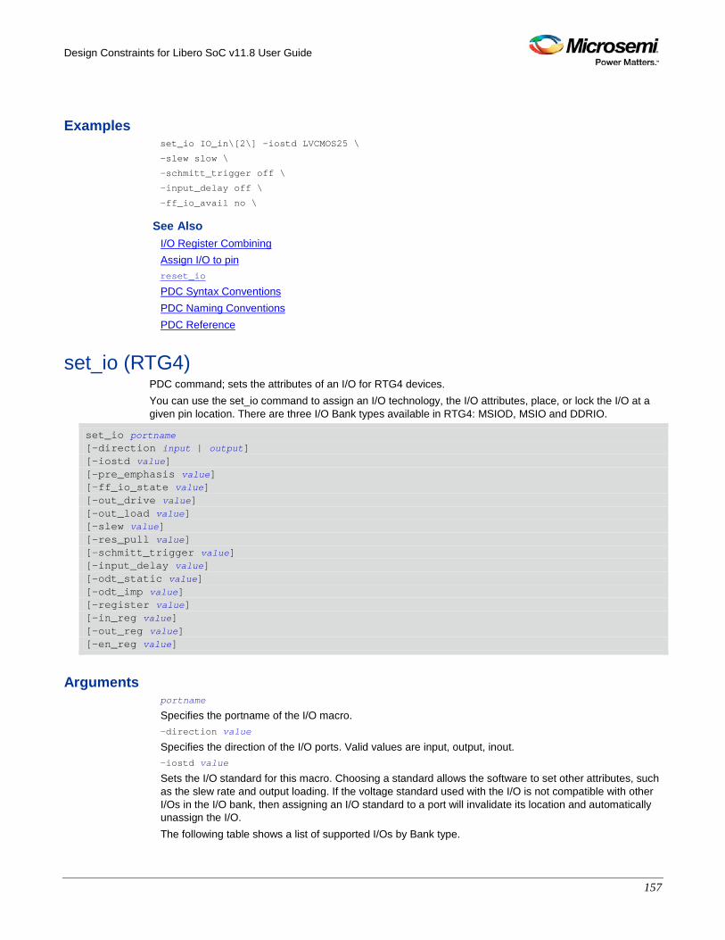
Design Constraints for Libero SoC v11.8 User Guide
157
Examples set_io IO_in\[2\] -iostd LVCMOS25 \
-slew slow \
-schmitt_trigger off \
-input_delay off \
-ff_io_avail no \
See Also I/O Register Combining Assign I/O to pin reset_io
PDC Syntax Conventions PDC Naming Conventions PDC Reference
set_io (RTG4) PDC command; sets the attributes of an I/O for RTG4 devices. You can use the set_io command to assign an I/O technology, the I/O attributes, place, or lock the I/O at a given pin location. There are three I/O Bank types available in RTG4: MSIOD, MSIO and DDRIO.
set_io portname [-direction input | output] [-iostd value] [-pre_emphasis value] [-ff_io_state value] [-out_drive value] [-out_load value] [-slew value] [-res_pull value] [-schmitt_trigger value] [-input_delay value] [-odt_static value] [-odt_imp value] [-register value] [-in_reg value] [-out_reg value] [-en_reg value]
Arguments portname
Specifies the portname of the I/O macro. -direction value
Specifies the direction of the I/O ports. Valid values are input, output, inout. -iostd value
Sets the I/O standard for this macro. Choosing a standard allows the software to set other attributes, such as the slew rate and output loading. If the voltage standard used with the I/O is not compatible with other I/Os in the I/O bank, then assigning an I/O standard to a port will invalidate its location and automatically unassign the I/O. The following table shows a list of supported I/Os by Bank type.
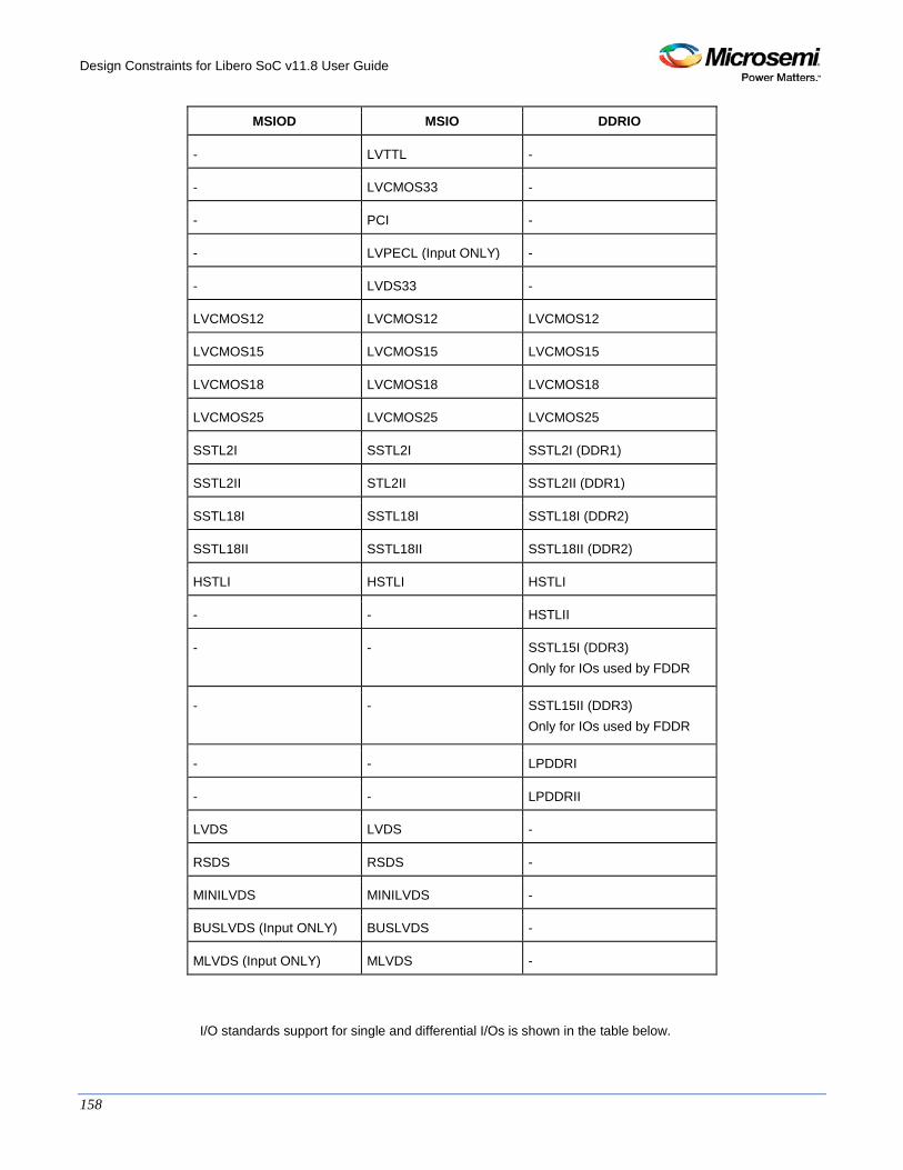
Design Constraints for Libero SoC v11.8 User Guide
158
MSIOD MSIO DDRIO
- LVTTL -
- LVCMOS33 -
- PCI -
- LVPECL (Input ONLY) -
- LVDS33 -
LVCMOS12 LVCMOS12 LVCMOS12
LVCMOS15 LVCMOS15 LVCMOS15
LVCMOS18 LVCMOS18 LVCMOS18
LVCMOS25 LVCMOS25 LVCMOS25
SSTL2I SSTL2I SSTL2I (DDR1)
SSTL2II STL2II SSTL2II (DDR1)
SSTL18I SSTL18I SSTL18I (DDR2)
SSTL18II SSTL18II SSTL18II (DDR2)
HSTLI HSTLI HSTLI
- - HSTLII
- - SSTL15I (DDR3) Only for IOs used by FDDR
- - SSTL15II (DDR3) Only for IOs used by FDDR
- - LPDDRI
- - LPDDRII
LVDS LVDS -
RSDS RSDS -
MINILVDS MINILVDS -
BUSLVDS (Input ONLY) BUSLVDS -
MLVDS (Input ONLY) MLVDS -
I/O standards support for single and differential I/Os is shown in the table below.
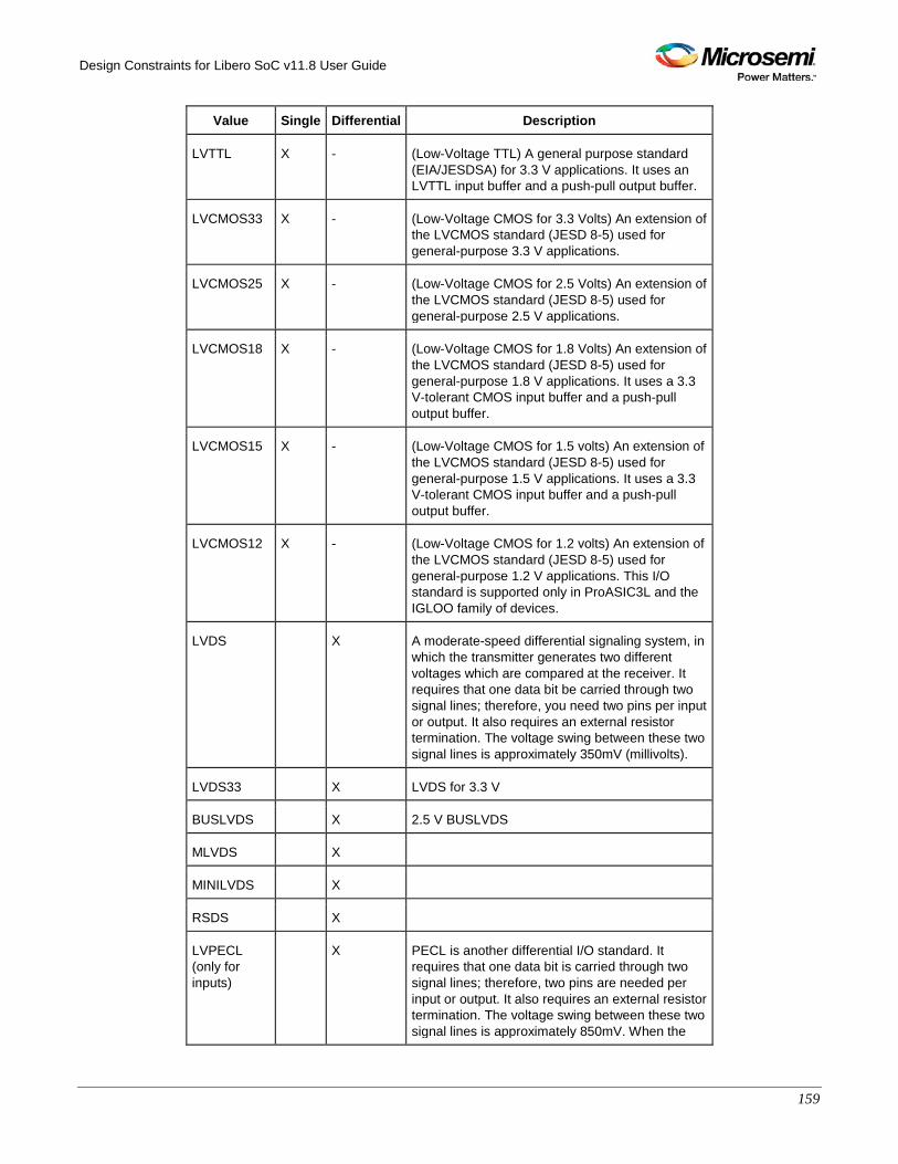
Design Constraints for Libero SoC v11.8 User Guide
159
Value Single Differential Description
LVTTL X - (Low-Voltage TTL) A general purpose standard (EIA/JESDSA) for 3.3 V applications. It uses an LVTTL input buffer and a push-pull output buffer.
LVCMOS33 X - (Low-Voltage CMOS for 3.3 Volts) An extension of the LVCMOS standard (JESD 8-5) used for general-purpose 3.3 V applications.
LVCMOS25 X - (Low-Voltage CMOS for 2.5 Volts) An extension of the LVCMOS standard (JESD 8-5) used for general-purpose 2.5 V applications.
LVCMOS18 X - (Low-Voltage CMOS for 1.8 Volts) An extension of the LVCMOS standard (JESD 8-5) used for general-purpose 1.8 V applications. It uses a 3.3 V-tolerant CMOS input buffer and a push-pull output buffer.
LVCMOS15 X - (Low-Voltage CMOS for 1.5 volts) An extension of the LVCMOS standard (JESD 8-5) used for general-purpose 1.5 V applications. It uses a 3.3 V-tolerant CMOS input buffer and a push-pull output buffer.
LVCMOS12 X - (Low-Voltage CMOS for 1.2 volts) An extension of the LVCMOS standard (JESD 8-5) used for general-purpose 1.2 V applications. This I/O standard is supported only in ProASIC3L and the IGLOO family of devices.
LVDS X A moderate-speed differential signaling system, in which the transmitter generates two different voltages which are compared at the receiver. It requires that one data bit be carried through two signal lines; therefore, you need two pins per input or output. It also requires an external resistor termination. The voltage swing between these two signal lines is approximately 350mV (millivolts).
LVDS33 X LVDS for 3.3 V
BUSLVDS X 2.5 V BUSLVDS
MLVDS X
MINILVDS X
RSDS X
LVPECL (only for inputs)
X PECL is another differential I/O standard. It requires that one data bit is carried through two signal lines; therefore, two pins are needed per input or output. It also requires an external resistor termination. The voltage swing between these two signal lines is approximately 850mV. When the
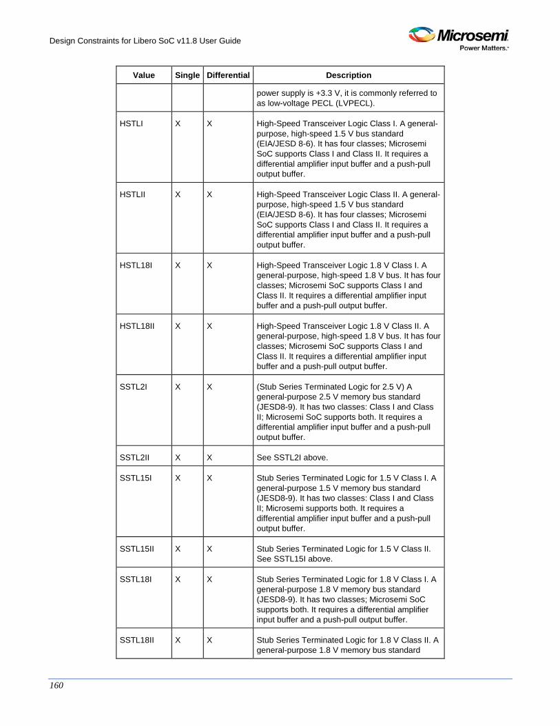
Design Constraints for Libero SoC v11.8 User Guide
160
Value Single Differential Description
power supply is +3.3 V, it is commonly referred to as low-voltage PECL (LVPECL).
HSTLI X X High-Speed Transceiver Logic Class I. A general-purpose, high-speed 1.5 V bus standard (EIA/JESD 8-6). It has four classes; Microsemi SoC supports Class I and Class II. It requires a differential amplifier input buffer and a push-pull output buffer.
HSTLII X X High-Speed Transceiver Logic Class II. A general-purpose, high-speed 1.5 V bus standard (EIA/JESD 8-6). It has four classes; Microsemi SoC supports Class I and Class II. It requires a differential amplifier input buffer and a push-pull output buffer.
HSTL18I X X High-Speed Transceiver Logic 1.8 V Class I. A general-purpose, high-speed 1.8 V bus. It has four classes; Microsemi SoC supports Class I and Class II. It requires a differential amplifier input buffer and a push-pull output buffer.
HSTL18II X X High-Speed Transceiver Logic 1.8 V Class II. A general-purpose, high-speed 1.8 V bus. It has four classes; Microsemi SoC supports Class I and Class II. It requires a differential amplifier input buffer and a push-pull output buffer.
SSTL2I X X (Stub Series Terminated Logic for 2.5 V) A general-purpose 2.5 V memory bus standard (JESD8-9). It has two classes: Class I and Class II; Microsemi SoC supports both. It requires a differential amplifier input buffer and a push-pull output buffer.
SSTL2II X X See SSTL2I above.
SSTL15I X X Stub Series Terminated Logic for 1.5 V Class I. A general-purpose 1.5 V memory bus standard (JESD8-9). It has two classes: Class I and Class II; Microsemi supports both. It requires a differential amplifier input buffer and a push-pull output buffer.
SSTL15II X X Stub Series Terminated Logic for 1.5 V Class II. See SSTL15I above.
SSTL18I X X Stub Series Terminated Logic for 1.8 V Class I. A general-purpose 1.8 V memory bus standard (JESD8-9). It has two classes; Microsemi SoC supports both. It requires a differential amplifier input buffer and a push-pull output buffer.
SSTL18II X X Stub Series Terminated Logic for 1.8 V Class II. A general-purpose 1.8 V memory bus standard
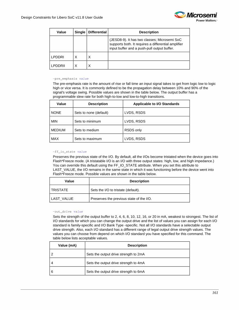
Design Constraints for Libero SoC v11.8 User Guide
161
Value Single Differential Description
(JESD8-9). It has two classes; Microsemi SoC supports both. It requires a differential amplifier input buffer and a push-pull output buffer.
LPDDRI X X
LPDDRII X X
-pre_emphasis value
The pre-emphasis rate is the amount of rise or fall time an input signal takes to get from logic low to logic high or vice versa. It is commonly defined to be the propagation delay between 10% and 90% of the signal's voltage swing. Possible values are shown in the table below. The output buffer has a programmable slew rate for both high-to-low and low-to-high transitions.
Value Description Applicable to I/O Standards
NONE Sets to none (default) LVDS, RSDS
MIN Sets to minimum LVDS, RSDS
MEDIUM Sets to medium RSDS only
MAX Sets to maximum LVDS, RSDS
-ff_io_state value
Preserves the previous state of the I/O. By default, all the I/Os become tristated when the device goes into Flash*Freeze mode. (A tristatable I/O is an I/O with three output states: high, low, and high impedance.) You can override this default using the FF_IO_STATE attribute. When you set this attribute to LAST_VALUE, the I/O remains in the same state in which it was functioning before the device went into Flash*Freeze mode. Possible values are shown in the table below.
Value Description
TRISTATE Sets the I/O to tristate (default).
LAST_VALUE Preserves the previous state of the I/O.
-out_drive value
Sets the strength of the output buffer to 2, 4, 6, 8, 10, 12, 16, or 20 in mA, weakest to strongest. The list of I/O standards for which you can change the output drive and the list of values you can assign for each I/O standard is family-specific and I/O Bank Type -specific. Not all I/O standards have a selectable output drive strength. Also, each I/O standard has a different range of legal output drive strength values. The values you can choose from depend on which I/O standard you have specified for this command. The table below lists acceptable values.
Value (mA) Description
2 Sets the output drive strength to 2mA
4 Sets the output drive strength to 4mA
6 Sets the output drive strength to 6mA
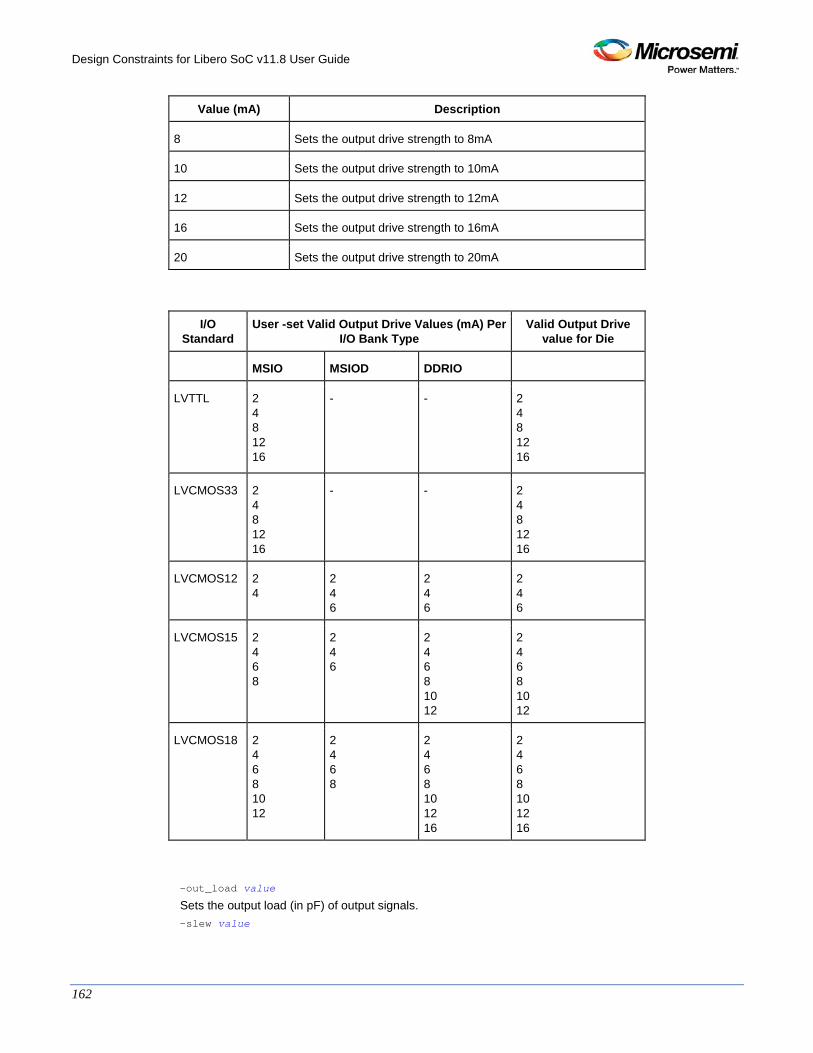
Design Constraints for Libero SoC v11.8 User Guide
162
Value (mA) Description
8 Sets the output drive strength to 8mA
10 Sets the output drive strength to 10mA
12 Sets the output drive strength to 12mA
16 Sets the output drive strength to 16mA
20 Sets the output drive strength to 20mA
I/O Standard
User -set Valid Output Drive Values (mA) Per I/O Bank Type
Valid Output Drive value for Die
MSIO MSIOD DDRIO
LVTTL 2 4 8 12 16
- - 2 4 8 12 16
LVCMOS33 2 4 8 12 16
- - 2 4 8 12 16
LVCMOS12 2 4
2 4 6
2 4 6
2 4 6
LVCMOS15 2 4 6 8
2 4 6
2 4 6 8 10 12
2 4 6 8 10 12
LVCMOS18 2 4 6 8 10 12
2 4 6 8
2 4 6 8 10 12 16
2 4 6 8 10 12 16
-out_load value
Sets the output load (in pF) of output signals. -slew value
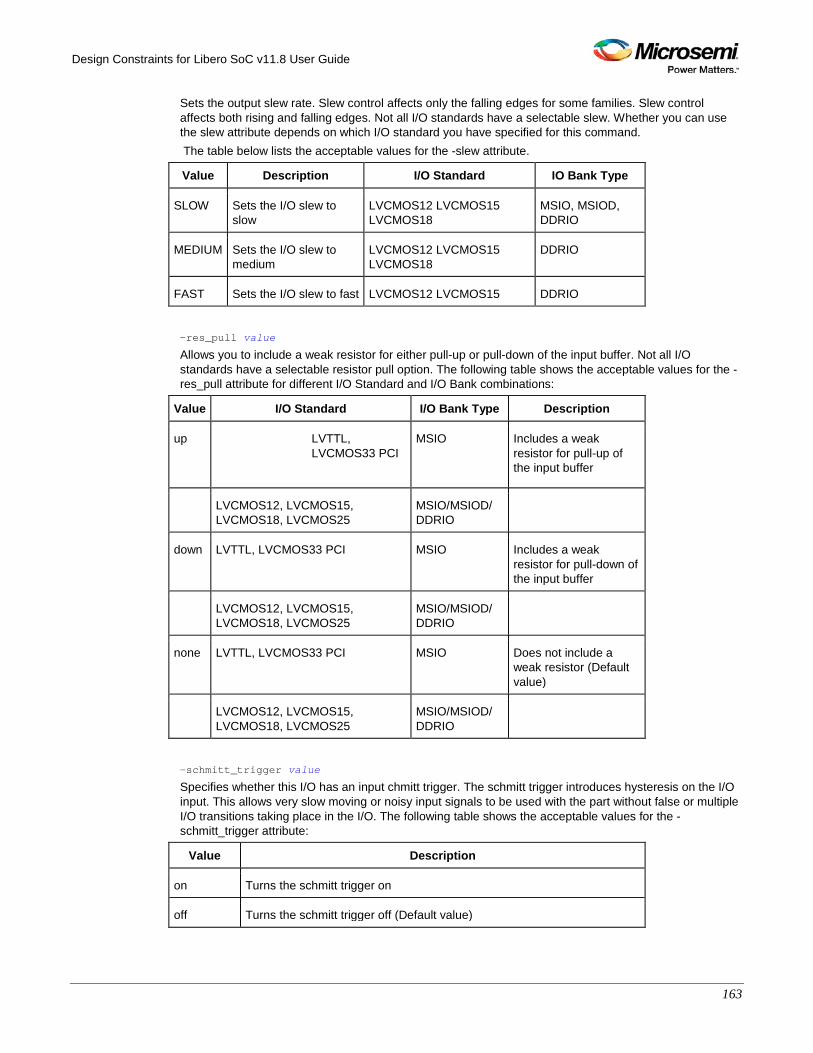
Design Constraints for Libero SoC v11.8 User Guide
163
Sets the output slew rate. Slew control affects only the falling edges for some families. Slew control affects both rising and falling edges. Not all I/O standards have a selectable slew. Whether you can use the slew attribute depends on which I/O standard you have specified for this command. The table below lists the acceptable values for the -slew attribute.
Value Description I/O Standard IO Bank Type
SLOW Sets the I/O slew to slow
LVCMOS12 LVCMOS15 LVCMOS18
MSIO, MSIOD, DDRIO
MEDIUM Sets the I/O slew to medium
LVCMOS12 LVCMOS15 LVCMOS18
DDRIO
FAST Sets the I/O slew to fast LVCMOS12 LVCMOS15 DDRIO
-res_pull value
Allows you to include a weak resistor for either pull-up or pull-down of the input buffer. Not all I/O standards have a selectable resistor pull option. The following table shows the acceptable values for the -res_pull attribute for different I/O Standard and I/O Bank combinations:
Value I/O Standard I/O Bank Type Description
up LVTTL, LVCMOS33 PCI
MSIO Includes a weak resistor for pull-up of the input buffer
LVCMOS12, LVCMOS15, LVCMOS18, LVCMOS25
MSIO/MSIOD/ DDRIO
down LVTTL, LVCMOS33 PCI MSIO Includes a weak resistor for pull-down of the input buffer
LVCMOS12, LVCMOS15, LVCMOS18, LVCMOS25
MSIO/MSIOD/ DDRIO
none LVTTL, LVCMOS33 PCI MSIO Does not include a weak resistor (Default value)
LVCMOS12, LVCMOS15, LVCMOS18, LVCMOS25
MSIO/MSIOD/ DDRIO
-schmitt_trigger value
Specifies whether this I/O has an input chmitt trigger. The schmitt trigger introduces hysteresis on the I/O input. This allows very slow moving or noisy input signals to be used with the part without false or multiple I/O transitions taking place in the I/O. The following table shows the acceptable values for the -schmitt_trigger attribute:
Value Description
on Turns the schmitt trigger on
off Turns the schmitt trigger off (Default value)
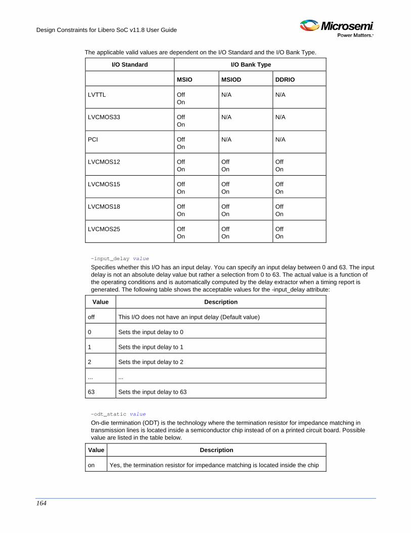
Design Constraints for Libero SoC v11.8 User Guide
164
The applicable valid values are dependent on the I/O Standard and the I/O Bank Type.
I/O Standard I/O Bank Type
MSIO MSIOD DDRIO
LVTTL Off On
N/A N/A
LVCMOS33 Off On
N/A N/A
PCI Off On
N/A N/A
LVCMOS12 Off On
Off On
Off On
LVCMOS15 Off On
Off On
Off On
LVCMOS18 Off On
Off On
Off On
LVCMOS25 Off On
Off On
Off On
-input_delay value
Specifies whether this I/O has an input delay. You can specify an input delay between 0 and 63. The input delay is not an absolute delay value but rather a selection from 0 to 63. The actual value is a function of the operating conditions and is automatically computed by the delay extractor when a timing report is generated. The following table shows the acceptable values for the -input_delay attribute:
Value Description
off This I/O does not have an input delay (Default value)
0 Sets the input delay to 0
1 Sets the input delay to 1
2 Sets the input delay to 2
... ...
63 Sets the input delay to 63
-odt_static value
On-die termination (ODT) is the technology where the termination resistor for impedance matching in transmission lines is located inside a semiconductor chip instead of on a printed circuit board. Possible value are listed in the table below.
Value Description
on Yes, the termination resistor for impedance matching is located inside the chip
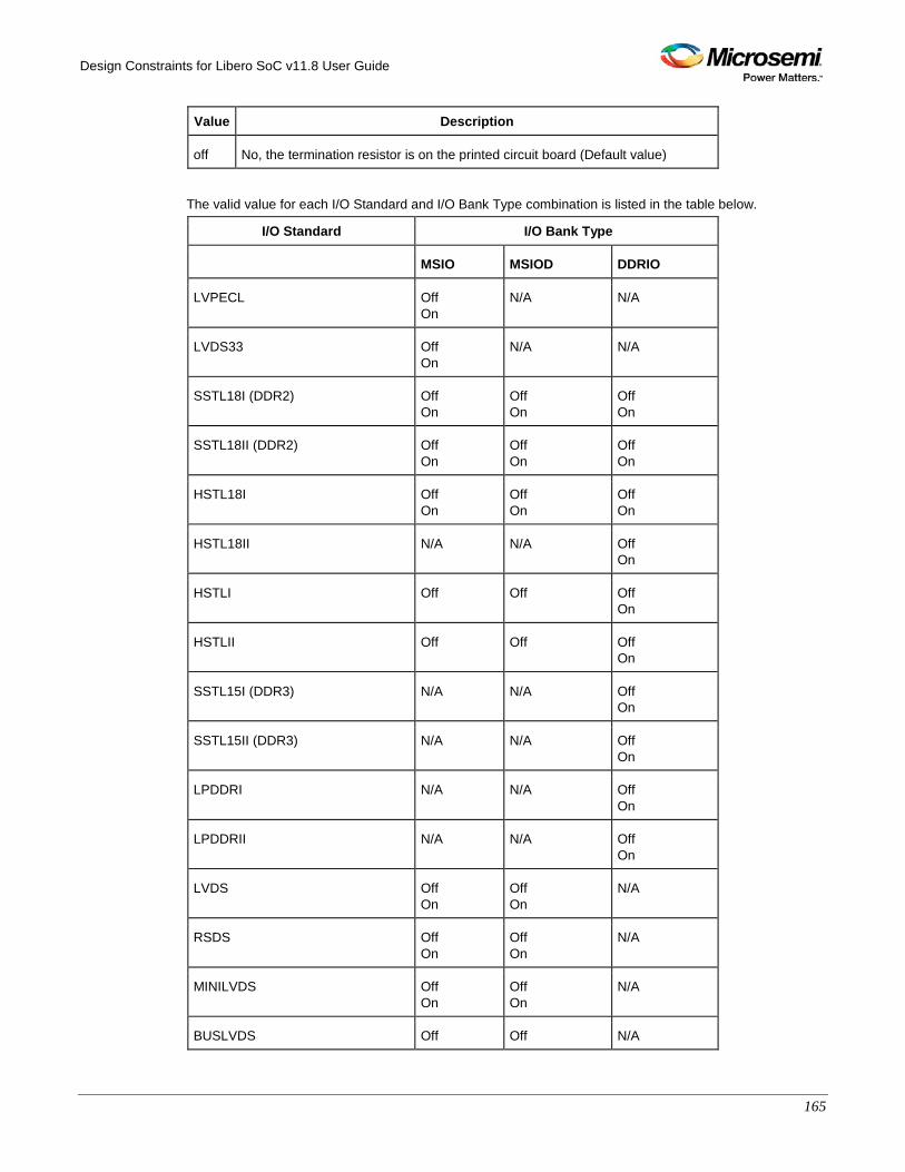
Design Constraints for Libero SoC v11.8 User Guide
165
Value Description
off No, the termination resistor is on the printed circuit board (Default value)
The valid value for each I/O Standard and I/O Bank Type combination is listed in the table below.
I/O Standard I/O Bank Type
MSIO MSIOD DDRIO
LVPECL Off On
N/A N/A
LVDS33 Off On
N/A N/A
SSTL18I (DDR2) Off On
Off On
Off On
SSTL18II (DDR2) Off On
Off On
Off On
HSTL18I Off On
Off On
Off On
HSTL18II N/A N/A Off On
HSTLI Off Off Off On
HSTLII Off Off Off On
SSTL15I (DDR3) N/A N/A Off On
SSTL15II (DDR3) N/A N/A Off On
LPDDRI N/A N/A Off On
LPDDRII N/A N/A Off On
LVDS Off On
Off On
N/A
RSDS Off On
Off On
N/A
MINILVDS Off On
Off On
N/A
BUSLVDS Off Off N/A
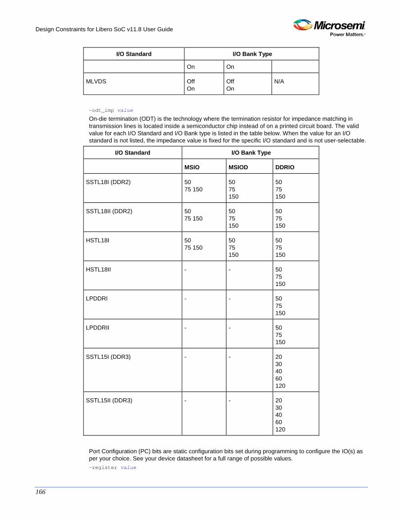
Design Constraints for Libero SoC v11.8 User Guide
166
I/O Standard I/O Bank Type
On On
MLVDS Off On
Off On
N/A
-odt_imp value
On-die termination (ODT) is the technology where the termination resistor for impedance matching in transmission lines is located inside a semiconductor chip instead of on a printed circuit board. The valid value for each I/O Standard and I/O Bank type is listed in the table below. When the value for an I/O standard is not listed, the impedance value is fixed for the specific I/O standard and is not user-selectable.
I/O Standard I/O Bank Type
MSIO MSIOD DDRIO
SSTL18I (DDR2) 50 75 150
50 75 150
50 75 150
SSTL18II (DDR2) 50 75 150
50 75 150
50 75 150
HSTL18I 50 75 150
50 75 150
50 75 150
HSTL18II - - 50 75 150
LPDDRI - - 50 75 150
LPDDRII - - 50 75 150
SSTL15I (DDR3) - - 20 30 40 60 120
SSTL15II (DDR3) - - 20 30 40 60 120
Port Configuration (PC) bits are static configuration bits set during programming to configure the IO(s) as per your choice. See your device datasheet for a full range of possible values. -register value
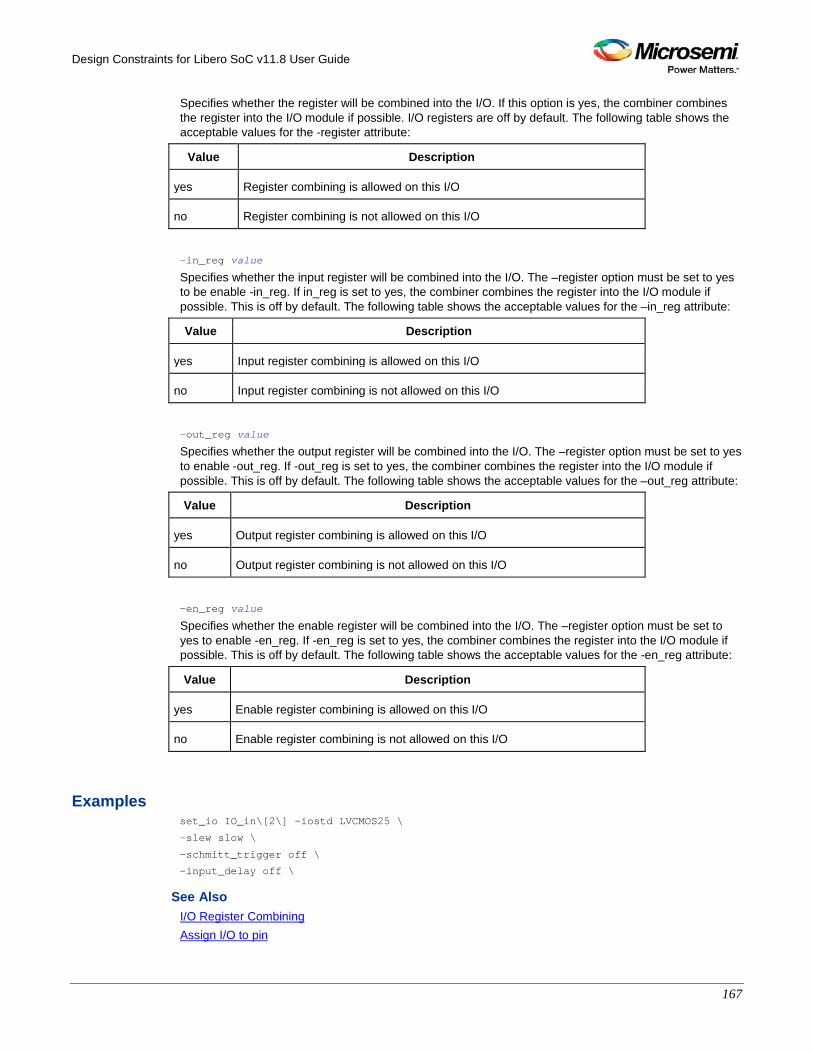
Design Constraints for Libero SoC v11.8 User Guide
167
Specifies whether the register will be combined into the I/O. If this option is yes, the combiner combines the register into the I/O module if possible. I/O registers are off by default. The following table shows the acceptable values for the -register attribute:
Value Description
yes Register combining is allowed on this I/O
no Register combining is not allowed on this I/O
-in_reg value
Specifies whether the input register will be combined into the I/O. The –register option must be set to yes to be enable -in_reg. If in_reg is set to yes, the combiner combines the register into the I/O module if possible. This is off by default. The following table shows the acceptable values for the –in_reg attribute:
Value Description
yes Input register combining is allowed on this I/O
no Input register combining is not allowed on this I/O
-out_reg value
Specifies whether the output register will be combined into the I/O. The –register option must be set to yes to enable -out_reg. If -out_reg is set to yes, the combiner combines the register into the I/O module if possible. This is off by default. The following table shows the acceptable values for the –out_reg attribute:
Value Description
yes Output register combining is allowed on this I/O
no Output register combining is not allowed on this I/O
-en_reg value
Specifies whether the enable register will be combined into the I/O. The –register option must be set to yes to enable -en_reg. If -en_reg is set to yes, the combiner combines the register into the I/O module if possible. This is off by default. The following table shows the acceptable values for the -en_reg attribute:
Value Description
yes Enable register combining is allowed on this I/O
no Enable register combining is not allowed on this I/O
Examples set_io IO_in\[2\] -iostd LVCMOS25 \
-slew slow \
-schmitt_trigger off \
-input_delay off \
See Also I/O Register Combining Assign I/O to pin
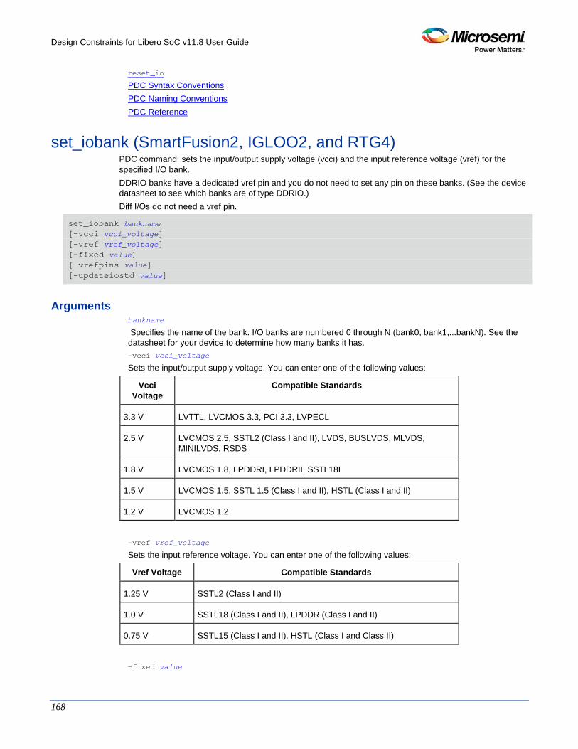
Design Constraints for Libero SoC v11.8 User Guide
168
reset_io
PDC Syntax Conventions PDC Naming Conventions PDC Reference
set_iobank (SmartFusion2, IGLOO2, and RTG4) PDC command; sets the input/output supply voltage (vcci) and the input reference voltage (vref) for the specified I/O bank. DDRIO banks have a dedicated vref pin and you do not need to set any pin on these banks. (See the device datasheet to see which banks are of type DDRIO.) Diff I/Os do not need a vref pin.
set_iobank bankname [-vcci vcci_voltage] [-vref vref_voltage] [-fixed value] [-vrefpins value] [-updateiostd value]
Arguments bankname
Specifies the name of the bank. I/O banks are numbered 0 through N (bank0, bank1,...bankN). See the datasheet for your device to determine how many banks it has. -vcci vcci_voltage
Sets the input/output supply voltage. You can enter one of the following values:
Vcci Voltage
Compatible Standards
3.3 V LVTTL, LVCMOS 3.3, PCI 3.3, LVPECL
2.5 V LVCMOS 2.5, SSTL2 (Class I and II), LVDS, BUSLVDS, MLVDS, MINILVDS, RSDS
1.8 V LVCMOS 1.8, LPDDRI, LPDDRII, SSTL18I
1.5 V LVCMOS 1.5, SSTL 1.5 (Class I and II), HSTL (Class I and II)
1.2 V LVCMOS 1.2
-vref vref_voltage
Sets the input reference voltage. You can enter one of the following values:
Vref Voltage Compatible Standards
1.25 V SSTL2 (Class I and II)
1.0 V SSTL18 (Class I and II), LPDDR (Class I and II)
0.75 V SSTL15 (Class I and II), HSTL (Class I and Class II)
-fixed value
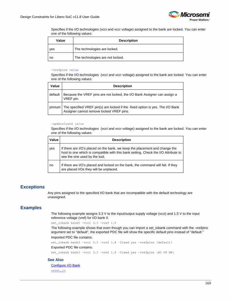
Design Constraints for Libero SoC v11.8 User Guide
169
Specifies if the I/O technologies (vcci and vccr voltage) assigned to the bank are locked. You can enter one of the following values:
Value Description
yes The technologies are locked.
no The technologies are not locked.
-vrefpins value
Specifies if the I/O technologies (vcci and vccr voltage) assigned to the bank are locked. You can enter one of the following values:
Value Description
default Because the VREF pins are not locked, the I/O Bank Assigner can assign a VREF pin.
pinnum The specified VREF pin(s) are locked if the -fixed option is yes. The I/O Bank Assigner cannot remove locked VREF pins.
-updateiostd value
Specifies if the I/O technologies (vcci and vccr voltage) assigned to the bank are locked. You can enter one of the following values:
Value Description
yes If there are I/O's placed on the bank, we keep the placement and change the host to one which is compatible with this bank setting. Check the I/O Attribute to see the one used by the tool.
no If there are I/O's placed and locked on the bank, the command will fail. If they are placed I/Os they will be unplaced.
Exceptions Any pins assigned to the specified I/O bank that are incompatible with the default technology are unassigned.
Examples The following example assigns 3.3 V to the input/output supply voltage (vcci) and 1.5 V to the input reference voltage (vref) for I/O bank 0. set_iobank bank0 -vcci 3.3 -vref 1.5
The following example shows that even though you can import a set_iobank command with the -vrefpins argument set to "default", the exported PDC file will show the specific default pins instead of "default." Imported PDC file contains: set_iobank bank3 -vcci 3.3 -vref 1.8 -fixed yes -vrefpins {default}
Exported PDC file contains: set_iobank bank3 -vcci 3.3 -vref 1.8 -fixed yes -vrefpins {N3 P8 M8}
See Also Configure I/O Bank reset_io
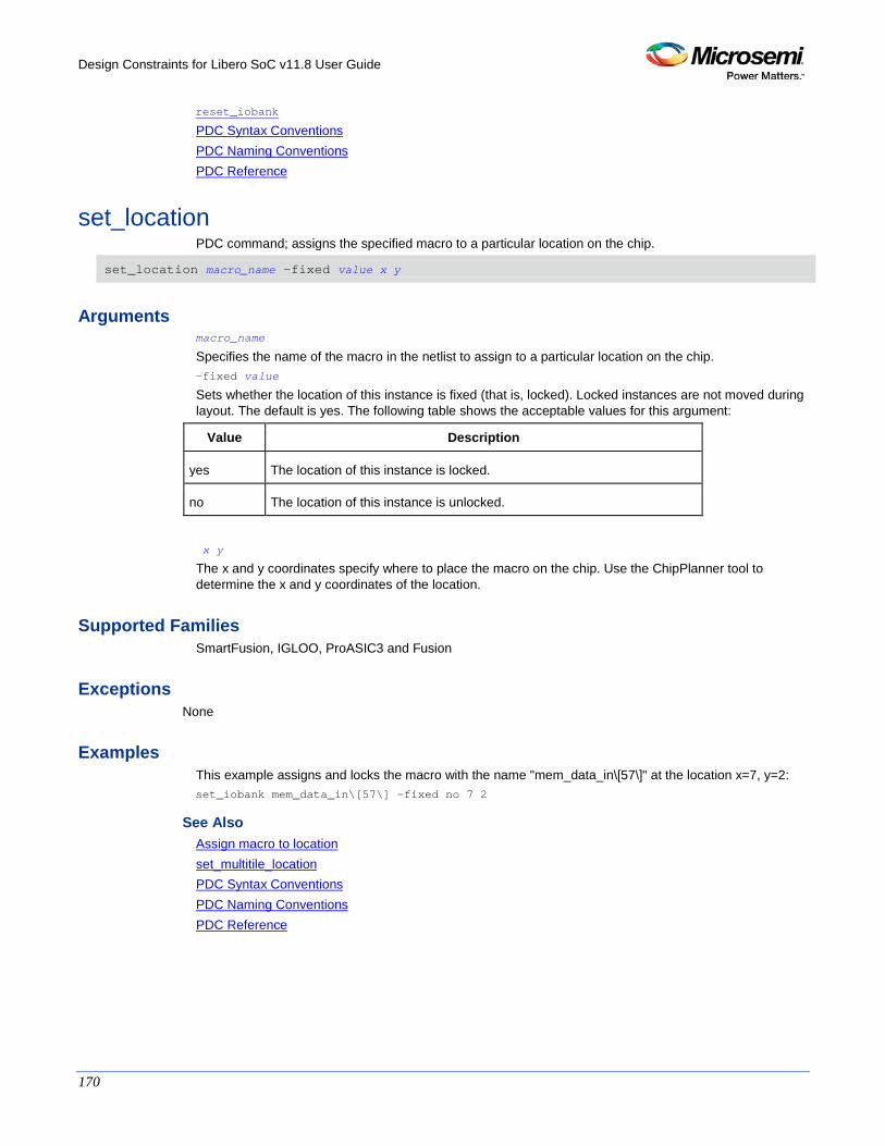
Design Constraints for Libero SoC v11.8 User Guide
170
reset_iobank
PDC Syntax Conventions PDC Naming Conventions PDC Reference
set_location PDC command; assigns the specified macro to a particular location on the chip.
set_location macro_name -fixed value x y
Arguments macro_name
Specifies the name of the macro in the netlist to assign to a particular location on the chip. -fixed value
Sets whether the location of this instance is fixed (that is, locked). Locked instances are not moved during layout. The default is yes. The following table shows the acceptable values for this argument:
Value Description
yes The location of this instance is locked.
no The location of this instance is unlocked.
x y
The x and y coordinates specify where to place the macro on the chip. Use the ChipPlanner tool to determine the x and y coordinates of the location.
Supported Families SmartFusion, IGLOO, ProASIC3 and Fusion
Exceptions None
Examples This example assigns and locks the macro with the name "mem_data_in\[57\]" at the location x=7, y=2: set_iobank mem_data_in\[57\] -fixed no 7 2
See Also Assign macro to location set_multitile_location PDC Syntax Conventions PDC Naming Conventions PDC Reference
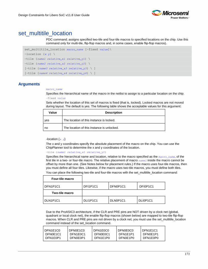
Design Constraints for Libero SoC v11.8 User Guide
171
set_multitile_location PDC command; assigns specified two-tile and four-tile macros to specified locations on the chip. Use this command only for multi-tile, flip-flop macros and, in some cases, enable flip-flop macros).
set_multitile_location macro_name [-fixed value]\
-location {x y} \
-tile {name1 relative_x1 relative_y1} \
-tile {name2 relative_x2 relative_y2} \
[-tile {name3 relative_x3 relative_y3} \ ]
[-tile {name4 relative_x4 relative_y4} \ ]
Arguments macro_name
Specifies the hierarchical name of the macro in the netlist to assign to a particular location on the chip. -fixed value
Sets whether the location of this set of macros is fixed (that is, locked). Locked macros are not moved during layout. The default is yes. The following table shows the acceptable values for this argument:
Value Description
yes The location of this instance is locked.
no The location of this instance is unlocked.
-location {x y} The x and y coordinates specify the absolute placement of the macro on the chip. You can use the ChipPlanner tool to determine the x and y coordinates of the location. -tile {name1 relative_x1 relative_y1}
Specifies the hierarchical name and location, relative to the macro specified as the macro_name, of the first tile in a two- or four-tile macro. The relative placement of macro name1 inside the macro cannot be offset by more than one. (See Notes below for placement rules.) If the macro uses four-tile macros, then you must define all four tiles. Likewise, if the macro uses two-tile macros, you must define both tiles. You can place the following two-tile and four-tile macros with the set_multitile_location command:
Four-tile macro
DFN1P1C1 DFI1P1C1 DFN0P1C1 DFI0P1C1
Two-tile macro
DLN1P1C1 DLI1P1C1 DLN0P1C1 DLI0P1C1
Due to the ProASIC3 architecture, if the CLR and PRE pins are NOT driven by a clock net (global, quadrant or local clock net), the enable flip-flop macros (shown below) are mapped to two-tile flip-flop macros. When CLR and PRE pins are not driven by a clock net, you must use the set_multitile_location command instead of the set_location command.
DFN1E1C0 DFN0E1C1 DFN1E0P1
DFN0E1C0 DFN1E0C1 DFN0E0P1
DFN1E0C0 DFN0E0C1 DFN1E1P0
DFN0E0C0 DFN1E1P1 DFN0E1P0
DFN1E1C1 DFN0E1P1 DFN1E0P0
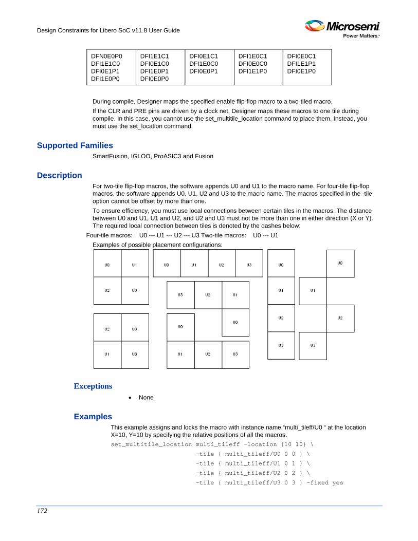
Design Constraints for Libero SoC v11.8 User Guide
172
DFN0E0P0 DFI1E1C0 DFI0E1P1 DFI1E0P0
DFI1E1C1 DFI0E1C0 DFI1E0P1 DFI0E0P0
DFI0E1C1 DFI1E0C0 DFI0E0P1
DFI1E0C1 DFI0E0C0 DFI1E1P0
DFI0E0C1 DFI1E1P1 DFI0E1P0
During compile, Designer maps the specified enable flip-flop macro to a two-tiled macro. If the CLR and PRE pins are driven by a clock net, Designer maps these macros to one tile during compile. In this case, you cannot use the set_multitile_location command to place them. Instead, you must use the set_location command.
Supported Families SmartFusion, IGLOO, ProASIC3 and Fusion
Description For two-tile flip-flop macros, the software appends U0 and U1 to the macro name. For four-tile flip-flop macros, the software appends U0, U1, U2 and U3 to the macro name. The macros specified in the -tile option cannot be offset by more than one. To ensure efficiency, you must use local connections between certain tiles in the macros. The distance between U0 and U1, U1 and U2, and U2 and U3 must not be more than one in either direction (X or Y). The required local connection between tiles is denoted by the dashes below:
Four-tile macros: U0 --- U1 --- U2 --- U3 Two-tile macros: U0 --- U1 Examples of possible placement configurations:
Exceptions • None
Examples This example assigns and locks the macro with instance name “multi_tileff/U0 “ at the location X=10, Y=10 by specifying the relative positions of all the macros. set_multitile_location multi_tileff -location {10 10} \
-tile { multi_tileff/U0 0 0 } \
-tile { multi_tileff/U1 0 1 } \
-tile { multi_tileff/U2 0 2 } \
-tile { multi_tileff/U3 0 3 } -fixed yes
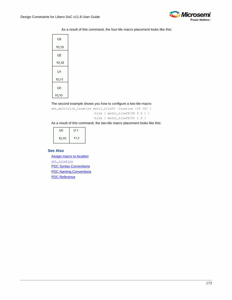
Design Constraints for Libero SoC v11.8 User Guide
173
As a result of this command, the four-tile macro placement looks like this:
The second example shows you how to configure a two-tile macro: set_multitile_location multi_tileff -location {10 10} \
-tile { multi_tileff/U0 0 0 } \
-tile { multi_tileff/U1 1 0 }
As a result of this command, the two-tile macro placement looks like this:
See Also Assign macro to location set_location
PDC Syntax Conventions PDC Naming Conventions PDC Reference
Design Constraints for Libero SoC v11.8 User Guide
174
set_net_critical PDC command; sets the net criticality, which influences place-and-route in favor of performance.
set_net_criticalcriticality_number [ hier_net_name]+
Arguments criticality_number
Sets the criticality level from 1 to 10, with 1 being the least critical and 10 being the most critical. The default is 5. Criticality numbers are used in timing-driven place and route. hier_net_name
Specifies the net name, which can be an AFL (Flattened Netlist) net name or a net regular expression using wildcard characters. You must specify at least one net name. You can use the following wildcard characters in names:
Wildcard What It Does
\ Interprets the next character as a non-special character
? Matches any single character
* Matches any string
[] Matches any single character among those listed between brackets (that is, [A-Z] matches any single character in the A-to-Z range)
Note: This command must have at least two parameters.
Supported Families SmartFusion, IGLOO, ProASIC3 and Fusion
Description Increasing a net’s criticality forces place-and-route to keep instances connected to the specified net as close as possible at the cost of other (less critical) nets.
Exceptions • The net names are AFL names, which means they must be visible in SmartTime and ChipPlanner.
Examples This example sets the criticality level to 9 for all addr nets: set_net_critical 9 addr*
See Also Set Net's Criticality reset_net_critical
PDC Syntax Conventions PDC Naming Conventions PDC Reference
Design Constraints for Libero SoC v11.8 User Guide
175
set_port_block PDC command; sets properties on a port in the block flow. This PDC command applies to only one I/O.
set_port_block -name portName -remove_ios value -add_interface value]
Arguments -name portName
Specify the name of the port. -remove_ios value
Sets whether or not to remove I/Os connected to the specified port from the netlist. The following table shows the acceptable values for this argument:
Value Description
yes Remove I/Os connected to the specified port from the netlist.
no Do not remove I/Os connected to the specified port from the netlist.
-add_interface value
Adds an interface macro each time the fanout of the net connected to the port is greater than the value specified. The value must be a positive integer.
Supported Families SmartFusion2, IGLOO2, RTG4, SmartFusion, IGLOO, ProASIC3, Fusion
Exceptions • You must import this PDC command as a source file, not as an auxiliary file. • TRIBUFF and BIBUF macros cannot be removed even if you specify "-remove_ios yes". • You must enable the block flow before calling this command. To enable the block flow, either select
the "Enable block mode" option in the Setup Design dialog box, or use the -block argument in the new_design Tcl command to enable block mode.
Examples This example removes any I/Os connected to portA, excluding TRIBUFF and BIBUF I/Os: set_port_block -name portA -remove_ios yes
See Also new_design
PDC Reference
Design Constraints for Libero SoC v11.8 User Guide
176
set_preserve PDC command; sets a preserve property on instances before compile, so compile will preserve these instances and not combine them.
set_preserve hier_inst_name
Arguments hier_inst_name
Specifies the full hierarchical name of the macro in the netlist to preserve.
Supported Families SmartFusion2, IGLOO2, RTG4, SmartFusion, IGLOO, ProASIC3, Fusion
Exceptions • This command is not supported in post compiled designs. If importing a PDC file that includes this
command, you must import it as a source file.
Examples In some cases, you may want to preserve some instances for timing purposes. For example, you may want registers to be combined with input of a bibuf and keep the output as it is. If the outbuf of a bi-directional signal test[1] needs to be preserved while inbuf is required to combine with the registers, use the following PDC commands: set_io test\[1\] -REGISTER yes
set_preserve test\[31\]
If any internal instance is required to be preserved, use the set_preserve command as shown in the following example: set_preserve top/inst1 top/inst2
See Also PDC Syntax Conventions PDC Naming Conventions I/O Register Combining PDC Reference
Design Constraints for Libero SoC v11.8 User Guide
177
unassign_global_clock PDC command; demotes clock nets to regular nets. The unassign_global_clock command is not supported in auxiliary PDC files.
unassign_global_clock -net netname
Arguments -net netname
Specifies the name of the clock net to demote to a regular net.
Supported Families SmartFusion, IGLOO, ProASIC3 and Fusion
Exceptions • You cannot assign “essential” clock nets to regular nets. Clock nets that are driven by the following
macros are “essential” global nets: CLKDLY, PLL, and CLKBIBUF.
Examples unassign_global_clock -net globalReset
See Also assign_global_clock
PDC Syntax Conventions PDC Naming Conventions PDC Reference
Design Constraints for Libero SoC v11.8 User Guide
178
unassign_local_clock PDC command; unassigns the specified net from a LocalClock region.
unassign_local_clock -net netname
Arguments -net netname
Specifies the name of the net to unassign.
Supported Families SmartFusion, IGLOO, ProASIC3 and Fusion
Exceptions This command is not supported in auxiliary PDC files. If importing a PDC file that includes this command, you must import it as a source file.
Examples This example unassigns the net named reset_n from the local clock region: unassign_local_clock -net reset_n
See Also assign_local_clock (IGLOO, Fusion, and ProASIC3)
PDC Syntax Conventions PDC Naming Conventions PDC Reference
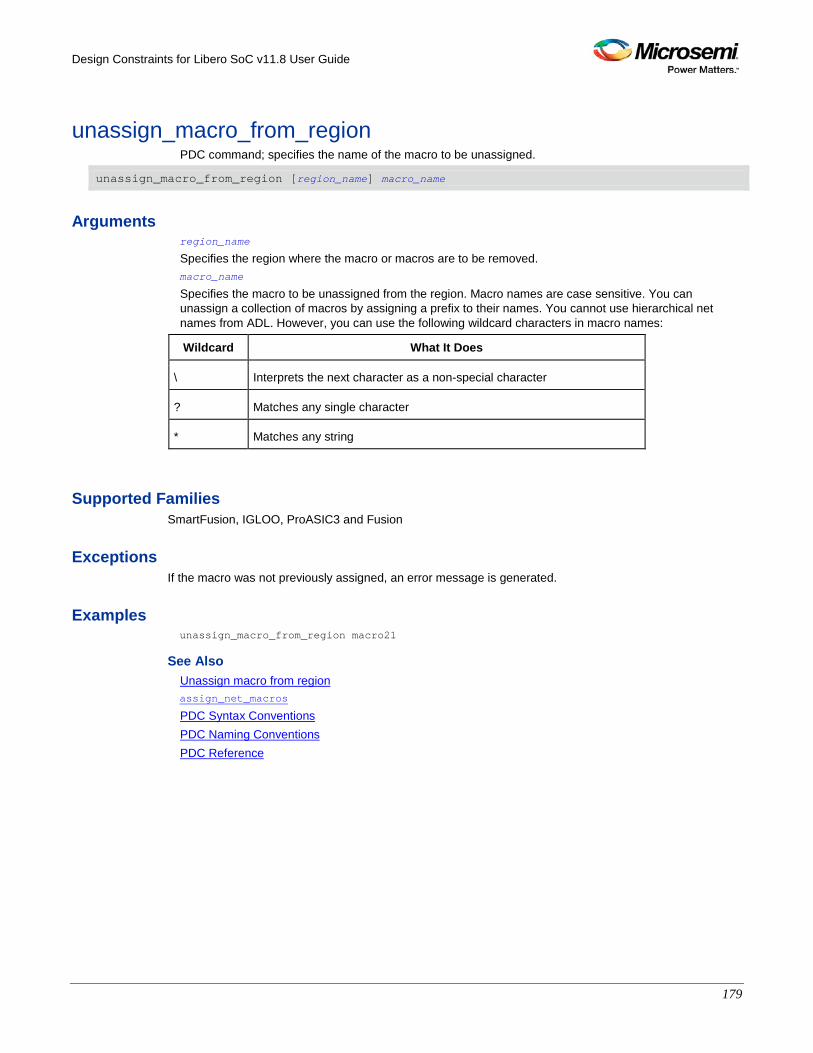
Design Constraints for Libero SoC v11.8 User Guide
179
unassign_macro_from_region PDC command; specifies the name of the macro to be unassigned.
unassign_macro_from_region [region_name] macro_name
Arguments region_name
Specifies the region where the macro or macros are to be removed. macro_name
Specifies the macro to be unassigned from the region. Macro names are case sensitive. You can unassign a collection of macros by assigning a prefix to their names. You cannot use hierarchical net names from ADL. However, you can use the following wildcard characters in macro names:
Wildcard What It Does
\ Interprets the next character as a non-special character
? Matches any single character
* Matches any string
Supported Families SmartFusion, IGLOO, ProASIC3 and Fusion
Exceptions If the macro was not previously assigned, an error message is generated.
Examples unassign_macro_from_region macro21
See Also Unassign macro from region assign_net_macros
PDC Syntax Conventions PDC Naming Conventions PDC Reference
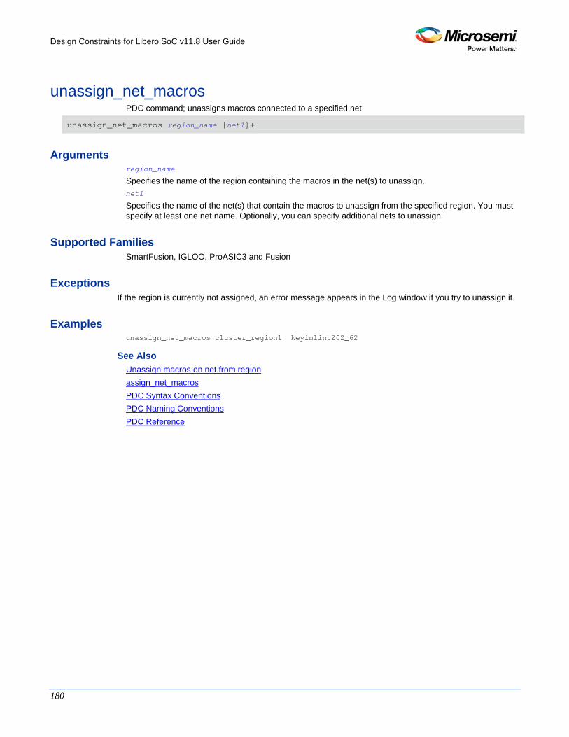
Design Constraints for Libero SoC v11.8 User Guide
180
unassign_net_macros PDC command; unassigns macros connected to a specified net.
unassign_net_macros region_name [net1]+
Arguments region_name
Specifies the name of the region containing the macros in the net(s) to unassign. net1
Specifies the name of the net(s) that contain the macros to unassign from the specified region. You must specify at least one net name. Optionally, you can specify additional nets to unassign.
Supported Families SmartFusion, IGLOO, ProASIC3 and Fusion
Exceptions If the region is currently not assigned, an error message appears in the Log window if you try to unassign it.
Examples unassign_net_macros cluster_region1 keyin1intZ0Z_62
See Also Unassign macros on net from region assign_net_macros PDC Syntax Conventions PDC Naming Conventions PDC Reference
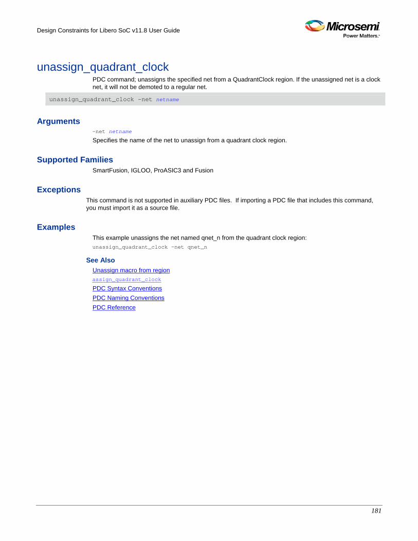
Design Constraints for Libero SoC v11.8 User Guide
181
unassign_quadrant_clock PDC command; unassigns the specified net from a QuadrantClock region. If the unassigned net is a clock net, it will not be demoted to a regular net.
unassign_quadrant_clock -net netname
Arguments -net netname
Specifies the name of the net to unassign from a quadrant clock region.
Supported Families SmartFusion, IGLOO, ProASIC3 and Fusion
Exceptions This command is not supported in auxiliary PDC files. If importing a PDC file that includes this command, you must import it as a source file.
Examples This example unassigns the net named qnet_n from the quadrant clock region: unassign_quadrant_clock -net qnet_n
See Also Unassign macro from region assign_quadrant_clock
PDC Syntax Conventions PDC Naming Conventions PDC Reference
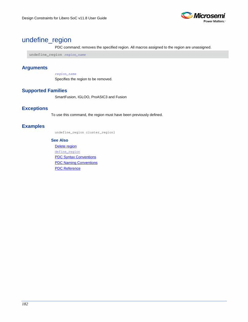
Design Constraints for Libero SoC v11.8 User Guide
182
undefine_region PDC command; removes the specified region. All macros assigned to the region are unassigned.
undefine_region region_name
Arguments region_name
Specifies the region to be removed.
Supported Families SmartFusion, IGLOO, ProASIC3 and Fusion
Exceptions To use this command, the region must have been previously defined.
Examples undefine_region cluster_region1
See Also Delete region define_region
PDC Syntax Conventions PDC Naming Conventions PDC Reference

Design Constraints for Libero SoC v11.8 User Guide
183
unreserve PDC command; resets the named pins in the current device, so they are no longer reserved. You can then use these pins in your design.
unreserve -pinname "list of package pins"
Arguments -pinname "list of package pins"
Specifies the package pin name(s) to unreserve.
Supported Families SmartFusion, IGLOO, ProASIC3 and Fusion
Exceptions None
Examples unreserve -pinname "F2"
unreserve -pinname "F2 B4 B3"
unreserve -pinname "124 63"
See Also reserve
PDC Syntax Conventions PDC Naming Conventions PDC Reference
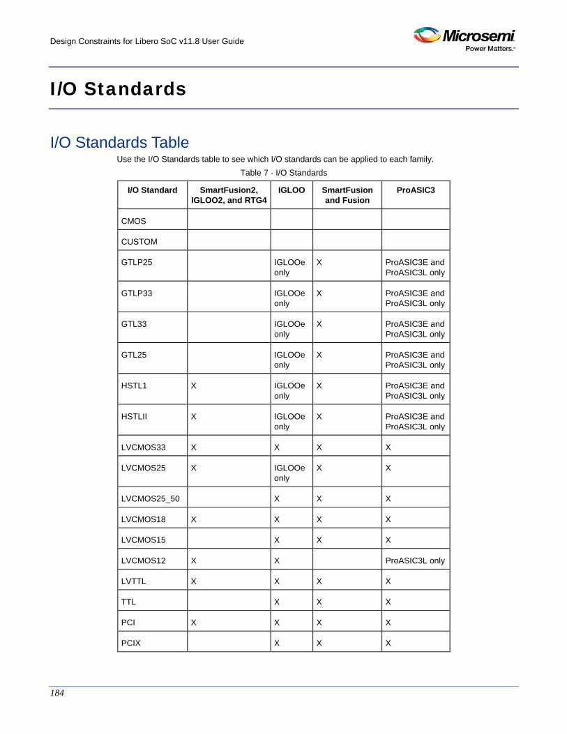
Design Constraints for Libero SoC v11.8 User Guide
184
I/O Standards
I/O Standards Table Use the I/O Standards table to see which I/O standards can be applied to each family.
Table 7 · I/O Standards
I/O Standard SmartFusion2, IGLOO2, and RTG4
IGLOO SmartFusion and Fusion
ProASIC3
CMOS
CUSTOM
GTLP25 IGLOOe only
X ProASIC3E and ProASIC3L only
GTLP33 IGLOOe only
X ProASIC3E and ProASIC3L only
GTL33 IGLOOe only
X ProASIC3E and ProASIC3L only
GTL25 IGLOOe only
X ProASIC3E and ProASIC3L only
HSTL1 X IGLOOe only
X ProASIC3E and ProASIC3L only
HSTLII X IGLOOe only
X ProASIC3E and ProASIC3L only
LVCMOS33 X X X X
LVCMOS25 X IGLOOe only
X X
LVCMOS25_50 X X X
LVCMOS18 X X X X
LVCMOS15 X X X
LVCMOS12 X X ProASIC3L only
LVTTL X X X X
TTL X X X
PCI X X X X
PCIX X X X
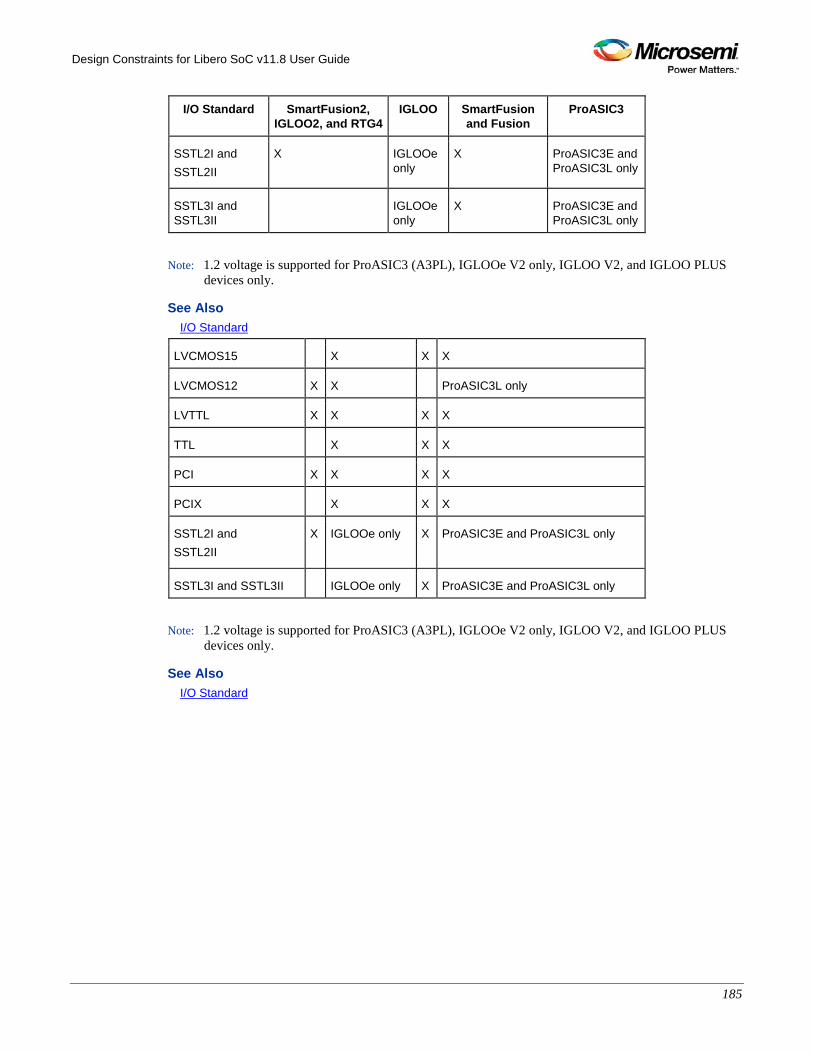
Design Constraints for Libero SoC v11.8 User Guide
185
I/O Standard SmartFusion2, IGLOO2, and RTG4
IGLOO SmartFusion and Fusion
ProASIC3
SSTL2I and SSTL2II
X IGLOOe only
X ProASIC3E and ProASIC3L only
SSTL3I and SSTL3II
IGLOOe only
X ProASIC3E and ProASIC3L only
Note: 1.2 voltage is supported for ProASIC3 (A3PL), IGLOOe V2 only, IGLOO V2, and IGLOO PLUS
devices only.
See Also I/O Standard
LVCMOS15 X X X
LVCMOS12 X X ProASIC3L only
LVTTL X X X X
TTL X X X
PCI X X X X
PCIX X X X
SSTL2I and SSTL2II
X IGLOOe only X ProASIC3E and ProASIC3L only
SSTL3I and SSTL3II IGLOOe only X ProASIC3E and ProASIC3L only
Note: 1.2 voltage is supported for ProASIC3 (A3PL), IGLOOe V2 only, IGLOO V2, and IGLOO PLUS
devices only.
See Also I/O Standard