Embed Size (px)
Citation preview

Rohouma, Wesam M.M. (2013) Design control and implementation of a four-leg matrix converter for ground power supply application. PhD thesis, University of Nottingham.
Access from the University of Nottingham repository: http://eprints.nottingham.ac.uk/13260/1/Wesam_Rohouma_Thesis.pdf
Copyright and reuse:
The Nottingham ePrints service makes this work by researchers of the University of Nottingham available open access under the following conditions.
This article is made available under the University of Nottingham End User licence and may be reused according to the conditions of the licence. For more details see: http://eprints.nottingham.ac.uk/end_user_agreement.pdf
For more information, please contact [email protected]
Design control and implementation of a
four-leg Matrix Converter for ground
power supply application
Wesam M. M Rohouma
Thesis submitted to the University of Nottingham
for the degree of Doctor of Philosophy
Feb, 2013
i
Abstract:
The technology of direct AC/AC power conversion (Matrix Converters) is gaining
increasing interest in the scientific community, particularly for aerospace
applications.
The aim of this research project is to investigate the use of direct AC/AC three phase
four-leg Matrix Converter as ground power unit to supply aircraft with power during
stopover or maintenance in airports. The converter fourth leg is used to provide a
path for the zero sequence components when feeding unbalanced or non-linear loads.
A high bandwidth controller is required to regulate the output voltage of Matrix
Converter with a 400Hz output frequency. However, the controller bandwidth is
limited due to the reduced ratio between the converter switching frequency and the
fundamental frequency. In this case undesirable, periodic errors and distortion will
exist in the output voltage above all in the presence of a non-linear or unbalanced
load.
Digital repetitive control system is proposed to regulate the output voltage of a four-
leg Matrix Converter in an ABC reference frame. The proposed control structure
introduces a high gain at the fundamental and its integer multiple frequencies. Using
the proposed repetitive controller will reduce the tracking error between the output
and the reference voltage, as well as increasing the stability of the converter under
balanced and unbalanced load conditions.
Simulation studies using SABER and MATLAB software packages show that the
proposed controller is able to regulate the output voltage during balanced and
unbalanced load conditions and during the presence of non-linear load. In order to
validate the effectiveness of the proposed controller, an experimental prototype of a
7.5KW has been implemented in PEMC laboratory using DSP/FPGA platform to
control the converter prototype. The steady state and the dynamic performance of the
proposed control strategy are investigated in details, and extensive experimental tests
have showed that the proposed controller was able to offer high tracking accuracy,
fast transient response and able to regulate the output voltage during balanced,
unbalanced and non-linear loading.

ii
Acknowledgement
All praise and thanks to Allah the Almighty, for giving me strength and ability to
complete this study.
I express my profound gratitude and sincere thanks to my supervisors Prof Patrick
Wheeler and Dr Pericle Zanchatta for their valuable suggestions and consistent
encouragement through the whole course of my research. I would like to thank all the
staff of the PEMC group at the University of Nottingham and all of the technicians of
the ground floor workshop, for providing the necessary help, to carry out this
research. All of you, who have contributed, all of you who encouraged me and
supported these pages, thank you.
Also, my deepest gratitude and thanks always go to my beloved parents, brothers,
sisters, all of my relatives and friends who have always been enriching my life with
their continuous support and love.
And last but not least, I would like to express my deepest gratitude, love and respect
to my wife and children. Without their support and patience, there would never be
any chance for this work to happen.
Nottingham, 2012
Wesam Rohouma

iii
Table of Contents
Abstract: .................................................................................................................... i
Acknowledgement .................................................................................................... ii
Table of Contents .................................................................................................... iii
List of symbols ...................................................................................................... viii
List of figures .......................................................................................................... ix
List of tables ......................................................................................................... xvii
Chapter 1 Introduction: ................................................................................................ 1
1.1 Introduction ........................................................................................................ 1
1.2 Power supply aircraft standards ......................................................................... 3
1.3 Matrix Converters: ............................................................................................. 5
1.3.1 Matrix Converter control ............................................................................. 6
1.4 Repetitive control ............................................................................................... 6
1.5 Objectives ........................................................................................................... 7
1.6 Thesis outlines .................................................................................................... 7
Chapter 2 Fundamentals of Matrix Converters ............................................................ 9
2.1 Introduction: ....................................................................................................... 9
2.2 Matrix Converter structure ............................................................................... 10
2.2.1 Input filter .................................................................................................. 10
2.2.2 Output filter................................................................................................ 12
2.2.3 Bidirectional switches ................................................................................ 13
iv
2.3 Matrix Converter Current Commutation .......................................................... 15
2.3.1 Simple Commutation Methods .................................................................. 15
2.3.2 Soft switching techniques .......................................................................... 16
2.3.3 Advanced commutation methods............................................................... 16
2.3.4 Output current direction based commutation method. ............................... 16
2.4 Matrix Converter modulation strategies ........................................................... 18
2.4.1 Space Vector Modulation for 3x3 Matrix Converter ................................. 19
2.4.2 Space Vector Modulation for 3x4 Matrix Converter ................................. 23
2.4.3 Principles of the Venturini modulation method ......................................... 30
2.4.4 Switching Sequence of the Four-Leg Matrix Converter ............................ 34
2.5 Summary .......................................................................................................... 37
Chapter 3 Control design for the four-leg Matrix Converter power supply .............. 38
3.1 Introduction ...................................................................................................... 38
3.2 Modeling and control of four-leg Matrix Converter system ............................ 39
3.2.1 Averaged model of the four-leg Matrix Converter .................................... 39
3.2.2 GPU based four-leg Matrix Converter control in ABC reference frame ... 40
3.2.3 Linear second order control design example for the four-leg Matrix
Converter ............................................................................................................ 42
3.3 Repetitive Control ............................................................................................ 46
3.3.1 Repetitive control classification................................................................. 47
3.3.2 Fundamentals of repetitive control ............................................................ 48

v
3.3.3 Plug-in Discrete Repetitive Controller ...................................................... 50
3.3.4 Stability Analysis ....................................................................................... 52
3.3.5 Design of the robustness filter Q(z) ........................................................... 55
3.3.6 Time advance unit (ZL) design .................................................................. 58
3.3.7 Design example of four-leg Matrix Converter using second order linear
controller and plug-in repetitive controller ......................................................... 60
3.4 Summary .......................................................................................................... 63
Chapter 4 Power converter simulation ....................................................................... 64
4.1 Introduction ...................................................................................................... 64
4.2 Power converter modeling and simulation ....................................................... 65
4.3 GPU simulation ................................................................................................ 66
5.1.1. Saber simulation of four-leg Matrix Converter ........................................ 67
4.3.1 Simulation flowchart.................................................................................. 69
4.3.2 System parameters ..................................................................................... 71
4.3.3 Matrix Converter operation under balanced load ...................................... 71
4.3.4 Unbalanced load conditions ....................................................................... 77
4.3.5 Non Linear Load ........................................................................................ 85
4.3.6 Load disconnection and connection ........................................................... 92
4.4 Switching frequency effect on power converter performance ......................... 95
4.4.1 Simulation results using 8kHz switching frequency.................................. 96
4.4.2 Simulation results using 12.8kHz switching frequency........................... 100

vi
4.4.3 Simulation results using 25.6kHz switching frequency........................... 104
4.5 Summery ........................................................................................................ 108
Chapter 5 Hardware Implementation ....................................................................... 110
5.1 Introduction .................................................................................................... 110
5.2 Experimental rig ............................................................................................. 111
5.3 Input filter ....................................................................................................... 112
5.4 Power modules (Bidirectional switches) ........................................................ 114
5.5 Gate drive circuit ............................................................................................ 115
5.6 Current direction circuit ................................................................................. 117
5.7 Voltage clamp circuit ..................................................................................... 119
5.8 Measurement circuit ....................................................................................... 121
5.9 Output filter .................................................................................................... 123
5.10 Control platform ........................................................................................... 125
5.10.1 Digital signal processor DSP ................................................................. 126
5.10.2 Field Programmable Gate Array (FPGA) board .................................... 126
5.10.3 DSP software overview ......................................................................... 128
5.11 Summery ...................................................................................................... 131
Chapter 6 Experimental Results ............................................................................... 132
6.1 Introduction .................................................................................................... 132
6.2 System parameters .......................................................................................... 133
6.3 Matrix Converter operation for a balanced load............................................. 134

vii
6.4 Unbalanced load conditions ........................................................................... 139
6.5 Non Linear Load ............................................................................................ 146
6.6 Load connection and disconnection ............................................................... 153
6.7 Summery ........................................................................................................ 155
Chapter 7 Conclusion ............................................................................................... 158
7.1 Conclusion ...................................................................................................... 158
7.2 Future work .................................................................................................... 161
References ............................................................................................................ 162
Appendices ............................................................................................................... 171
Appendix A : Published Papers ............................................................................ 171
Under revision jpurnal paper: ............................................................................... 171
Appendix B :Duty cycles to space vector transformation .................................... 172

viii
List of symbols
Rs Input damping resistor.
Ls Input filter inductance.
Cs Input filter capacitance.
Lo Output filter inductance.
Co Output filter capacitance.
Va,Vb,Vc,Vn Output phase voltages.
VA, VB, VC Input phase voltages.
RL Value of load resistance.
LL Value of load inductance.
Kv Sector number that contains the output voltage vector.
Ki Sector number that contains the input current vector.
Vim Peak input voltage.
q Voltage transfer ratio.
URC Repetitive control output.
Q(z) Low pass filter.
Z-N
Delay element
Z-L
Delay element.
Gc(z) Controller transfer function.
Gp(z) Plant transfer function.

ix
List of figures
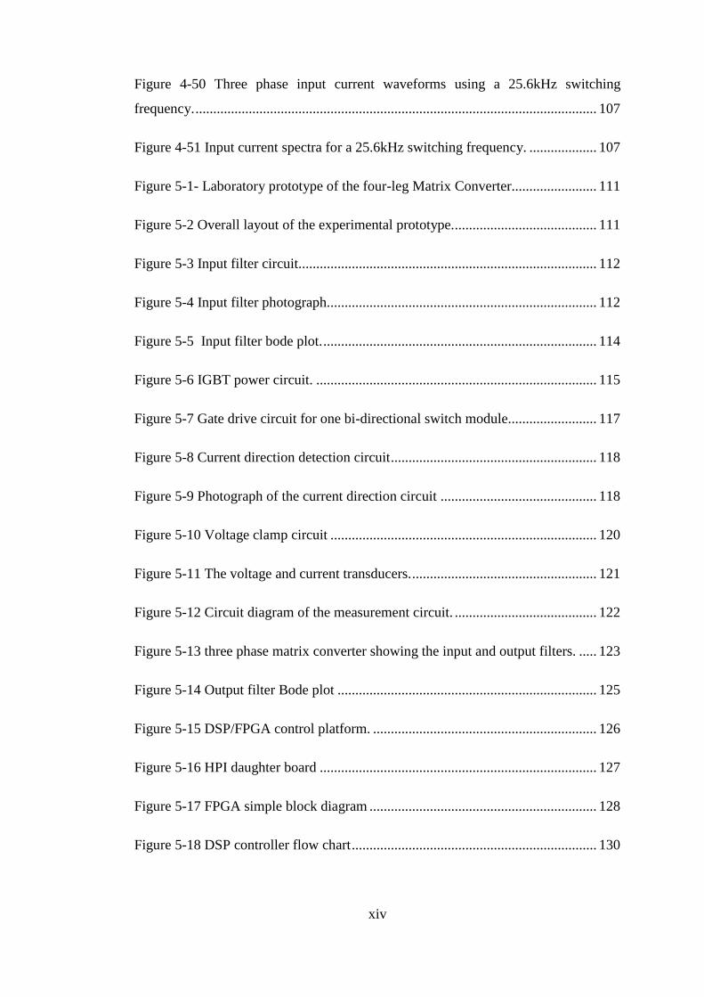
Figure 1-1 GPU possible topologies. ........................................................................... 2
Figure 1-2 Envelope of normal 400 Hz and variable frequency AC voltage transient.3
Figure 1-3 Matrix Converter with ABC reference control........................................... 4
Figure 2-1 Four-leg Matrix Converter system ........................................................... 10
Figure 2-2 Input filter circuit...................................................................................... 11
Figure 2-3 Input filter Single phase equivalent circuit............................................... 12
Figure 2-4 Three phase matrix converter circuit. ....................................................... 13
Figure 2-5 Output filter single phase equivalent circuit. ............................................ 13
Figure 2-6 Bidirectional switches configuration ........................................................ 14
Figure 2-7 Current direction based commutation. ..................................................... 17
Figure 2-8 Four step current commutation................................................................. 17
Figure 2-9 Four step current commutation................................................................. 18
Figure 2-10 SVM Vectors for a Balanced 3-Phase .................................................... 20
Figure 2-11 Output voltage and input current space vectors ..................................... 20
Figure 2-12 Input voltage space. ................................................................................ 24
Figure 2-13 α,β,γ space vector for four-leg Matrix Converter. .................................. 28
Figure 2-14 (A) Three dimensional view of the vectors in α,β plane, (B) in 3
dimensional plan. ....................................................................................................... 29
Figure 2-15 Target output and input voltage.............................................................. 32
Figure 2-16 Target output voltage using optimized Venturini modulation. .............. 33

x
Figure 2-17 Switching sequence for output phase a. ................................................. 35
Figure 2-18 Output phase voltage (a) using basic Venturini modulation. ................. 35
Figure 2-19 Output line voltage Vab using basic Venturini modulation. ................... 36
Figure 2-20 Switching sequence according to input voltage vector position. ........... 37
Figure 2-21 Line to line output voltage using cyclic Venturini ................................. 37
Figure 3-1 Simplified single phase close loop system of the converter. .................... 40
Figure 3-2 Root locus of Gp(z)*Gc(z) ....................................................................... 44
Figure 3-3 Bode plot of the Gp(z) and Gp(z)*Gc(z).................................................. 45
Figure 3-4 Output voltage response of the converter using second order linear
controller. ................................................................................................................... 45
Figure 3-5 Direct structure repetitive control............................................................. 47
Figure 3-6 Parallel structure repetitive control. ......................................................... 47
Figure 3-7 plug-in type repetitive control. ................................................................. 48
Figure 3-8 Periodic signal generator .......................................................................... 49
Figure 3-9 Bode plot of periodic generator. ............................................................... 49
Figure 3-10 Block diagram of the overall system. ..................................................... 50
Figure 3-11 Different repetitive controller structure[76]. .......................................... 51
Figure 3-12 Equivalent system block diagram of equation 3-16 ............................... 52
Figure 3-13 Pole zero map of the system in Figure 3-8 ............................................. 53
Figure 3-14 Negative feedback system ...................................................................... 53
Figure 3-15 The Nyquist diagram of S(z). ................................................................. 55

xi
Figure 3-16 Bode plot of Q(z). ................................................................................... 56
Figure 3-17 Bode plot of Grc(z) using Q(z) as a constant and as a low pass filter.... 57
Figure 3-18 Pole zero map of Grc(z) using Q(z) as a low pass filter, (z+2+z-1
)/4..... 57
Figure 3-19 Bode plot of Gc(z) Gp(z)........................................................................ 59
Figure 3-20 Reference and output voltage using second order linear controller only.
.................................................................................................................................... 59
Figure 3-21 Proposed plug-in repetitive controller. ................................................... 61
Figure 3-22 Output voltage compared with the reference using plug-in repetitive
controller. ................................................................................................................... 62
Figure 3-23 proposed repetitive controller. ................................................................ 62
Figure 4-1 GPU structure ........................................................................................... 65
Figure 4-2 Modelling levels. ...................................................................................... 66
Figure 4-3 Matrix Converter system. ......................................................................... 68
Figure 4-4 Modulation and control simulation flow chart. ........................................ 70
Figure 4-5 Phase A unfiltered output voltage. ........................................................... 72
Figure 4-6 Three-phase output voltage for a balanced load. ...................................... 72
Figure 4-7 Filtered output voltage spectra for a balanced load .................................. 73
Figure 4-8 R.M.S output voltage for a balanced load phase A. ................................. 73
Figure 4-9 Output voltage tracking for a balanced load phase A. ............................. 74
Figure 4-10 Three phase output currents for a balanced load. ................................... 75
Figure 4-11 Unfiltered input current in phase A. ....................................................... 75
Figure 4-12 Filtered three phase input currents for a balanced load. ......................... 76

xii
Figure 4-13 Filtered input current spectra of phase A, for a balanced load. .............. 76
Figure 4-14 The three phase output voltages for an unbalanced load. ...................... 77
Figure 4-15 FFT of output phase voltage A for an unbalanced load. ........................ 78
Figure 4-16 FFT of output phase voltage B for an unbalanced load. ........................ 78
Figure 4-17 FFT of output phase voltage C for an unbalanced load. ........................ 79
Figure 4-18 Output voltage tracking of phase (a) for an unbalanced load. ................ 80
Figure 4-19 Output voltage tracking of phase (b) for an unbalanced load. ............... 81
Figure 4-20 Output voltage tracking of phase (c) for an unbalanced load. ................ 82
Figure 4-21 Output currents for the unbalance load condition. ................................. 83
Figure 4-22 Three phase input currents for an unbalanced load. ............................... 84
Figure 4-23 Input current spectra of phase A, for an unbalanced load ...................... 84
Figure 4-24 Three phase non-linear load circuit. ....................................................... 85
Figure 4-25 Non-linear load current .......................................................................... 86
Figure 4-26 Three phase output voltages for a non-linear load ................................. 86
Figure 4-27 Output voltage spectrum with non-linear load (phase A). ..................... 87
Figure 4-28 Output voltage spectrum with non-linear load (phase B)....................... 87
Figure 4-29 Output voltage spectrum with non-linear load (phase C)....................... 88
Figure 4-30 Output voltage tracking for a Non-linear load. ...................................... 89
Figure 4-31 Three phase output currents with non-linear load. ................................. 90
Figure 4-32 Three phase input currents with non-linear load. ................................... 91
Figure 4-33 Input current spectra of phase A, for a non-linear load. ......................... 91
xiii
Figure 4-34 Output voltage response due to a three phase load disconnection ......... 93
Figure 4-35 Output voltage response due to a three phase load connection .............. 94
Figure 4-36 The effect of increasing the switching frequency on output voltage’s
quality. ........................................................................................................................ 95
Figure 4-37 Three phase output voltage waveforms using an 8kHz switching
frequency. ................................................................................................................... 97
Figure 4-38 Output voltage spectra using an 8kHz switching frequency. ................. 97
Figure 4-39 Output voltage tracking of phase A for an 8kHz switching frequency. . 98
Figure 4-40 Three phase input current waveforms using an 8kHz switching
frequency. ................................................................................................................... 99
Figure 4-41 Filtered input current spectra for an 8kHz switching frequency. ........... 99
Figure 4-42 Three phase output voltage waveforms using a 12.8kHz switching
frequency. ................................................................................................................. 100
Figure 4-43 Output voltage spectra using a 12.8 kHz switching frequency ............ 101
Figure 4-44 Output voltage tracking of phase A for a 12.8kHz switching frequency.
.................................................................................................................................. 102
Figure 4-45 Three phase input current waveforms using a 12.8kHz switching
frequency. ................................................................................................................. 103
Figure 4-46 Input current spectra for a 12.8kHz switching frequency. ................... 103
Figure 4-47 Three phase output voltage waveforms using a 25.6kHz switching
frequency. ................................................................................................................. 104
Figure 4-48 Output voltage spectra using a 25.6 kHz switching frequency ............ 105
Figure 4-49 Output voltage tracking of phase A for a 25.6kHz switching frequency.
.................................................................................................................................. 106
xiv
Figure 4-50 Three phase input current waveforms using a 25.6kHz switching
frequency. ................................................................................................................. 107
Figure 4-51 Input current spectra for a 25.6kHz switching frequency. ................... 107
Figure 5-1- Laboratory prototype of the four-leg Matrix Converter........................ 111
Figure 5-2 Overall layout of the experimental prototype......................................... 111
Figure 5-3 Input filter circuit.................................................................................... 112
Figure 5-4 Input filter photograph............................................................................ 112
Figure 5-5 Input filter bode plot. ............................................................................. 114
Figure 5-6 IGBT power circuit. ............................................................................... 115
Figure 5-7 Gate drive circuit for one bi-directional switch module......................... 117
Figure 5-8 Current direction detection circuit .......................................................... 118
Figure 5-9 Photograph of the current direction circuit ............................................ 118
Figure 5-10 Voltage clamp circuit ........................................................................... 120
Figure 5-11 The voltage and current transducers. .................................................... 121
Figure 5-12 Circuit diagram of the measurement circuit. ........................................ 122
Figure 5-13 three phase matrix converter showing the input and output filters. ..... 123
Figure 5-14 Output filter Bode plot ......................................................................... 125
Figure 5-15 DSP/FPGA control platform. ............................................................... 126
Figure 5-16 HPI daughter board .............................................................................. 127
Figure 5-17 FPGA simple block diagram ................................................................ 128
Figure 5-18 DSP controller flow chart ..................................................................... 130

xv
Figure 6-1 Experimental prototype of four-leg Matrix Converter. .......................... 133
Figure 6-2 Output phase to neutral voltage measured before the output filter ........ 134
Figure 6-3 Output voltage for a balanced load......................................................... 135
Figure 6-4 FFT of output phase a balanced load. .................................................... 135
Figure 6-5 R.M.S output voltage for a balanced load. ............................................. 136
Figure 6-6 Output voltage tracking for a balanced load. ......................................... 137
Figure 6-7 Output currents balanced load. Add captions ......................................... 138
Figure 6-8 Three phase input currents balanced load .............................................. 138
Figure 6-9 Input current spectra of phase A, for a balanced load condition. ........... 139
Figure 6-10 Three phase unbalanced load circuit. ................................................... 140
Figure 6-11 Three phase output voltages for an unbalanced load. .......................... 141
Figure 6-12 FFT of output phase (a) for an unbalanced load. ................................. 141
Figure 6-13 FFT of output phase b for an unbalanced load. .................................... 142
Figure 6-14 FFT of output phase c for an unbalanced load. .................................... 142
Figure 6-15 Output voltage tracking for an unbalanced load. ................................. 143
Figure 6-16 Output currents for an unbalance conditions. ....................................... 144
Figure 6-17 Three phase input currents for an unbalanced load. ............................. 145
Figure 6-18 Input current spectra of phase A, for unbalanced load condition. ........ 145
Figure 6-19 Three phase non-linear load circuit. ..................................................... 146
Figure 6-20 Three phase output voltages for a non-linear load ............................... 147
Figure 6-21 Output voltage spectrum with non-linear load (phase A). ................... 148

xvi
Figure 6-22 Output voltage spectrum with non-linear load (phase B)..................... 148
Figure 6-23 Output voltage spectrum with non-linear load (phase C)..................... 149
Figure 6-24 The output voltage tracking for a Non-linear load. .............................. 150
Figure 6-25 Three phase output currents with non-linear load. ............................... 151
Figure 6-26 Three phase input currents with non-linear load. ................................. 152
Figure 6-27 Input current spectra of phase A, for a non-linear load condition ........ 152
Figure 6-28 Output voltage response due to load connection. ................................. 154
Figure 6-29 Output voltage response due to load disconnection ............................. 155
Figure B1: Cyclic Venturini switching sequence where kv=1, ki=1, Tetrahedron=2.
……………………………………………………………………………...173

xvii
List of tables
Table 1-1 Military standards for aircraft electrical power systems [5]. ....................... 3
Table 2-1 Switching states of three phase Matrix Converter[57] . ............................ 21
Table 2-2 Selection of switching configuration according to output voltage and input
current sectors [13]. .................................................................................................... 22
Table 2-3 Rotating vector states for four-leg Matrix Converter. ............................... 26
Table 2-4 zero vectors and stationary states for four-leg Matrix Converter. ............. 27
Table 4-1 Summary of the simulation results for four-leg Matrix Converter system.
.................................................................................................................................. 108
Table 4-2 The effect of increasing the switching frequency on Matrix Converter
performance.............................................................................................................. 109
Table 6-1 Matrix Converter parameters. .................................................................. 133
Table 6-2 Summary of the simulation and experemintal results for four-leg Matrix
Converter system. ..................................................................................................... 157
Table B-2: Ki = 1 , Tetrahedron = 2. ...................................................................... 171
Table B-3: Ki = 1 , Tetrahedron = 3. ....................................................................... 171
Table B-4: Ki = 2 , Tetrahedron = 2. ....................................................................... 172
Table B-5: Ki = 2 , Tetrahedron = 3. ....................................................................... 172
Table B-6: Ki = 3 , Tetrahedron = 2. ....................................................................... 173
Table B-7: Ki = 3 , Tetrahedron = 3. ....................................................................... 173
Table B-8: Ki = 4 , Tetrahedron = 2. ...................................................................... 174
Table B-9: Ki = 4 , Tetrahedron = 3. ....................................................................... 174

xviii
Table B-10: Ki = 5 , Tetrahedron = 2. ..................................................................... 175
Table B-11: Ki = 5 , Tetrahedron = 3. ..................................................................... 175
Table B-12: Ki = 6 , Tetrahedron = 2. ..................................................................... 176
Table B-13: Ki = 6 , Tetrahedron = 3. .................................................................... 176
Chapter 1: Introduction
1
Chapter 1 Introduction:
1.1 Introduction
There is a growing interest in the use of static power conversion techniques to
provide high-performance AC power supplies applications such as uninterruptible
power supplies, automatic voltage regulators, programmable AC sources and ground
power units (GPUs) for aircraft. In the past static rotating motor-generator systems
were used in these applications. But, more recently static power frequency converters
have been considered [1]. The power converter topology used in these applications
could be an indirect power converter (AC-DC-AC converter), where a standard 3-
phase rectifier/inverter is used or a direct power converter (AC-AC Matrix
Converter), where the AC input converted directly. A Matrix Converter (MC) is a
direct power converter which can be used to convert AC supply voltages into
variable magnitude and frequency output voltages, as shown in Figure 1-3 [2]. The
advantages of the MC over rectifier/inverter systems are the sinusoidal input current
waveforms, the controllable input displacement factor and the fact that there is no
energy storage element or DC link.
Chapter 1: Introduction
2
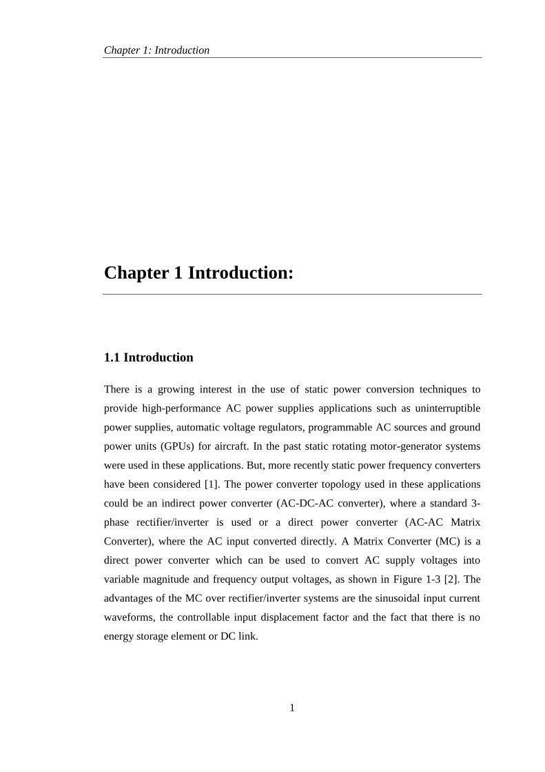
For power supply applications, where different loads needs to be supplied ranging
from balanced, unbalanced and non-linear loads. In such application, 3x3 power
converters will be unable to provide a regulated output voltage. This is because; the
converter needs to be able to deal with zero sequence current in the system.
Ground power units (GPU) are designed to provide a high quality power to aircraft at
airports at 400Hz, 115V. Static power converters are environmentally friendly and
require low maintenance compared to motor generator systems, and the typical rating
are up to 90 kVA per unit [3],[4]. Two possible topologies of a three-phase GPU are
shown in Fig 1-1. Topology (a) has a three-leg converter supplying a four leg Delta-
Star connected transformer while topology (b) has a three phase four leg converter.
Figure 1-1 GPU possible topologies.
The first topology has the advantage of isolation, but the transformer increases the
size and the weight of the system. On the other hand, the second topology is more
compact and has less weight due to the absence of the transformer.
Chapter 1: Introduction
3
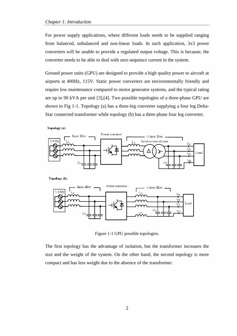
1.2 Power supply aircraft standards
In order to ensure reliable and safe operation of power supply systems, military
authorities have established guidelines on power quality for aircraft applications.
Table 1-1 details the requirements for these systems which are normally 400Hz, three
phase four wire systems. Figure 1-2 shows the allowable output voltage transient
envelope.
Table 1-1 Military standards for aircraft electrical power systems [5].
Steady state voltage 108 to 118 Vrms
Peak transient voltage 271.8 Vrms
Voltage unbalance 3 Vrms
Voltage phase difference 116o to 124o
Voltage distortion 5%
Steady state frequency 393Hz to 407 Hz
Figure 1-2 Envelope of normal 400 Hz and variable frequency AC voltage transient.
Chapter 1: Introduction
4
A 400 Hz system is used in applications where space and weight are important
factors. Due to the higher fundamental frequency, passive components in 400Hz
systems are much smaller (compared to 50Hz, for example); this means that the
system will be lighter and occupy less volume. However, in the design of a converter
with a 400Hz output frequency a high bandwidth controller is required. The reduced
ratio between the converter switching frequency and the fundamental frequency
limits the maximum controller bandwidth. In this case periodic errors and distortion
will exist. A repetitive control (RC) provides a possible solution to minimize these
periodic errors [6], [7].
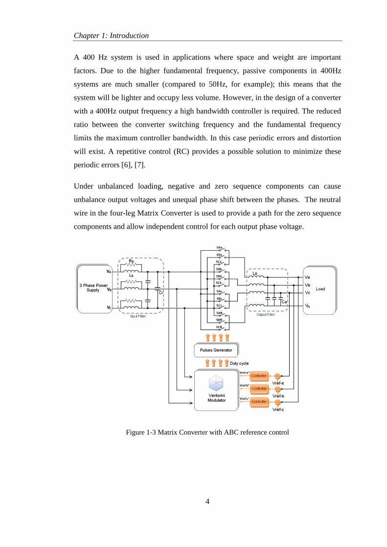
Under unbalanced loading, negative and zero sequence components can cause
unbalance output voltages and unequal phase shift between the phases. The neutral
wire in the four-leg Matrix Converter is used to provide a path for the zero sequence
components and allow independent control for each output phase voltage.
Figure 1-3 Matrix Converter with ABC reference control
Chapter 1: Introduction
5
1.3 Matrix Converters:
A Matrix Converter is an array of bidirectional switches that can directly connect any
input phase to any output phase to create a variable voltage and frequency at the
output. There are several advantages of Matrix Converters such as:
o No DC-link, leading to reduced converter weight and size.
o Simple and compact power circuit.
o The ability to control the output voltages and input currents which results in a
nearly sinusoidal input current with a unity power factor.
o 4 quadrant operations.
The development of Matrix Converters started in early 1980’s after Alesina and
Venturini introduced their basic operation principles [8]. They presented a converter
with an array of bidirectional switches and they introduced the name of Matrix
Converter. The main contribution of Alesina and Venturini was the development of
mathematical analysis that describes the low frequency behaviour of Matrix
Converter. In their basic modulation method the voltage transfer ratio was limited to
0.5, but by the introducing the third harmonics technique the voltage transfer ratio
increased the ratio to 0.86 [9]. The concept of the indirect transfer function technique
was introduced in 1983 by Rodriguez [10]. This method was based on switch
arrangement to switch between the most positive and negative input line using the
same PWM technique as used in standard Voltage source inverters (VSI).
The use of space vectors in the modulation of Matrix Converters was introduced by
Braun in 1983 [11] and Kastner and Rodriguez in 1985 [12]. Then, this was then
extended with Casadei at al paper in 2002 [13], by giving a full Space Vector
modulation strategy that controlled the output voltage and the input power factor
[14]. However instantaneous commutation of the bidirectional switches used in MC’s
was difficult to achieve without overvoltage and current spikes that might destroy the
switches, and this effected the practical implementation of the converters.
Fortunately, the commutation problem was solved by the development of
commutation techniques such as the semisoft current commutation technique [15].
Other advanced commutation strategies were introduced later to allow safe and
Chapter 1: Introduction
6
reliable operation of the switches [16], [17]. Today research activity is mainly
dedicated to studying advanced technological and applications issues such as the
reliable implementation of commutation strategies [18, 19], overvoltage protection
[20, 21], packaging [22], operation under abnormal conditions [4, 23, 24], controller
designs such as dead beat control [25, 26], predictive control [27] ,Genetic
Algorithms [1] and sliding mode control [28] .
1.3.1 Matrix Converter control
The application of digital controller in the field of switch mode power supplies
attracts increased attention due to several advantages. First of all, is the possibility to
implement complex and sophisticated control structure and modify or sometimes to
reprogram the controller, which is not an easy task using analogue controllers.
Secondly, Signal manipulation and taking care of nonlinearities and parameter
variation is very attractive feature of digital controllers. In addition, thermal drifts
and ageing effect do no longer exist in the digital controller. Finally, the rapid
increase in the digital circuit computational power and the continuous reduction of
cost is a great advantage of digital controllers.
1.4 Repetitive control
The concept of repetitive control was originally developed by Inoue et al. in 1980 for
a SISO plants in continuous time domain [29] to track a periodic repetitive signal
with defined period T and was applied successfully to control proton synchrotron
magnet power supply in 1981 [29] . Based on Internal Model Principle proposed by
Francis and Wonham in 1976 [6], any periodic signal with known period T can be
generated by including its generator in the stable close-loop [6]. A repetitive control
system generates a high gain at the periodic signal fundamental frequency and its
integer multiple, therefore a periodic signal can be tracked provided the close loop
system is stable. Repetitive controllers have been widely used in applications
including PWM inverters [30, 31],[32],[33], PWM rectifiers [34-36], Matrix
Converter [4, 37, 38], robotic manipulators [39], disk drive systems [40-42].

Chapter 1: Introduction
7
1.5 Objectives
For a converter with a 400Hz output frequency, a high bandwidth controller is
required. The reduced ratio between the converter switching frequency and the
fundamental frequency limits the controller bandwidth. In this case periodic errors
and distortion can exist.
The main objectives of this project are to:
1. Investigate the use of Venturini modulation to enable the control of a 4-Leg
Matrix Converter.
2. Simulate the 4-leg Matrix Converter using the Saber simulation package.
3. Propose control methods that are able to control the output voltages of the
converter with balanced, unbalanced and non-linear loads.
4. Build a 7.5KW experimental rig to verify the validity of the modulation and
the proposed control systems.
1.6 Thesis outlines
The thesis is organized into 6 chapters. Chapter II presents the fundamentals of
Matrix Converters. This chapter starts by introducing the Matrix Converter structure
including the input and output filters and the bidirectional switches that form the
heart of the power circuit. The chapter also presents Matrix Converter commutation
methods followed by modeling. Finally the chapter presents modulation strategies
including the space vector and Venturini modulation methods.
In chapter III, the control design for the four-leg Matrix Converter is presented.
Modeling of the four-leg Matrix Converter system is shown and both second order
and repetitive control design methods are presented.
In chapter IV, the power converter modeling and simulation methods are shown.
Simulation results for the power converter during balanced, unbalanced and non-
linear loads are presented. Finally, the switching frequency effect on the converter
waveforms is given.

Chapter 1: Introduction
8
Chapter V presents the hardware implementation of a 7.5KW converter prototype.
This chapter describes the overall structure of the prototype converter and explains
the design of each circuit such as the input and output filters, power modules, gate
drive circuit, current direction circuit, clamp circuit measuring circuit and control
platform.
Chapter VI presents the experimental results of prototype converter to demonstrate
the effectiveness of the proposed controller. Experimental results are presented in
this chapter for different load conditions such as balanced, unbalanced and non-linear
loads.
Finally, Chapter VII presents the conclusion of the thesis. This chapter summarizes
the PhD research work findings and introduces future work.
Chapter 2: Fundamentals of matrix converters
9
Chapter 2 Fundamentals of Matrix Converters
2.1 Introduction:
A Matrix Converter is a direct power converter used to convert AC supply voltages
into variable magnitude and frequency output voltages. As shown in Figure 2-1 a
three phase Matrix Converter consists of array of bi-directional switches that are
switched on and off in order to provide variable sinusoidal voltage and frequency to
the load. In this type of converter there is no need to the intermediate DC link power
circuit and this means no large energy storing capacitors. This will increase the
system reliability and reduce the weight and volume for such converters.

Chapter 2: Fundamentals of matrix converters
10
SAa2 SAb2 SAc2 SAN2
SBa2 SBb2 SBc2 SBN2
SCa2 SCb2 SCc2 SCN2
SCa1 SCb1 SCc1 SCN1
SBa1 SBb1 SBc1 SBN1
SAa1 SAb1 SAc1 SAN1
Rs
LsCs
Lo
Co
Load
Va
Vc
Vb
n
Input Filter
Output Filter
Bi-Directional
SwitchVA
VB
VC
Figure 2-1 Four-leg Matrix Converter system
2.2 Matrix Converter structure
In this section, the main components of the Matrix Converter will be described. First,
the input filter structure and design is investigated. After that the bidirectional power
switches are presented. Then the output filter design is discussed. Finally, the clamp
circuit that is used to ensure safe operation of the Matrix Converter is also described.
2.2.1 Input filter
In power converters input filters are used in order to improve the input current
quality and to reduce the input voltage distortion. It acts as an interface between the
input power supply and the converter. There are several important features for using
the input filter such as [43, 44]:
- it helps to avoid the significant changes of the input supply voltage during
each PWM cycle.

Chapter 2: Fundamentals of matrix converters
11
- it helps to prevent the unwanted harmonics from flowing into the input power
supply.
- it helps to satisfy the electromagnetic interference requirements.
- it helps to protect the converter from transients that appear in the input supply
side.
The design of the input filter has to accomplish the following [45]:
- the cut-off frequency of the input filter should be at least one decade above
the supply frequency and one decade bellow the switching frequency.
- minimize the voltage drop on the filter inductance at the rated current in order
to provide the highest converter voltage transfer ratio.
- minimization of the displacement factor between the supply voltage and the
voltages applied to the matrix converter.
- minimization of the ripples in the supply current and the capacitors voltage.
- control the power losses in the damping resistor.
There are a number of different filter topologies can be used for the MC [46]. Among
these is the second order LC filter shown in Figure 2-2; it is a common practice to
use this topology in many MC applications in view of the low number of components
and the satisfactory frequency response that can be achieved [45-50]. Figure 2-2
shows the single phase LCR filter used in this work.
Cs
Ls
RsInput filter
3 Phase
Input
Voltage
SAa2 SAN2
SBa2
SCa2 SCN2
SCa1 SCN1
SBa1
SAa1 SAN1
Figure 2-2 Input filter circuit.
The transfer function of the single phase diagram shown in Figure 2-3 of the input
filter can be described by [51]:
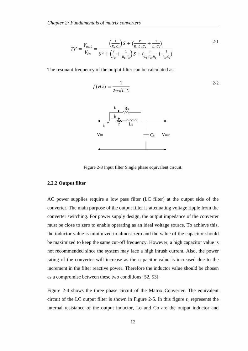
Chapter 2: Fundamentals of matrix converters
12
(
)
(
)
2-1
The resonant frequency of the output filter can be calculated as:
√
2-2
Rs
Ls
Cs VoutVin
is
ib
ia
r
Figure 2-3 Input filter Single phase equivalent circuit.
2.2.2 Output filter
AC power supplies require a low pass filter (LC filter) at the output side of the
converter. The main purpose of the output filter is attenuating voltage ripple from the
converter switching. For power supply design, the output impedance of the converter
must be close to zero to enable operating as an ideal voltage source. To achieve this,
the inductor value is minimized to almost zero and the value of the capacitor should
be maximized to keep the same cut-off frequency. However, a high capacitor value is
not recommended since the system may face a high inrush current. Also, the power
rating of the converter will increase as the capacitor value is increased due to the
increment in the filter reactive power. Therefore the inductor value should be chosen
as a compromise between these two conditions [52, 53].
Figure 2-4 shows the three phase circuit of the Matrix Converter. The equivalent
circuit of the LC output filter is shown in Figure 2-5. In this figure ro represents the
internal resistance of the output inductor, Lo and Co are the output inductor and
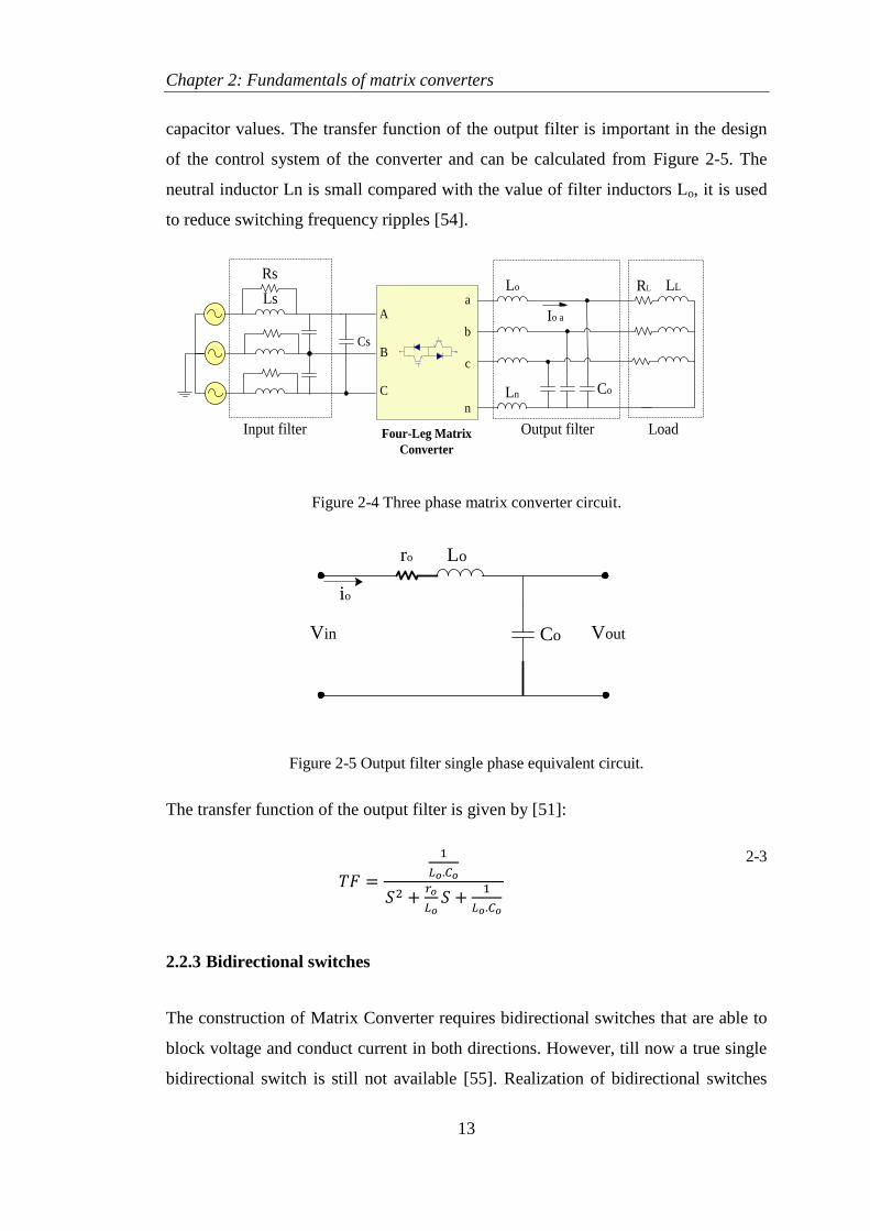
Chapter 2: Fundamentals of matrix converters
13
capacitor values. The transfer function of the output filter is important in the design
of the control system of the converter and can be calculated from Figure 2-5. The
neutral inductor Ln is small compared with the value of filter inductors Lo, it is used
to reduce switching frequency ripples [54].
Co
LLRL
Io a
Lo
Ln
A
B
C
Ls
Rs
Cs
Input filter
a
b
c
n
Output filterFour-Leg Matrix
Converter
Load
Figure 2-4 Three phase matrix converter circuit.
Lo
Co VoutVin
io
ro
Figure 2-5 Output filter single phase equivalent circuit.
The transfer function of the output filter is given by [51]:
2-3
2.2.3 Bidirectional switches
The construction of Matrix Converter requires bidirectional switches that are able to
block voltage and conduct current in both directions. However, till now a true single
bidirectional switch is still not available [55]. Realization of bidirectional switches

Chapter 2: Fundamentals of matrix converters
14
are therefore based on a combination of discrete devices as shown in Figure 2-6.
Different bidirectional switch arrangements have been proposed in the literature [15,
56].
2.2.3.1 Diode bridge arrangement
It is possible to build a bidirectional switch using one switching device such as an
IGBT, MCT or IGCT, as shown in Figure 2-6 (A). The main advantages of this
configuration are that only one gate drive circuit is required to switch the device on
and off. However, because there are three devices conducting at the same time
conduction losses will be large.
A B C D
Figure 2-6 Bidirectional switches configuration
2.2.3.2 Common emitter configuration
The common emitter configuration is shown in Figure 2-6 (B). This arrangement
consists of two diodes and two IGBT’s connected in anti-parallel configuration. One
diode and one IGBT are conducting at any time. These diodes are included to
provide reverse blocking capabilities. The advantages of this configuration are lower
conduction losses and independent control of positive and negative currents.
2.2.3.3 Common collector configuration
The common collector configuration is shown in Figure 2-6 (C). The conduction
losses are similar to the common emitter configuration. However, this configuration
is not feasible in very large practical systems since the inductance between
commutation cells causes a problem [55]
Chapter 2: Fundamentals of matrix converters
15
2.2.3.4 Anti-parallel reverse blocking IGBTs
It is possible to build a bidirectional switch by simply connecting two reverse
blocking devices in anti-parallel as shown in Figure 2-6 (D). In this configuration the
efficiency may be improved and a compact converter size is possible to build.
However, to date IGBTs showed poor reverse blocking capabilities and this
prevented wide spread use of this configuration.
The common emitter configuration is the preferred solution as it is possible to control
the direction of the current and conduction losses are lower since only two devices
carry the current at any one time. One disadvantage of this configuration is that each
bidirectional switch requires an isolated power supply for the gate drive unit [55].
2.3 Matrix Converter Current Commutation
Current transfer from one phase into another is difficult to achieve in Matrix
Converters due to the fact that there is no a natural freewheeling path for the current.
Therefore, controlling the current commutation between bidirectional switches is an
important task. Two important rules need to be considered in the commutation:
For each output phase, do not switch two switches at the same time. Because
this will result in a high short circuit that will destroy the converter.
Do not switch off two switches in the output phase at the same time, this will
cause an over-voltage. Always allow a path for the inductive load current to
flow.
There is several commutation techniques proposed in the literature such as simple
and advanced commutation methods [55, 57].
2.3.1 Simple Commutation Methods
Simple commutation methods such as overlap, dead time and semi soft commutation
are discussed below. In the overlap current commutation method the incoming
switch is turned on before the outgoing switch is turned off. This will result in a short
circuit between the supply phases. Extra supply inductance must be used to limit the
Chapter 2: Fundamentals of matrix converters
16
current but, this method is rarely used [16]. In the dead time current commutation
method the outgoing switch is turned off before the incoming switch is turned on.
This method will introduce a dead time in which there is no a path for the inductive
load current. Therefore a snubber circuit is required to provide a path for the current.
This method is poor due to the wasted energy in the snubber circuit.
2.3.2 Soft switching techniques
Soft switching technique such as resonant switch circuits [58, 59] and auxiliary
resonant circuits [60], have been introduced in order to reduce switching losses and
improve efficiency in power converters. However, in Matrix Converters resonant
techniques have extra benefit of solving commutation problem. All these circuits
increase the number of components being used in Matrix Converter and this also
leads to additional conduction losses.
2.3.3 Advanced commutation methods
For a reliable safe commutation a specific sequence must be adopted without short
circuiting the input voltages or breaking the inductive load current. The first current
commutation method that does not break the previous rules was proposed in [15] and
named semi-soft commutation method or four-step commutation method. These
advanced commutation methods are based on the measurement of the load current
direction or on the input voltage magnitude or both [57]. In this project current
commutation based on the output current direction was adopted.
2.3.4 Output current direction based commutation method.
This commutation method is based on the load current direction. The load current
direction is assumed to be in the direction shown in Figure 2-7, switch SA is
assumed to be switched on.
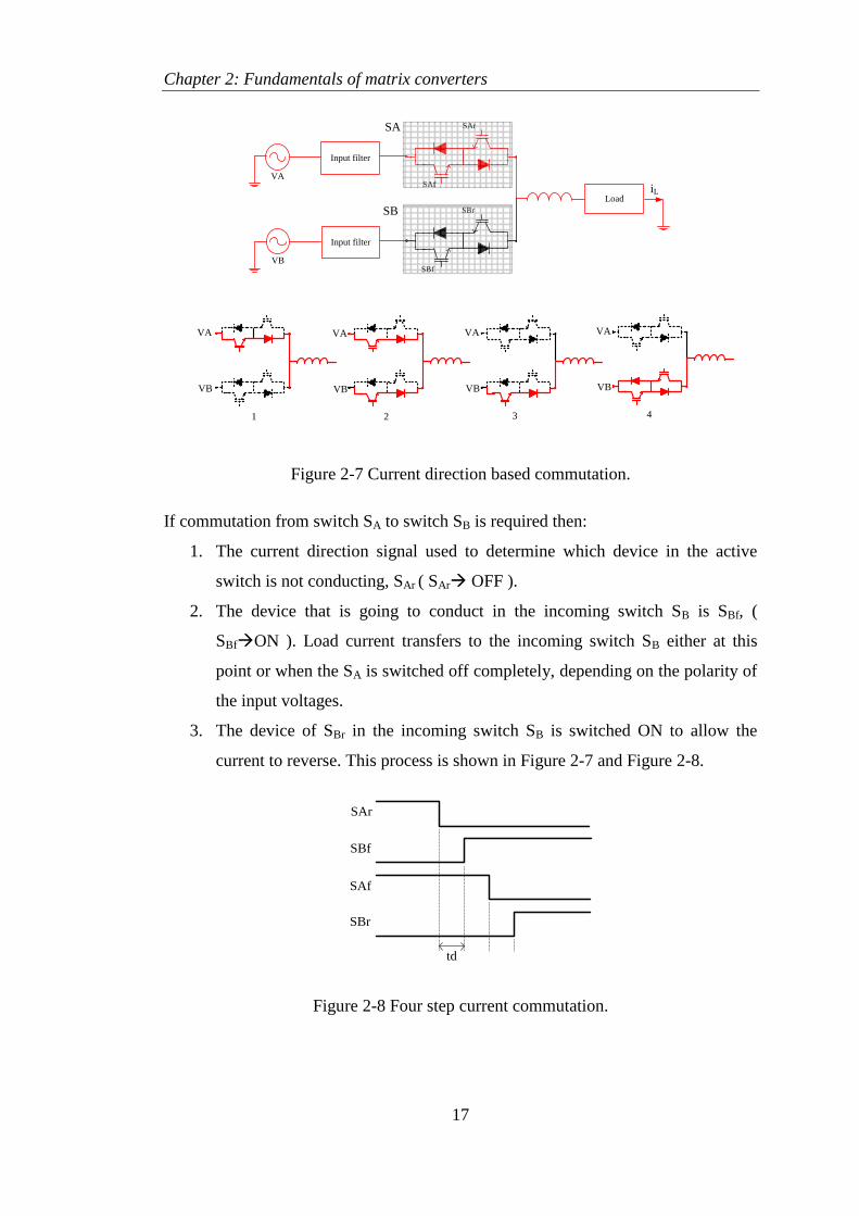
Chapter 2: Fundamentals of matrix converters
17
VA
Input filter
VB
Input filter
Load
SAf
SAr
SBf
SBr
SA
SB
1 2 3 4
VA
VB
VA
VB
VA
VB
VA
VB
iL
Figure 2-7 Current direction based commutation.
If commutation from switch SA to switch SB is required then:
1. The current direction signal used to determine which device in the active
switch is not conducting, SAr ( SAr OFF ).
2. The device that is going to conduct in the incoming switch SB is SBf, (
SBfON ). Load current transfers to the incoming switch SB either at this
point or when the SA is switched off completely, depending on the polarity of
the input voltages.
3. The device of SBr in the incoming switch SB is switched ON to allow the
current to reverse. This process is shown in Figure 2-7 and Figure 2-8.
SAr
SBf
SAf
SBr
td
Figure 2-8 Four step current commutation.
Chapter 2: Fundamentals of matrix converters
18
Figure 2-9 shows the state diagram of the current commutation according to the load
current direction.
SAr =1
SBf =0
SAf =1
SBr =0
SAr =0
SBf =0
SAf =1
SBr =0
SAr =1
SBf =0
SAf =0
SBr =0
SAr =0
SBf =1
SAf =1
SBr =0
SAr =1
SBf =0
SAf =0
SBr =1
SAr =0
SBf =1
SAf =0
SBr =0
SAr =0
SBf =0
SAf =0
SBr =1
SAr =0
SBf =1
SAf =0
SBr =1
iL>0
iL<0
Steady State Transitional state Steady State
Figure 2-9 Four step current commutation
2.4 Matrix Converter modulation strategies
There are a number of possible modulation techniques that can be used for Matrix
Converter control. The optimal modulation strategy should minimise the input
current and output voltage harmonic distortion and device power losses [61].
The most relevant control and modulation methods developed for the MCs are the
Venturini method, the scalar method developed by Roy and the space-vector
modulation (SVM) [9, 11, 12]. In the Venturini method the output voltage is
obtained by the product of the input voltage and the transfer matrix. While in the Roy
scalar modulation the instantaneous voltage ratio of specific input phase voltages is
used to generate the active and zero states of the converter’s switches. Comparisons
between the SVM and the Venturini modulation methods show that switching losses
are lower for the SVM method; however the Venturini modulation method shows
better performance in terms of input current and output voltage harmonics. In this
work the Venturini method is preferred because it deals with scalar quantities rather
than vectors, and this is important when controlling unbalanced or non-linear loads
[62, 63].
Chapter 2: Fundamentals of matrix converters
19
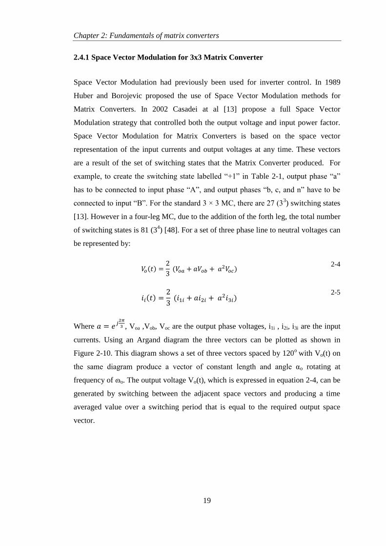
2.4.1 Space Vector Modulation for 3x3 Matrix Converter
Space Vector Modulation had previously been used for inverter control. In 1989
Huber and Borojevic proposed the use of Space Vector Modulation methods for
Matrix Converters. In 2002 Casadei at al [13] propose a full Space Vector
Modulation strategy that controlled both the output voltage and input power factor.
Space Vector Modulation for Matrix Converters is based on the space vector
representation of the input currents and output voltages at any time. These vectors
are a result of the set of switching states that the Matrix Converter produced. For
example, to create the switching state labelled “+1” in Table 2-1, output phase “a”
has to be connected to input phase “A”, and output phases “b, c, and n” have to be
connected to input “B”. For the standard 3 × 3 MC, there are 27 (33) switching states
[13]. However in a four-leg MC, due to the addition of the forth leg, the total number
of switching states is 81 (34) [48]. For a set of three phase line to neutral voltages can
be represented by:
2-4
2-5
Where
, Voa ,Vob, Voc are the output phase voltages, i1i , i2i, i3i are the input
currents. Using an Argand diagram the three vectors can be plotted as shown in
Figure 2-10. This diagram shows a set of three vectors spaced by 120o
with Vo(t) on
the same diagram produce a vector of constant length and angle αo rotating at
frequency of ɷo. The output voltage Vo(t), which is expressed in equation 2-4, can be
generated by switching between the adjacent space vectors and producing a time
averaged value over a switching period that is equal to the required output space
vector.
Chapter 2: Fundamentals of matrix converters
20
Figure 2-10 SVM Vectors for a Balanced 3-Phase
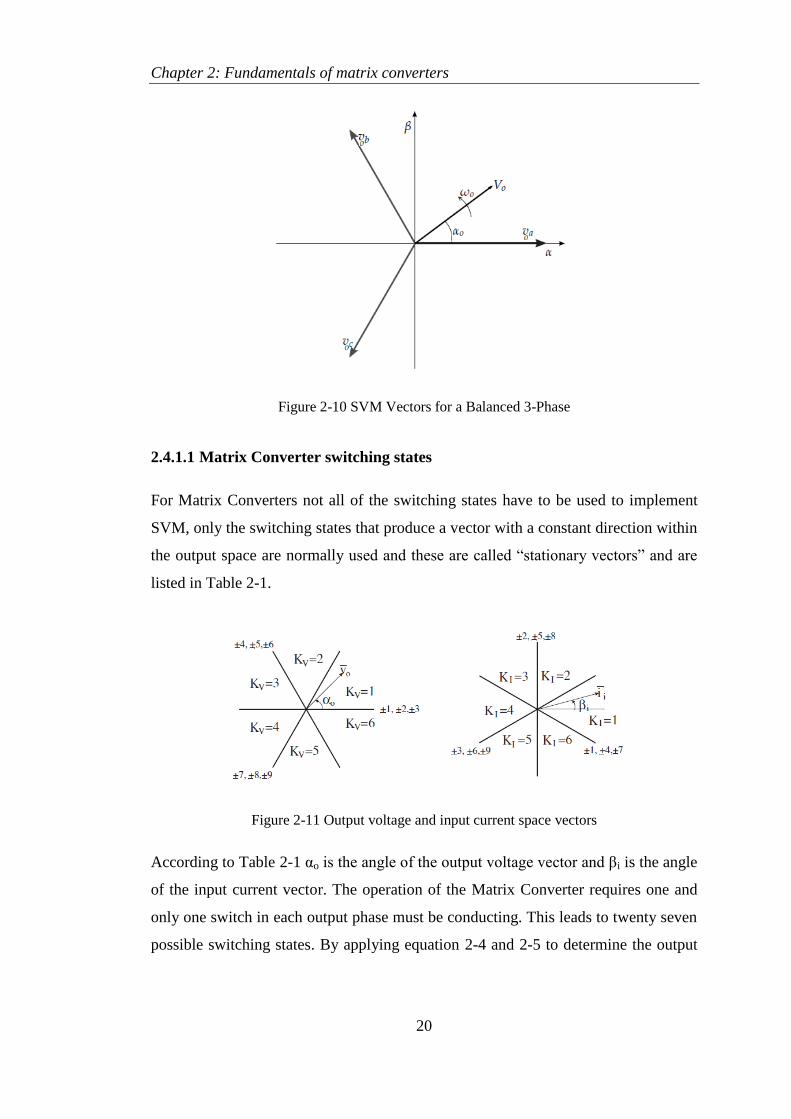
2.4.1.1 Matrix Converter switching states
For Matrix Converters not all of the switching states have to be used to implement
SVM, only the switching states that produce a vector with a constant direction within
the output space are normally used and these are called “stationary vectors” and are
listed in Table 2-1.
Figure 2-11 Output voltage and input current space vectors
According to Table 2-1 αo is the angle of the output voltage vector and βi is the angle
of the input current vector. The operation of the Matrix Converter requires one and
only one switch in each output phase must be conducting. This leads to twenty seven
possible switching states. By applying equation 2-4 and 2-5 to determine the output

Chapter 2: Fundamentals of matrix converters
21
voltage and the input current vectors, the magnitude and the phase of these vectors
for all possible combinations are given in Table 2-1
Table 2-1 Switching states of three phase Matrix Converter[57] .
Group 1 vectors are split into three sub-groups as shown in table 2.1. These six states
produce a vector in a defined direction. For the three sub-groups the directions are
displaced by 120o.
2.4.1.2 Switching state selection
Using the eighteen fixed direction and three null vector combinations, it is possible
to generate the required output voltage vector and the required input current

Chapter 2: Fundamentals of matrix converters
22
direction. Figure 2-11 shows the output line to neutral voltage vector and input
current vector direction generated by the fixed eighteen direction configurations [13].
As shown in Figure 2-11, Kv is the sector that contains the output voltage vectors. Ki
is the sector that contains the input current vector. Using table 2.2 and 2.3 it can be
seen that for any combination of output voltage and input current sectors, four
configurations can be identified that produce output voltage vectors and input current
vectors laying adjacent to the desired vectors.
Table 2-2 Selection of switching configuration according to output voltage and input current
sectors [13].
The required modulation duty cycles for the switching configurations I, II, III and IV
are giving by equation 2-6 to 2-10
√
(
)
2-6
√
(
)
2-7
√
(
)
2-8
√
(
)
2-9
Where are the angles of the output voltage and input current vectors
measured from the bisecting line of the corresponding sectors. is the input phase
displacement angle.
Chapter 2: Fundamentals of matrix converters
23
For unity input power factor operation
2-10
If double sided modulation is used then is distributed in the modulation period by
two equal parts [13, 51].
2.4.2 Space Vector Modulation for 3x4 Matrix Converter
Matrix Converter modulation is based on the space vector representation of the input
and output voltages and currents at any one instant. This section will present a brief
summery on the space vector modulation for the three phase four-leg matrix
converter.
2.4.2.1 Input voltage and current plane
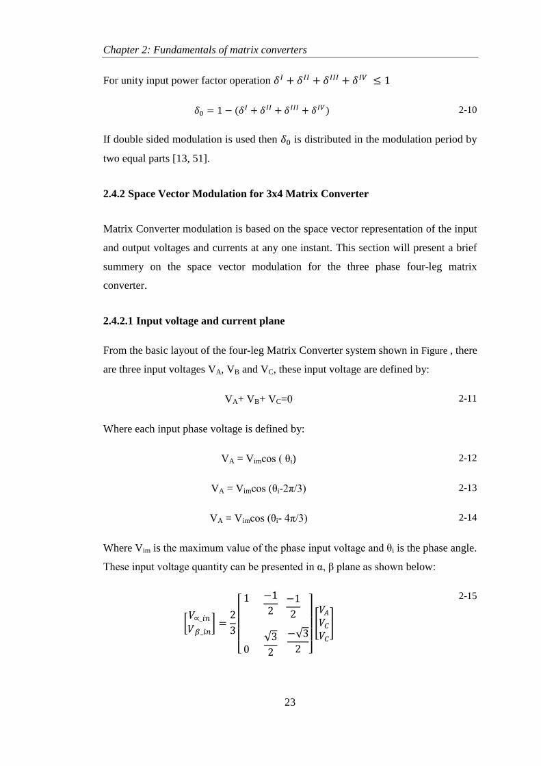
From the basic layout of the four-leg Matrix Converter system shown in Figure , there
are three input voltages VA, VB and VC, these input voltage are defined by:
VA+ VB+ VC=0 2-11
Where each input phase voltage is defined by:
VA = Vimcos ( θi) 2-12
VA = Vimcos (θi-2π/3) 2-13
VA = Vimcos (θi- 4π/3) 2-14
Where Vim is the maximum value of the phase input voltage and θi is the phase angle.
These input voltage quantity can be presented in α, β plane as shown below:
[
]
[
√
√
]
[
]
2-15
Chapter 2: Fundamentals of matrix converters
24
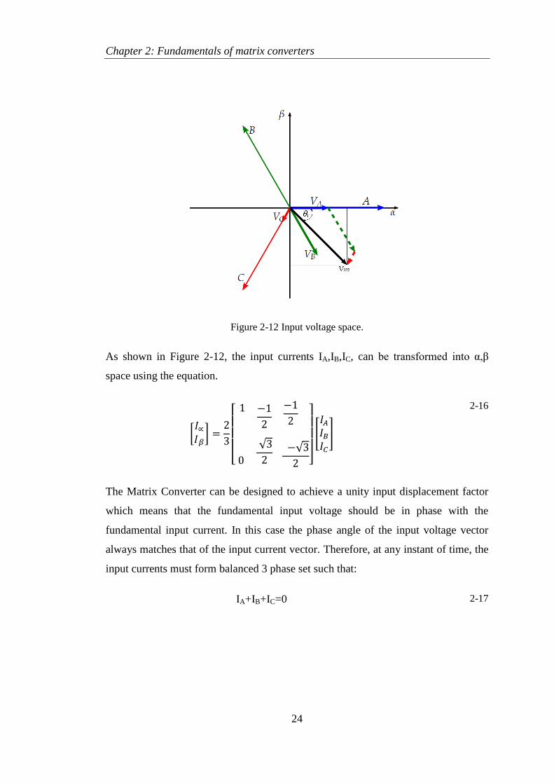
Figure 2-12 Input voltage space.
As shown in Figure 2-12, the input currents IA,IB,IC, can be transformed into α,β
space using the equation.
[
]
[
√
√
]
[
]
2-16
The Matrix Converter can be designed to achieve a unity input displacement factor
which means that the fundamental input voltage should be in phase with the
fundamental input current. In this case the phase angle of the input voltage vector
always matches that of the input current vector. Therefore, at any instant of time, the
input currents must form balanced 3 phase set such that:
IA+IB+IC=0 2-17
Chapter 2: Fundamentals of matrix converters
25
2.4.2.2 Switching States for the Four-Leg Matrix Converter
The switching states are the states which obey the fundamental rules of the Matrix
Converter which are that the input phases cannot be shorted together and no output
leg can be open circuit. For the standard 3x3 Matrix Converter there are 27 (33)
possible switching states [4]. However, using the four-leg Matrix Converter the total
number of the switching states increases to 81 (34). All of these switching states are
shown in Table 2-3 and Table 2-4. As shown in a 3x3 Matrix Converter [13], not all
of the switching states are normally used for space vector modulation. So only th
states that produce a vector with constant direction within the output space are to be
used and these are called the stationary vectors. For the Matrix Converter systems
there are 3 switching state categories:
Rotating vectors states: in this category all the three input phases are connected to
the output. This means that two different line to line voltages are present between the
output phases and in this case the resultant vectors change in magnitude and
direction. This category is presented in Table 2-3.
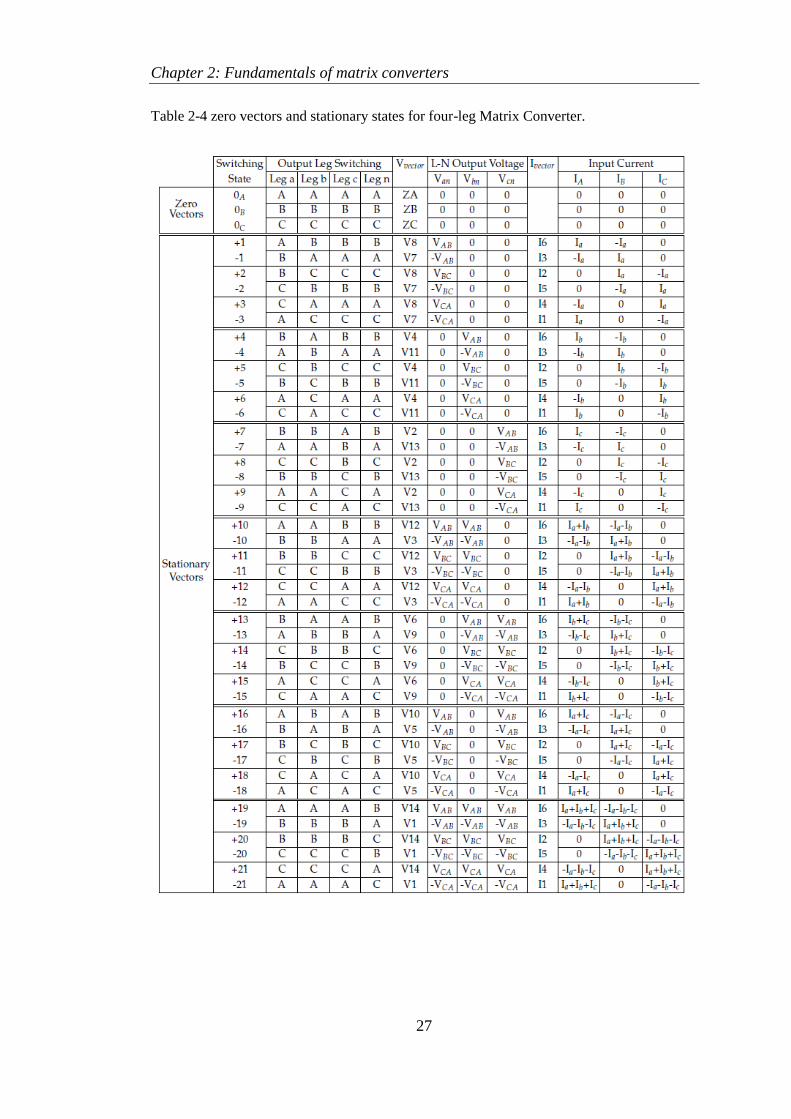
Stationary vectors states: any two phases of the input voltages are connected to the
output legs at any moment in time. This category is the one of interest as the output
voltage generated are either zero or the line to line voltage between the two
connected phases. This category is shown in Table 2-4
Zero vector states: in this category all the four output phases are connected to a
single input phase. When the four output phases are connected to one single input
phase the voltage between the output phases becomes zero. These vectors are
important as they allow a zero state to be applied to the output without disconnecting
the output legs from the input phases. This category can be seen at the top of
Table 2-4.

Chapter 2: Fundamentals of matrix converters
26
Table 2-3 Rotating vector states for four-leg Matrix Converter.
Chapter 2: Fundamentals of matrix converters
27
Table 2-4 zero vectors and stationary states for four-leg Matrix Converter.
Chapter 2: Fundamentals of matrix converters
28
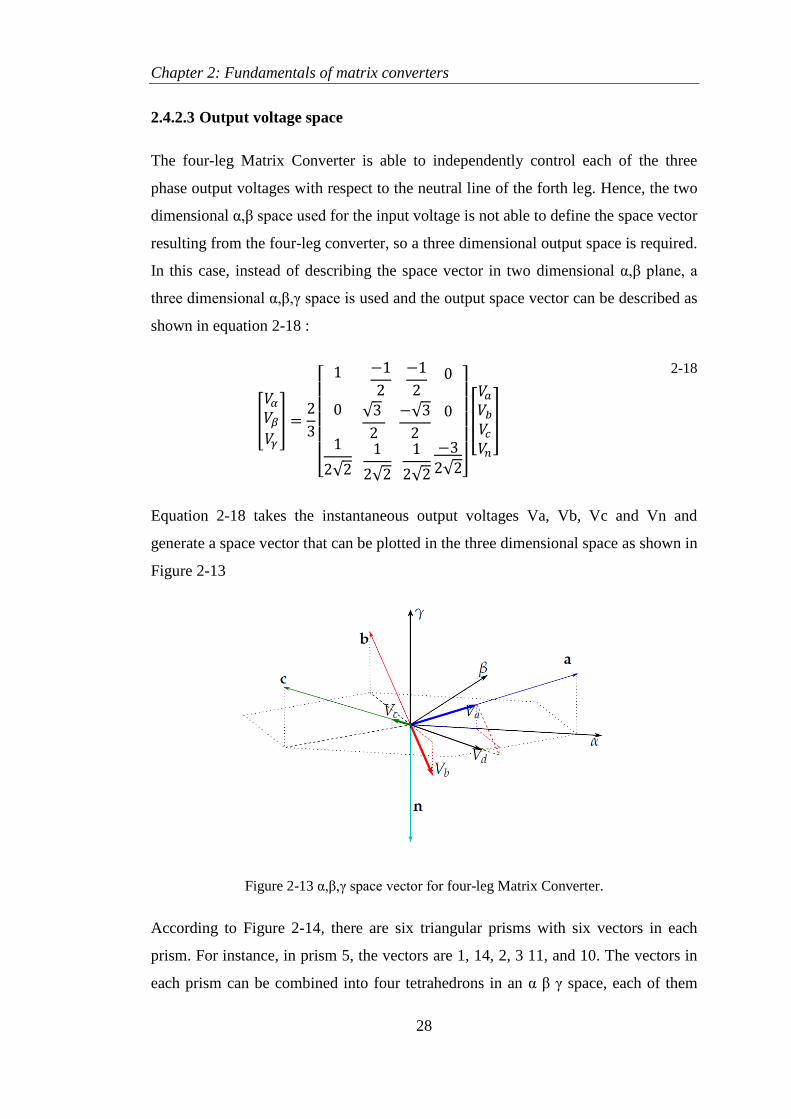
2.4.2.3 Output voltage space
The four-leg Matrix Converter is able to independently control each of the three
phase output voltages with respect to the neutral line of the forth leg. Hence, the two
dimensional α,β space used for the input voltage is not able to define the space vector
resulting from the four-leg converter, so a three dimensional output space is required.
In this case, instead of describing the space vector in two dimensional α,β plane, a
three dimensional α,β,γ space is used and the output space vector can be described as
shown in equation 2-18 :
[
]
[
√
√
√
√
√
√ ]
[
]
2-18
Equation 2-18 takes the instantaneous output voltages Va, Vb, Vc and Vn and
generate a space vector that can be plotted in the three dimensional space as shown in
Figure 2-13
Figure 2-13 α,β,γ space vector for four-leg Matrix Converter.
According to Figure 2-14, there are six triangular prisms with six vectors in each
prism. For instance, in prism 5, the vectors are 1, 14, 2, 3 11, and 10. The vectors in
each prism can be combined into four tetrahedrons in an α β γ space, each of them
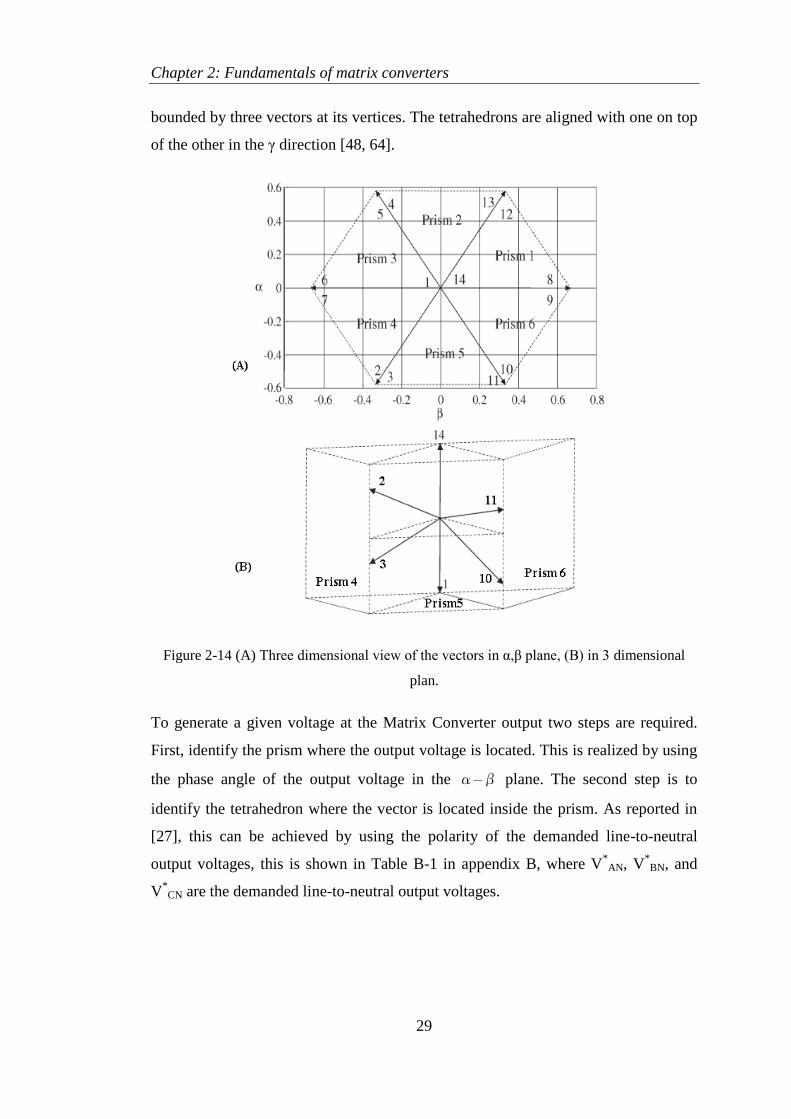
Chapter 2: Fundamentals of matrix converters
29
bounded by three vectors at its vertices. The tetrahedrons are aligned with one on top
of the other in the γ direction [48, 64].
Figure 2-14 (A) Three dimensional view of the vectors in α,β plane, (B) in 3 dimensional
plan.
To generate a given voltage at the Matrix Converter output two steps are required.
First, identify the prism where the output voltage is located. This is realized by using
the phase angle of the output voltage in the α–β plane. The second step is to
identify the tetrahedron where the vector is located inside the prism. As reported in
[27], this can be achieved by using the polarity of the demanded line-to-neutral
output voltages, this is shown in Table B-1 in appendix B, where V*
AN, V*BN, and
V*CN are the demanded line-to-neutral output voltages.
Chapter 2: Fundamentals of matrix converters
30
2.4.3 Principles of the Venturini modulation method
Matrix Converter modulation strategy was first introduced by Venturini and Alesina
[2, 8, 55, 65]. The purpose of this modulation is to produce a train of pulses that
controls Matrix Converter bidirectional switches to convert the fixed amplitude and
frequency input voltage into variable amplitude and frequency sinusoidal voltage.
The voltage transfer ratio is the ratio between the target output voltage and the input
voltage, initially this ratio was limited to 0.5 in the basic Venturini modulation [8],
as shown in Figure 2-15.
2.4.3.1 Basic Venturini modulation method
The modulation problem assumes that a set of sinusoidal output voltages and input
currents as shown in equations 2-19 and 2-20. The input voltage can be expressed as:
Vi(t)=[
]=[
]
While the output current is represented by:
Io(t)= [
]
The main objective now is to find a modulation matrix, M(t), such that equation 2-19
and 2-20 are satisfied, as well as the Matrix Converter constraints in equation .
VoN(t)= [
]
2-19
Ii(t)=
[
]
2-20
Where q is the voltage transfer ratio, and are the input and the output
frequencies and and are the input and output displacement angles respectively.
Chapter 2: Fundamentals of matrix converters
31
there are two solutions to this modulation problem which were found by Venturini
[65]. These solutions are represented by:
[ ]
[
(
)
(
)
(
)
(
)
(
)
(
)
]
2-21
Where
[ ]
[
(
)
(
)
(
)
(
)
(
)
(
)]
2-22
With
According to the solution in equation 2-21, the phase displacement of the input and
the output are the same because whereas the solution in equation 2-22 yields
which give a negative phase displacement at the input. Combining the two
solutions provides the means for input displacement factor control.
M(t)= [ ] [ ] 2-23
Setting gives unity input displacement factor regardless of the load
displacement factor. Other possibilities exist, through the choice of and , to
have a leading displacement factor (capacitive) at the input with a lagging (inductive)
load at the output and vice versa.
For the modulation functions can be expressed in the compact form:
(
) for K=A,B,C and j=a,b,c,N
2-24
Chapter 2: Fundamentals of matrix converters
32
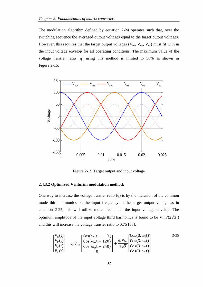
The modulation algorithm defined by equation 2-24 operates such that, over the
switching sequence the averaged output voltages equal to the target output voltages.
However, this requires that the target output voltages (Voa, Vob, Voc) must fit with in
the input voltage envelop for all operating conditions. The maximum value of the
voltage transfer ratio (q) using this method is limited to 50% as shown in
Figure 2-15.
Figure 2-15 Target output and input voltage
2.4.3.2 Optimized Venturini modulation method:
One way to increase the voltage transfer ratio (q) is by the inclusion of the common
mode third harmonics on the input frequency in the target output voltage as in
equation 2-25, this will utilize more area under the input voltage envelop. The
optimum amplitude of the input voltage third harmonics is found to be Vim/(2√ )
and this will increase the voltage transfer ratio to 0.75 [55].
[
] [
]
√ [
]
2-25
0 0.005 0.01 0.015 0.02 0.025-150
-100
-50
0
50
100
150
Time
Vo
ltag
e
V
inAV
inBV
inCV
oaV
obV
oc
Chapter 2: Fundamentals of matrix converters
33
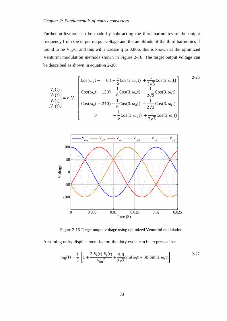
Further utilization can be made by subtracting the third harmonics of the output
frequency from the target output voltage and the amplitude of the third harmonics if
found to be Vim/6, and this will increase q to 0.866, this is known as the optimized
Venturini modulation methods shown in Figure 2-16. The target output voltage can
be described as shown in equation 2-26:
[
]
[
√
√
√
√ ]
2-26
Figure 2-16 Target output voltage using optimized Venturini modulation.
Assuming unity displacement factor, the duty cycle can be expressed as:
[
√ β ]
2-27
0 0.005 0.01 0.015 0.02 0.025
-100
-50
0
50
100
Time (S)
Vo
ltag
e
V
inAV
inBV
inCV
trgAV
trgBV
trgC

Chapter 2: Fundamentals of matrix converters
34
where
i= A, B, C and j =a, b, c,N
β π
π
During unbalanced load condition the value of q will be different for each phase.
Where qa=Va/Vim, qb=Vb/Vim and qc=Vc/Vim.
2.4.4 Switching Sequence of the Four-Leg Matrix Converter
The basic switching sequence for a Matrix Converter is shown in Figure 2-17. This
switching sequence can be changed to achieve lower converter losses and to reduce
the amount of harmonics in the output voltage and input current waveforms.
2.4.4.1 Basic Switching Sequence:
According to the four-leg Matrix Converter circuit shown in Figure 2-1 each output
phase is connected to the input phases for specific time. The switching sequence is
fixed to A-B-C in a single side switching. For example output phase a is connected to
input phase A for tAa, and to phase B for tBa and to phase C for tCa, to produce the
output voltage Va.
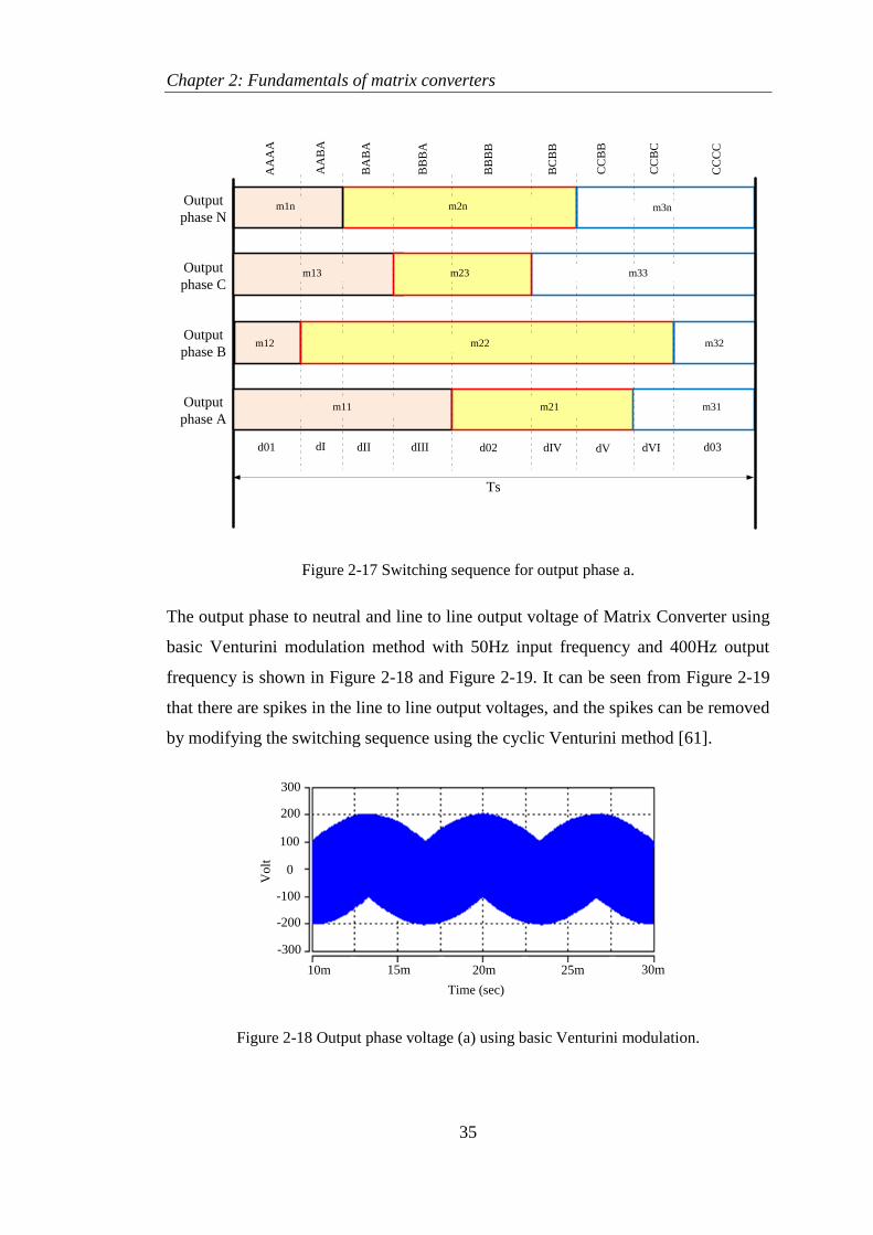
Chapter 2: Fundamentals of matrix converters
35
d01 dI dII dIII d02 dIV dV dVI d03
m1n m2n m3n
m13 m23 m33
m12 m22 m32
m11 m21 m31
Ts
AA
AA
AA
BA
BA
BA
BB
BA
BB
BB
BC
BB
CC
BC
CC
BB
CC
CC
Output
phase N
Output
phase C
Output
phase B
Output
phase A
Figure 2-17 Switching sequence for output phase a.
The output phase to neutral and line to line output voltage of Matrix Converter using
basic Venturini modulation method with 50Hz input frequency and 400Hz output
frequency is shown in Figure 2-18 and Figure 2-19. It can be seen from Figure 2-19
that there are spikes in the line to line output voltages, and the spikes can be removed
by modifying the switching sequence using the cyclic Venturini method [61].
-200
-100
0
100
200
Volt
10m 15m 20m 30m25m
Time (sec)
300
-300
Figure 2-18 Output phase voltage (a) using basic Venturini modulation.
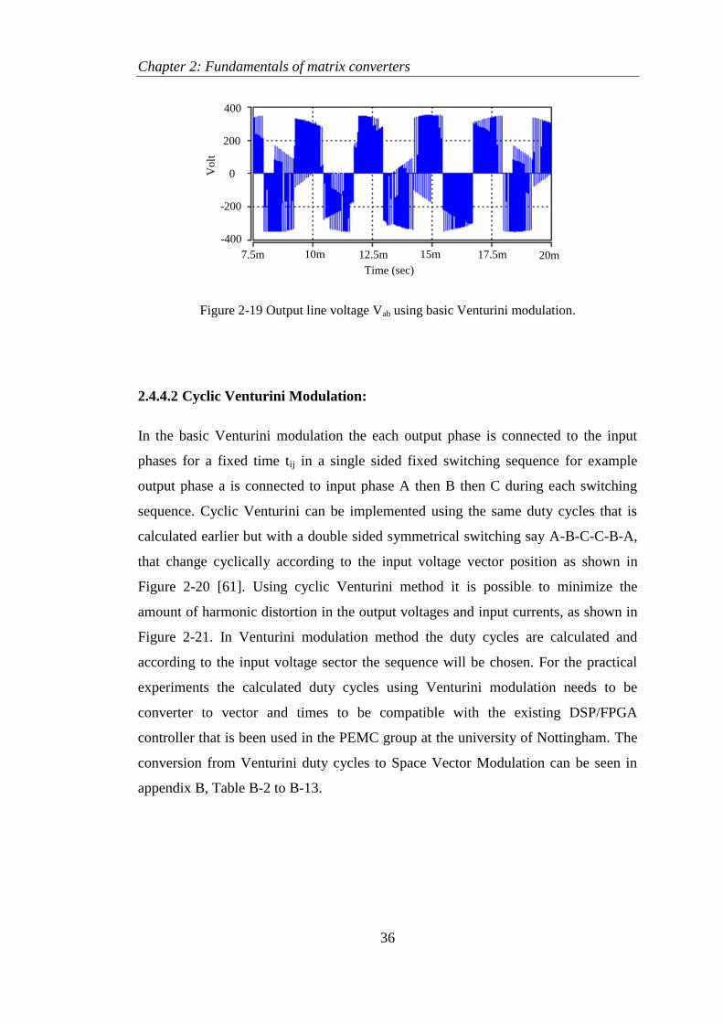
Chapter 2: Fundamentals of matrix converters
36
7.5m 10m 12.5m 15m 17.5m 20m
-400
-200
0
200
400
Vo
lt
Time (sec)
Figure 2-19 Output line voltage Vab using basic Venturini modulation.
2.4.4.2 Cyclic Venturini Modulation:
In the basic Venturini modulation the each output phase is connected to the input
phases for a fixed time tij in a single sided fixed switching sequence for example
output phase a is connected to input phase A then B then C during each switching
sequence. Cyclic Venturini can be implemented using the same duty cycles that is
calculated earlier but with a double sided symmetrical switching say A-B-C-C-B-A,
that change cyclically according to the input voltage vector position as shown in
Figure 2-20 [61]. Using cyclic Venturini method it is possible to minimize the
amount of harmonic distortion in the output voltages and input currents, as shown in
Figure 2-21. In Venturini modulation method the duty cycles are calculated and
according to the input voltage sector the sequence will be chosen. For the practical
experiments the calculated duty cycles using Venturini modulation needs to be
converter to vector and times to be compatible with the existing DSP/FPGA
controller that is been used in the PEMC group at the university of Nottingham. The
conversion from Venturini duty cycles to Space Vector Modulation can be seen in
appendix B, Table B-2 to B-13.
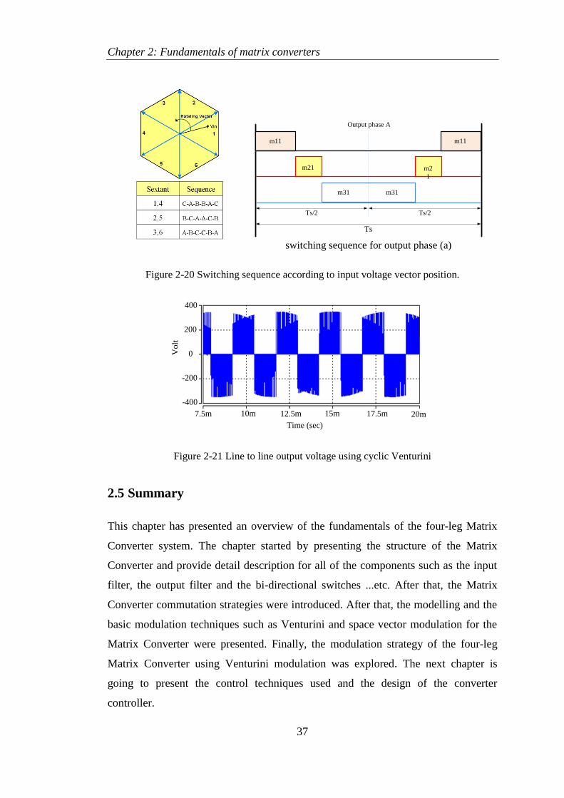
Chapter 2: Fundamentals of matrix converters
37
Ts
m11
m21
m21
Ts/2 Ts/2
m31
m2
1
m11
m31
Output phase A
switching sequence for output phase (a)
Figure 2-20 Switching sequence according to input voltage vector position.
7.5m 10m 12.5m 15m 17.5m 20m
-400
-200
0
200
400
Vo
lt
Time (sec)
Figure 2-21 Line to line output voltage using cyclic Venturini
2.5 Summary
This chapter has presented an overview of the fundamentals of the four-leg Matrix
Converter system. The chapter started by presenting the structure of the Matrix
Converter and provide detail description for all of the components such as the input
filter, the output filter and the bi-directional switches ...etc. After that, the Matrix
Converter commutation strategies were introduced. After that, the modelling and the
basic modulation techniques such as Venturini and space vector modulation for the
Matrix Converter were presented. Finally, the modulation strategy of the four-leg
Matrix Converter using Venturini modulation was explored. The next chapter is
going to present the control techniques used and the design of the converter
controller.
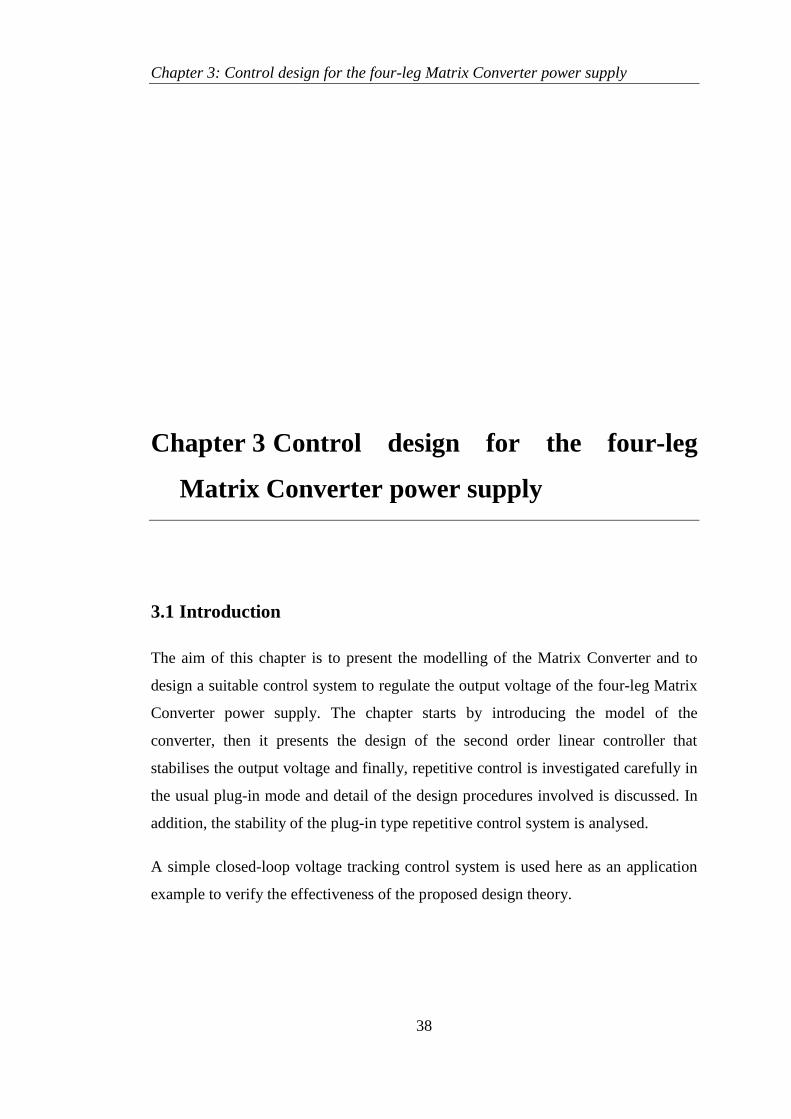
Chapter 3: Control design for the four-leg Matrix Converter power supply
38
Chapter 3 Control design for the four-leg
Matrix Converter power supply
3.1 Introduction
The aim of this chapter is to present the modelling of the Matrix Converter and to
design a suitable control system to regulate the output voltage of the four-leg Matrix
Converter power supply. The chapter starts by introducing the model of the
converter, then it presents the design of the second order linear controller that
stabilises the output voltage and finally, repetitive control is investigated carefully in
the usual plug-in mode and detail of the design procedures involved is discussed. In
addition, the stability of the plug-in type repetitive control system is analysed.
A simple closed-loop voltage tracking control system is used here as an application
example to verify the effectiveness of the proposed design theory.

Chapter 3: Control design for the four-leg Matrix Converter power supply
39
3.2 Modeling and control of four-leg Matrix Converter system
A modelling of the power supply unit is an important step to select and design the
appropriate control approach for the system. In addition, it is essential for the system
performance analysis and evaluation.
3.2.1 Averaged model of the four-leg Matrix Converter
An averaged system model enables us to describe the converter dynamics as a
function of the modulating signal. For control system design and dynamic analysis
purposes, knowledge about the high-frequency details of variables is often not
necessary, as the filters and the compensators in a closed-loop control system
typically has low-pass characteristics and do not react to high-frequency components.
In power converter control we are often interested in the dynamics of the average
values of variables, rather than in the dynamics of the instantaneous switching values
[66].
The output voltage of the Matrix Converter consists of a periodic pulse train with a
repeating frequency fo (required output frequency). This output pulse train has plenty
of harmonics. A low pass output filter is required at the output of the converter to
filter out the high frequency components and produce a sinusoidal waveform. The
cut-off frequency of the low pass LC filter is selected to be far below the converter
switching frequency.
As visible in Figure 3-1, assuming that the Matrix Converter can be represented as a
unity gain and a one sample delay unit. The system to be controlled (Plant) can be
considered as the second order output filter and the load. However, for control design
purposes, the worst case scenario is represented by the no-load condition, since the
output filter will have virtually no damping. Therefore, the plant to be controlled can
be represented as an output filter, whose transfer function can be described in ABC
reference frame by equation 3-2.
The ideal output filter has an infinite gain at the resonant frequency and in this case
the control of such system becomes difficult. In practise the output inductor and
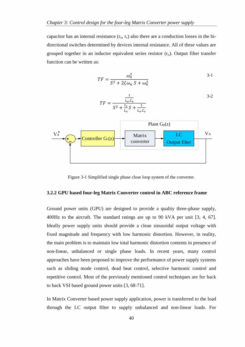
Chapter 3: Control design for the four-leg Matrix Converter power supply
40
capacitor has an internal resistance (ro, rc) also there are a conduction losses in the bi-
directional switches determined by devices internal resistance. All of these values are
grouped together in an inductor equivalent series resistor (ro). Output filter transfer
function can be written as:
3-1
3-2
LC
Output filterController Gc(z)
VAVA* Matrix
converter
Plant Gp(z)
Figure 3-1 Simplified single phase close loop system of the converter.
3.2.2 GPU based four-leg Matrix Converter control in ABC reference frame
Ground power units (GPU) are designed to provide a quality three-phase supply,
400Hz to the aircraft. The standard ratings are up to 90 kVA per unit [3, 4, 67].
Ideally power supply units should provide a clean sinusoidal output voltage with
fixed magnitude and frequency with low harmonic distortion. However, in reality,
the main problem is to maintain low total harmonic distortion contents in presence of
non-linear, unbalanced or single phase loads. In recent years, many control
approaches have been proposed to improve the performance of power supply systems
such as sliding mode control, dead beat control, selective harmonic control and
repetitive control. Most of the previously mentioned control techniques are for back
to back VSI based ground power units [3, 68-71].
In Matrix Converter based power supply application, power is transferred to the load
through the LC output filter to supply unbalanced and non-linear loads. For

Chapter 3: Control design for the four-leg Matrix Converter power supply
41
unbalanced load condition, the currents drawn from the converter are not balanced,
and due to the uneven voltage drop on the filter impedance zero sequence current
will flow in the system and this will cause a distortion in the output voltage. In
addition, when supplying non-linear loads, harmonic content of non-linear currents
causes distortion on the output voltages of the converter. According to that, the
output voltage needs to be controlled to guarantee a regulated stable, fixed voltage
and frequency with low harmonic distortion.
Output voltage control for a 400Hz output frequency requires a high bandwidth
controller. However, the controller bandwidth is limited due to the reduced ratio
between the converter switching frequency and the fundamental frequency [37], in
this case undesirable, periodic errors and distortion will exist in the output voltage
waveform [72]. A single voltage control loop operating in the ABC reference frame
as shown in Figure 3-1 is implemented in this work. The use of an internal current
loop is not attractive in this application due to bandwidth limitation of the digital
controller. If an internal current loop was included, it should be much faster than the
external voltage one. However, to be able to meet the very strict transient
specifications on the output voltage required for this application, the external voltage
loop needs to be as fast as possible. Therefore the implementation of a faster internal
current loop becomes impractical.

Chapter 3: Control design for the four-leg Matrix Converter power supply
42
3.2.3 Linear second order control design example for the four-leg Matrix
Converter
A simple case study is presented her as a design example for second order linear
controller for four-leg Matrix Converters. The design procedure of the second order
linear controller is demonstrated. System stability analysis and MATLAB simulation
results are also provided to validate the control design. The design of the second
order linear controller is carried-out using the root locus method. The pole zero
cancellation method is used to cancel the two undesired oscillatory poles of the
output filter and replace them with desired poles in order to suppress the resonant
peak as shown in Figure 3-2 and 3.5. The general form of the plant (LC filter) is :
( )( )
3-3
According to the system parameters in chapter 5, the plant parameters are, C=35µF,
L= 583µH and ro=0.2Ω. Consequently, the plant transfer function in S domain is:
3-4
And using 12.8KHz sampling frequency, the discrete plant transfer function using
zero-order-hold method is shown in equation 3-5:
3-5
Using direct controller design approach, the controller parameters can be found. As
can be seen in Figure 3-1, The open loop transfer function Gc(z) Gp(z) can described
in equation 3-6.
3-6
Where, Kp, A, B, C are the controller parameters that needs to be found. The second
order linear controller transfer function is given in equation 3-7.
Chapter 3: Control design for the four-leg Matrix Converter power supply
43
3-7
By solving the characteristics equation in the denominator of equation 3-7 the
controller coefficients can be found. The solution of this equation is a pair of poles,
which can be chosen to be on the real axes inside the unit circle.
3-8
The required controller bandwidth is around 150-200Hz to stabilize the system, and
by using MATLAB SISOtool as shown in Figure 3-2, the poles are found to be, Pc1=
- 0.5 and Pc2= 0.99, and the controller is shown in equation 3-9 with A=1, B=-0.495
and C=0.49. According to Matlab SISOtool, the gain value Kp can be chosen
between 0.05 and 0.4 that keep the close loop poles inside the unit circle. And in this
paper Kp is selected as 0.15.
3-9
The root locus of the open loop system is plotted in Figure 3-2, where the dominant
poles of the system has been compensated.
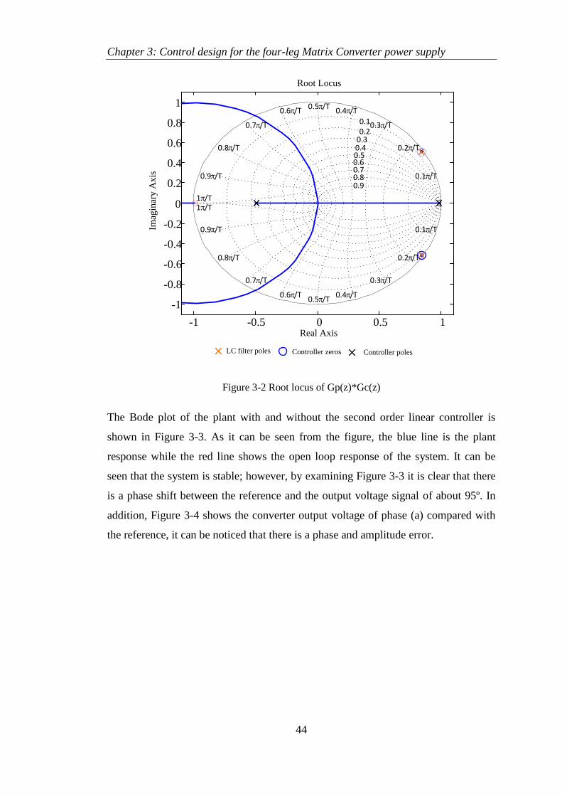
Chapter 3: Control design for the four-leg Matrix Converter power supply
44
-1 -0.5 0 0.5 1
-1
-0.8
-0.6
-0.4
-0.2
0
0.2
0.4
0.6
0.8
1
0.9/T
1/T
0.1/T
0.2/T
0.3/T
0.4/T0.5/T
0.6/T
0.7/T
0.8/T
0.9/T
1/T
0.10.2
0.30.40.50.60.70.80.9
0.1/T
0.2/T
0.3/T
0.4/T0.5/T
0.6/T
0.7/T
0.8/T
Root Locus
Real Axis
Imag
inar
y A
xis
LC filter poles Controller zeros Controller poles
Figure 3-2 Root locus of Gp(z)*Gc(z)
The Bode plot of the plant with and without the second order linear controller is
shown in Figure 3-3. As it can be seen from the figure, the blue line is the plant
response while the red line shows the open loop response of the system. It can be
seen that the system is stable; however, by examining Figure 3-3 it is clear that there
is a phase shift between the reference and the output voltage signal of about 95º. In
addition, Figure 3-4 shows the converter output voltage of phase (a) compared with
the reference, it can be noticed that there is a phase and amplitude error.
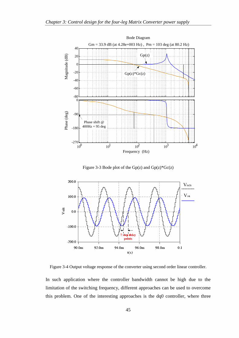
Chapter 3: Control design for the four-leg Matrix Converter power supply
45
-80
-60
-40
-20
0
20
40
Mag
nit
ud
e (d
B)
100
101
102
103
104
-270
-180
-90
0
Ph
ase
(deg
)
Bode Diagram
Gm = 33.9 dB (at 4.28e+003 Hz) , Pm = 103 deg (at 80.2 Hz)
Frequency (Hz)
Gp(z)*Gc(z)
Gp(z)
Phase shift @
400Hz = 95 deg
Figure 3-3 Bode plot of the Gp(z) and Gp(z)*Gc(z)
Figure 3-4 Output voltage response of the converter using second order linear controller.
In such application where the controller bandwidth cannot be high due to the
limitation of the switching frequency, different approaches can be used to overcome
this problem. One of the interesting approaches is the dq0 controller, where three
Chapter 3: Control design for the four-leg Matrix Converter power supply
46
controllers are needed for the d, q and 0 components. Another approach is to use
resonant controllers, where a high gain peak can be generated at the fundamental
frequency. To be able to control the harmonics, multiple resonant controllers need to
be adopted. To overcome this problem a repetitive controller can be used to regulate
the output voltage and achieve good tracking to reference signal.
3.3 Repetitive Control
Nowadays, many control systems required to handle repetitive tasks to track periodic
reference signals or reject a periodic disturbance. Along with more demanding
necessities for high precision tracking and steady state control quality and
performance, the use of conventional control approaches is not sufficient to meet the
often strict specifications and requirements. Hence, new control methods have been
investigated in literature to fulfil and meet these requirements. The concept of
repetitive control was originally developed by Inoue et al. in 1980 for a SISO plants
in continuous time domain to track a periodic repetitive signal with defined period T
[29], and was applied successfully to control proton synchrotron magnet power
supply in 1981 [29]. Based on the internal model principle (IMP) proposed by
Francis and Wonham in 1975, any periodic reference signal with known period T can
be tracked by including their generator in the stable closed loop[6]. In addition,
Repetitive Controller generates a high gain at the periodic signal fundamental
frequency and its integer multiples, therefore a periodic reference signal for example
can be tracked provided the close loop system is stable.
Repetitive controllers have been widely used in applications including PWM
inverters [30, 31],[32],[33], PWM rectifiers [34-36], Matrix Converter [4, 37, 38],
robotic manipulators [39], disk drive systems [40-42]. Repetitive controllers have
good steady state performance; however, its transient performance is poor, and that is
why the second order linear controller is used in conjunction with repetitive
controller to guarantee a good system performance in transients and steady state
conditions. It is worth mentioning that repetitive controller is not intended to stabilize
the plant, but to enhance an existing controller to remove periodic error signals.
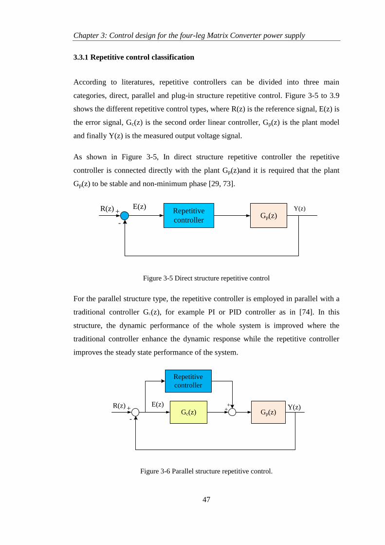
Chapter 3: Control design for the four-leg Matrix Converter power supply
47
3.3.1 Repetitive control classification
According to literatures, repetitive controllers can be divided into three main
categories, direct, parallel and plug-in structure repetitive control. Figure 3-5 to 3.9
shows the different repetitive control types, where R(z) is the reference signal, E(z) is
the error signal, Gc(z) is the second order linear controller, Gp(z) is the plant model
and finally Y(z) is the measured output voltage signal.
As shown in Figure 3-5, In direct structure repetitive controller the repetitive
controller is connected directly with the plant Gp(z)and it is required that the plant
Gp(z) to be stable and non-minimum phase [29, 73].
Gp(z)Y(z)R(z) +
-
E(z)Repetitive
controller
Figure 3-5 Direct structure repetitive control
For the parallel structure type, the repetitive controller is employed in parallel with a
traditional controller GC(z), for example PI or PID controller as in [74]. In this
structure, the dynamic performance of the whole system is improved where the
traditional controller enhance the dynamic response while the repetitive controller
improves the steady state performance of the system.
Repetitive
controller
Gp(z)Y(z)R(z) + +
+
-
E(z)Gc(z)
Figure 3-6 Parallel structure repetitive control.
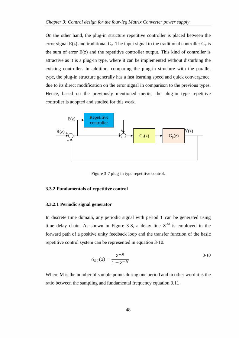
Chapter 3: Control design for the four-leg Matrix Converter power supply
48
On the other hand, the plug-in structure repetitive controller is placed between the
error signal E(z) and traditional Gc. The input signal to the traditional controller Gc is
the sum of error E(z) and the repetitive controller output. This kind of controller is
attractive as it is a plug-in type, where it can be implemented without disturbing the
existing controller. In addition, comparing the plug-in structure with the parallel
type, the plug-in structure generally has a fast learning speed and quick convergence,
due to its direct modification on the error signal in comparison to the previous types.
Hence, based on the previously mentioned merits, the plug-in type repetitive
controller is adopted and studied for this work.
Repetitive
controller
Gp(z)Y(z)R(z) + +
+
-Gc(z)
E(z)
Figure 3-7 plug-in type repetitive control.
3.3.2 Fundamentals of repetitive control
3.3.2.1 Periodic signal generator
In discrete time domain, any periodic signal with period T can be generated using
time delay chain. As shown in Figure 3-8, a delay line Z-M
is employed in the
forward path of a positive unity feedback loop and the transfer function of the basic
repetitive control system can be represented in equation 3-10.
3-10
Where M is the number of sample points during one period and in other word it is the
ratio between the sampling and fundamental frequency equation 3.11 .
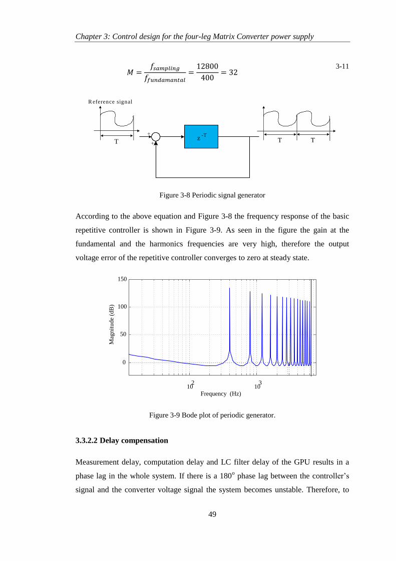
Chapter 3: Control design for the four-leg Matrix Converter power supply
49
3-11
Figure 3-8 Periodic signal generator
According to the above equation and Figure 3-8 the frequency response of the basic
repetitive controller is shown in Figure 3-9. As seen in the figure the gain at the
fundamental and the harmonics frequencies are very high, therefore the output
voltage error of the repetitive controller converges to zero at steady state.
Mag
nit
ude
(dB
)
Frequency (Hz)
0
50
100
150
102
103
Figure 3-9 Bode plot of periodic generator.
3.3.2.2 Delay compensation
Measurement delay, computation delay and LC filter delay of the GPU results in a
phase lag in the whole system. If there is a 180o phase lag between the controller’s
signal and the converter voltage signal the system becomes unstable. Therefore, to
+z
-T
R eference signal
+T TT
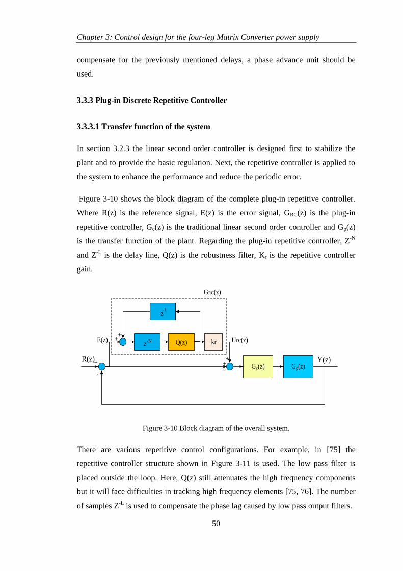
Chapter 3: Control design for the four-leg Matrix Converter power supply
50
compensate for the previously mentioned delays, a phase advance unit should be
used.
3.3.3 Plug-in Discrete Repetitive Controller
3.3.3.1 Transfer function of the system
In section 3.2.3 the linear second order controller is designed first to stabilize the
plant and to provide the basic regulation. Next, the repetitive controller is applied to
the system to enhance the performance and reduce the periodic error.
Figure 3-10 shows the block diagram of the complete plug-in repetitive controller.
Where R(z) is the reference signal, E(z) is the error signal, GRC(z) is the plug-in
repetitive controller, Gc(z) is the traditional linear second order controller and Gp(z)
is the transfer function of the plant. Regarding the plug-in repetitive controller, Z-N
and Z-L
is the delay line, Q(z) is the robustness filter, Kr is the repetitive controller
gain.
+z-N
+
Gp(z)Y(z)R(z)
Q(z) kr
+ ++
-Gc(z)
z-L
GRC(z)
Urc(z)E(z)
Figure 3-10 Block diagram of the overall system.
There are various repetitive control configurations. For example, in [75] the
repetitive controller structure shown in Figure 3-11 is used. The low pass filter is
placed outside the loop. Here, Q(z) still attenuates the high frequency components
but it will face difficulties in tracking high frequency elements [75, 76]. The number
of samples Z-L
is used to compensate the phase lag caused by low pass output filters.
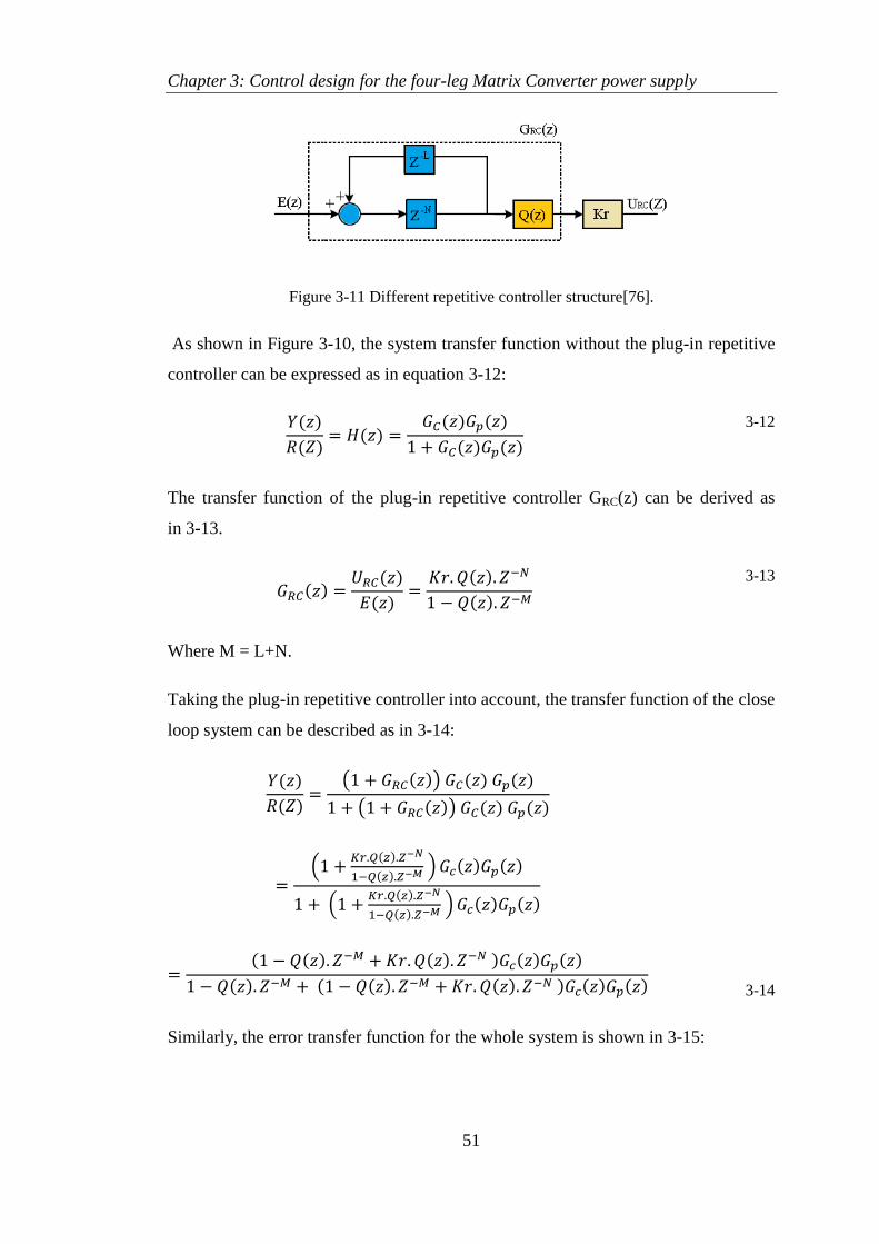
Chapter 3: Control design for the four-leg Matrix Converter power supply
51
Figure 3-11 Different repetitive controller structure[76].
As shown in Figure 3-10, the system transfer function without the plug-in repetitive
controller can be expressed as in equation 3-12:
3-12
The transfer function of the plug-in repetitive controller GRC(z) can be derived as
in 3-13.
Where M = L+N.
3-13
Taking the plug-in repetitive controller into account, the transfer function of the close
loop system can be described as in 3-14:
( )
( )
(
)
(
)
3-14
Similarly, the error transfer function for the whole system is shown in 3-15:
Chapter 3: Control design for the four-leg Matrix Converter power supply
52
( )
3-15
Now by substituting equation 3-13 into equation 3-15 the following equation can be
derived:
3-16
Based on equation 3-16, the equivalent system block diagram can be drawn as in
Figure 3-12 Equivalent system block diagram of equation 3-16
3.3.4 Stability Analysis
During the design procedure of the repetitive controller, the stability of the system
needs to be carefully analysed, since the open loop poles introduced by the periodic
signal generator are located on the stability boundary as shown in Figure 3-13. Any
inconsiderate design in the plug-in repetitive controller will affect the system
stability. Due to the complex form of the system transfer function, it is difficult to
utilize the traditional stability criteria for stability analysis, and in order to overcome
this problem, the small gain theorem is used to derive stability conditions for
repetitive control systems [77-79].
Chapter 3: Control design for the four-leg Matrix Converter power supply
53
Figure 3-13 Pole zero map of the system in Figure 3-8
3.3.4.1 Small Gain Theorem
The concept of the small gain theorem was initially suggested by Zames in 1966.
Regarding a typical negative feedback control system shown in Figure 3-14, the
small gain theorem states that the closed-loop system is bounded input, bounded
output stable if both R(z) and D(z) are bounded and the loop gain |GC(z)GP(z)| is less
than unity [80].
G p(z)
R (z)+ +
+
-
E(z)
G c(z)
Y (z)
D (z)
Figure 3-14 Negative feedback system
-1 -0.8 -0.6 -0.4 -0.2 0 0.2 0.4 0.6 0.8 1
-1
-0.8
-0.6
-0.4
-0.2
0
0.2
0.4
0.6
0.8
1
Pole-Zero M ap
R eal A xis
Ima
gin
ary
Ax
is
Chapter 3: Control design for the four-leg Matrix Converter power supply
54
3.3.4.2 Stability Conditions
To simplify the analysis, the equivalent block diagram shown in Figure 3-12 to
analyse the stability conditions of the plug-in repetitive control system based on
equation 3-16. The block diagram contains three main blocks A, B and C, so, for the
system to be stable theses three blocks needs to be stable. The first block, block A
consists of the robustness filter Q(z) and the delay line z-N
. Usually, Q(z) is chosen to
be a low pass filter, which passes the low and medium frequencies with unity gain
and attenuates high order frequencies. On the other hand, Q(z) can be a close to unity
constant, e.g. 0.95. Under these two conditions, the first block is always stable, and
the selection of Q(z) will be discussed later. The second block, block B has transfer
function with a denominator of 1+GC(z)GP(z), which is the characteristic equation of
the closed loop feedback system without the repetitive controller and this is stable as
discussed earlier. The last block, which is block C has a complex transfer function in
the feedback loop, and the small gain theorem, can be used to simplify the analysis.
According to the small gain theorem, block C will be stable if the entire loop gain is
smaller than unity when the frequency changes from zero to the Nyquest frequency.
‖( )‖
[ ]
Where
3-17
S(z) is plotted with MATLAB as shown in Figure 3-15. In the figure, the locus of
S(z) is always in the unity circle, which satisfy the stability condition. Hence, the
system is stable.
Chapter 3: Control design for the four-leg Matrix Converter power supply
55
-1 -0.8 -0.6 -0.4 -0.2 0 0.2 0.4 0.6 0.8 1-1
-0.8
-0.6
-0.4
-0.2
0
0.2
0.4
0.6
0.8
1Nyquist Diagram
Real Axis
Imag
inar
y A
xis
Figure 3-15 The Nyquist diagram of S(z).
3.3.5 Design of the robustness filter Q(z)
In the discrete periodic signal generator given in Figure 3-8, a perfect reference
tracking or/and complete disturbance rejecting can be achieved in steady state.
However, the open loop poles of the repetitive controller are on the stability
boundary, and the overall stability of the system is sensitive to the un-modelled
dynamics as shown in Figure 3-13. In order to enhance the system stability,
robustness filter Q(z) is employed in the system as shown in Figure 3-10. This filter
can be as a constant or a low pass filter. The simplest choice of Q(z) is a close to
unity constant typically 0.95 [81], as it can be implemented and adjusted easily in
digital control system. On the other hand, the low pass filter is more complicated
than a constant, but the low pass filter holds the system with larger stability margin
than a constant. Because of that, Q(z) is set as a notch zero phase shift filter in this
work, and Q(z)=(z+2+z-1)/4. From the bode plot of Q(z) in Figure 3-16, it can be
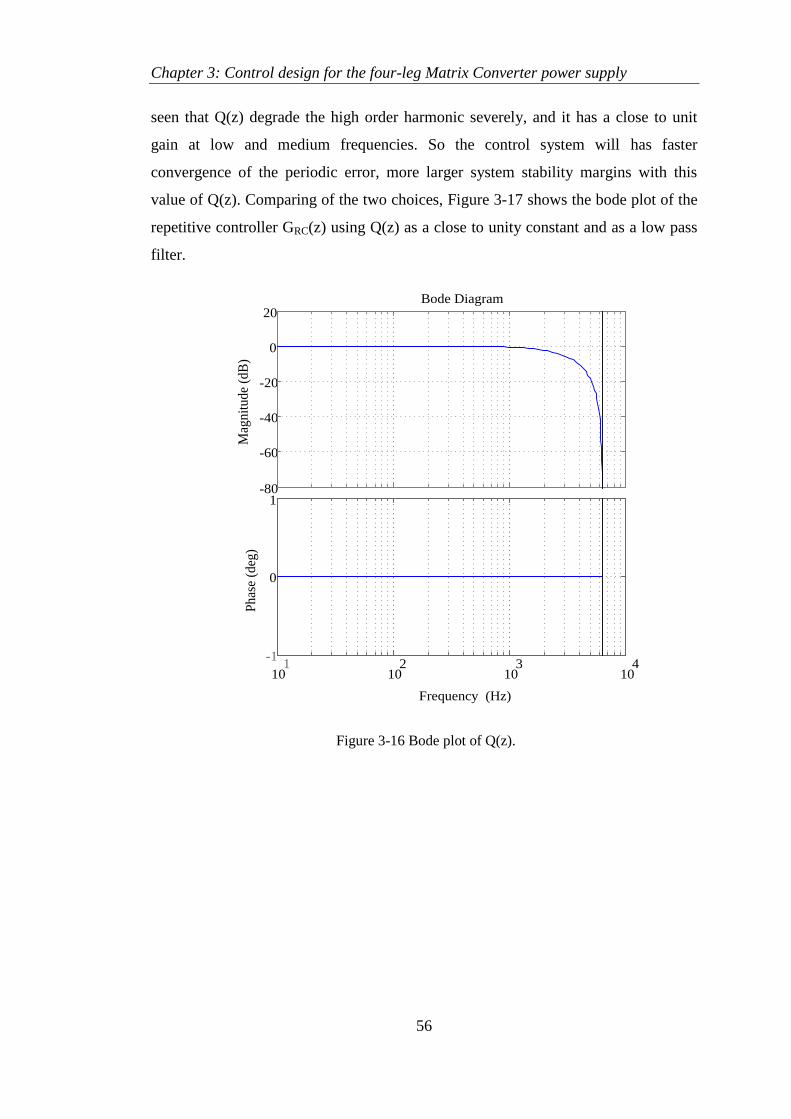
Chapter 3: Control design for the four-leg Matrix Converter power supply
56
seen that Q(z) degrade the high order harmonic severely, and it has a close to unit
gain at low and medium frequencies. So the control system will has faster
convergence of the periodic error, more larger system stability margins with this
value of Q(z). Comparing of the two choices, Figure 3-17 shows the bode plot of the
repetitive controller GRC(z) using Q(z) as a close to unity constant and as a low pass
filter.
-80
-60
-40
-20
0
20
Mag
nit
ude
(dB
)
101
102
103
104
-1
0
1
Phas
e (d
eg)
Bode Diagram
Frequency (Hz)
Figure 3-16 Bode plot of Q(z).
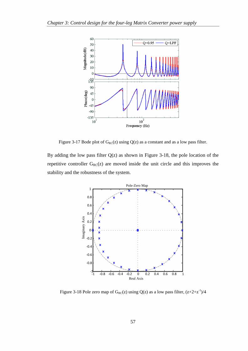
Chapter 3: Control design for the four-leg Matrix Converter power supply
57
Figure 3-17 Bode plot of GRC(z) using Q(z) as a constant and as a low pass filter.
By adding the low pass filter Q(z) as shown in Figure 3-18, the pole location of the
repetitive controller GRC(z) are moved inside the unit circle and this improves the
stability and the robustness of the system.
-1 -0.8 -0.6 -0.4 -0.2 0 0.2 0.4 0.6 0.8 1-1
-0.8
-0.6
-0.4
-0.2
0
0.2
0.4
0.6
0.8
1Pole-Zero Map
Real Axis
Imag
inar
y A
xis
Figure 3-18 Pole zero map of GRC(z) using Q(z) as a low pass filter, (z+2+z-1
)/4

Chapter 3: Control design for the four-leg Matrix Converter power supply
58
3.3.6 Time advance unit (ZL) design
The value of time advance unit ZL is added to the system to compensate for the phase
delay introduced by the plant Gp(z) and the controller Gc(z). When an input voltage
is applied to the system shown in Figure 3-14, that consists of plant and the second
order controller only, the output voltage will be reduced and phase shifted with
respect to the input voltage as shown in Figure 3-19 and Figure 3-20. According to
these figures, at 400Hz frequency there is a phase shift in the output voltage of 95o
with respect to the reference. The stability of the repetitive controller has been shown
to greatly improve if a phase lead compensator of L samples is added to the repetitive
controller to compensate for this delay. And this will increase the system phase
margin. The value of L can be calculated from Figure 3-19 and Figure 3-20. It can be
seen that using 12800Hz switching frequency and 400Hz output frequency, the
voltage waveform cycle consists of 32 points, and a phase shift of 95o is equivalent
to 8.4 steps which is rounded to 8 delay samples according to equation 3-18:
3-18
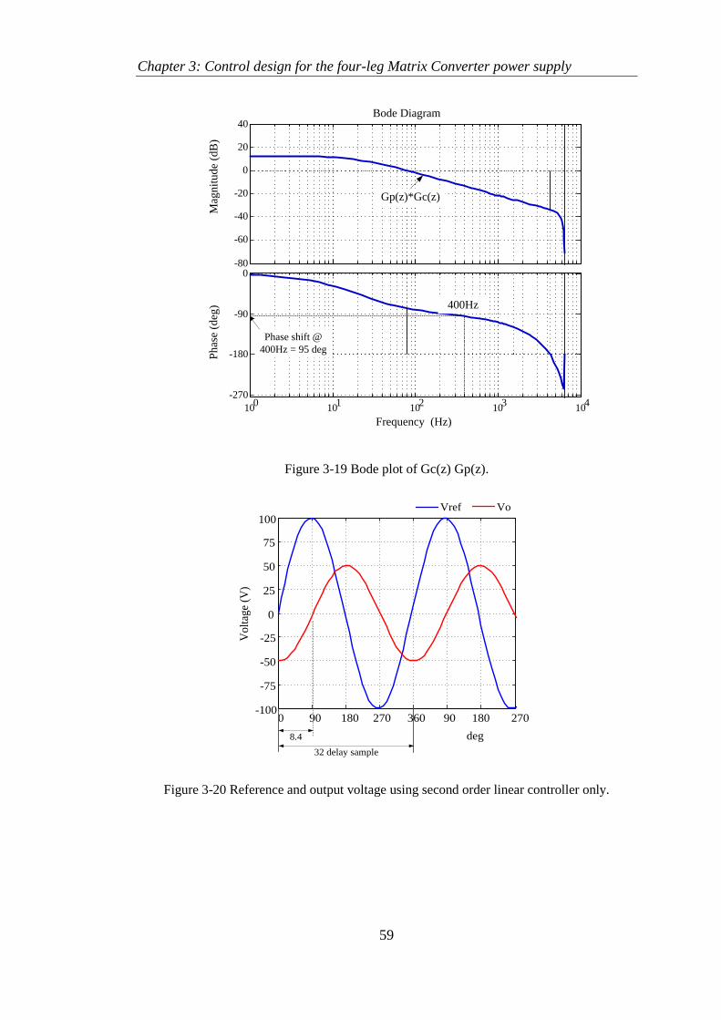
Chapter 3: Control design for the four-leg Matrix Converter power supply
59
-80
-60
-40
-20
0
20
40
Mag
nit
ude
(dB
)
100
101
102
103
104
-270
-180
-90
0
Phas
e (d
eg)
Bode Diagram
Frequency (Hz)
Gp(z)*Gc(z)
Phase shift @
400Hz = 95 deg
400Hz
Figure 3-19 Bode plot of Gc(z) Gp(z).
0 90 180 270 360 90 180 270-100
-75
-50
-25
0
25
50
75
100
deg
Vo
ltag
e (V
)
8.4
32 delay sample
Vref Vo
Figure 3-20 Reference and output voltage using second order linear controller only.

Chapter 3: Control design for the four-leg Matrix Converter power supply
60
3.3.7 Design example of four-leg Matrix Converter using second order linear
controller and plug-in repetitive controller
In order to verify the effectiveness of the proposed design theory, a simple case study
is analysed as design example. The design procedure and parameter selection of the
repetitive controller are shown. System stability analysis and MATLAB simulation
results are also provided to validate the control design.
3.3.7.1 Repetitive Control Design
A plug-in type repetitive controller is to improve the performance of system.
Figure 3-22 shows the complete plug-in repetitive control system, where GRC(z) is
the plug-in repetitive controller; kr is the repetitive gain; z-N
is the delay line; Q(z) is
the robustness filter and z-N
is the time advance unit. All of the previously mentioned
parameters need to be found.
3.3.7.1.1 Periodic Signal Generator
The periodic signal model needs to be included in the stable closed loop control
system in order to ensure perfect reference tracking. And this can be achieved in
discrete time domain by employing the delay term z-M
in the forward path of a
positive unity feedback loop as discussed in section 3.3.2.1. The value of M can be
determined by solving equation 3-11
3.3.7.1.2 Time advance unit L
As can be seen in Figure 3-19 and Figure 3-20 the value of time advance unit L can
be found. By carefully examining the figures, we can see that the output voltage of
the converter lags the reference signal y 95o. According to equation 3-18, the value
of L is equivalent to 8 points.
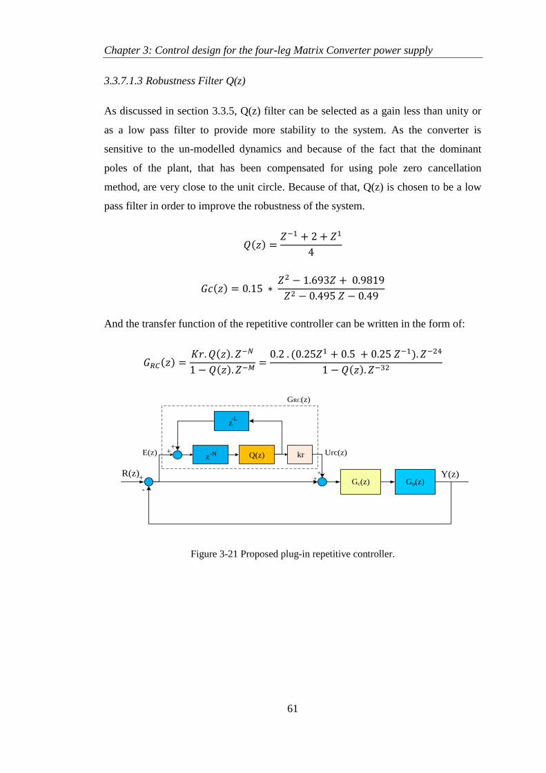
Chapter 3: Control design for the four-leg Matrix Converter power supply
61
3.3.7.1.3 Robustness Filter Q(z)
As discussed in section 3.3.5, Q(z) filter can be selected as a gain less than unity or
as a low pass filter to provide more stability to the system. As the converter is
sensitive to the un-modelled dynamics and because of the fact that the dominant
poles of the plant, that has been compensated for using pole zero cancellation
method, are very close to the unit circle. Because of that, Q(z) is chosen to be a low
pass filter in order to improve the robustness of the system.
And the transfer function of the repetitive controller can be written in the form of:
+z-N
+
Gp(z)Y(z)R(z)
Q(z) kr
+ ++
-Gc(z)
z-L
GRC(z)
Urc(z)E(z)
Figure 3-21 Proposed plug-in repetitive controller.
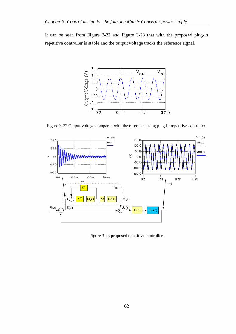
Chapter 3: Control design for the four-leg Matrix Converter power supply
62
It can be seen from Figure 3-22 and Figure 3-23 that with the proposed plug-in
repetitive controller is stable and the output voltage tracks the reference signal.
Figure 3-22 Output voltage compared with the reference using plug-in repetitive controller.
Figure 3-23 proposed repetitive controller.

Chapter 3: Control design for the four-leg Matrix Converter power supply
63
3.4 Summary
This chapter has discussed the modeling, design and analysis of the control system
for the four-leg Matrix Converter for power supply applications. MATLAB/Simulink
package have been used to model, design and simulate the power supply system. In
this chapter, a second order controller is used in conjunction with a plug-in repetitive
controller to control the converter. The second order controller used to improve
system dynamics in transient conditions, while the repetitive controller serves to
eliminate any periodic error and improve the steady state response of the system. In
addition, the stability of the proposed controller has also been discussed in the
chapter and a good stability margin has been found.
In the following chapters, the simulation and the experimental results will be
presented to test the effectiveness of the proposed controller to control the four-leg
Matrix Converter for different load conditions.
Chapter 4: Power converter simulation
64
Chapter 4 Power converter simulation
4.1 Introduction
Simulation is the imitation of a real system or process through a series of equations
that represent the relations between the input and the output. The act of simulating a
system generally entails considering a limited number of key characteristics and
behaviours within the physical system of interest, which is otherwise infinitely
complex and detailed.
Power converter simulation allows us to examine the behaviour of the system under
different scenarios. Power converter simulation can provide a safe and relatively
cheaper test bed to operate, evaluate and optimize the performance of the system
before realizing it in the physical world [82].
This chapter describing the modelling and simulation of the GPU system shown in
Figure 4-1 and the associated controller for a range of load conditions. The purpose
of the simulation is to verify the effectiveness of the proposed controller and the use
of four-leg Matrix Converter as GPU for aircraft applications. Modelling and
simulation of the GPU system is required before the real implementation to
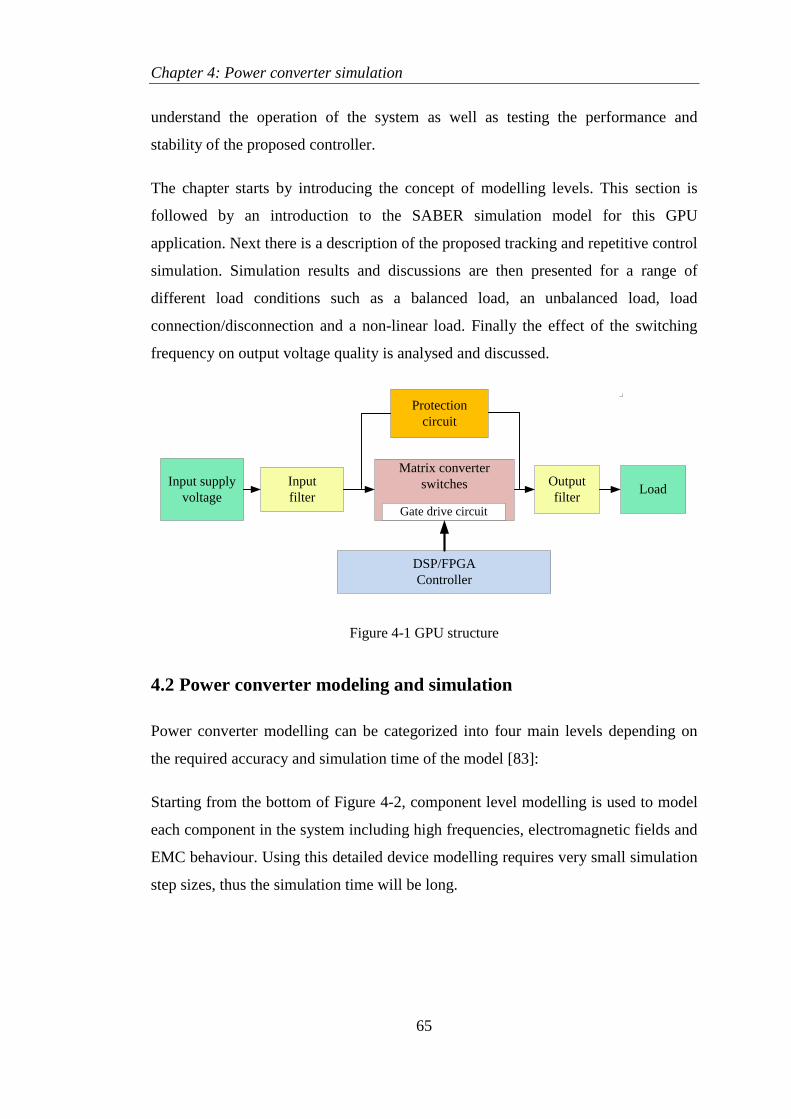
Chapter 4: Power converter simulation
65
understand the operation of the system as well as testing the performance and
stability of the proposed controller.
The chapter starts by introducing the concept of modelling levels. This section is
followed by an introduction to the SABER simulation model for this GPU
application. Next there is a description of the proposed tracking and repetitive control
simulation. Simulation results and discussions are then presented for a range of
different load conditions such as a balanced load, an unbalanced load, load
connection/disconnection and a non-linear load. Finally the effect of the switching
frequency on output voltage quality is analysed and discussed.
Matrix converter
switchesInput
filter
Input supply
voltage
Output
filter
Protection
circuit
Gate drive circuit
DSP/FPGA
Controller
Load
Figure 4-1 GPU structure
4.2 Power converter modeling and simulation
Power converter modelling can be categorized into four main levels depending on
the required accuracy and simulation time of the model [83]:
Starting from the bottom of Figure 4-2, component level modelling is used to model
each component in the system including high frequencies, electromagnetic fields and
EMC behaviour. Using this detailed device modelling requires very small simulation
step sizes, thus the simulation time will be long.
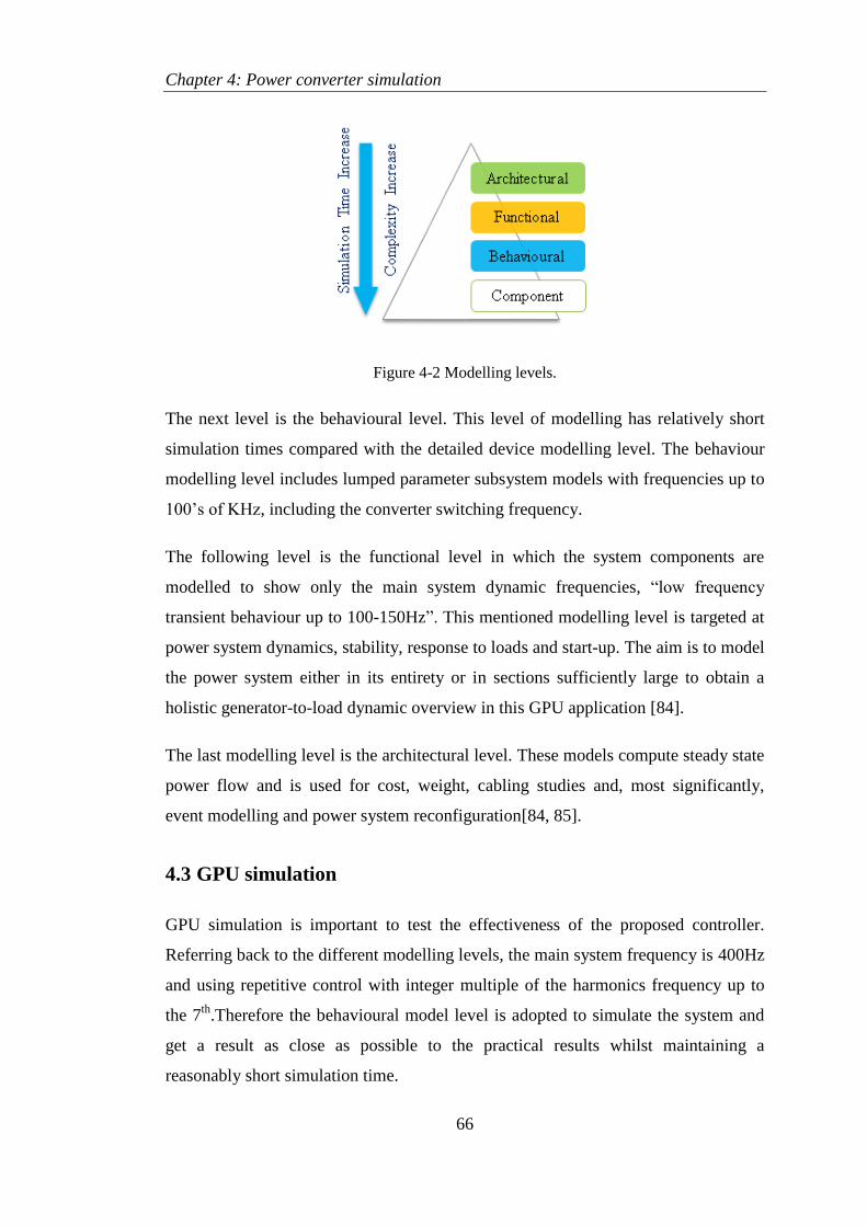
Chapter 4: Power converter simulation
66
Figure 4-2 Modelling levels.
The next level is the behavioural level. This level of modelling has relatively short
simulation times compared with the detailed device modelling level. The behaviour
modelling level includes lumped parameter subsystem models with frequencies up to
100’s of KHz, including the converter switching frequency.
The following level is the functional level in which the system components are
modelled to show only the main system dynamic frequencies, “low frequency
transient behaviour up to 100-150Hz”. This mentioned modelling level is targeted at
power system dynamics, stability, response to loads and start-up. The aim is to model
the power system either in its entirety or in sections sufficiently large to obtain a
holistic generator-to-load dynamic overview in this GPU application [84].
The last modelling level is the architectural level. These models compute steady state
power flow and is used for cost, weight, cabling studies and, most significantly,
event modelling and power system reconfiguration[84, 85].
4.3 GPU simulation
GPU simulation is important to test the effectiveness of the proposed controller.
Referring back to the different modelling levels, the main system frequency is 400Hz
and using repetitive control with integer multiple of the harmonics frequency up to
the 7th
.Therefore the behavioural model level is adopted to simulate the system and
get a result as close as possible to the practical results whilst maintaining a
reasonably short simulation time.

Chapter 4: Power converter simulation
67
Saber is a powerful simulation package which can be used to model different
physical systems. The Saber simulation package has been selected to simulate the
GPU based Matrix Converter in this work.
Using Saber, varying degrees of model complexity can be achieved by combining the
predefined parts in the device model library with the functional description blocks
written using Saber’s internal scripting language, MAST modelling language. The
MAST modelling language is a Hardware Description Language (HDL) from
Synopsys, released in 1986. MAST is an advanced modelling language available for
analogue, mixed-signal and mixed-technology applications, it gives the programmer
a way to describe and model both analogue and digital circuits.
5.1.1. Saber simulation of four-leg Matrix Converter
Schematic of the four-leg Matrix Converter model is shown in Figure 4-3. The
converter system consists of 5 main parts that needs to be modelled. These parts are:
Input power supply.
Input filter.
Bidirectional switches.
Output filter and load.
Modulation and control.
The subsystems such as input power supply, input filter, bidirectional switches,
output filter and three phase load are modelled using the existing components in
Saber standard library. The input voltages must be measured at each cycle period, in
order to correct the duty cycles necessary to generate balanced and sinusoidal output
voltages. It is possible to increase the system stability by filtering the measured input
voltage and using the filtered signals for duty cycle calculations of Matrix Converter
switching configuration [86].
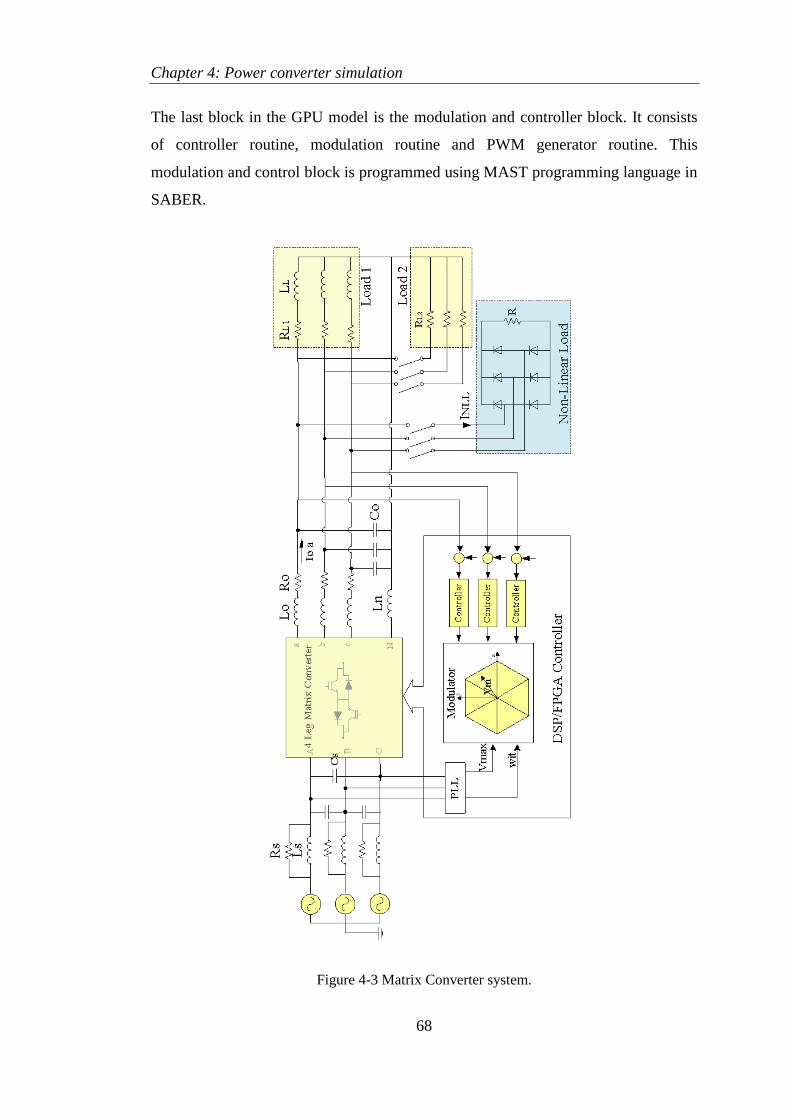
Chapter 4: Power converter simulation
68
The last block in the GPU model is the modulation and controller block. It consists
of controller routine, modulation routine and PWM generator routine. This
modulation and control block is programmed using MAST programming language in
SABER.
Figure 4-3 Matrix Converter system.

Chapter 4: Power converter simulation
69
4.3.1 Simulation flowchart
As shown in Figure 4-4, the MAST code consists of three main subroutines executed
in series theses routine are: control routine, Modulation routine, and PWM waveform
generator routine. First, the control routine starts by measuring the three phase output
voltages (Vo) and compare them with the reference and calculate the command signal
that is fed into the modulator. Then, in the modulation stage, both the controller
output and the three phase input voltage signals will be processed using Venturini
modulation algorithm to calculate the required duty cycles. After that, the calculated
duty cycles passed to the PWM generator routine to generate the required pulses to
switch the bidirectional switches ON/OFF using schedule events function in the
MAST language.
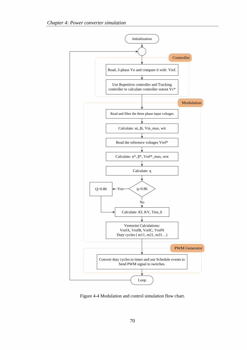
Chapter 4: Power converter simulation
70
Controller
Modulation
PWM Generator
Read and filter the three phase input voltages
Initialization
Read the reference voltages Vref*
q>0.86Yes
Calculate: KI, KV, Teta_h
No
Ventorini Calculations:
VrefA, VrefB, VrefC, VrefN
Duty cycles ( m11, m21, m31…)
Loop
Calculate: αi, βi, Vin_max, wit
Calculate: α*, β*, Vref*_max, wot
Calculate: q
Convert duty cycles to times and use Schedule events to
Send PWM signal to switches.
Q=0.86
Read..3-phase Vo and compare it with Vref.
Use Repetitive controller and Tracking
controller to calculate controller outout Vc*
Figure 4-4 Modulation and control simulation flow chart.

Chapter 4: Power converter simulation
71
4.3.2 System parameters
The main system parameters are shown below as follows:
Input supply voltage: three phase supply, 50Hz, 294Vrms (line to line).
Output power: 7.5KW.
Output voltage: Three phase, 115 Vrms (line to neutral)
Output frequency: 400 Hz.
Switching frequency: 12800Hz
Output filter: Lo=583uH, Co=35uF.
Input filter: Ls=600uH, Cs=2uF
The above listed parameters have been selected to test the GPU based Matrix
Converter. The converter output voltage and frequency is set to 115V and 400Hz
respectively. In practical testing a total output power of 4.5KVA was chosen
according to the available test facilities.
The selection of the switching frequency is a trade-off between efficiency,
component size and transient response. Higher switching frequency is desirable and
it will reduce the inductors and capacitors size and increase the transient response of
the voltage regulation by having larger control bandwidth. However, converter
efficiency will be lower due to increased conduction and switching losses. A12800
Hz switching frequency is selected, although this switching frequency can be
increased up to 20kHz. However, huge calculations associated with the repetitive
control and the modulation algorithms are required. The maximum time required to
run all the calculations is around 77uS, and according to that, a 12.8 kHz is selected
which give 78.125us.
4.3.3 Matrix Converter operation under balanced load
The simulation results of the converter connected to a balanced load for steady state
operation are shown in Figure 4-5 to Figure 4.13.
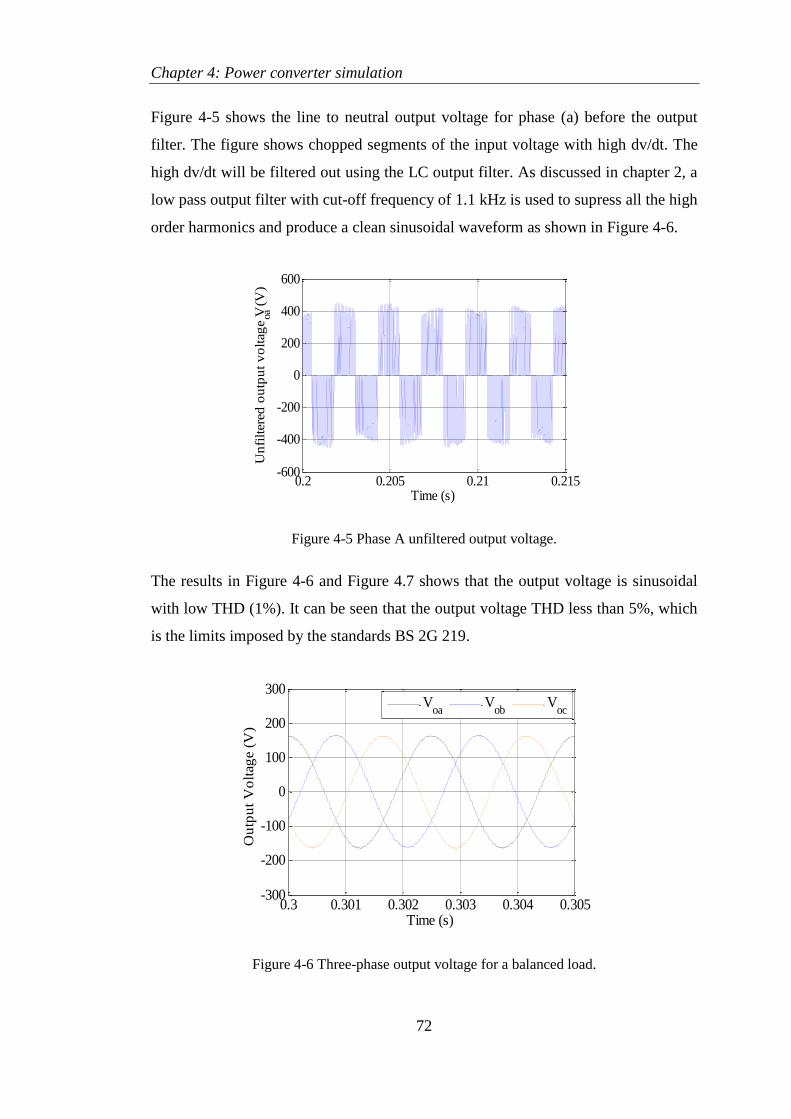
Chapter 4: Power converter simulation
72
Figure 4-5 shows the line to neutral output voltage for phase (a) before the output
filter. The figure shows chopped segments of the input voltage with high dv/dt. The
high dv/dt will be filtered out using the LC output filter. As discussed in chapter 2, a
low pass output filter with cut-off frequency of 1.1 kHz is used to supress all the high
order harmonics and produce a clean sinusoidal waveform as shown in Figure 4-6.
Figure 4-5 Phase A unfiltered output voltage.
The results in Figure 4-6 and Figure 4.7 shows that the output voltage is sinusoidal
with low THD (1%). It can be seen that the output voltage THD less than 5%, which
is the limits imposed by the standards BS 2G 219.
Figure 4-6 Three-phase output voltage for a balanced load.
0.2 0.205 0.21 0.215-600
-400
-200
0
200
400
600
Time (s)
Un
filt
ered
ou
tpu
t v
olt
age
V
oa (
V)
0.3 0.301 0.302 0.303 0.304 0.305-300
-200
-100
0
100
200
300
Time (s)
Ou
tpu
t V
olt
age
(V)
Voa
Vob
Voc
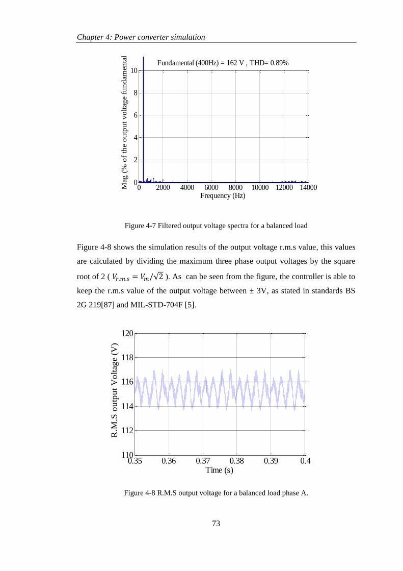
Chapter 4: Power converter simulation
73
Figure 4-7 Filtered output voltage spectra for a balanced load
Figure 4-8 shows the simulation results of the output voltage r.m.s value, this values
are calculated by dividing the maximum three phase output voltages by the square
root of 2 ( √ ). As can be seen from the figure, the controller is able to
keep the r.m.s value of the output voltage between ± 3V, as stated in standards BS
2G 219[87] and MIL-STD-704F [5].
Figure 4-8 R.M.S output voltage for a balanced load phase A.
0 2000 4000 6000 8000 10000 12000 140000
2
4
6
8
10
Frequency (Hz)
Fundamental (400Hz) = 162 V , THD= 0.89%
Mag
(%
of
the
ou
tpu
t v
olt
age
fun
dam
enta
l )
0.35 0.36 0.37 0.38 0.39 0.4110
112
114
116
118
120
Time (s)
R.M
.S o
utp
ut
Vo
ltag
e (V
)
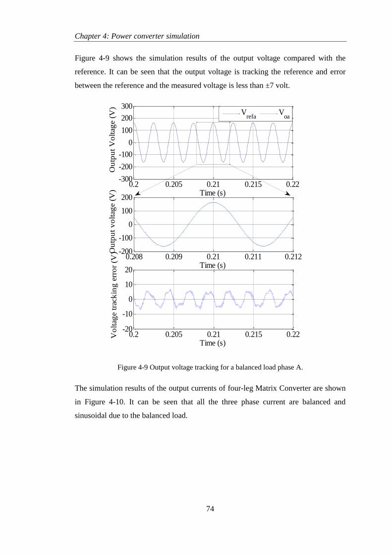
Chapter 4: Power converter simulation
74
Figure 4-9 shows the simulation results of the output voltage compared with the
reference. It can be seen that the output voltage is tracking the reference and error
between the reference and the measured voltage is less than ±7 volt.
Figure 4-9 Output voltage tracking for a balanced load phase A.
The simulation results of the output currents of four-leg Matrix Converter are shown
in Figure 4-10. It can be seen that all the three phase current are balanced and
sinusoidal due to the balanced load.
0.2 0.205 0.21 0.215 0.22-300
-200
-100
0
100
200
300
Time (s)
Ou
tpu
t V
olt
age
(V)
V
refaV
oa
0.208 0.209 0.21 0.211 0.212-200
-100
0
100
200
Time (s)
Ou
tpu
t v
olt
age
(V)
0.2 0.205 0.21 0.215 0.22-20
-10
0
10
20
Time (s)
Vo
ltag
e tr
ack
ing
err
or
(V)
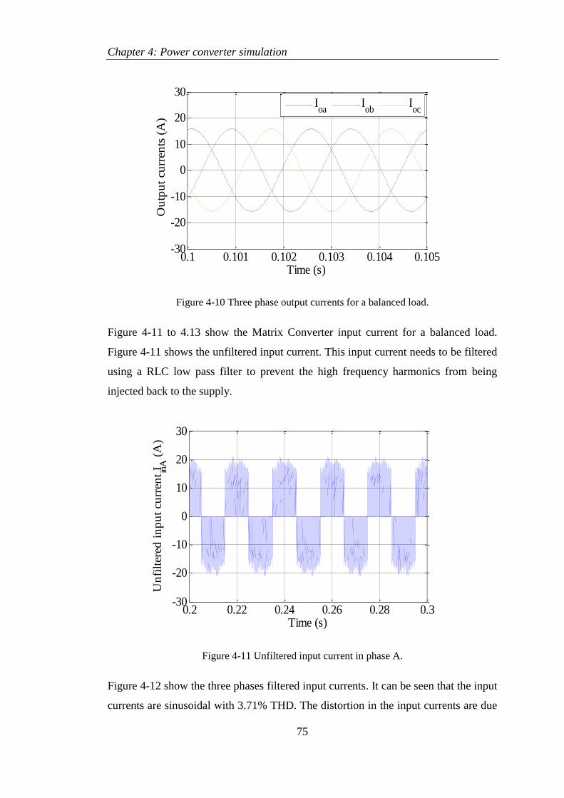
Chapter 4: Power converter simulation
75
Figure 4-10 Three phase output currents for a balanced load.
Figure 4-11 to 4.13 show the Matrix Converter input current for a balanced load.
Figure 4-11 shows the unfiltered input current. This input current needs to be filtered
using a RLC low pass filter to prevent the high frequency harmonics from being
injected back to the supply.
Figure 4-11 Unfiltered input current in phase A.
Figure 4-12 show the three phases filtered input currents. It can be seen that the input
currents are sinusoidal with 3.71% THD. The distortion in the input currents are due
0.1 0.101 0.102 0.103 0.104 0.105-30
-20
-10
0
10
20
30
Time (s)
Ou
tpu
t cu
rren
ts (
A)
Ioa
Iob
Ioc
0.2 0.22 0.24 0.26 0.28 0.3-30
-20
-10
0
10
20
30
Time (s)
Un
filt
ered
in
pu
t cu
rren
t I
in
A (
A)
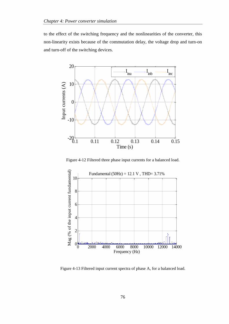
Chapter 4: Power converter simulation
76
to the effect of the switching frequency and the nonlinearities of the converter, this
non-linearity exists because of the commutation delay, the voltage drop and turn-on
and turn-off of the switching devices.
Figure 4-12 Filtered three phase input currents for a balanced load.
Figure 4-13 Filtered input current spectra of phase A, for a balanced load.
0.1 0.11 0.12 0.13 0.14 0.15-20
-10
0
10
20
Time (s)
Inp
ut
curr
ents
(A
)
Iina
Iinb
Iinc
0 2000 4000 6000 8000 10000 12000 140000
2
4
6
8
10
Frequency (Hz)
Fundamental (50Hz) = 12.1 V , THD= 3.71%
Mag
(%
of
the
inp
ut
curr
ent
fun
dam
enta
l)
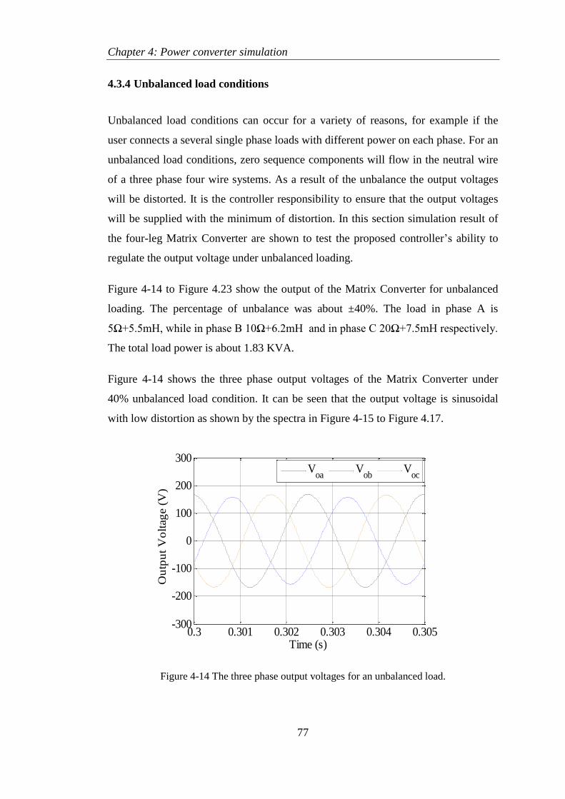
Chapter 4: Power converter simulation
77
4.3.4 Unbalanced load conditions
Unbalanced load conditions can occur for a variety of reasons, for example if the
user connects a several single phase loads with different power on each phase. For an
unbalanced load conditions, zero sequence components will flow in the neutral wire
of a three phase four wire systems. As a result of the unbalance the output voltages
will be distorted. It is the controller responsibility to ensure that the output voltages
will be supplied with the minimum of distortion. In this section simulation result of
the four-leg Matrix Converter are shown to test the proposed controller’s ability to
regulate the output voltage under unbalanced loading.
Figure 4-14 to Figure 4.23 show the output of the Matrix Converter for unbalanced
loading. The percentage of unbalance was about ±40%. The load in phase A is
5Ω+5.5mH, while in phase B 10Ω+6.2mH and in phase C 20Ω+7.5mH respectively.
The total load power is about 1.83 KVA.
Figure 4-14 shows the three phase output voltages of the Matrix Converter under
40% unbalanced load condition. It can be seen that the output voltage is sinusoidal
with low distortion as shown by the spectra in Figure 4-15 to Figure 4.17.
Figure 4-14 The three phase output voltages for an unbalanced load.
0.3 0.301 0.302 0.303 0.304 0.305-300
-200
-100
0
100
200
300
Time (s)
Ou
tpu
t V
olt
age
(V)
Voa
Vob
Voc
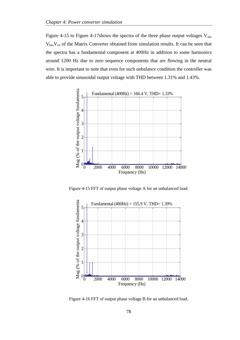
Chapter 4: Power converter simulation
78
Figure 4-15 to Figure 4-17shows the spectra of the three phase output voltages Van,
Vbn,Vcn of the Matrix Converter obtained from simulation results. It can be seen that
the spectra has a fundamental component at 400Hz in addition to some harmonics
around 1200 Hz due to zero sequence components that are flowing in the neutral
wire. It is important to note that even for such unbalance condition the controller was
able to provide sinusoidal output voltage with THD between 1.31% and 1.43%.
Figure 4-15 FFT of output phase voltage A for an unbalanced load.
Figure 4-16 FFT of output phase voltage B for an unbalanced load.
0 2000 4000 6000 8000 10000 12000 140000
1
2
3
4
5
Frequency (Hz)
Fundamental (400Hz) = 166.4 V, THD= 1.33%
Mag
(%
of
the
ou
tpu
t v
olt
age
fun
dam
enta
l)
0 2000 4000 6000 8000 10000 12000 140000
1
2
3
4
5
Frequency (Hz)
Fundamental (400Hz) = 155.9 V, THD= 1.39%
Mag
(%
of
the
ou
tpu
t v
olt
age
fun
dam
enta
l)
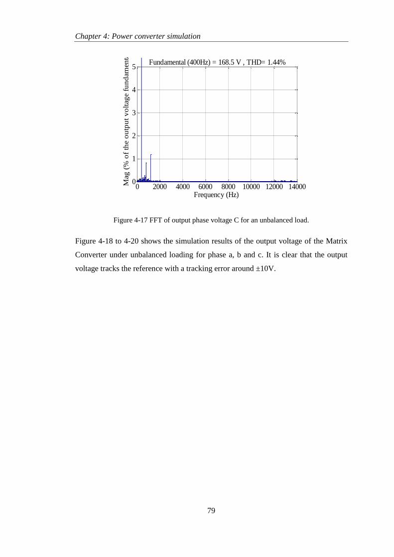
Chapter 4: Power converter simulation
79
Figure 4-17 FFT of output phase voltage C for an unbalanced load.
Figure 4-18 to 4-20 shows the simulation results of the output voltage of the Matrix
Converter under unbalanced loading for phase a, b and c. It is clear that the output
voltage tracks the reference with a tracking error around ±10V.
0 2000 4000 6000 8000 10000 12000 140000
1
2
3
4
5
Frequency (Hz)
Fundamental (400Hz) = 168.5 V , THD= 1.44%
Mag
(%
of
the
ou
tpu
t v
olt
age
fun
dam
enta
l)
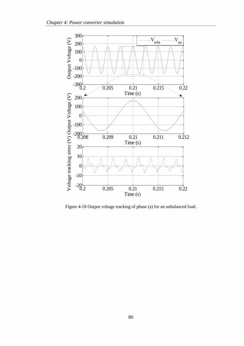
Chapter 4: Power converter simulation
80
Figure 4-18 Output voltage tracking of phase (a) for an unbalanced load.
0.2 0.205 0.21 0.215 0.22-300
-200
-100
0
100
200
300
Time (s)
Ou
tpu
t V
olt
age
(V)
Vrefa
Voa
0.2 0.205 0.21 0.215 0.22-20
-10
0
10
20
Time (s)
Vo
ltag
e tr
ack
ing
err
or
(V) 0.208 0.209 0.21 0.211 0.212
-200
-100
0
100
200
Time (s)
Ou
tpu
t V
olt
age
(V)
Vrefa
Voa
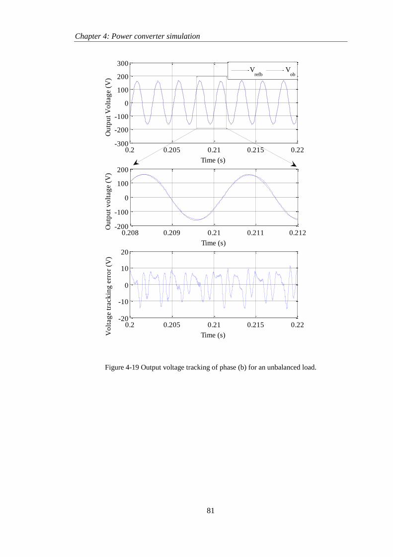
Chapter 4: Power converter simulation
81
Figure 4-19 Output voltage tracking of phase (b) for an unbalanced load.
0.2 0.205 0.21 0.215 0.22-300
-200
-100
0
100
200
300
Time (s)
Ou
tpu
t V
olt
ag
e (
V)
Vrefb
Vob
0.208 0.209 0.21 0.211 0.212-200
-100
0
100
200
Time (s)
Ou
tpu
t v
olt
ag
e (
V)
0.2 0.205 0.21 0.215 0.22-20
-10
0
10
20
Time (s)Vo
ltag
e t
rack
ing
err
or
(V)
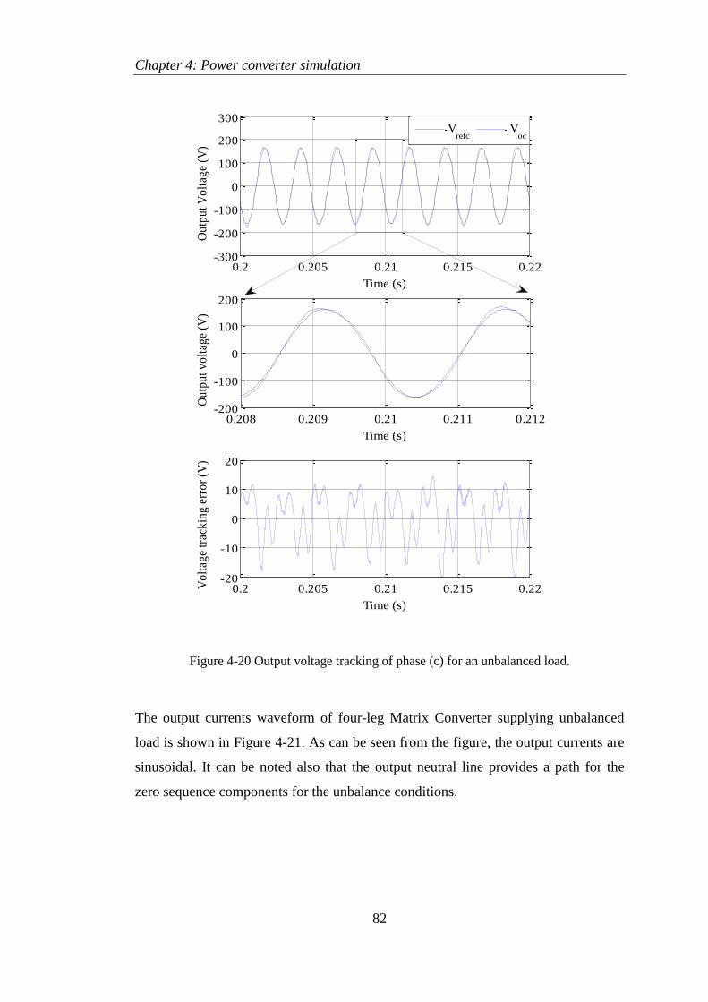
Chapter 4: Power converter simulation
82
Figure 4-20 Output voltage tracking of phase (c) for an unbalanced load.
The output currents waveform of four-leg Matrix Converter supplying unbalanced
load is shown in Figure 4-21. As can be seen from the figure, the output currents are
sinusoidal. It can be noted also that the output neutral line provides a path for the
zero sequence components for the unbalance conditions.
0.2 0.205 0.21 0.215 0.22-300
-200
-100
0
100
200
300
Time (s)
Ou
tpu
t V
olt
age
(V)
Vrefc
Voc
0.208 0.209 0.21 0.211 0.212-200
-100
0
100
200
Time (s)
Ou
tpu
t v
olt
age
(V)
0.2 0.205 0.21 0.215 0.22-20
-10
0
10
20
Time (s)
Vo
ltag
e tr
ack
ing
err
or
(V)
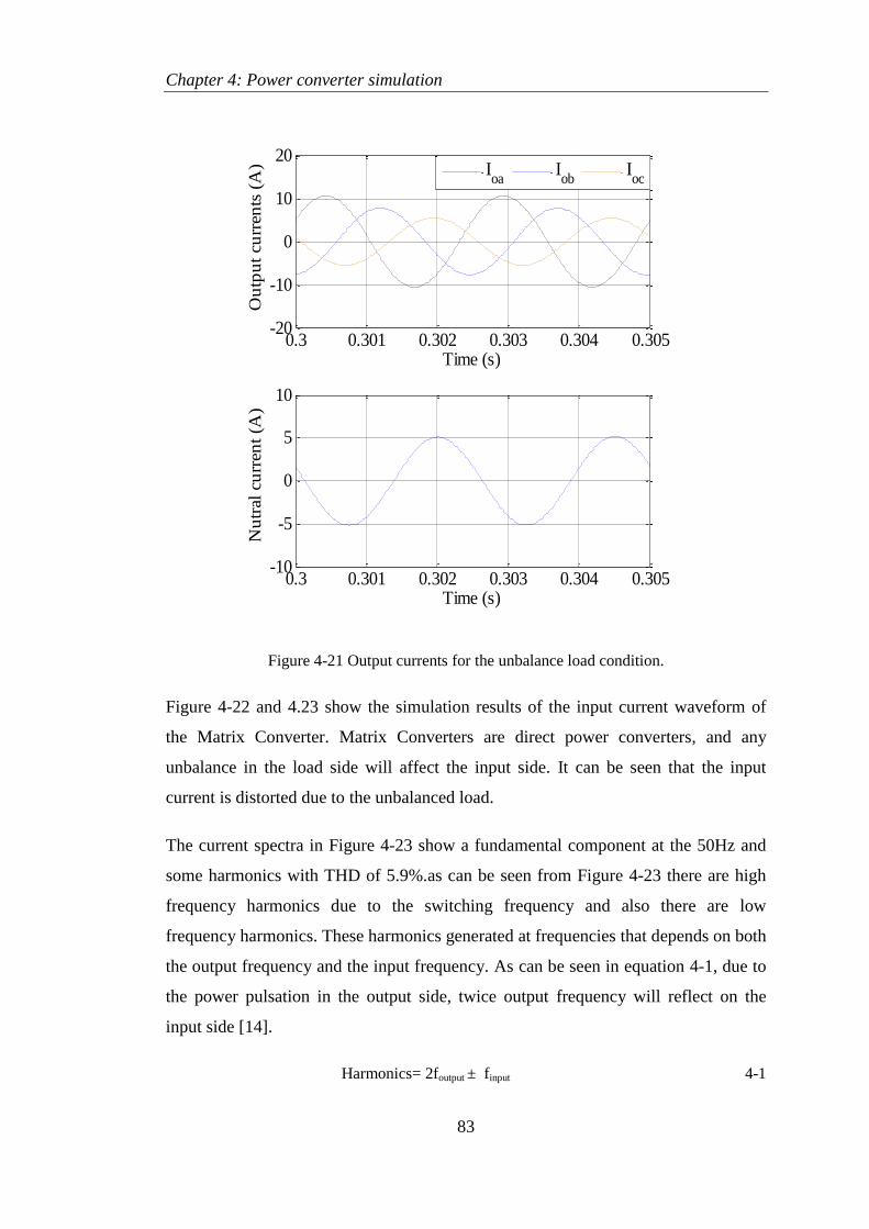
Chapter 4: Power converter simulation
83
Figure 4-21 Output currents for the unbalance load condition.
Figure 4-22 and 4.23 show the simulation results of the input current waveform of
the Matrix Converter. Matrix Converters are direct power converters, and any
unbalance in the load side will affect the input side. It can be seen that the input
current is distorted due to the unbalanced load.
The current spectra in Figure 4-23 show a fundamental component at the 50Hz and
some harmonics with THD of 5.9%.as can be seen from Figure 4-23 there are high
frequency harmonics due to the switching frequency and also there are low
frequency harmonics. These harmonics generated at frequencies that depends on both
the output frequency and the input frequency. As can be seen in equation 4-1, due to
the power pulsation in the output side, twice output frequency will reflect on the
input side [14].
Harmonics= 2foutput ± finput 4-1
0.3 0.301 0.302 0.303 0.304 0.305-20
-10
0
10
20
Time (s)
Ou
tpu
t cu
rren
ts (
A)
0.3 0.301 0.302 0.303 0.304 0.305-10
-5
0
5
10
Time (s)
Nu
tral
cu
rren
t (A
)
Ioa
Iob
Ioc
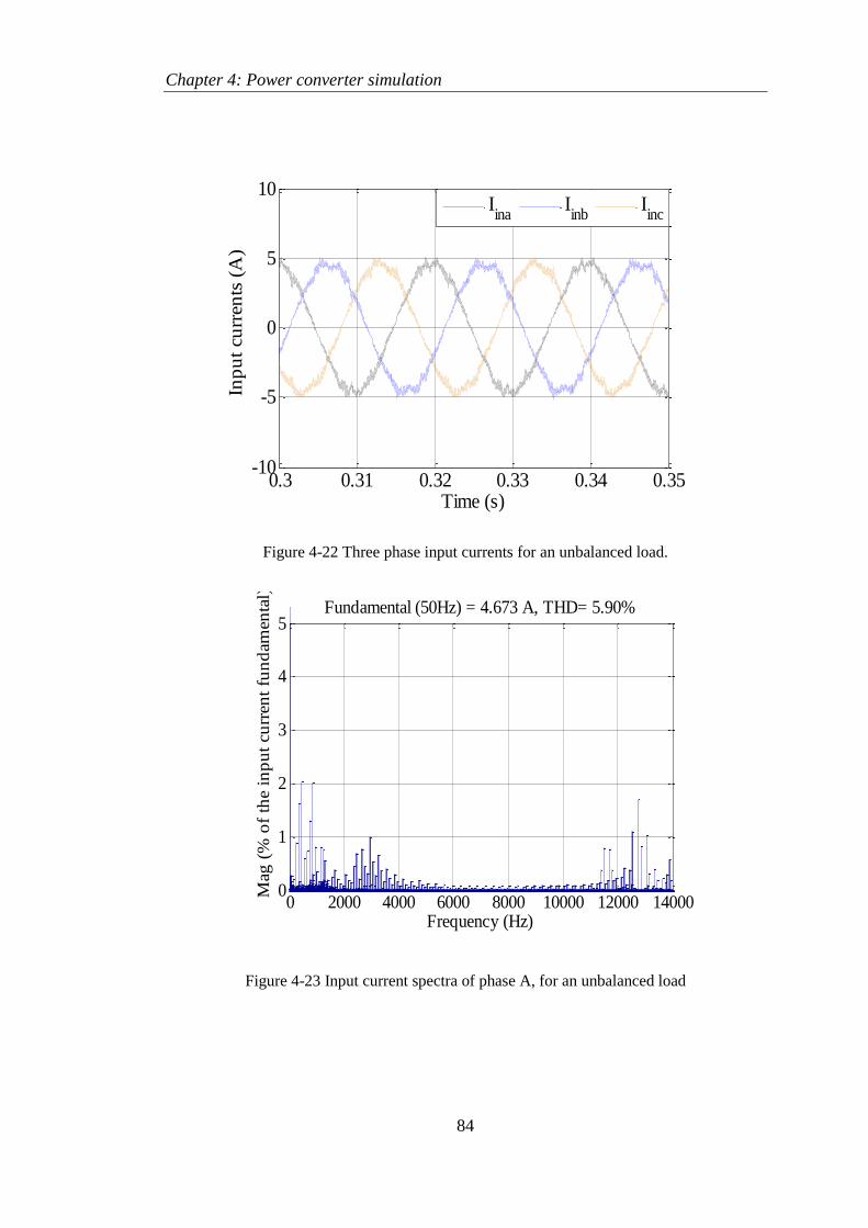
Chapter 4: Power converter simulation
84
Figure 4-22 Three phase input currents for an unbalanced load.
Figure 4-23 Input current spectra of phase A, for an unbalanced load
0.3 0.31 0.32 0.33 0.34 0.35-10
-5
0
5
10
Time (s)
Inp
ut
curr
ents
(A
)
Iina
Iinb
Iinc
0 2000 4000 6000 8000 10000 12000 140000
1
2
3
4
5
Frequency (Hz)
Fundamental (50Hz) = 4.673 A, THD= 5.90%
Mag
(%
of
the
inp
ut
curr
ent
fun
dam
enta
l)
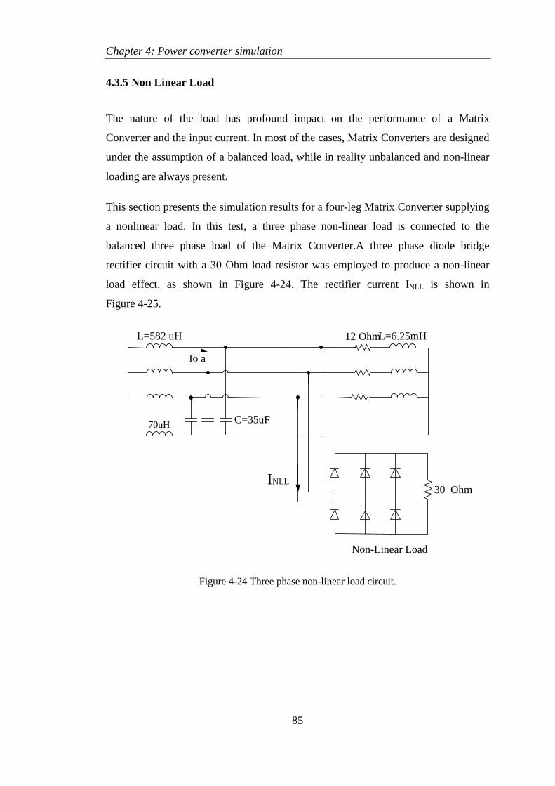
Chapter 4: Power converter simulation
85
4.3.5 Non Linear Load
The nature of the load has profound impact on the performance of a Matrix
Converter and the input current. In most of the cases, Matrix Converters are designed
under the assumption of a balanced load, while in reality unbalanced and non-linear
loading are always present.
This section presents the simulation results for a four-leg Matrix Converter supplying
a nonlinear load. In this test, a three phase non-linear load is connected to the
balanced three phase load of the Matrix Converter.A three phase diode bridge
rectifier circuit with a 30 Ohm load resistor was employed to produce a non-linear
load effect, as shown in Figure 4-24. The rectifier current INLL is shown in
Figure 4-25.
C=35uF
L=6.25mH12 Ohm
Io a
30 Ohm
Non-Linear Load
L=582 uH
70uH
INLL
Figure 4-24 Three phase non-linear load circuit.
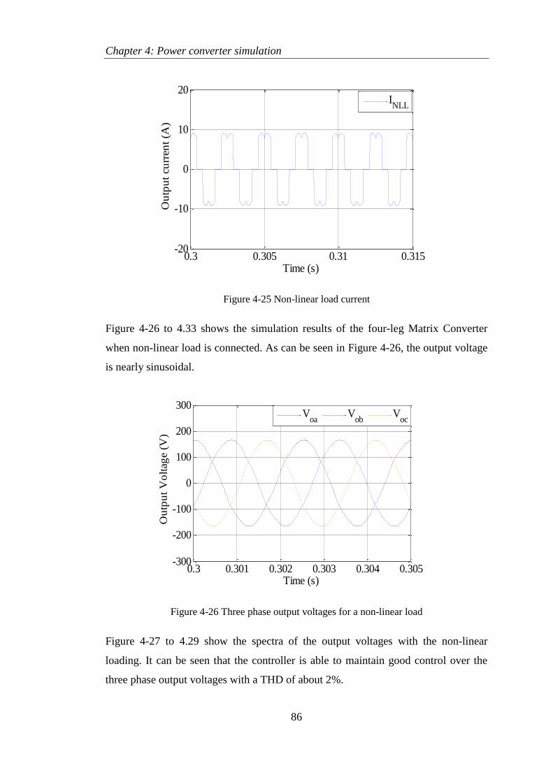
Chapter 4: Power converter simulation
86
Figure 4-25 Non-linear load current
Figure 4-26 to 4.33 shows the simulation results of the four-leg Matrix Converter
when non-linear load is connected. As can be seen in Figure 4-26, the output voltage
is nearly sinusoidal.
Figure 4-26 Three phase output voltages for a non-linear load
Figure 4-27 to 4.29 show the spectra of the output voltages with the non-linear
loading. It can be seen that the controller is able to maintain good control over the
three phase output voltages with a THD of about 2%.
0.3 0.305 0.31 0.315-20
-10
0
10
20
Time (s)
Ou
tpu
t cu
rren
t (A
)
INLL
0.3 0.301 0.302 0.303 0.304 0.305-300
-200
-100
0
100
200
300
Time (s)
Ou
tpu
t V
olt
age
(V)
V
oaV
obV
oc
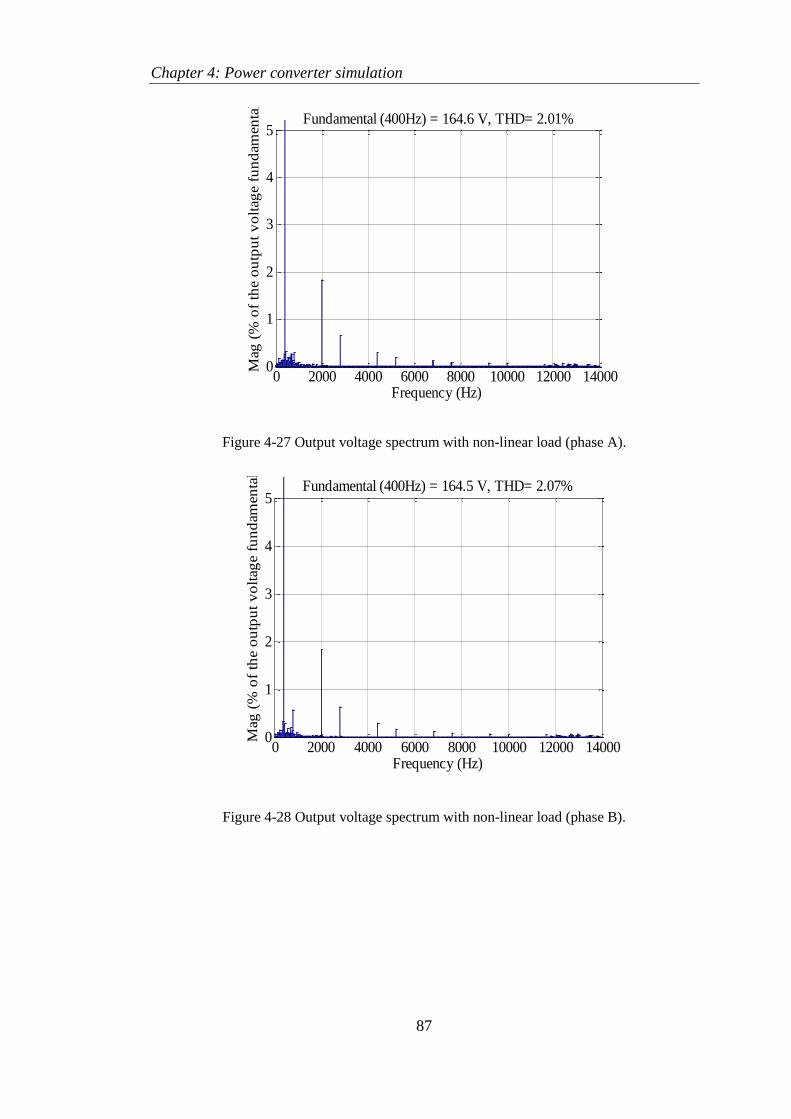
Chapter 4: Power converter simulation
87
Figure 4-27 Output voltage spectrum with non-linear load (phase A).
Figure 4-28 Output voltage spectrum with non-linear load (phase B).
0 2000 4000 6000 8000 10000 12000 140000
1
2
3
4
5
Frequency (Hz)
Fundamental (400Hz) = 164.6 V, THD= 2.01%
Mag
(%
of
the
ou
tpu
t v
olt
age
fun
dam
enta
l)
0 2000 4000 6000 8000 10000 12000 140000
1
2
3
4
5
Frequency (Hz)
Fundamental (400Hz) = 164.5 V, THD= 2.07%
Mag
(%
of
the
ou
tpu
t v
olt
age
fun
dam
enta
l)
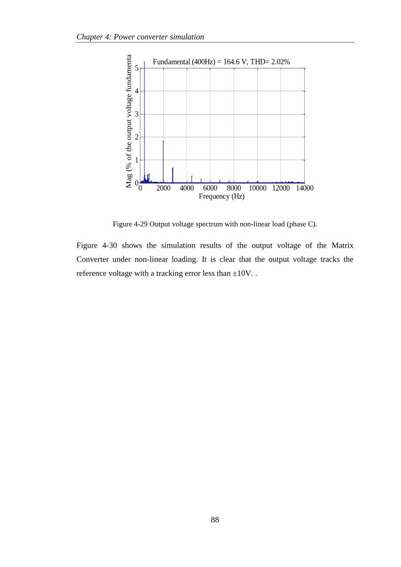
Chapter 4: Power converter simulation
88
Figure 4-29 Output voltage spectrum with non-linear load (phase C).
Figure 4-30 shows the simulation results of the output voltage of the Matrix
Converter under non-linear loading. It is clear that the output voltage tracks the
reference voltage with a tracking error less than ±10V. .
0 2000 4000 6000 8000 10000 12000 140000
1
2
3
4
5
Frequency (Hz)
Fundamental (400Hz) = 164.6 V, THD= 2.02%
Mag
(%
of
the
ou
tpu
t v
olt
age
fun
dam
enta
l)
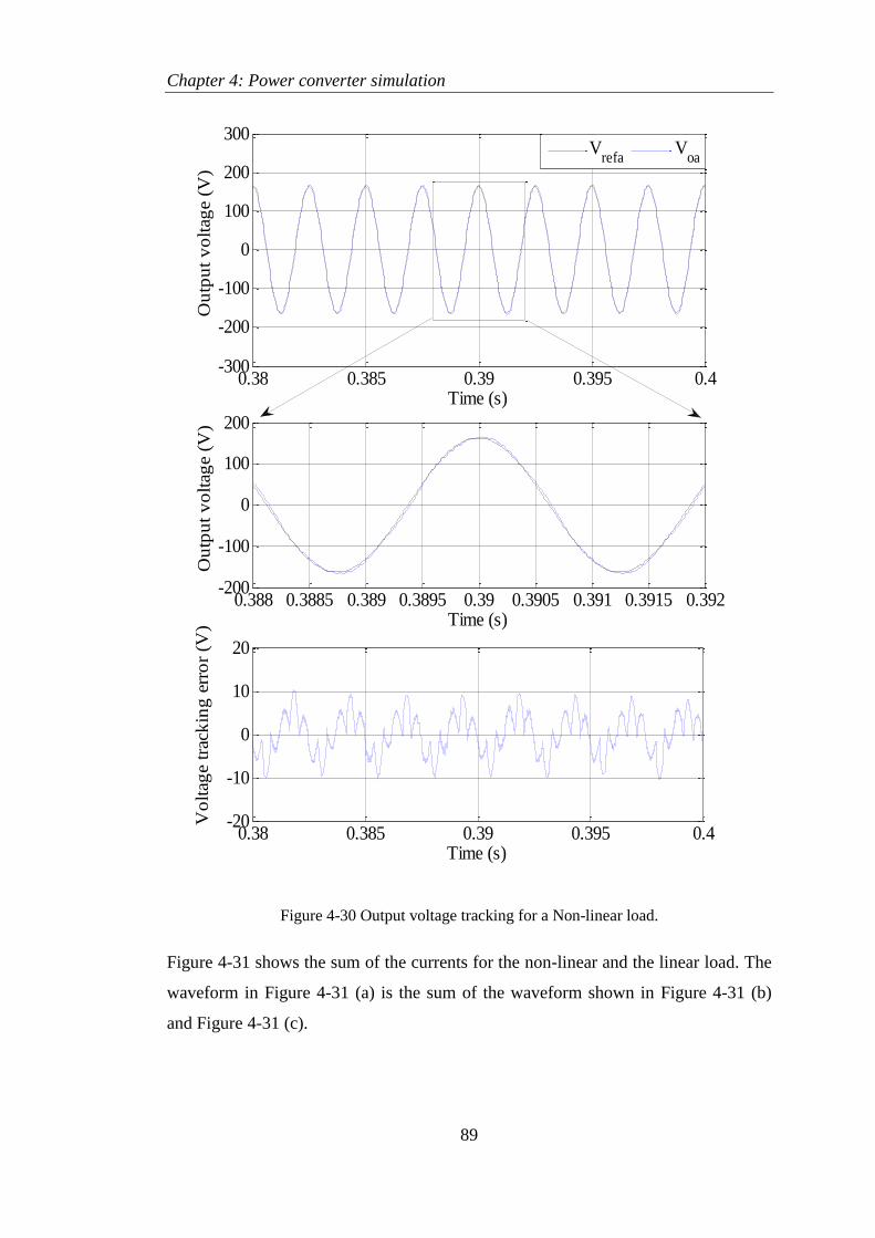
Chapter 4: Power converter simulation
89
Figure 4-30 Output voltage tracking for a Non-linear load.
Figure 4-31 shows the sum of the currents for the non-linear and the linear load. The
waveform in Figure 4-31 (a) is the sum of the waveform shown in Figure 4-31 (b)
and Figure 4-31 (c).
0.38 0.385 0.39 0.395 0.4-300
-200
-100
0
100
200
300
Time (s)
Ou
tpu
t v
olt
age
(V)
V
refaV
oa
0.38 0.385 0.39 0.395 0.4-20
-10
0
10
20
Time (s)
Vo
ltag
e tr
ack
ing
err
or
(V)
0.388 0.3885 0.389 0.3895 0.39 0.3905 0.391 0.3915 0.392-200
-100
0
100
200
Time (s)
Ou
tpu
t v
olt
age
(V)
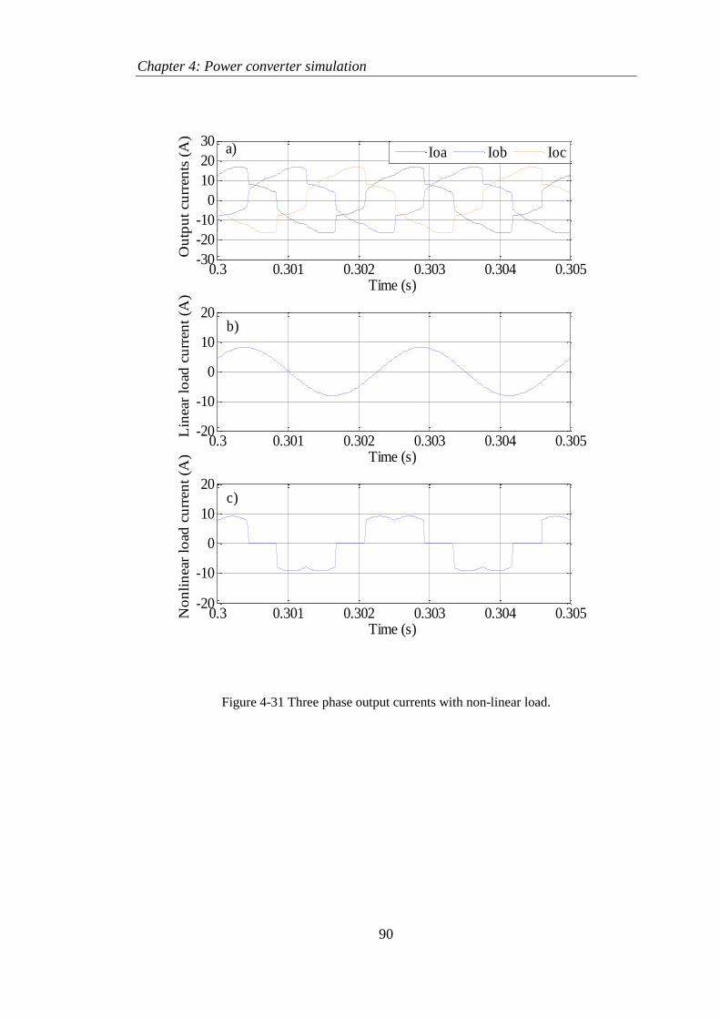
Chapter 4: Power converter simulation
90
Figure 4-31 Three phase output currents with non-linear load.
0.3 0.301 0.302 0.303 0.304 0.305-30
-20
-10
0
10
20
30
Time (s)
Ou
tpu
t cu
rren
ts (
A)
Ioa Iob Ioc
0.3 0.301 0.302 0.303 0.304 0.305-20
-10
0
10
20
Time (s)
Lin
ear
load
cu
rren
t (A
)
0.3 0.301 0.302 0.303 0.304 0.305-20
-10
0
10
20
Time (s)
No
nli
nea
r lo
ad c
urr
ent
(A)
c)
b)
a)
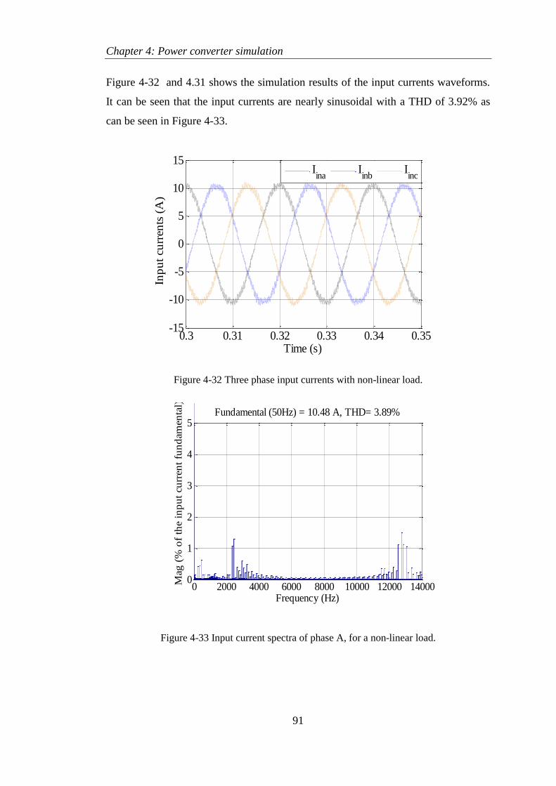
Chapter 4: Power converter simulation
91
Figure 4-32 and 4.31 shows the simulation results of the input currents waveforms.
It can be seen that the input currents are nearly sinusoidal with a THD of 3.92% as
can be seen in Figure 4-33.
Figure 4-32 Three phase input currents with non-linear load.
Figure 4-33 Input current spectra of phase A, for a non-linear load.
0.3 0.31 0.32 0.33 0.34 0.35-15
-10
-5
0
5
10
15
Time (s)
Inp
ut
curr
ents
(A
)
Iina
Iinb
Iinc
0 2000 4000 6000 8000 10000 12000 140000
1
2
3
4
5
Frequency (Hz)
Fundamental (50Hz) = 10.48 A, THD= 3.89%
Mag
(%
of
the
inp
ut
curr
ent
fun
dam
enta
l)

Chapter 4: Power converter simulation
92
4.3.6 Load disconnection and connection
Power converters, regardless of their application, may be used under very light or no
load condition and the controller must be able to maintain proper operation under
these conditions. In this section the simulation results for the four-leg Matrix
Converter is shown during load connection and disconnection.
Figure 4-34 and Figure 4.33 shows the simulation results for the Matrix Converter
during load disconnection and connection. The load is disconnected and reconnected
to test the performance of the converter for a step change in output in output current.
As can be seen from these results, the controller was able to provide good waveform
quality with only a less than 23% output voltage overshoot / under shoot for each
transient.
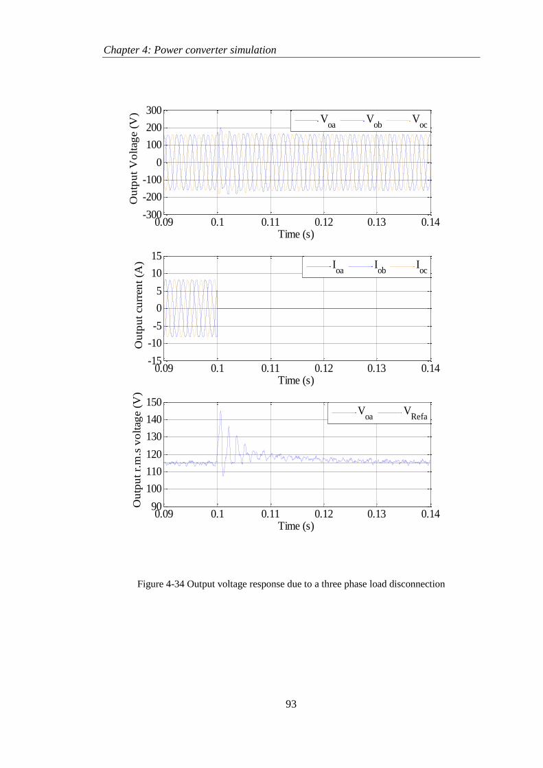
Chapter 4: Power converter simulation
93
Figure 4-34 Output voltage response due to a three phase load disconnection
0.09 0.1 0.11 0.12 0.13 0.14-300
-200
-100
0
100
200
300
Time (s)
Ou
tpu
t V
olt
age
(V)
V
oaV
obV
oc
0.09 0.1 0.11 0.12 0.13 0.14-15
-10
-5
0
5
10
15
Time (s)
Ou
tpu
t cu
rren
t (A
)
Ioa
Iob
Ioc
0.09 0.1 0.11 0.12 0.13 0.1490
100
110
120
130
140
150
Time (s)
Ou
tpu
t r.
m.s
vo
ltag
e (V
)
V
oaV
Refa
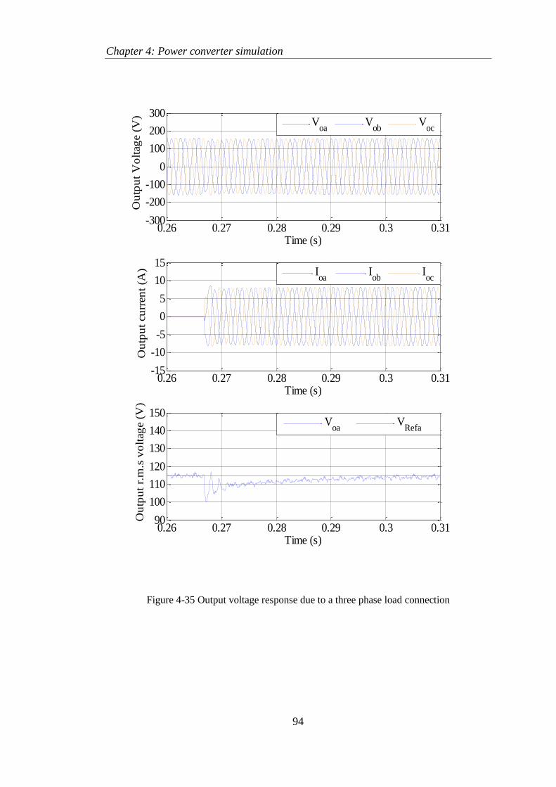
Chapter 4: Power converter simulation
94
Figure 4-35 Output voltage response due to a three phase load connection
0.26 0.27 0.28 0.29 0.3 0.31-300
-200
-100
0
100
200
300
Time (s)
Ou
tpu
t V
olt
age
(V)
V
oaV
obV
oc
0.26 0.27 0.28 0.29 0.3 0.31-15
-10
-5
0
5
10
15
Time (s)
Ou
tpu
t cu
rren
t (A
)
Ioa
Iob
Ioc
0.26 0.27 0.28 0.29 0.3 0.3190
100
110
120
130
140
150
Time (s)
Ou
tpu
t r.
m.s
vo
ltag
e (V
)
V
oaV
Refa
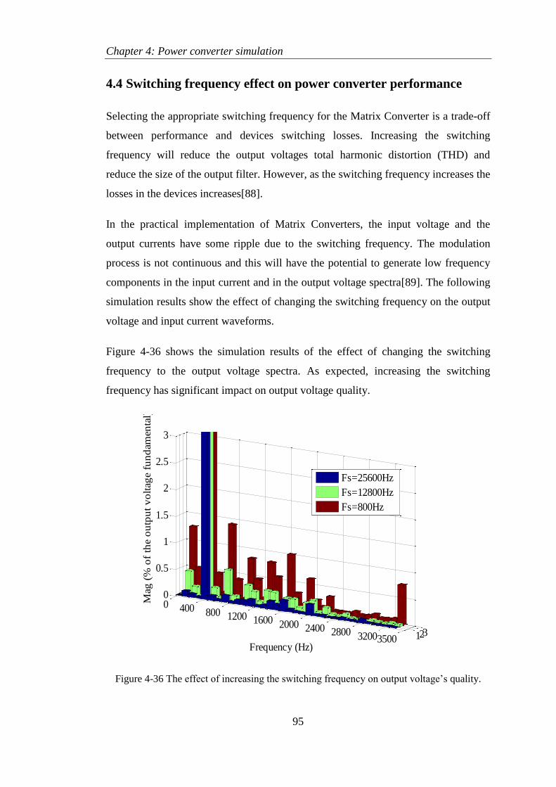
Chapter 4: Power converter simulation
95
4.4 Switching frequency effect on power converter performance
Selecting the appropriate switching frequency for the Matrix Converter is a trade-off
between performance and devices switching losses. Increasing the switching
frequency will reduce the output voltages total harmonic distortion (THD) and
reduce the size of the output filter. However, as the switching frequency increases the
losses in the devices increases[88].
In the practical implementation of Matrix Converters, the input voltage and the
output currents have some ripple due to the switching frequency. The modulation
process is not continuous and this will have the potential to generate low frequency
components in the input current and in the output voltage spectra[89]. The following
simulation results show the effect of changing the switching frequency on the output
voltage and input current waveforms.
Figure 4-36 shows the simulation results of the effect of changing the switching
frequency to the output voltage spectra. As expected, increasing the switching
frequency has significant impact on output voltage quality.
Figure 4-36 The effect of increasing the switching frequency on output voltage’s quality.
123
0 400 800 1200 1600 2000 2400 2800 32003500
0
0.5
1
1.5
2
2.5
3
Frequency (Hz)
Mag
(%
of
the
ou
tpu
t v
olt
age
fun
dam
enta
l)
Fs=25600Hz
Fs=12800Hz
Fs=800Hz

Chapter 4: Power converter simulation
96
Low and high frequency components are normally exist in the input current and the
output voltage waveforms. The low frequency components are due to several reasons
such as the modulation method, the switching ripples in the input current and voltage
waveforms, because of the digital implementation of the controller and modulation
algorithms and due to the nonlinearities of the Matrix Converter itself. All of the
above have the potential to generate low frequency components in the output voltage
and input current spectra.
The high frequency components are normally generated due to the switching
frequencies and it can be seen very clearly in the input current waveform. This high
switching frequency can be minimized by using an input filter at the input side to
provide a path to the high frequency components.
The lower the switching frequency the more the distortion of the output voltage and
input current waveforms, and the bigger the filters and it becomes more difficult to
control the converter especially at 400Hz applications where the controller
bandwidth cannot be made high.
Circuit setup shown in Figure 4-3 is used throughout the study of the effect of the
switching frequency on the Matrix Converter performance. The input filter the output
filter, the modulation and the controller details are all fixed during the study. The
following sections will present the simulation results of the four-leg Matrix
Converter for different switching frequency starting from 8kHz to 12.8kHz and
finally with 25.6kHz.
4.4.1 Simulation results using 8kHz switching frequency
Figure 4-37 to Figure 4.41 shows the simulation results of the four-leg Matrix
Converter using 8 kHz switching frequency. As shown in Figure 4-37 the output
voltage waveforms are nearly sinusoidal with some ripples. Figure 4-38 shows the
spectrum of the output voltage with THD of 1.13%.
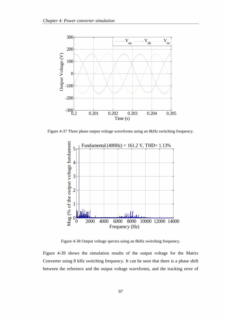
Chapter 4: Power converter simulation
97
Figure 4-37 Three phase output voltage waveforms using an 8kHz switching frequency.
Figure 4-38 Output voltage spectra using an 8kHz switching frequency.
Figure 4-39 shows the simulation results of the output voltage for the Matrix
Converter using 8 kHz switching frequency. It can be seen that there is a phase shift
between the reference and the output voltage waveforms, and the tracking error of
0.2 0.201 0.202 0.203 0.204 0.205-300
-200
-100
0
100
200
300
Time (s)
Ou
tpu
t V
olt
age
(V)
V
oaV
obV
oc
0 2000 4000 6000 8000 10000 12000 140000
1
2
3
4
5
Frequency (Hz)
Fundamental (400Hz) = 161.2 V, THD= 1.13%
Mag
(%
of
the
ou
tpu
t v
olt
age
fun
dam
enta
l)
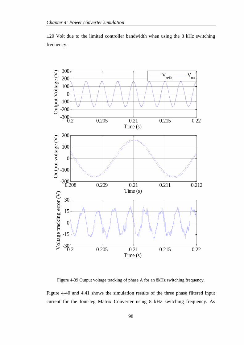
Chapter 4: Power converter simulation
98
±20 Volt due to the limited controller bandwidth when using the 8 kHz switching
frequency.
Figure 4-39 Output voltage tracking of phase A for an 8kHz switching frequency.
Figure 4-40 and 4.41 shows the simulation results of the three phase filtered input
current for the four-leg Matrix Converter using 8 kHz switching frequency. As
0.2 0.205 0.21 0.215 0.22-300
-200
-100
0
100
200
300
Time (s)
Ou
tpu
t V
olt
age
(V)
V
refaV
oa
0.208 0.209 0.21 0.211 0.212-200
-100
0
100
200
Time (s)
Ou
tpu
t v
olt
age
(V)
0.2 0.205 0.21 0.215 0.22-30
-15
0
15
30
Time (s)
Vo
ltag
e tr
ack
ing
err
or
(V)
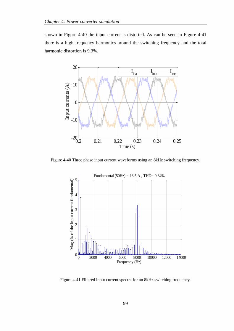
Chapter 4: Power converter simulation
99
shown in Figure 4-40 the input current is distorted. As can be seen in Figure 4-41
there is a high frequency harmonics around the switching frequency and the total
harmonic distortion is 9.3%.
Figure 4-40 Three phase input current waveforms using an 8kHz switching frequency.
Figure 4-41 Filtered input current spectra for an 8kHz switching frequency.
0.2 0.21 0.22 0.23 0.24 0.25-20
-10
0
10
20
Time (s)
Inp
ut
curr
ents
(A
)
Iina
Iinb
Iinc
0 2000 4000 6000 8000 10000 12000 140000
1
2
3
4
5
Frequency (Hz)
Fundamental (50Hz) = 13.5 A , THD= 9.34%
Mag
(%
of
the
inp
ut
curr
ent
fun
dam
enta
l)
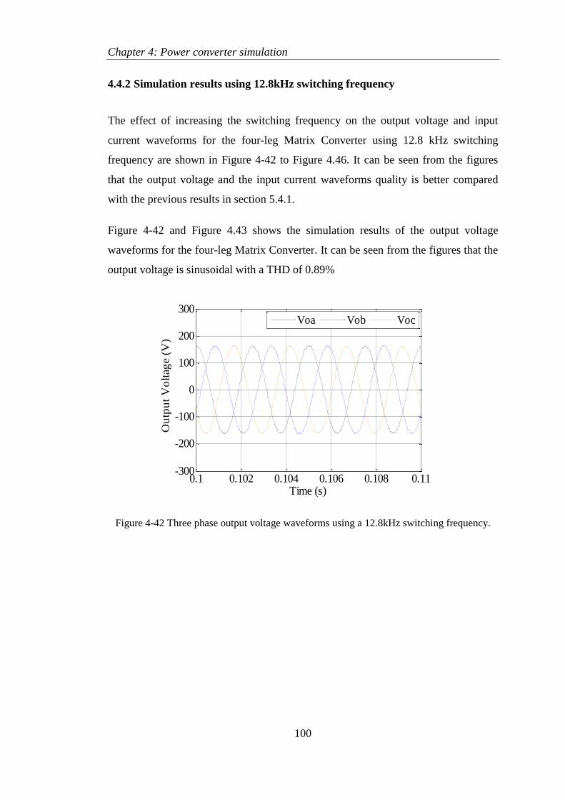
Chapter 4: Power converter simulation
100
4.4.2 Simulation results using 12.8kHz switching frequency
The effect of increasing the switching frequency on the output voltage and input
current waveforms for the four-leg Matrix Converter using 12.8 kHz switching
frequency are shown in Figure 4-42 to Figure 4.46. It can be seen from the figures
that the output voltage and the input current waveforms quality is better compared
with the previous results in section 5.4.1.
Figure 4-42 and Figure 4.43 shows the simulation results of the output voltage
waveforms for the four-leg Matrix Converter. It can be seen from the figures that the
output voltage is sinusoidal with a THD of 0.89%
Figure 4-42 Three phase output voltage waveforms using a 12.8kHz switching frequency.
0.1 0.102 0.104 0.106 0.108 0.11-300
-200
-100
0
100
200
300
Time (s)
Ou
tpu
t V
olt
age
(V)
Voa Vob Voc
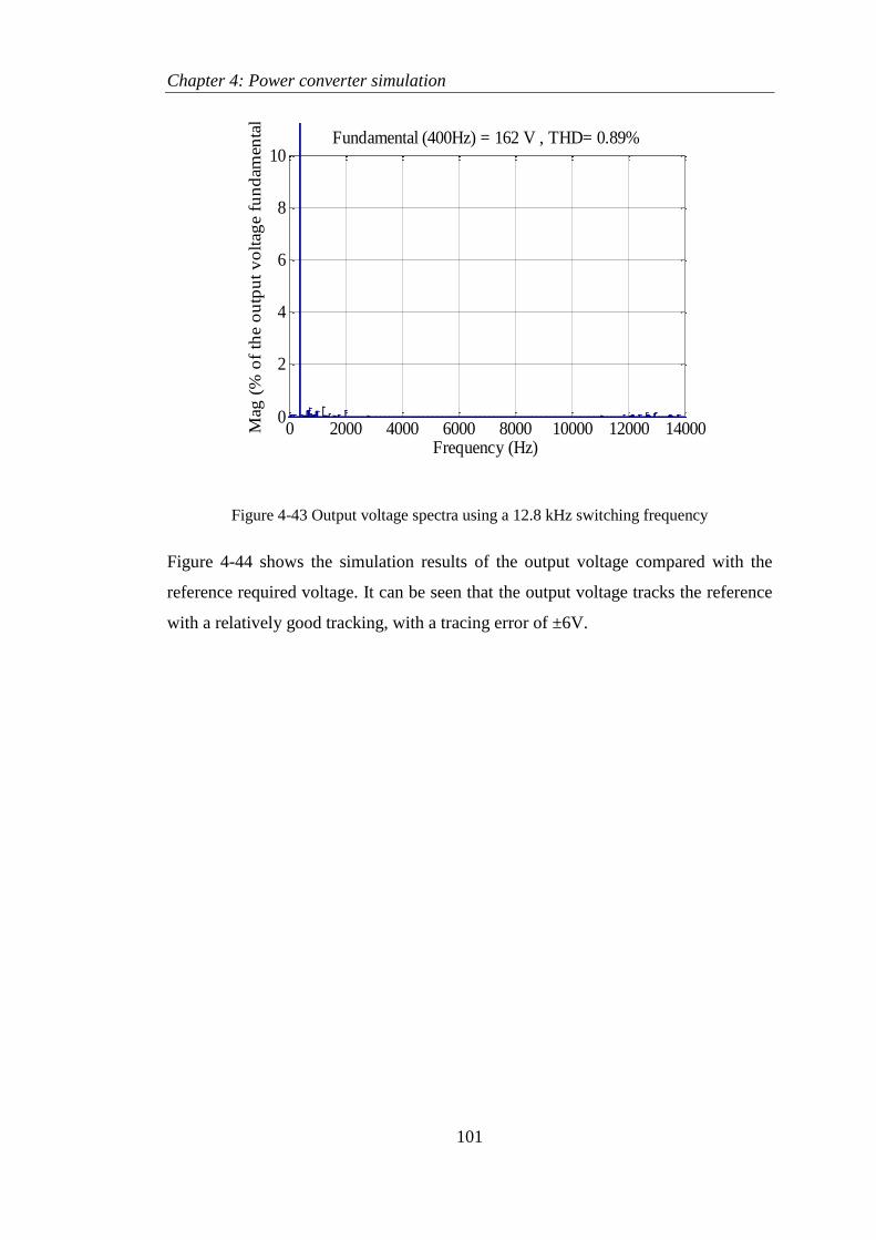
Chapter 4: Power converter simulation
101
Figure 4-43 Output voltage spectra using a 12.8 kHz switching frequency
Figure 4-44 shows the simulation results of the output voltage compared with the
reference required voltage. It can be seen that the output voltage tracks the reference
with a relatively good tracking, with a tracing error of ±6V.
0 2000 4000 6000 8000 10000 12000 140000
2
4
6
8
10
Frequency (Hz)
Fundamental (400Hz) = 162 V , THD= 0.89%
Mag
(%
of
the
ou
tpu
t v
olt
age
fun
dam
enta
l )
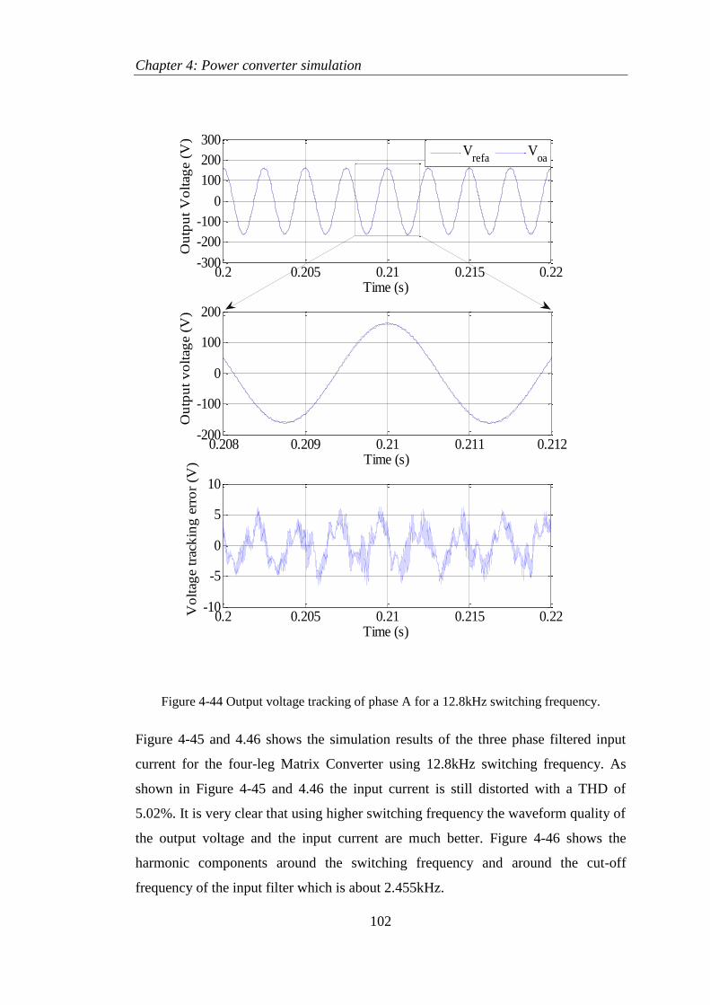
Chapter 4: Power converter simulation
102
Figure 4-44 Output voltage tracking of phase A for a 12.8kHz switching frequency.
Figure 4-45 and 4.46 shows the simulation results of the three phase filtered input
current for the four-leg Matrix Converter using 12.8kHz switching frequency. As
shown in Figure 4-45 and 4.46 the input current is still distorted with a THD of
5.02%. It is very clear that using higher switching frequency the waveform quality of
the output voltage and the input current are much better. Figure 4-46 shows the
harmonic components around the switching frequency and around the cut-off
frequency of the input filter which is about 2.455kHz.
0.2 0.205 0.21 0.215 0.22-300
-200
-100
0
100
200
300
Time (s)
Ou
tpu
t V
olt
age
(V)
V
refaV
oa
0.208 0.209 0.21 0.211 0.212-200
-100
0
100
200
Time (s)
Ou
tpu
t v
olt
age
(V)
0.2 0.205 0.21 0.215 0.22-10
-5
0
5
10
Time (s)
Vo
ltag
e tr
ack
ing
err
or
(V)
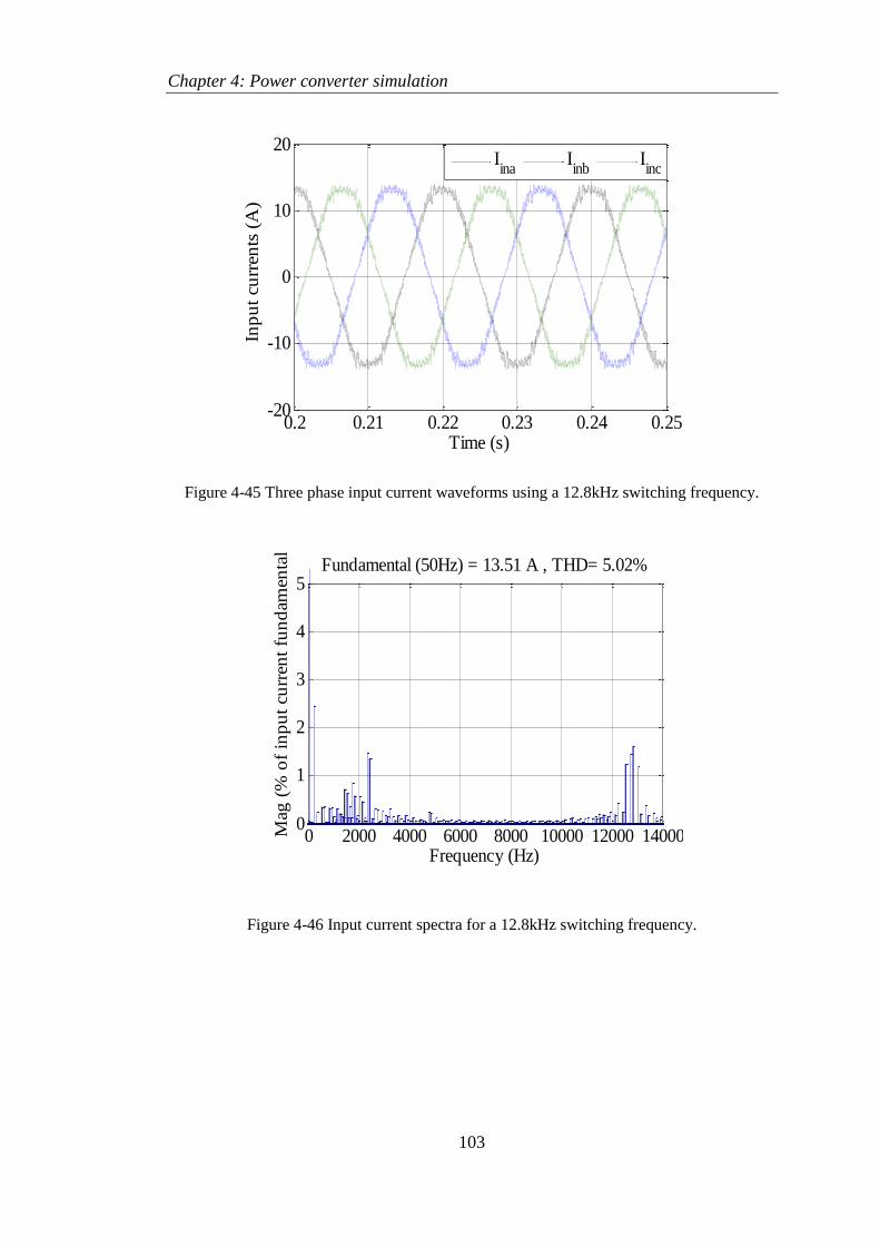
Chapter 4: Power converter simulation
103
Figure 4-45 Three phase input current waveforms using a 12.8kHz switching frequency.
Figure 4-46 Input current spectra for a 12.8kHz switching frequency.
0.2 0.21 0.22 0.23 0.24 0.25-20
-10
0
10
20
Time (s)
Inp
ut
curr
ents
(A
)
Iina
Iinb
Iinc
0 2000 4000 6000 8000 10000 12000 140000
1
2
3
4
5
Frequency (Hz)
Fundamental (50Hz) = 13.51 A , THD= 5.02%
Mag
(%
of
inp
ut
curr
ent
fun
dam
enta
l)
Chapter 4: Power converter simulation
104
4.4.3 Simulation results using 25.6kHz switching frequency
Simulation results of the four-leg Matrix Converter using 25.6 kHz switching
frequency is shown in Figure 4-47 to Figure 4.51. It can be seen that the output
voltage and current waveforms quality are much better than the previous results in
section 5.4.1 and 5.4.2. Figure 4-47 and 4.48 shows the output voltage waveforms
and spectra. It can be seen that the output voltage waveform in sinusoidal with THD
of 0.52%. And the low and high order harmonic components are significantly
reduced, and the output voltage ripples are minimized with the use of 25.6kHz
switching frequency.
Figure 4-47 Three phase output voltage waveforms using a 25.6kHz switching frequency.
0.1 0.102 0.104 0.106 0.108 0.11-300
-200
-100
0
100
200
300
Time (s)
Ou
tpu
t V
olt
age
(V)
Voa Vob Voc
Chapter 4: Power converter simulation
105
Figure 4-48 Output voltage spectra using a 25.6 kHz switching frequency
Figure 4-49 shows the simulation results of the output voltage compared with the
reference voltage. It can be seen that the output voltage tracks the reference voltage,
with a tracking error less than ±4V.
0 0.5 1 1.5 2 2.5 3
x 104
0
1
2
3
4
5
Frequency (Hz)
Fundamental (400Hz) = 162.6 V , THD= 0.52%
Mag
(%
of
ou
tpu
t v
olt
age
fun
dam
enta
l)
Chapter 4: Power converter simulation
106
Figure 4-49 Output voltage tracking of phase A for a 25.6kHz switching frequency.
Figure 4-50 and 4.51 shows the simulation results of the three phase filtered input
current for the four-leg Matrix Converter using 25.6 kHz switching frequency. As
shown in Figure 4-50 and 4.51 the input current is still distorted with a THD of 4.3%.
It is very clear that by increasing the switching frequency to 25.6kHz the waveform
quality of the output voltage and the input current are improved. Figure 4-51 shows
that there are harmonic components around the switching frequency and around the
cut-off frequency of the input filter which is about 2.455kHz.
0.2 0.205 0.21 0.215 0.22-300
-200
-100
0
100
200
300
Time (s)
Ou
tpu
t V
olt
age
(V)
V
refaV
oa
0.208 0.209 0.21 0.211 0.212-200
-100
0
100
200
Time (s)
Ou
tpu
t v
olt
age
(V)
0.2 0.205 0.21 0.215 0.22-10
-5
0
5
10
Time (s)
Vo
ltag
e tr
ack
ing
err
or
(V)
Chapter 4: Power converter simulation
107
Figure 4-50 Three phase input current waveforms using a 25.6kHz switching frequency.
Figure 4-51 Input current spectra for a 25.6kHz switching frequency.
0.2 0.21 0.22 0.23 0.24 0.25-20
-10
0
10
20
Time (s)
Inp
ut
curr
ents
(A
)
Iina
Iinb
Iinc
0 0.5 1 1.5 2 2.5 3
x 104
0
1
2
3
4
5
Frequency (Hz)
Fundamental (50Hz) = 13.95A , THD= 4.30%
Mag
(%
of
inp
ut
curr
ent
fun
dam
enta
l)

Chapter 4: Power converter simulation
108
4.5 Summery
In this chapter, a simulation study for Matrix Converter system was carried out using
the Saber simulation package. A second order controller was used in conjunction
with a plug-in repetitive controller to control the output voltage of the Matrix
Converter in ABC reference frame. Extensive simulations of the converter showed
that the proposed controller is able to offer good tracking accuracy, fast transient
response and is able to regulate the output voltage for unbalanced load conditions,
non-linear load conditions and for a load disconnection/reconnection. Table 4-1
present a summary of the results.
Table 4-1 Summary of the simulation results for four-leg Matrix Converter system.
Balanced load
Output voltage THD 0.89%
Tracking error ± 7V
Input current THD 3.71%
Unbalanced load
Output voltage THD 1.33%, 1.39%, 1.44%
Tracking error ± 10V
Input current THD 5.9%
Non-linear load
Output voltage THD 2.02%
Tracking error ± 10V
Input current THD 3.89%
Load connection/disconnection
Overshoot 23%
Undershoot 17%
The effect of changing the switching frequency on the converter performance has
also been presented and the results show that increasing the switching frequency
tends to reduce both of the input current and the output voltage THD and the
associated low frequency ripples in the waveforms.

Chapter 4: Power converter simulation
109
Table 4-2 shows the effect of increasing the switching frequency on Matrix
Converter performance.
Table 4-2 The effect of increasing the switching frequency on Matrix Converter
performance.
Switching frequency
8000 Hz 12800 Hz 25600 Hz
Output voltage THD 1.13% 0.89% 0.52%
Input current THD 9.34% 5.02% 4.3%
Output voltage tracking error ±22 ±6 ±3.5
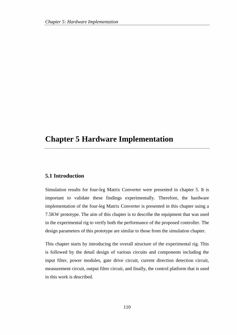
Chapter 5: Hardware Implementation
110
Chapter 5 Hardware Implementation
5.1 Introduction
Simulation results for four-leg Matrix Converter were presented in chapter 5. It is
important to validate these findings experimentally. Therefore, the hardware
implementation of the four-leg Matrix Converter is presented in this chapter using a
7.5KW prototype. The aim of this chapter is to describe the equipment that was used
in the experimental rig to verify both the performance of the proposed controller. The
design parameters of this prototype are similar to those from the simulation chapter.
This chapter starts by introducing the overall structure of the experimental rig. This
is followed by the detail design of various circuits and components including the
input filter, power modules, gate drive circuit, current direction detection circuit,
measurement circuit, output filter circuit, and finally, the control platform that is used
in this work is described.
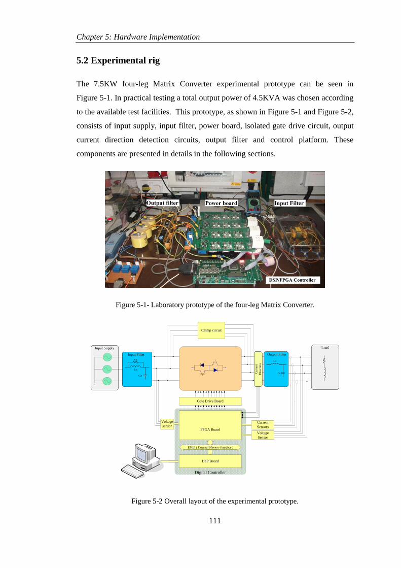
Chapter 5: Hardware Implementation
111
5.2 Experimental rig
The 7.5KW four-leg Matrix Converter experimental prototype can be seen in
Figure 5-1. In practical testing a total output power of 4.5KVA was chosen according
to the available test facilities. This prototype, as shown in Figure 5-1 and Figure 5-2,
consists of input supply, input filter, power board, isolated gate drive circuit, output
current direction detection circuits, output filter and control platform. These
components are presented in details in the following sections.
Figure 5-1- Laboratory prototype of the four-leg Matrix Converter.
LoadInput Supply
Current
Sensors
Voltage
Sensor
Voltage
sensor
Digital Controller
DSP Board
Gate Drive Board
FPGA Board
EMIF ( External Memory Interface )
Clamp circuit
Output Filter
Lo
CoCurr
ent
Dir
ecti
on
Cin
Lin
Rin
Input Filter
Figure 5-2 Overall layout of the experimental prototype.
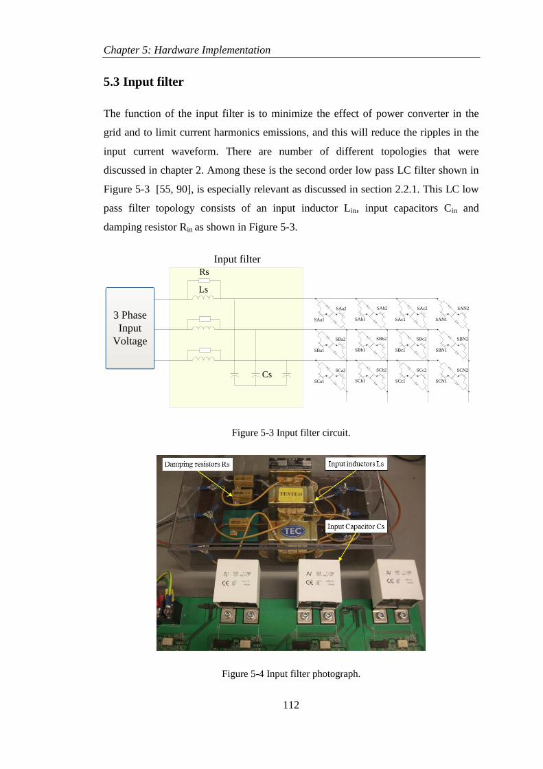
Chapter 5: Hardware Implementation
112
5.3 Input filter
The function of the input filter is to minimize the effect of power converter in the
grid and to limit current harmonics emissions, and this will reduce the ripples in the
input current waveform. There are number of different topologies that were
discussed in chapter 2. Among these is the second order low pass LC filter shown in
Figure 5-3 [55, 90], is especially relevant as discussed in section 2.2.1. This LC low
pass filter topology consists of an input inductor Lin, input capacitors Cin and
damping resistor Rin as shown in Figure 5-3.
Cs
Ls
Rs
Input filter
3 Phase
Input
Voltage
SAa2 SAb2 SAc2 SAN2
SBa2 SBb2 SBc2 SBN2
SCa2 SCb2 SCc2 SCN2
SCa1 SCb1 SCc1 SCN1
SBa1 SBb1 SBc1 SBN1
SAa1 SAb1 SAc1 SAN1
Figure 5-3 Input filter circuit.
Figure 5-4 Input filter photograph.
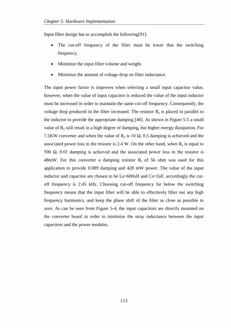
Chapter 5: Hardware Implementation
113
Input filter design has to accomplish the following[91]:
The cut-off frequency of the filter must be lower that the switching
frequency.
Minimize the input filter volume and weight.
Minimize the amount of voltage drop on filter inductance.
The input power factor is improves when selecting a small input capacitor value,
however, when the value of input capacitor is reduced the value of the input inductor
must be increased in order to maintain the same cut-off frequency. Consequently, the
voltage drop produced in the filter increased. The resistor Rs is placed in parallel to
the inductor to provide the appropriate damping [46]. As shown in Figure 5-5 a small
value of Rs will result in a high degree of damping, but higher energy dissipation. For
7.5KW converter and when the value of Rs is 10 Ω, 0.5 damping is achieved and the
associated power loss in the resistor is 2.4 W. On the other hand, when Rs is equal to
500 Ω, 0.01 damping is achieved and the associated power loss in the resistor is
48mW. For this converter a damping resistor Rs of 56 ohm was used for this
application to provide 0.089 damping and 428 mW power. The value of the input
inductor and capacitor are chosen to be Ls=600uH and Cs=2uF, accordingly the cut-
off frequency is 2.45 kHz. Choosing cut-off frequency far below the switching
frequency means that the input filter will be able to effectively filter out any high
frequency harmonics, and keep the phase shift of the filter as close as possible to
zero. As can be seen from Figure 5-4, the input capacitors are directly mounted on
the converter board in order to minimize the stray inductance between the input
capacitors and the power modules.
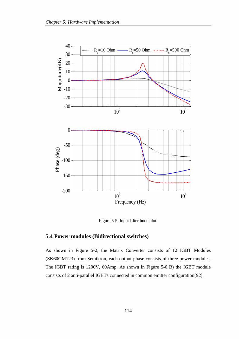
Chapter 5: Hardware Implementation
114
Figure 5-5 Input filter bode plot.
5.4 Power modules (Bidirectional switches)
As shown in Figure 5-2, the Matrix Converter consists of 12 IGBT Modules
(SK60GM123) from Semikron, each output phase consists of three power modules.
The IGBT rating is 1200V, 60Amp. As shown in Figure 5-6 B) the IGBT module
consists of 2 anti-parallel IGBTs connected in common emitter configuration[92].
103
104
-30
-20
-10
0
10
20
30
40
Mag
nit
ud
e(d
B)
103
104
-200
-150
-100
-50
0
Frequency (Hz)
Ph
ase
(deg
)
Rs=10 Ohm R
s=50 Ohm R
s=500 Ohm
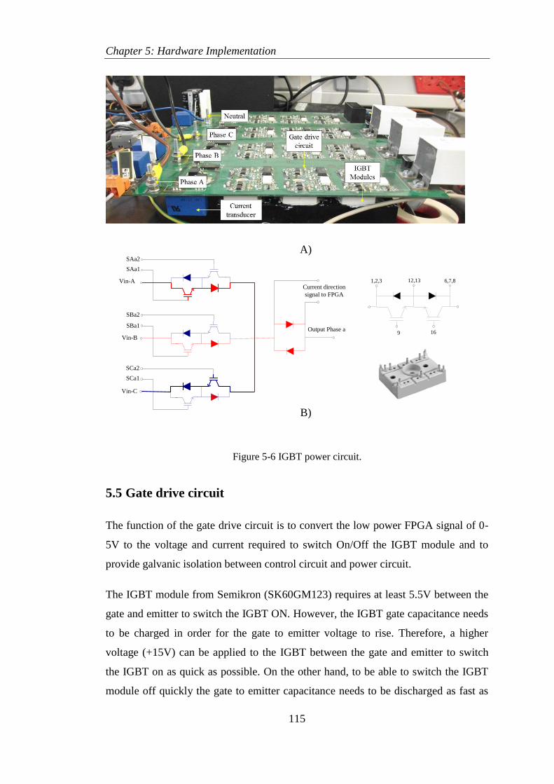
Chapter 5: Hardware Implementation
115
9
1,2,3
16
12,13 6,7,8
Output Phase a
SAa2
SAa1
Vin-A
SBa2
SBa1
Vin-B
SCa2
SCa1
Vin-C
Current direction
signal to FPGA
B)
A)
Figure 5-6 IGBT power circuit.
5.5 Gate drive circuit
The function of the gate drive circuit is to convert the low power FPGA signal of 0-
5V to the voltage and current required to switch On/Off the IGBT module and to
provide galvanic isolation between control circuit and power circuit.
The IGBT module from Semikron (SK60GM123) requires at least 5.5V between the
gate and emitter to switch the IGBT ON. However, the IGBT gate capacitance needs
to be charged in order for the gate to emitter voltage to rise. Therefore, a higher
voltage (+15V) can be applied to the IGBT between the gate and emitter to switch
the IGBT on as quick as possible. On the other hand, to be able to switch the IGBT
module off quickly the gate to emitter capacitance needs to be discharged as fast as

Chapter 5: Hardware Implementation
116
possible. This can be done by Appling negative voltage (-15V) to the IGBT gate with
respect to the emitter. Accordingly, the gate drive circuit is required to provide +15V
or -15 V between the gate and the emitter of the IGBT to switch the IGBT On or Off.
A Texas instrument floating DC/DC converter (DCP020515DU) is used to provide
the gate drive circuit with ±15V an isolated supply. As shown in Figure 5-7, the
signal from FPGA passes through an open drain buffer (SN74LVC1G07) that is used
to protect FPGA and supply the required current to opt-coupler together with the pull
up resistor R9. The buffer output is connected to the opt-coupler (HCPL-315J) which
provides galvanic isolation between control and power circuits. The opt-coupler
output is connected to a push pull transistor circuit implemented using NPN and PNP
transistors (FZT790A and FTZ690B) to provide the required current and voltage to
switch IGBT through a gate drive resistor (R11 or R16) The choice of R11 or R16
affects the On/Off switching times and switching losses [57].
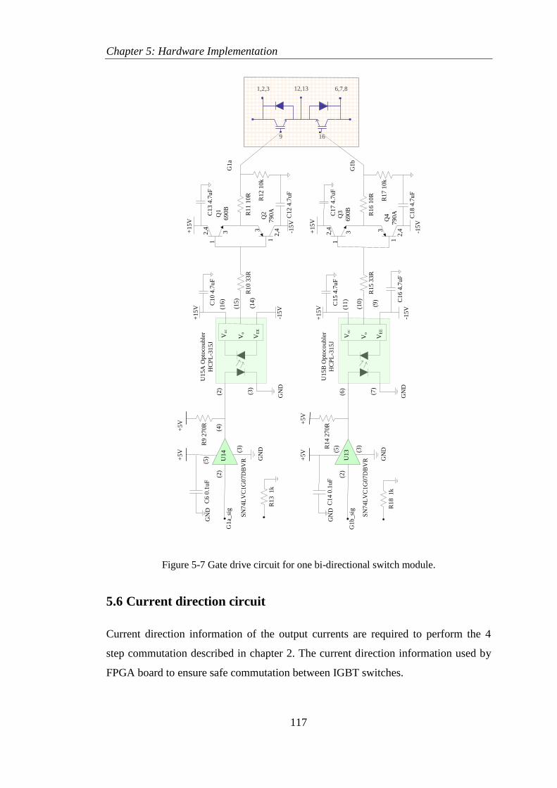
Chapter 5: Hardware Implementation
117
C6 0
.1uF
R9 2
70R
+5V
GN
D
GN
D
GN
D
+5V
(2)
( 3)
(5)
(4)
G1a_
sig
Vcc
Vo
VE
E
+15V
- 15V
R10 3
3R
(2)
( 3)
(16)
( 15)
(14)
+15V
-15V
R11 1
0R
C12 4
. 7uF
R12 1
0k
Q2
790A
G1a
C13 4
.7uF
12,4 3 3
2, 4
1
C10 4
.7uF
R13 1k
GN
DC
14 0
.1uF
R14 2
70R
+5V
GN
D
GN
D
+5V
(2)
(3)
( 5)
G1b_si
gV
cc
Vo
VE
E
+15V
- 15
V
R15 3
3R
( 6)
( 7)
(11)
( 10)
( 9)
+15V
-15V
R16 1
0R
C18 4
.7uF
R17 1
0k
Q4
790A
G1b
12,4 3 3
2, 4
1
C15 4
.7uF
C17 4
. 7uF
C16 4
.7uF
R18 1
k
1,2,3
9 16
6,7,812,13
Q1
690B
Q3
690B
U15A
Opto
couble
r
HC
PL
-315J
U15B
Opto
couble
r
HC
PL
- 315J
U14
U13
SN
74L
VC
1G
07
DB
VR
SN
74L
VC
1G
07
DB
VR
Figure 5-7 Gate drive circuit for one bi-directional switch module.
5.6 Current direction circuit
Current direction information of the output currents are required to perform the 4
step commutation described in chapter 2. The current direction information used by
FPGA board to ensure safe commutation between IGBT switches.
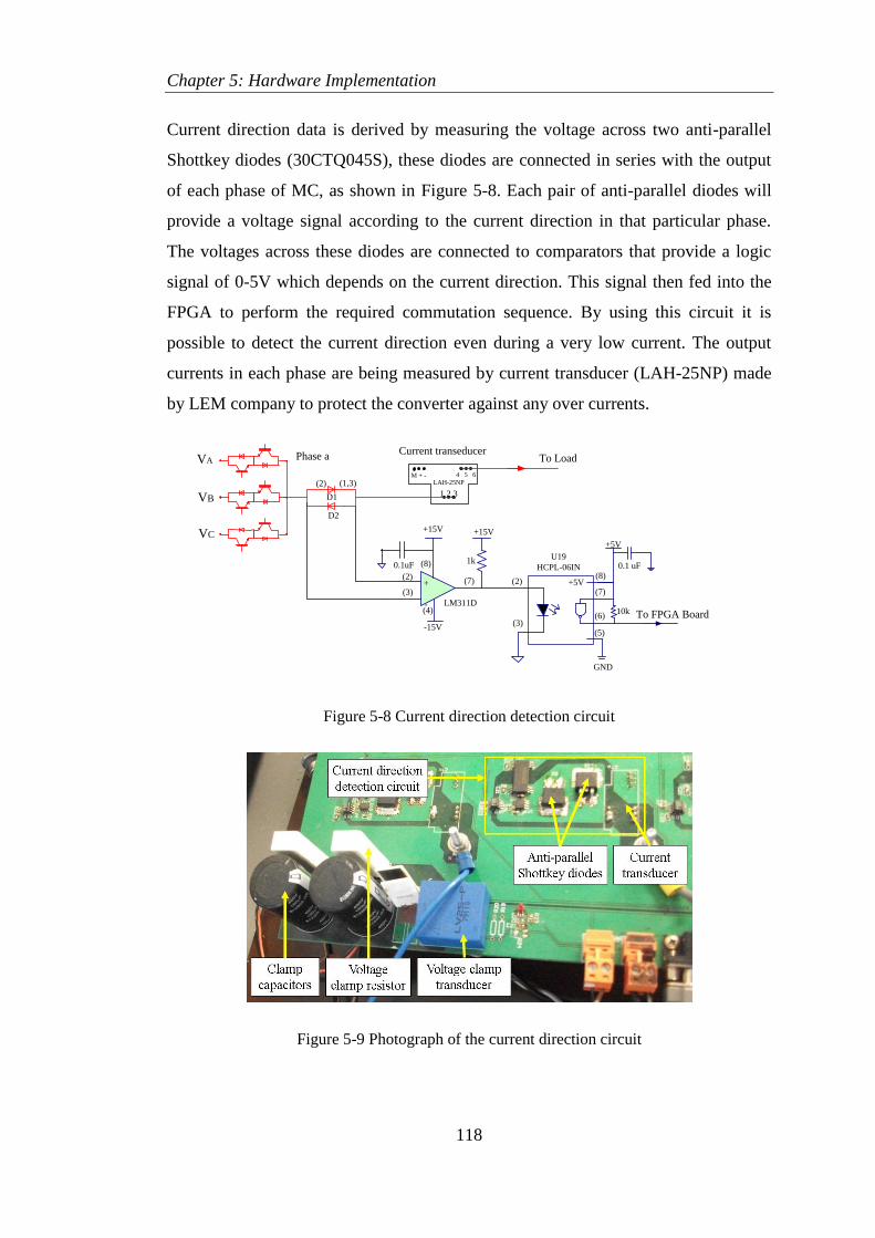
Chapter 5: Hardware Implementation
118
Current direction data is derived by measuring the voltage across two anti-parallel
Shottkey diodes (30CTQ045S), these diodes are connected in series with the output
of each phase of MC, as shown in Figure 5-8. Each pair of anti-parallel diodes will
provide a voltage signal according to the current direction in that particular phase.
The voltages across these diodes are connected to comparators that provide a logic
signal of 0-5V which depends on the current direction. This signal then fed into the
FPGA to perform the required commutation sequence. By using this circuit it is
possible to detect the current direction even during a very low current. The output
currents in each phase are being measured by current transducer (LAH-25NP) made
by LEM company to protect the converter against any over currents.
Phase a
D1
(1,3)(2)
D2
M + -LAH-25NP
U19
HCPL-06IN
LM311D
4 5 6
To Load
0.1uF1k
+15V
GND
+15V
(2)
(4)
(8)
(7)
+5V
(2)
(3)
(8)
(7)
(5)
0.1 uF
-15V
(3)+
-
(6)
+5V
10k To FPGA Board
1 2 3
Current transeducerVA
VB
VC
Figure 5-8 Current direction detection circuit
Figure 5-9 Photograph of the current direction circuit

Chapter 5: Hardware Implementation
119
5.7 Voltage clamp circuit
A clamp circuit is used as simple protection circuit to protect the converter against
any over voltage or currents that might occur during operation as shown in
Figure 5-9 and 5.10. It can be seen that the clamp circuit consists of two diode
rectifier with a clamp capacitor in parallel with bleed resistors. A 14 (8EWF12S) fast
recovery diodes are employed to construct the two rectifier circuits which are
mounted on the bottom layer of the power board. The fast recovery diodes are rated
at 1200V and 8A.
If there is a fault in the operation of the Matrix Converter such as commutation or
open circuit faults, the clamp circuit will provide a path for the currents and all the
energy can be transferred to the clamp capacitor and then dissipated in the parallel
resistor. A voltage transducer (LEM LV25-P) is used to measure the voltage across
the clamp capacitor. If the clamp voltage increases above a set level then the Matrix
Converter will be shut down by turning off the entire gate signal to the bi-directional
switches.
A proper selection of the clamp capacitor is important to protect the Matrix
Converter from dangerous overvoltage under fault conditions. The maximum energy
stored in the inductive load and the maximum peak to peak input supply voltage is
used to calculate the required clamp capacitor size.
The total energy stored in the three phase load is calculated as:
5-1
Where Q is the total energy stored in the load inductors L is the load inductance and
I is the RMS value of the load current [93].
The clamp capacitance can be calculated as
5-2
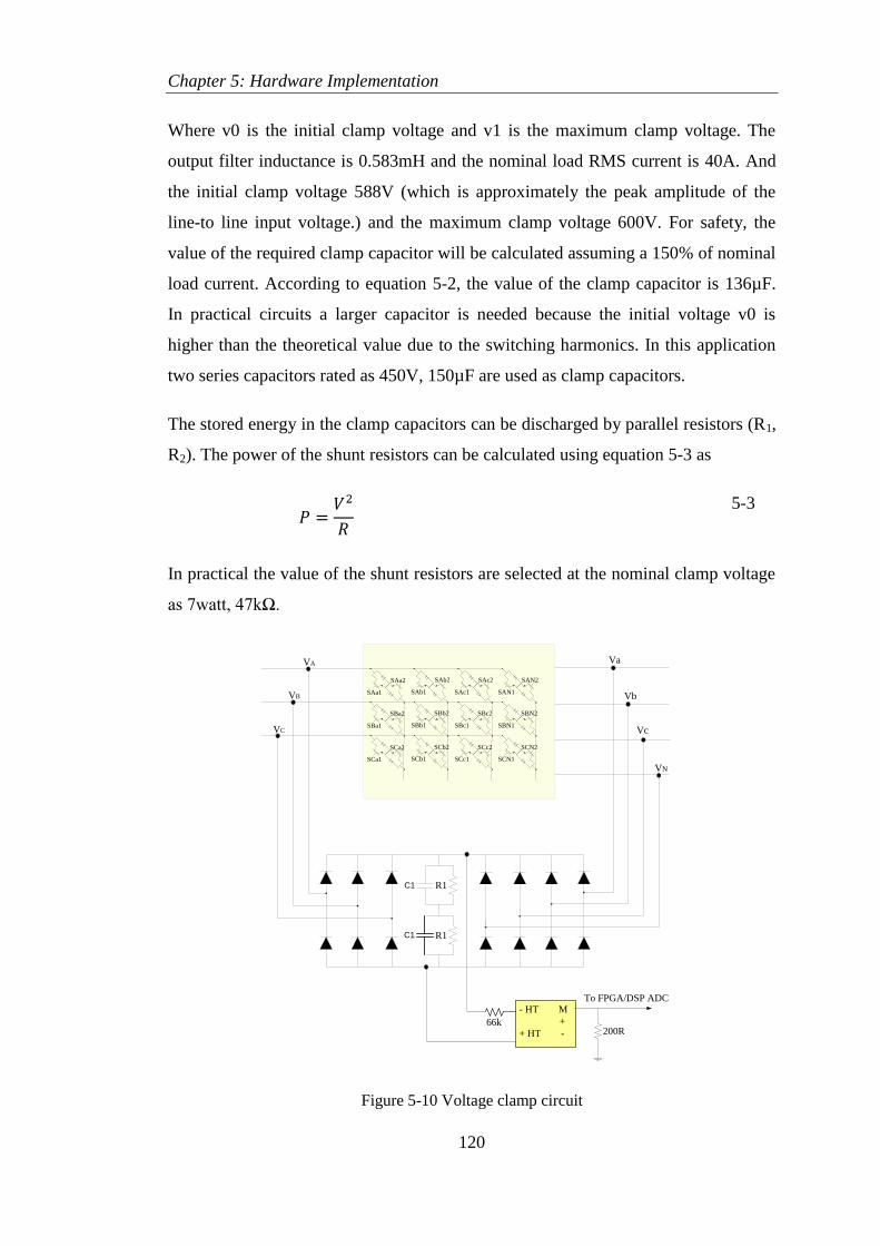
Chapter 5: Hardware Implementation
120
Where v0 is the initial clamp voltage and v1 is the maximum clamp voltage. The
output filter inductance is 0.583mH and the nominal load RMS current is 40A. And
the initial clamp voltage 588V (which is approximately the peak amplitude of the
line-to line input voltage.) and the maximum clamp voltage 600V. For safety, the
value of the required clamp capacitor will be calculated assuming a 150% of nominal
load current. According to equation 5-2, the value of the clamp capacitor is 136µF.
In practical circuits a larger capacitor is needed because the initial voltage v0 is
higher than the theoretical value due to the switching harmonics. In this application
two series capacitors rated as 450V, 150µF are used as clamp capacitors.
The stored energy in the clamp capacitors can be discharged by parallel resistors (R1,
R2). The power of the shunt resistors can be calculated using equation 5-3 as
5-3
In practical the value of the shunt resistors are selected at the nominal clamp voltage
as 7watt, 47kΩ.
R1C1
R1
VA
VB
VC
Va
Vb
Vc
VN
SAa2 SAb2 SAc2 SAN2
SBa2 SBb2 SBc2 SBN2
SCa2 SCb2 SCc2 SCN2
SCa1 SCb1 SCc1 SCN1
SBa1 SBb1 SBc1 SBN1
SAa1 SAb1 SAc1 SAN1
- HT M
+
+ HT -66k
200R
To FPGA/DSP ADC
C1
Figure 5-10 Voltage clamp circuit
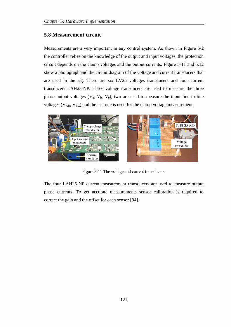
Chapter 5: Hardware Implementation
121
5.8 Measurement circuit
Measurements are a very important in any control system. As shown in Figure 5-2
the controller relies on the knowledge of the output and input voltages, the protection
circuit depends on the clamp voltages and the output currents. Figure 5-11 and 5.12
show a photograph and the circuit diagram of the voltage and current transducers that
are used in the rig. There are six LV25 voltages transducers and four current
transducers LAH25-NP. Three voltage transducers are used to measure the three
phase output voltages (Va, Vb, Vc), two are used to measure the input line to line
voltages (VAB, VBC) and the last one is used for the clamp voltage measurement.
Figure 5-11 The voltage and current transducers.
The four LAH25-NP current measurement transducers are used to measure output
phase currents. To get accurate measurements sensor calibration is required to
correct the gain and the offset for each sensor [94].
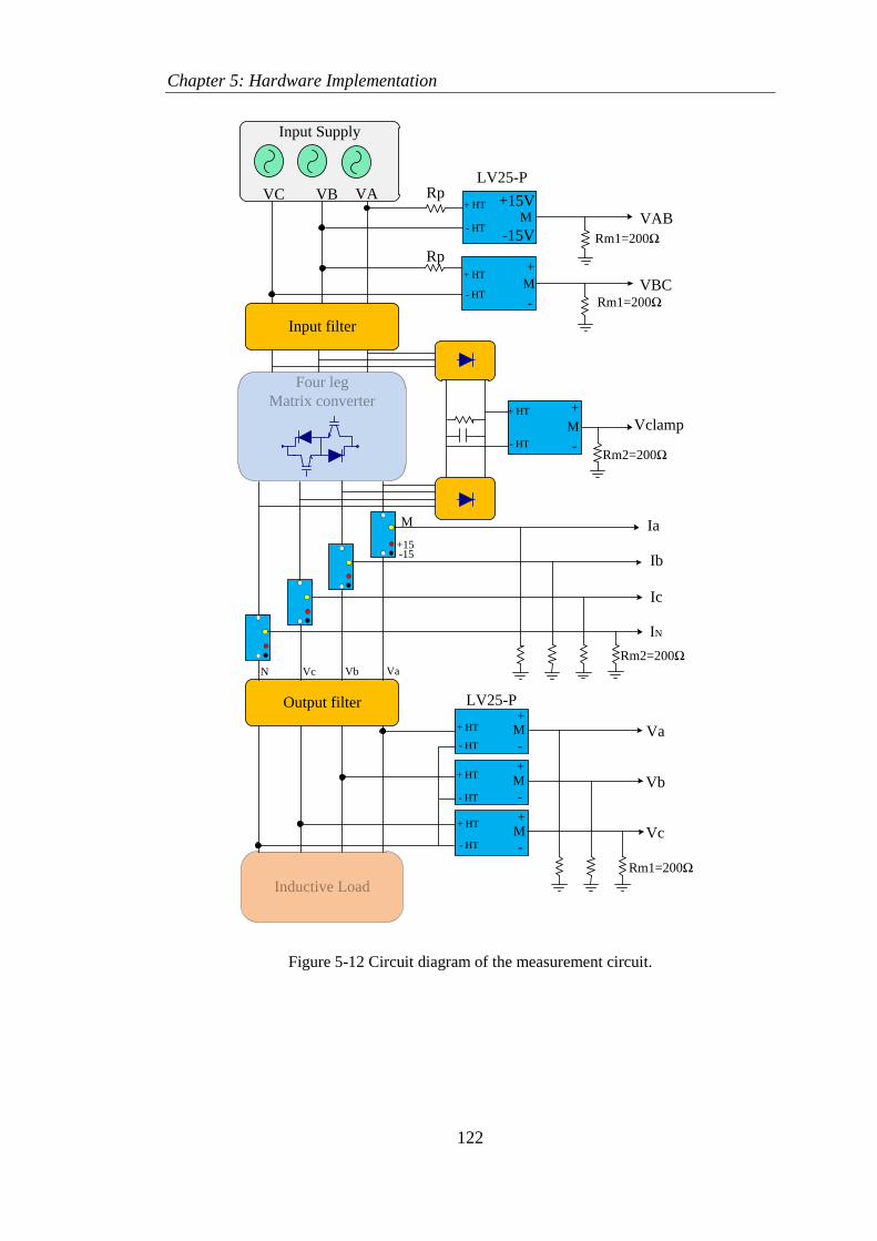
Chapter 5: Hardware Implementation
122
Output filter
Input filter
Input Supply
Four leg
Matrix converter
Rp
Rp
+ HT
- HTM VAB
+15V
-15V
+ HT
- HT
+
-
M VBC
Rm1=200Ω
Rm1=200Ω
VAVBVC
+15-15
M Ia
Rm2=200Ω
Ib
Ic
Inductive Load
+ HT
- HT
+
-
M Va
+ HT
- HT
+
-
M
+ HT
- HT
+
-
M
Rm1=200Ω
Vb
Vc
N Vc Vb Va
LV25-P
IN
+ HT
- HT
+
-
M
Rm2=200Ω
Vclamp
LV25-P
Figure 5-12 Circuit diagram of the measurement circuit.
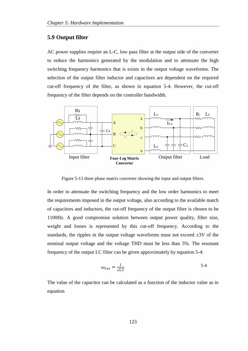
Chapter 5: Hardware Implementation
123
5.9 Output filter
AC power supplies require an L-C, low pass filter at the output side of the converter
to reduce the harmonics generated by the modulation and to attenuate the high
switching frequency harmonics that is exists in the output voltage waveforms. The
selection of the output filter inductor and capacitors are dependent on the required
cut-off frequency of the filter, as shown in equation 5-4. However, the cut-off
frequency of the filter depends on the controller bandwidth.
Co
LLRL
Io a
Lo
Ln
A
B
C
Ls
Rs
Cs
Input filter
a
b
c
n
Output filterFour-Leg Matrix
Converter
Load
Figure 5-13 three phase matrix converter showing the input and output filters.
In order to attenuate the switching frequency and the low order harmonics to meet
the requirements imposed in the output voltage, also according to the available match
of capacitors and inductors, the cut-off frequency of the output filter is chosen to be
1100Hz. A good compromise solution between output power quality, filter size,
weight and losses is represented by this cut-off frequency. According to the
standards, the ripples in the output voltage waveforms must not exceed ±3V of the
nominal output voltage and the voltage THD must be less than 5%. The resonant
frequency of the output LC filter can be given approximately by equation 5-4:
√ 5-4
The value of the capacitor can be calculated as a function of the inductor value as in
equation
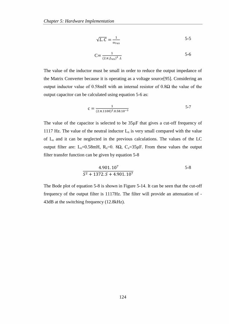
Chapter 5: Hardware Implementation
124
√
5-5
C
5-6
The value of the inductor must be small in order to reduce the output impedance of
the Matrix Converter because it is operating as a voltage source[95]. Considering an
output inductor value of 0.58mH with an internal resistor of 0.8Ω the value of the
output capacitor can be calculated using equation 5-6 as:
5-7
The value of the capacitor is selected to be 35µF that gives a cut-off frequency of
1117 Hz. The value of the neutral inductor Ln is very small compared with the value
of Lo and it can be neglected in the previous calculations. The values of the LC
output filter are: Lo=0.58mH, Ro=0. 8Ω, Co=35µF. From these values the output
filter transfer function can be given by equation 5-8
5-8
The Bode plot of equation 5-8 is shown in Figure 5-14. It can be seen that the cut-off
frequency of the output filter is 1117Hz. The filter will provide an attenuation of -
43dB at the switching frequency (12.8kHz).
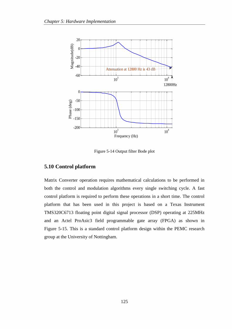
Chapter 5: Hardware Implementation
125
Figure 5-14 Output filter Bode plot
5.10 Control platform
Matrix Converter operation requires mathematical calculations to be performed in
both the control and modulation algorithms every single switching cycle. A fast
control platform is required to perform these operations in a short time. The control
platform that has been used in this project is based on a Texas Instrument
TMS320C6713 floating point digital signal processor (DSP) operating at 225MHz
and an Actel ProAsic3 field programmable gate array (FPGA) as shown in
Figure 5-15. This is a standard control platform design within the PEMC research
group at the University of Nottingham.
103
104
-60
-40
-20
0
20
Mag
nit
ud
e(d
B)
103
104
-200
-150
-100
-50
0
Frequency (Hz)
Ph
ase
(deg
)Attenuation at 12800 Hz is 43 dB
12800Hz
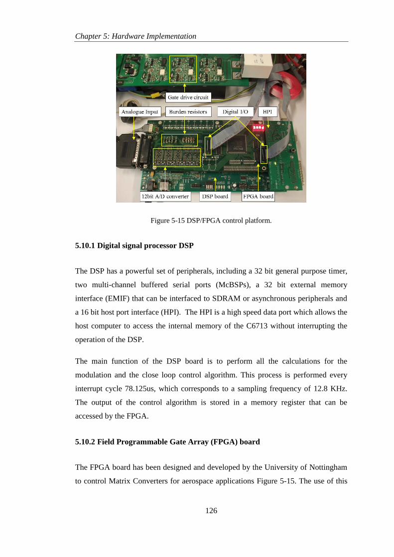
Chapter 5: Hardware Implementation
126
Figure 5-15 DSP/FPGA control platform.
5.10.1 Digital signal processor DSP
The DSP has a powerful set of peripherals, including a 32 bit general purpose timer,
two multi-channel buffered serial ports (McBSPs), a 32 bit external memory
interface (EMIF) that can be interfaced to SDRAM or asynchronous peripherals and
a 16 bit host port interface (HPI). The HPI is a high speed data port which allows the
host computer to access the internal memory of the C6713 without interrupting the
operation of the DSP.
The main function of the DSP board is to perform all the calculations for the
modulation and the close loop control algorithm. This process is performed every
interrupt cycle 78.125us, which corresponds to a sampling frequency of 12.8 KHz.
The output of the control algorithm is stored in a memory register that can be
accessed by the FPGA.
5.10.2 Field Programmable Gate Array (FPGA) board
The FPGA board has been designed and developed by the University of Nottingham
to control Matrix Converters for aerospace applications Figure 5-15. The use of this
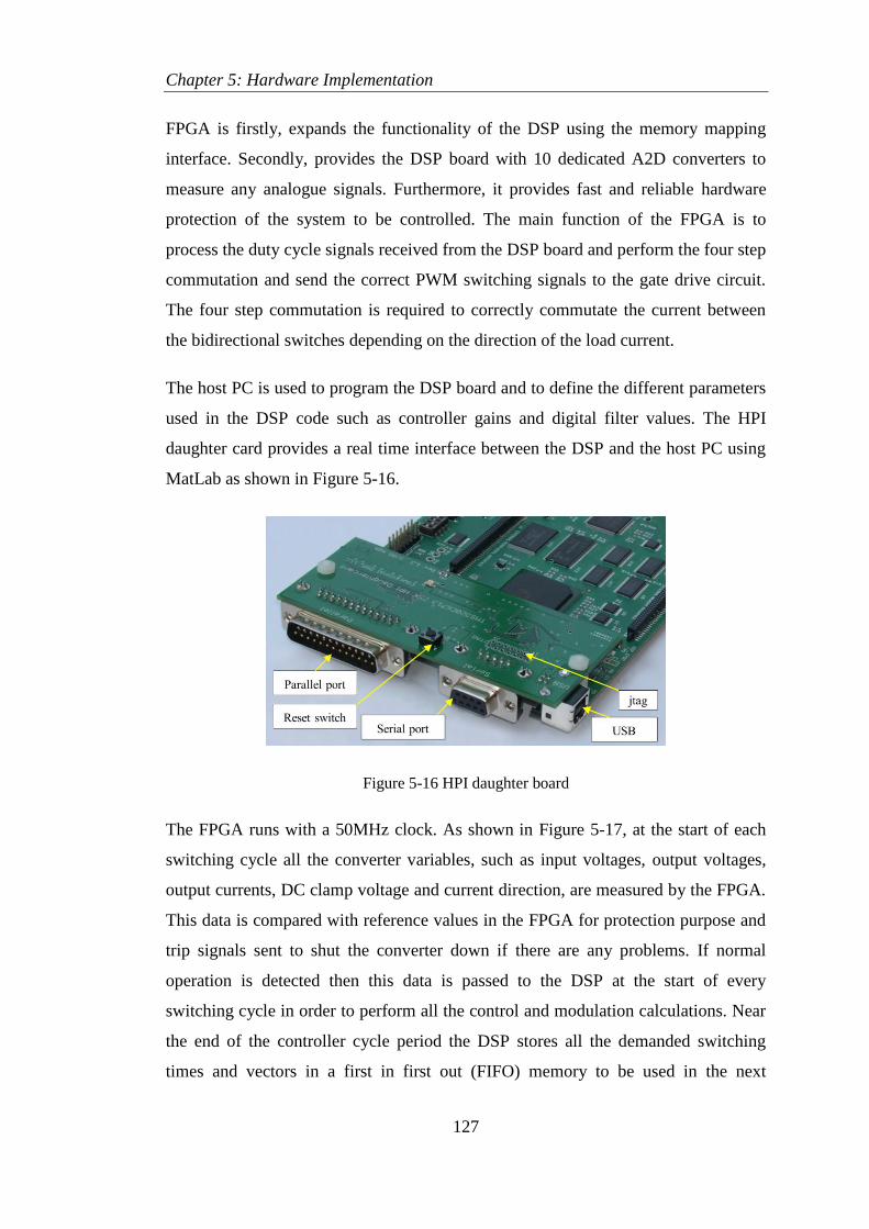
Chapter 5: Hardware Implementation
127
FPGA is firstly, expands the functionality of the DSP using the memory mapping
interface. Secondly, provides the DSP board with 10 dedicated A2D converters to
measure any analogue signals. Furthermore, it provides fast and reliable hardware
protection of the system to be controlled. The main function of the FPGA is to
process the duty cycle signals received from the DSP board and perform the four step
commutation and send the correct PWM switching signals to the gate drive circuit.
The four step commutation is required to correctly commutate the current between
the bidirectional switches depending on the direction of the load current.
The host PC is used to program the DSP board and to define the different parameters
used in the DSP code such as controller gains and digital filter values. The HPI
daughter card provides a real time interface between the DSP and the host PC using
MatLab as shown in Figure 5-16.
Figure 5-16 HPI daughter board
The FPGA runs with a 50MHz clock. As shown in Figure 5-17, at the start of each
switching cycle all the converter variables, such as input voltages, output voltages,
output currents, DC clamp voltage and current direction, are measured by the FPGA.
This data is compared with reference values in the FPGA for protection purpose and
trip signals sent to shut the converter down if there are any problems. If normal
operation is detected then this data is passed to the DSP at the start of every
switching cycle in order to perform all the control and modulation calculations. Near
the end of the controller cycle period the DSP stores all the demanded switching
times and vectors in a first in first out (FIFO) memory to be used in the next
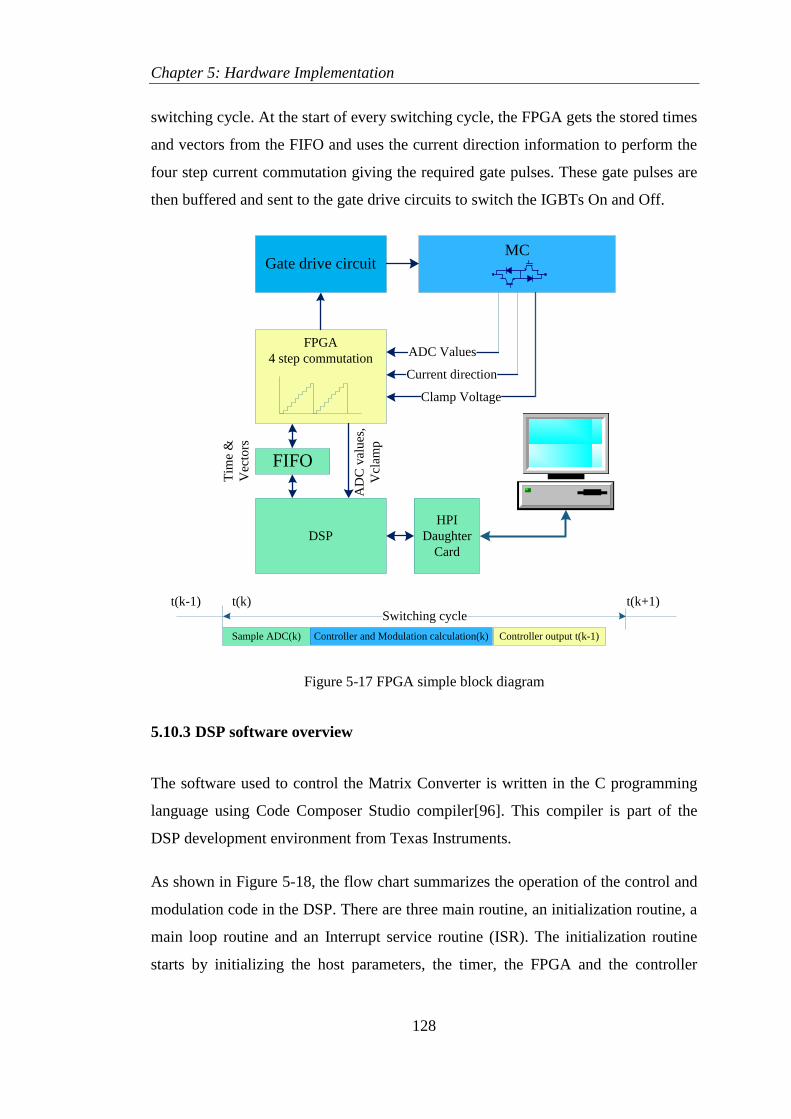
Chapter 5: Hardware Implementation
128
switching cycle. At the start of every switching cycle, the FPGA gets the stored times
and vectors from the FIFO and uses the current direction information to perform the
four step current commutation giving the required gate pulses. These gate pulses are
then buffered and sent to the gate drive circuits to switch the IGBTs On and Off.
Tim
e &
Vec
tors
DSP
FPGA
4 step commutation
Current direction
Clamp Voltage
Gate drive circuitMC
FIFO
HPI
Daughter
Card
AD
C v
alu
es,
Vcl
amp
ADC Values
t(k) Switching cycle
t(k+1)t(k-1)
Sample ADC(k) Controller and Modulation calculation(k) Controller output t(k-1)
Figure 5-17 FPGA simple block diagram
5.10.3 DSP software overview
The software used to control the Matrix Converter is written in the C programming
language using Code Composer Studio compiler[96]. This compiler is part of the
DSP development environment from Texas Instruments.
As shown in Figure 5-18, the flow chart summarizes the operation of the control and
modulation code in the DSP. There are three main routine, an initialization routine, a
main loop routine and an Interrupt service routine (ISR). The initialization routine
starts by initializing the host parameters, the timer, the FPGA and the controller

Chapter 5: Hardware Implementation
129
parameters. Next, the program enters to the main loop in which there is an endless
loop running. In this endless loop the program keeps processing and displaying a
massage signal, that describes the health condition of the converter, until an interrupt
signal from the FPGA is detected. Once the interrupt signal has been detected the
program jumps to the Interrupt Service Routine (ISR) loop. In the ISR, the program
starts by resetting the timer and send a signal to the FPGA to start the ADC process.
The ISR then waits for a handshaking signal from the FPGA to acknowledge that the
ADC conversion process ended and the transducer’s data are ready in the ADC
buffer. Next, the software protection code will compare the measured voltages and
the currents with respect to pre-set trip values and a command signal will be sent to
shut the converter down if there are any problems.
If there are no faults, the program will process the control subroutine and calculate
the control commands based on both second order controller and repetitive
controllers. After that, the program calculates the duty cycles using Venturini
modulation, and converts them to time and vectors. Finally, the program places the
calculated times and the vectors to the FPGA first in first out (FIFO) register to be
used in the next sampling period as shown in Figure 5-18.
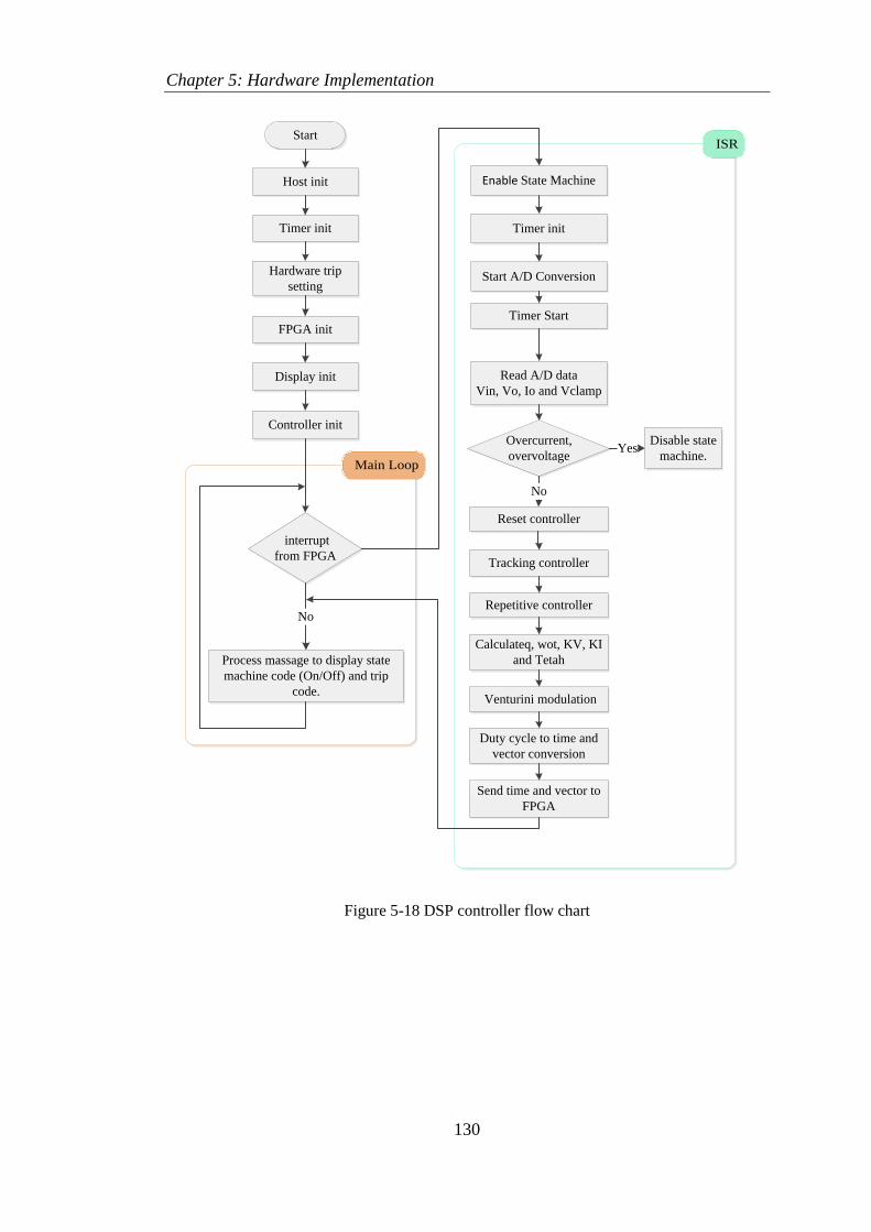
Chapter 5: Hardware Implementation
130
ISR
Timer init
Start A/D Conversion
Timer Start
Read A/D data
Vin, Vo, Io and Vclamp
Overcurrent,
overvoltage
Disable state
machine.Yes
Reset controller
No
Tracking controller
Repetitive controller
Calculateq, wot, KV, KI
and Tetah
Venturini modulation
Duty cycle to time and
vector conversion
Send time and vector to
FPGA
Main Loop
Start
Host init
Timer init
Hardware trip
setting
FPGA init
Display init
Controller init
interrupt
from FPGA
Process massage to display state
machine code (On/Off) and trip
code.
No
Enable State Machine
Figure 5-18 DSP controller flow chart

Chapter 5: Hardware Implementation
131
5.11 Summery
The experimental setup and the implementation of a 7.5KW four-leg Matrix
Converter laboratory prototype have been presented in this chapter. The design,
construction and assembly have been described in details. The four-leg Matrix
Converter prototype consists of the input filter, the power modules, the gate drive
circuit, current direction circuit, voltage clamp circuit, measurement circuit, the
output filter and the control platform. The explanation of the functionality and
construction of these components has been given.
The next chapter will present the experimental results for the four-leg Matrix
Converter prototype for a range of load conditions, and transients to verify the
effectiveness of the proposed controller and to enable the validation of the simulation
results.

Chapter 6 Experimental Results
132
Chapter 6 Experimental Results
6.1 Introduction
The initial design of the prototype of the four-leg Matrix Converter prototype has
been investigated through a series of simulation tests using SABER and MatLab
simulation packages as showed in chapter 4. The implementation and the setup of the
four-leg Matrix Converter prototype for GPU application has been presented in
chapter 5.
In this chapter experimental results of four-leg Matrix Converter using repetitive and
second order controller is presented to demonstrate the effectiveness of the proposed
controller, and to validate the simulation results presented in chapter 4. In order to do
that a series of experimental tests have been done to test the converter response for
different loading.
The chapter starts by introducing the system parameters. Then, the experimental
results of the four-leg Matrix Converter are presented for a balanced, an unbalanced
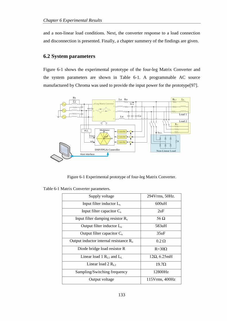
Chapter 6 Experimental Results
133
and a non-linear load conditions. Next, the converter response to a load connection
and disconnection is presented. Finally, a chapter summery of the findings are given.
6.2 System parameters
Figure 6-1 shows the experimental prototype of the four-leg Matrix Converter and
the system parameters are shown in Table 6-1. A programmable AC source
manufactured by Chroma was used to provide the input power for the prototype[97].
Lo
Ln Co
LLRL1
Io a
Controller
Controller
ControllerModulator
Vm
Ls
Rs
PLL
A
B
C
a
b
c
N
Vmax
wit
DSP/FPGA Controller
R
Non-Linear Load
4 Leg Matrix Converter
Ro
Cs
INLL
RL2
Load 1
Load 2
Host interface
Figure 6-1 Experimental prototype of four-leg Matrix Converter.
Table 6-1 Matrix Converter parameters.
Supply voltage 294Vrms, 50Hz.
Input filter inductor Ls 600uH
Input filter capacitor Cs 2uF
Input filter damping resistor Rs 56 Ω
Output filter inductor Lo 583uH
Output filter capacitor Co 35uF
Output inductor internal resistance Ro 0.2
Diode bridge load resistor R R=30
Linear load 1 RL1 and LL 12Ω, 6.25mH
Linear load 2 RL2 19.7
Sampling/Switching frequency 12800Hz
Output voltage 115Vrms, 400Hz
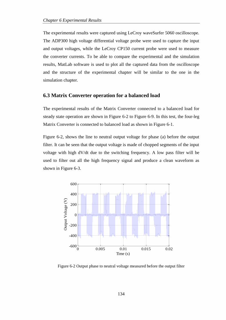
Chapter 6 Experimental Results
134
The experimental results were captured using LeCroy waveSurfer 5060 oscilloscope.
The ADP300 high voltage differential voltage probe were used to capture the input
and output voltages, while the LeCroy CP150 current probe were used to measure
the converter currents. To be able to compare the experimental and the simulation
results, MatLab software is used to plot all the captured data from the oscilloscope
and the structure of the experimental chapter will be similar to the one in the
simulation chapter.
6.3 Matrix Converter operation for a balanced load
The experimental results of the Matrix Converter connected to a balanced load for
steady state operation are shown in Figure 6-2 to Figure 6-9. In this test, the four-leg
Matrix Converter is connected to balanced load as shown in Figure 6-1.
Figure 6-2, shows the line to neutral output voltage for phase (a) before the output
filter. It can be seen that the output voltage is made of chopped segments of the input
voltage with high dV/dt due to the switching frequency. A low pass filter will be
used to filter out all the high frequency signal and produce a clean waveform as
shown in Figure 6-3.
Figure 6-2 Output phase to neutral voltage measured before the output filter
0 0.005 0.01 0.015 0.02-600
-400
-200
0
200
400
600
Time (s)
Ou
tpu
t V
olt
ag
e (
V)
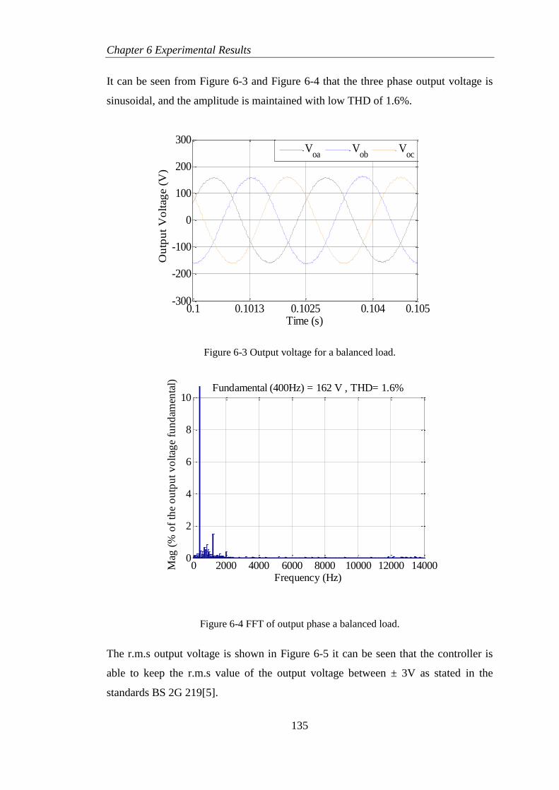
Chapter 6 Experimental Results
135
It can be seen from Figure 6-3 and Figure 6-4 that the three phase output voltage is
sinusoidal, and the amplitude is maintained with low THD of 1.6%.
Figure 6-3 Output voltage for a balanced load.
Figure 6-4 FFT of output phase a balanced load.
The r.m.s output voltage is shown in Figure 6-5 it can be seen that the controller is
able to keep the r.m.s value of the output voltage between ± 3V as stated in the
standards BS 2G 219[5].
0.1 0.1013 0.1025 0.104 0.105-300
-200
-100
0
100
200
300
Time (s)
Ou
tpu
t V
olt
age
(V)
V
oaV
obV
oc
0 2000 4000 6000 8000 10000 12000 140000
2
4
6
8
10
Frequency (Hz)
Fundamental (400Hz) = 162 V , THD= 1.6%
Mag
(%
of
the
ou
tpu
t v
olt
age
fun
dam
enta
l)
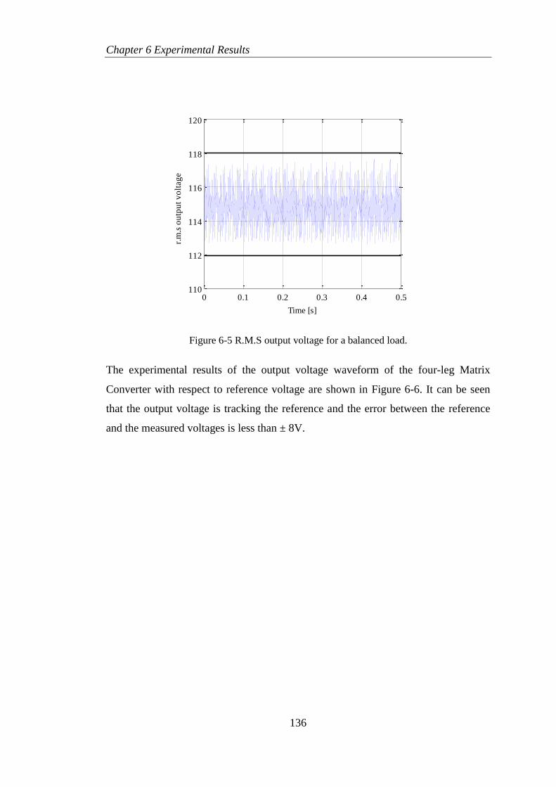
Chapter 6 Experimental Results
136
Figure 6-5 R.M.S output voltage for a balanced load.
The experimental results of the output voltage waveform of the four-leg Matrix
Converter with respect to reference voltage are shown in Figure 6-6. It can be seen
that the output voltage is tracking the reference and the error between the reference
and the measured voltages is less than ± 8V.
0 0.1 0.2 0.3 0.4 0.5110
112
114
116
118
120
Time [s]
r.m
.s o
utp
ut
vo
ltag
e
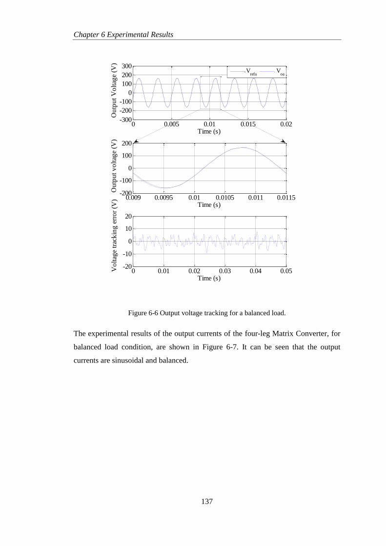
Chapter 6 Experimental Results
137
Figure 6-6 Output voltage tracking for a balanced load.
The experimental results of the output currents of the four-leg Matrix Converter, for
balanced load condition, are shown in Figure 6-7. It can be seen that the output
currents are sinusoidal and balanced.
0 0.005 0.01 0.015 0.02-300
-200
-100
0
100
200
300
Time (s)
Ou
tpu
t V
olt
age
(V)
V
refaV
oa
0.009 0.0095 0.01 0.0105 0.011 0.0115-200
-100
0
100
200
Time (s)
Ou
tpu
t v
olt
age
(V)
0 0.01 0.02 0.03 0.04 0.05-20
-10
0
10
20
Time (s)
Vo
ltag
e tr
ack
ing
err
or
(V)
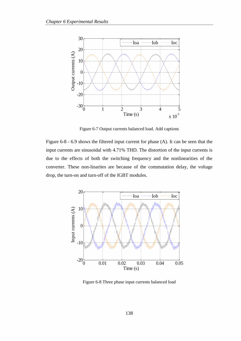
Chapter 6 Experimental Results
138
Figure 6-7 Output currents balanced load. Add captions
Figure 6-8 - 6.9 shows the filtered input current for phase (A). It can be seen that the
input currents are sinusoidal with 4.71% THD. The distortion of the input currents is
due to the effects of both the switching frequency and the nonlinearities of the
converter. These non-linarites are because of the commutation delay, the voltage
drop, the turn-on and turn-off of the IGBT modules.
Figure 6-8 Three phase input currents balanced load
0 1 2 3 4 5
x 10-3
-30
-20
-10
0
10
20
30
Time (s)
Ou
tpu
t cu
rren
ts (
A)
Ioa Iob Ioc
0 0.01 0.02 0.03 0.04 0.05-20
-10
0
10
20
Time (s)
Inp
ut
curr
ents
(A
)
Ioa Iob Ioc

Chapter 6 Experimental Results
139
Figure 6-9 Input current spectra of phase A, for a balanced load condition.
6.4 Unbalanced load conditions
In this section the experimental results of the four-leg Matrix Converter is presented
to demonstrate the ability of the proposed controller to regulate the output voltage of
the converter under unbalanced loading.
For an unbalanced load conditions, negative and zero sequence components will flow
in the neutral wire of a three phase four wire systems. As a result of the unbalance
the output voltages will be distorted. It is the controller responsibility to ensure that
the output voltages will be supplied with the minimum of distortion. In this section
the experimental results of the four-leg Matrix Converter are shown to test the
proposed controller’s ability to regulate the output voltage under unbalanced loading.
The use of the repetitive and second order controller in ABC reference frame has the
privilege to control the output voltage of the four-leg Matrix Converter individually.
For this test, the balanced load1 was replaced by unbalanced load as bellow as shown
in Figure 6-10:
0 2000 4000 6000 8000 10000 12000 140000
2
4
6
8
10
Frequency (Hz)
Fundamental (50Hz) = 12.53 A , THD= 4.71%
Mag
(%
of
the
inp
ut
curr
ent
fun
dam
enta
l)
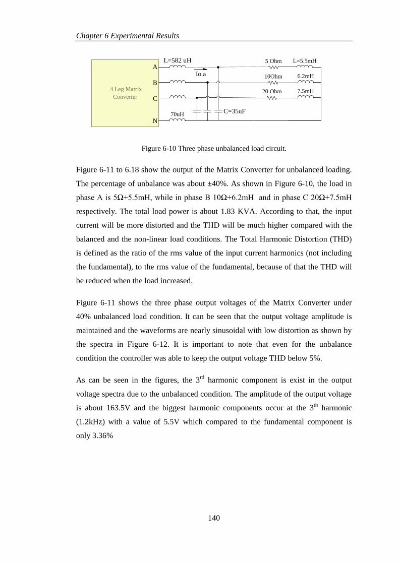
Chapter 6 Experimental Results
140
C=35uF
10Ohm
L=5.5mH
6.2mH
7.5mH
5 Ohm
Io a
L=582 uH
70uH
4 Leg Matrix
Converter20 Ohm
A
B
C
N
Figure 6-10 Three phase unbalanced load circuit.
Figure 6-11 to 6.18 show the output of the Matrix Converter for unbalanced loading.
The percentage of unbalance was about ±40%. As shown in Figure 6-10, the load in
phase A is 5Ω+5.5mH, while in phase B 10Ω+6.2mH and in phase C 20Ω+7.5mH
respectively. The total load power is about 1.83 KVA. According to that, the input
current will be more distorted and the THD will be much higher compared with the
balanced and the non-linear load conditions. The Total Harmonic Distortion (THD)
is defined as the ratio of the rms value of the input current harmonics (not including
the fundamental), to the rms value of the fundamental, because of that the THD will
be reduced when the load increased.
Figure 6-11 shows the three phase output voltages of the Matrix Converter under
40% unbalanced load condition. It can be seen that the output voltage amplitude is
maintained and the waveforms are nearly sinusoidal with low distortion as shown by
the spectra in Figure 6-12. It is important to note that even for the unbalance
condition the controller was able to keep the output voltage THD below 5%.
As can be seen in the figures, the 3rd
harmonic component is exist in the output
voltage spectra due to the unbalanced condition. The amplitude of the output voltage
is about 163.5V and the biggest harmonic components occur at the 3th
harmonic
(1.2kHz) with a value of 5.5V which compared to the fundamental component is
only 3.36%
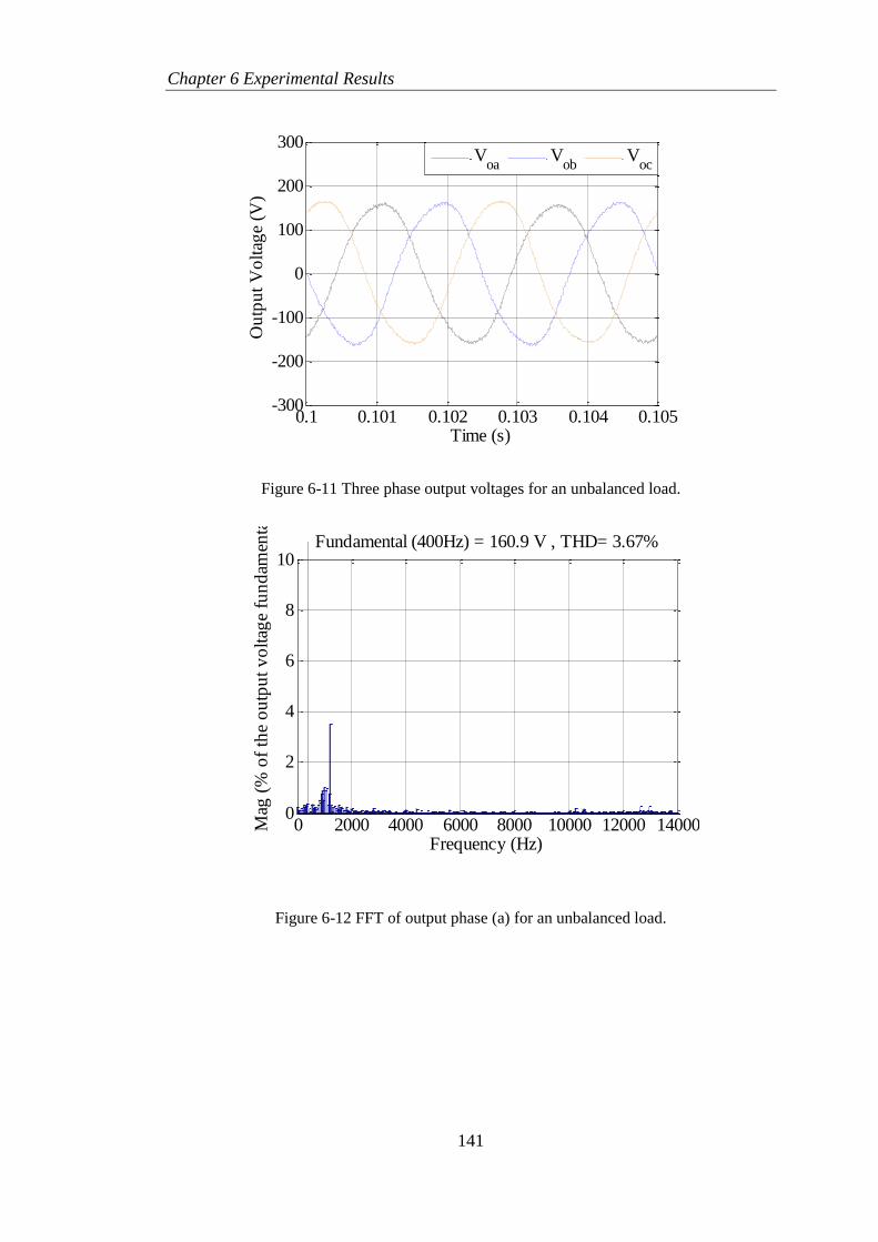
Chapter 6 Experimental Results
141
Figure 6-11 Three phase output voltages for an unbalanced load.
Figure 6-12 FFT of output phase (a) for an unbalanced load.
0.1 0.101 0.102 0.103 0.104 0.105-300
-200
-100
0
100
200
300
Time (s)
Ou
tpu
t V
olt
age
(V)
V
oaV
obV
oc
0 2000 4000 6000 8000 10000 12000 140000
2
4
6
8
10
Frequency (Hz)
Fundamental (400Hz) = 160.9 V , THD= 3.67%
Mag
(%
of
the
ou
tpu
t v
olt
age
fun
dam
enta
l)
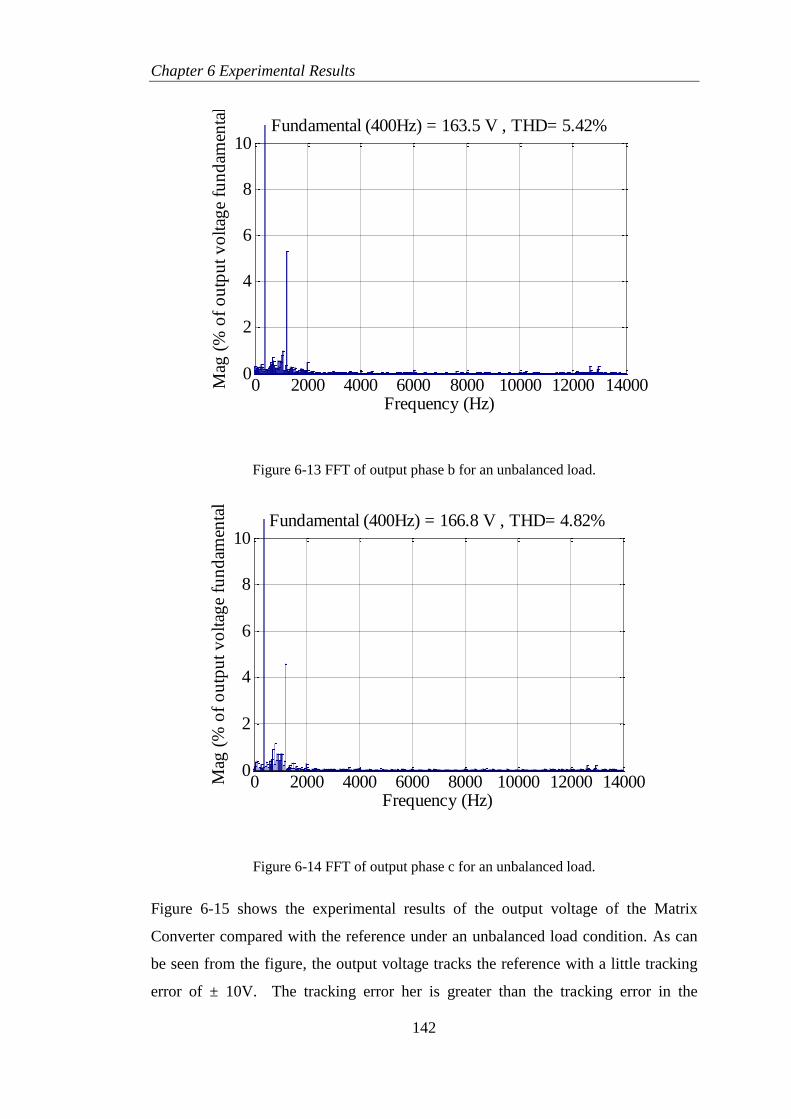
Chapter 6 Experimental Results
142
Figure 6-13 FFT of output phase b for an unbalanced load.
Figure 6-14 FFT of output phase c for an unbalanced load.
Figure 6-15 shows the experimental results of the output voltage of the Matrix
Converter compared with the reference under an unbalanced load condition. As can
be seen from the figure, the output voltage tracks the reference with a little tracking
error of ± 10V. The tracking error her is greater than the tracking error in the
0 2000 4000 6000 8000 10000 12000 140000
2
4
6
8
10
Frequency (Hz)
Fundamental (400Hz) = 163.5 V , THD= 5.42%
Mag
(%
of
ou
tpu
t v
olt
age
fun
dam
enta
l)
0 2000 4000 6000 8000 10000 12000 140000
2
4
6
8
10
Frequency (Hz)
Fundamental (400Hz) = 166.8 V , THD= 4.82%
Mag
(%
of
ou
tpu
t v
olt
age
fun
dam
enta
l)
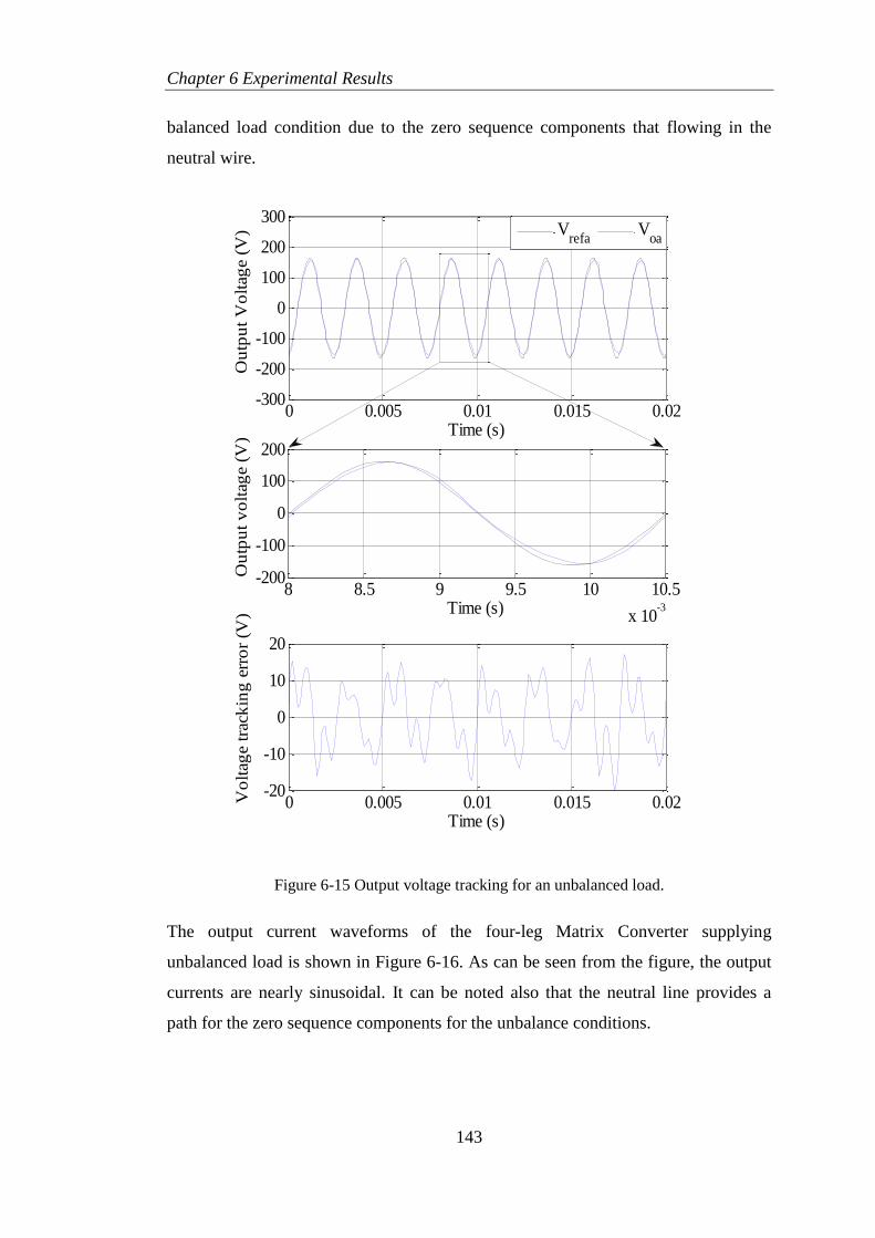
Chapter 6 Experimental Results
143
balanced load condition due to the zero sequence components that flowing in the
neutral wire.
Figure 6-15 Output voltage tracking for an unbalanced load.
The output current waveforms of the four-leg Matrix Converter supplying
unbalanced load is shown in Figure 6-16. As can be seen from the figure, the output
currents are nearly sinusoidal. It can be noted also that the neutral line provides a
path for the zero sequence components for the unbalance conditions.
0 0.005 0.01 0.015 0.02-300
-200
-100
0
100
200
300
Time (s)
Ou
tpu
t V
olt
age
(V)
V
refaV
oa
8 8.5 9 9.5 10 10.5
x 10-3
-200
-100
0
100
200
Time (s)
Ou
tpu
t v
olt
age
(V)
0 0.005 0.01 0.015 0.02-20
-10
0
10
20
Time (s)
Vo
ltag
e tr
ack
ing
err
or
(V)
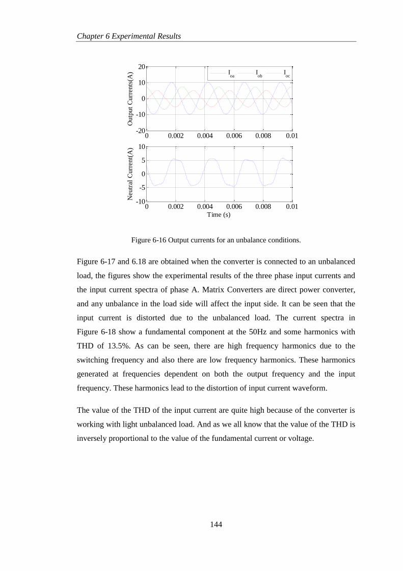
Chapter 6 Experimental Results
144
Figure 6-16 Output currents for an unbalance conditions.
Figure 6-17 and 6.18 are obtained when the converter is connected to an unbalanced
load, the figures show the experimental results of the three phase input currents and
the input current spectra of phase A. Matrix Converters are direct power converter,
and any unbalance in the load side will affect the input side. It can be seen that the
input current is distorted due to the unbalanced load. The current spectra in
Figure 6-18 show a fundamental component at the 50Hz and some harmonics with
THD of 13.5%. As can be seen, there are high frequency harmonics due to the
switching frequency and also there are low frequency harmonics. These harmonics
generated at frequencies dependent on both the output frequency and the input
frequency. These harmonics lead to the distortion of input current waveform.
The value of the THD of the input current are quite high because of the converter is
working with light unbalanced load. And as we all know that the value of the THD is
inversely proportional to the value of the fundamental current or voltage.
0 0.002 0.004 0.006 0.008 0.01-20
-10
0
10
20
Ou
tpu
t C
urr
ents
(A)
0 0.002 0.004 0.006 0.008 0.01-10
-5
0
5
10
Time (s)
Neu
tral
Cu
rren
t(A
)
Ioa
Iob
Ioc
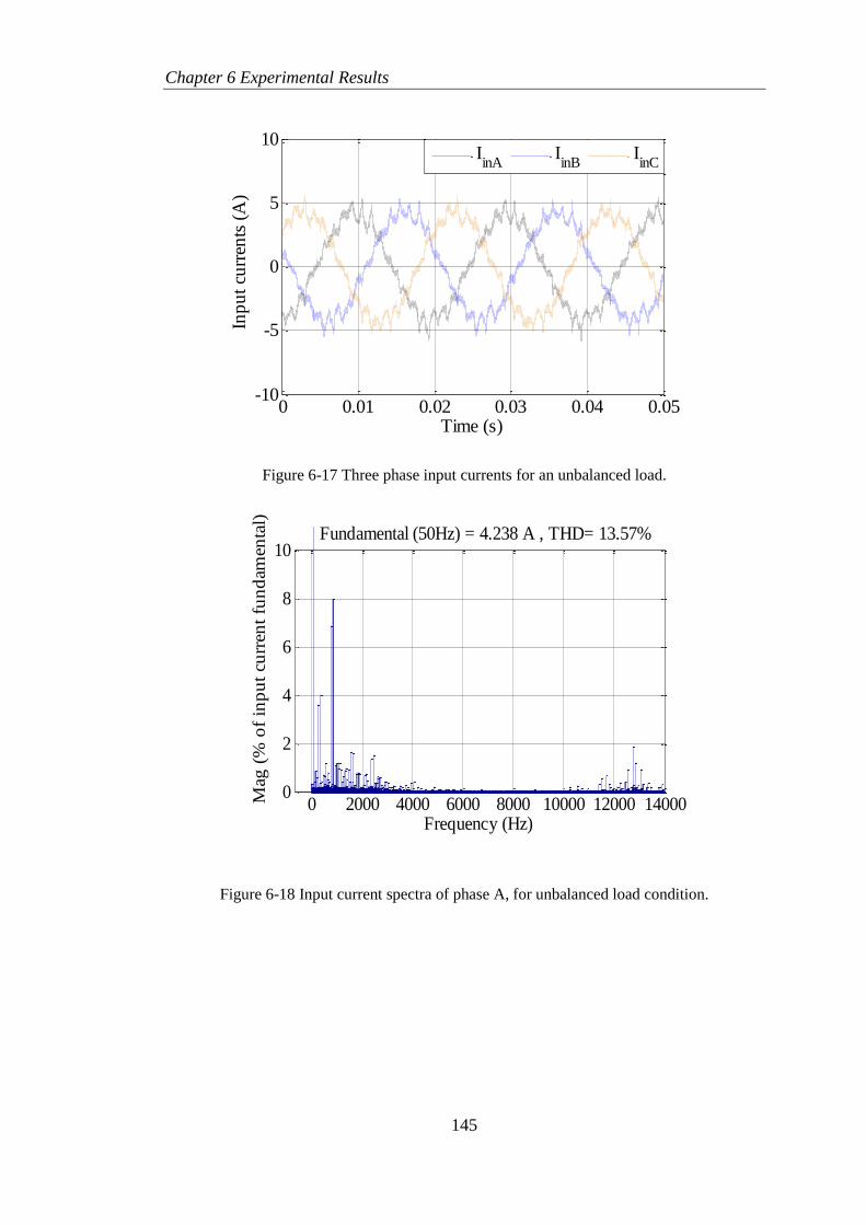
Chapter 6 Experimental Results
145
Figure 6-17 Three phase input currents for an unbalanced load.
Figure 6-18 Input current spectra of phase A, for unbalanced load condition.
0 0.01 0.02 0.03 0.04 0.05-10
-5
0
5
10
Time (s)
Inp
ut
curr
ents
(A
)
IinA
IinB
IinC
0 2000 4000 6000 8000 10000 12000 140000
2
4
6
8
10
Frequency (Hz)
Fundamental (50Hz) = 4.238 A , THD= 13.57%
Mag
(%
of
inp
ut
curr
ent
fun
dam
enta
l)
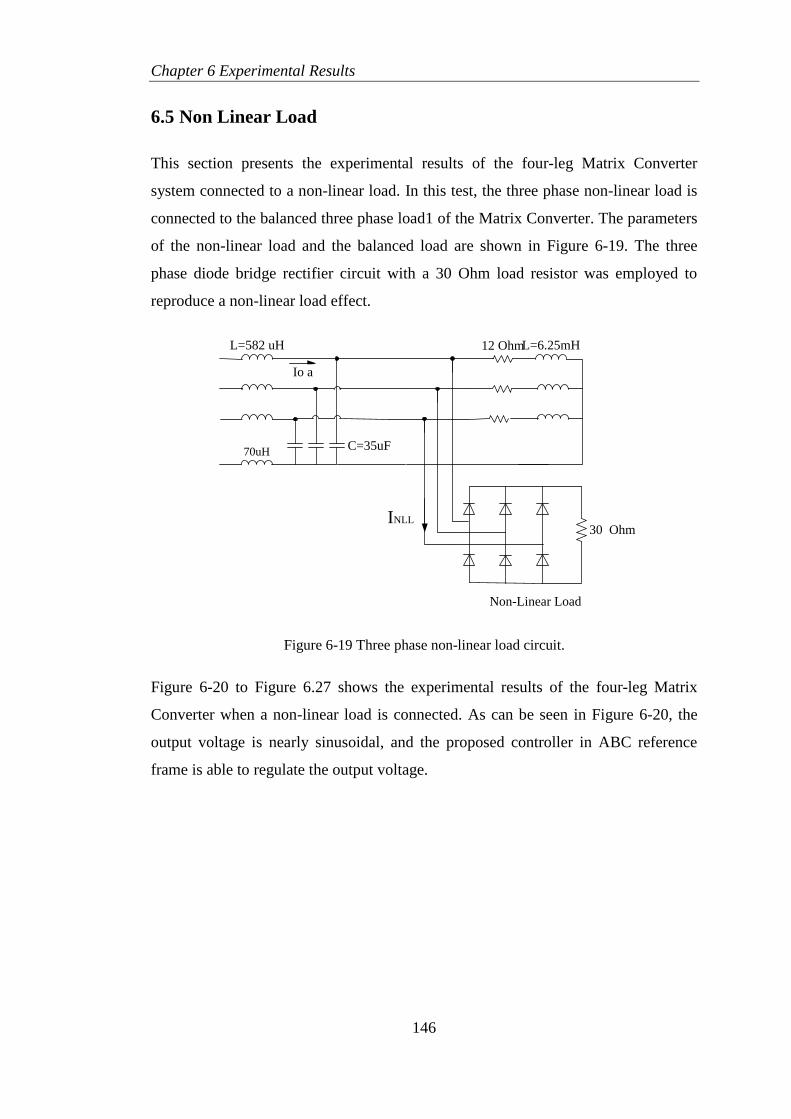
Chapter 6 Experimental Results
146
6.5 Non Linear Load
This section presents the experimental results of the four-leg Matrix Converter
system connected to a non-linear load. In this test, the three phase non-linear load is
connected to the balanced three phase load1 of the Matrix Converter. The parameters
of the non-linear load and the balanced load are shown in Figure 6-19. The three
phase diode bridge rectifier circuit with a 30 Ohm load resistor was employed to
reproduce a non-linear load effect.
C=35uF
L=6.25mH12 Ohm
Io a
30 Ohm
Non-Linear Load
L=582 uH
70uH
INLL
Figure 6-19 Three phase non-linear load circuit.
Figure 6-20 to Figure 6.27 shows the experimental results of the four-leg Matrix
Converter when a non-linear load is connected. As can be seen in Figure 6-20, the
output voltage is nearly sinusoidal, and the proposed controller in ABC reference
frame is able to regulate the output voltage.
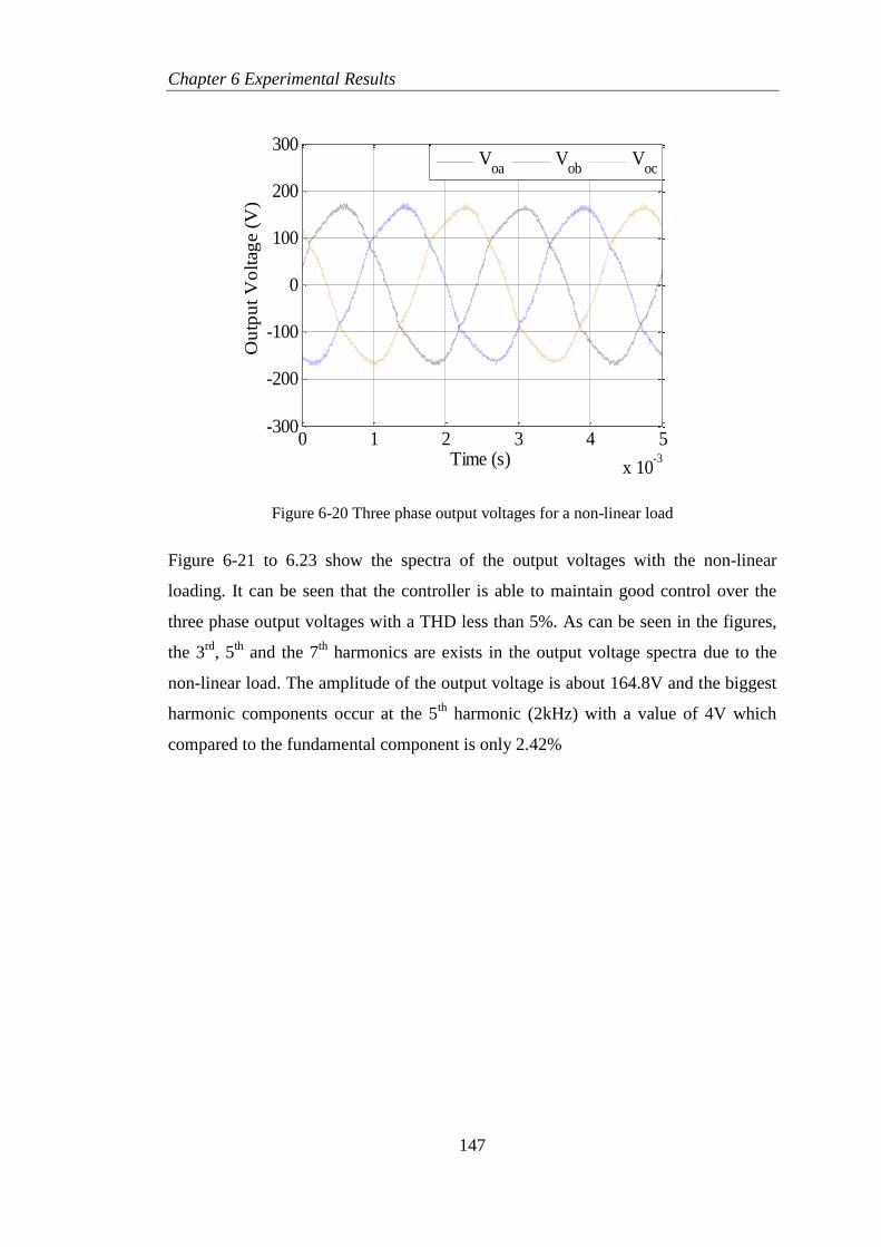
Chapter 6 Experimental Results
147
Figure 6-20 Three phase output voltages for a non-linear load
Figure 6-21 to 6.23 show the spectra of the output voltages with the non-linear
loading. It can be seen that the controller is able to maintain good control over the
three phase output voltages with a THD less than 5%. As can be seen in the figures,
the 3rd
, 5th
and the 7th
harmonics are exists in the output voltage spectra due to the
non-linear load. The amplitude of the output voltage is about 164.8V and the biggest
harmonic components occur at the 5th
harmonic (2kHz) with a value of 4V which
compared to the fundamental component is only 2.42%
0 1 2 3 4 5
x 10-3
-300
-200
-100
0
100
200
300
Time (s)
Ou
tpu
t V
olt
age
(V)
V
oaV
obV
oc
Chapter 6 Experimental Results
148
Figure 6-21 Output voltage spectrum with non-linear load (phase A).
Figure 6-22 Output voltage spectrum with non-linear load (phase B).
0 2000 4000 6000 8000 10000 12000 140000
2
4
6
8
10
Frequency (Hz)
Fundamental (400Hz) = 164.8 V , THD= 4.61%
Mag
(%
of
ou
tpu
t v
olt
age
fun
dam
enta
l)
0 2000 4000 6000 8000 10000 12000 140000
2
4
6
8
10
Frequency (Hz)
Fundamental (400Hz) = 163.2 V, THD= 4.67%
Mag
(%
of
ou
tpu
t v
olt
age
fun
dam
enta
l)
Chapter 6 Experimental Results
149
Figure 6-23 Output voltage spectrum with non-linear load (phase C).
The experimental result of the output voltage compared with the reference is shown
in Figure 6-24. It can be seen that the output voltage tracks the reference with a
tracking error less than ±23V.
0 2000 4000 6000 8000 10000 12000 140000
2
4
6
8
10
Frequency (Hz)
Fundamental (400Hz) = 163.5 V, THD= 4.72%
Mag
(%
of
ou
tpu
t v
olt
age
fun
dam
enta
l)
Chapter 6 Experimental Results
150
Figure 6-24 The output voltage tracking for a Non-linear load.
0 0.005 0.01 0.015 0.02-300
-200
-100
0
100
200
300
Time (s)
Ou
tpu
t V
olt
age
(V)
V
refaV
oa
8 8.5 9 9.5 10 10.5
x 10-3
-200
-100
0
100
200
Time (s)
Ou
tpu
t v
olt
age
(V)
0 0.005 0.01 0.015 0.02-30
-20
-10
0
10
20
30
Time (s)
Vo
ltag
e tr
ack
ing
err
or
(V)
Chapter 6 Experimental Results
151
Figure 6-25 shows the output currents of the Matrix Converter for the non-linear load
condition. The waveform in figure (a) is the sum of the linear and the nonlinear
currents, while figure (b) shows the nonlinear load current. The results show that,
although the output current is heavily distorted, the proposed controller is still able to
maintain a good control over the output voltage.
Figure 6-25 Three phase output currents with non-linear load.
The input current waveforms obtained from the Matrix Converter when connected to
a non-linear load are shown in Figure 6-26 and 6.27. As can be seen from these
experimental results that the input currents are nearly sinusoidal with a minimal THD
of 6%.
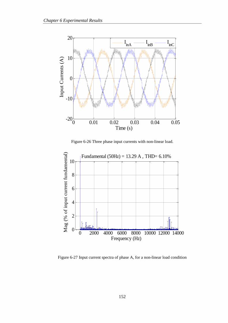
Chapter 6 Experimental Results
152
Figure 6-26 Three phase input currents with non-linear load.
Figure 6-27 Input current spectra of phase A, for a non-linear load condition
0 0.01 0.02 0.03 0.04 0.05-20
-10
0
10
20
Time (s)
Inp
ut
Cu
rren
ts (
A)
IinA
IinB
IinC
0 2000 4000 6000 8000 10000 12000 140000
2
4
6
8
10
Frequency (Hz)
Fundamental (50Hz) = 13.29 A , THD= 6.10%
Mag
(%
of
inp
ut
curr
ent
fun
dam
enta
l)

Chapter 6 Experimental Results
153
6.6 Load connection and disconnection
Power converters, regardless of their application, may be used under very light or no
load condition and the controller must be able to maintain proper operation under
these conditions. In this section the experimental results for the four-leg Matrix
Converter is shown during load connection and disconnection.
Figure 6-28 and Figure 6.29 shows the experimental results for the four-leg Matrix
Converter during load disconnection and connection. The load is disconnected and
reconnected to test the performance of the converter for a step change in the output
current. As can be seen from these results, the controller was able to provide good
waveform quality with only a less than 28% output voltage overshoot / undershoot
for each transient.
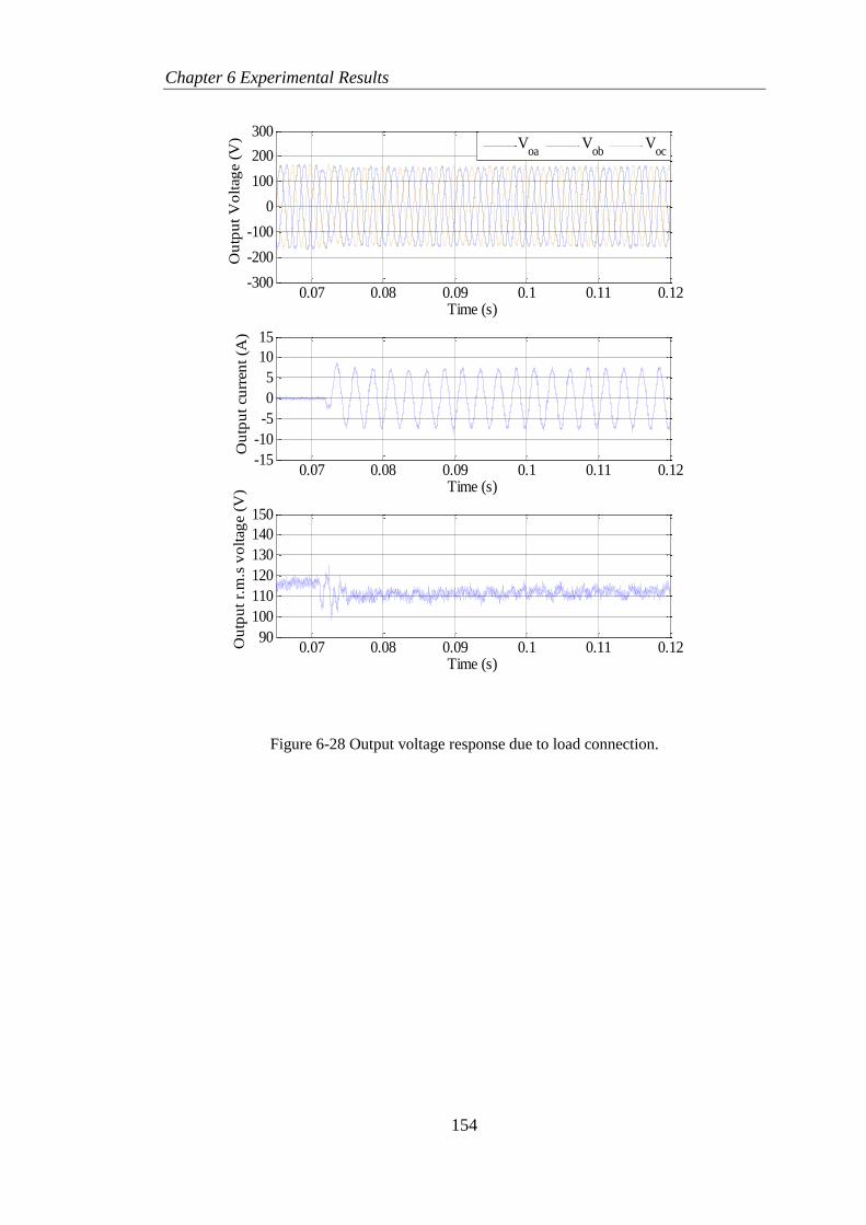
Chapter 6 Experimental Results
154
Figure 6-28 Output voltage response due to load connection.
0.07 0.08 0.09 0.1 0.11 0.12-300
-200
-100
0
100
200
300
Time (s)
Ou
tpu
t V
olt
age
(V)
V
oaV
obV
oc
0.07 0.08 0.09 0.1 0.11 0.12-15
-10
-5
0
5
10
15
Time (s)
Ou
tpu
t cu
rren
t (A
)
0.07 0.08 0.09 0.1 0.11 0.1290
100
110
120
130
140
150
Time (s)
Ou
tpu
t r.
m.s
vo
ltag
e (V
)
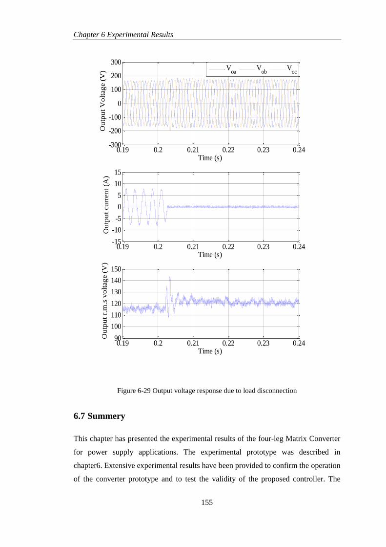
Chapter 6 Experimental Results
155
Figure 6-29 Output voltage response due to load disconnection
6.7 Summery
This chapter has presented the experimental results of the four-leg Matrix Converter
for power supply applications. The experimental prototype was described in
chapter6. Extensive experimental results have been provided to confirm the operation
of the converter prototype and to test the validity of the proposed controller. The
0.19 0.2 0.21 0.22 0.23 0.24-300
-200
-100
0
100
200
300
Time (s)
Ou
tpu
t V
olt
age
(V)
V
oaV
obV
oc
0.19 0.2 0.21 0.22 0.23 0.24-15
-10
-5
0
5
10
15
Time (s)
Ou
tpu
t cu
rren
t (A
)
0.19 0.2 0.21 0.22 0.23 0.2490
100
110
120
130
140
150
Time (s)
Ou
tpu
t r.
m.s
vo
ltag
e (V
)
Chapter 6 Experimental Results
156
repetitive controller discussed in chapter 3 has been used to test the converter
prototype during different load conditions. It can be seen that the experimental
results showed in this chapter matches the simulation results provided in chapter 4.
The use of the repetitive and second order controller in ABC reference frame has the
privilege to control the output voltage of the four-leg Matrix Converter individually.
In the first part of this chapter, experimental results of the four-leg Matrix Converter
supplying balanced load has been presented and it can be seen that the output voltage
is tracking the reference with a tracking error less than ± 8V in both simulation and
experimental results. Next, the experimental results of the converter prototype
supplying an unbalanced load are presented to demonstrate the ability of the
proposed controller to regulate the output voltage. It can be seen that the tracking
error between the reference and the output voltage is less than ± 10V for the
simulation results while it is ± 20V for the experimental results. Then, the
experimental results of the converter prototype connected to a non-linear load are
showed. It can be clearly seen that the controller able is able to control the 5th
and the
7th
harmonics and again a good match between the simulation and the experimental
results was obtained.
Finally, to test the stability of the proposed controller to a sudden change in the
output current from zero to full load, by connecting and disconnecting the load
completely. As can be seen from these results, the controller was able to provide
good waveform quality with only 28% output voltage overshoot / undershoot for
each transient.The performance of the Matrix Converter system employing repetitive
and tracking controller in ABC reference frame is presented in Table 6-2.
As can be seen in Table 6-2, there are some considerable differences between the
simulation and experimental results. Thses differences are due to many factors that
we do not consider during the simulations such as the voltage drop across the
switches, commutation delay, non-linear magnetic component, for example.
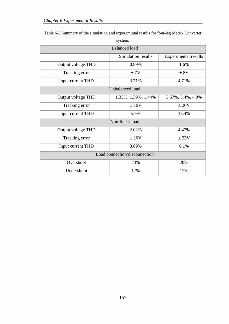
Chapter 6 Experimental Results
157
Table 6-2 Summary of the simulation and experemintal results for four-leg Matrix Converter
system.
Balanced load
Simulation results Experimental results
Output voltage THD 0.89% 1.6%
Tracking error ± 7V ± 8V
Input current THD 3.71% 4.71%
Unbalanced load
Output voltage THD 1.33%, 1.39%, 1.44% 3.67%, 5.4%, 4.8%
Tracking error ± 10V ± 20V
Input current THD 5.9% 13.4%
Non-linear load
Output voltage THD 2.02% 4.47%
Tracking error ± 10V ± 23V
Input current THD 3.89% 6.1%
Load connection/disconnection
Overshoot 23% 28%
Undershoot 17% 17%

Chapter 7: Conclusion
158
Chapter 7 Conclusion
7.1 Conclusion
This thesis has investigated the suitability of four-leg matrix converter for
400Hz ground power unit applications. For aircraft ground power unit applications,
where different loads needs to be supplied, ranging from single phase to three phase
balanced and unbalanced and also non-linear loads, 3x3 matrix converters will not
deliver high performance because the converter needs to be able to deal with zero
sequence current in the system. Therefore, four-leg Matrix Converters, featuring a
neutral connection, is used to produce a balanced output voltage even under
unbalanced or non-linear load conditions.
Ground power units (GPU) are designed to provide a high quality power supply to
the aircraft at airports with 400Hz, 115V. A 400 Hz system is used in application
where space and weight are important factors. Due to the high fundamental
frequency, passive components in 400Hz frequency are much smaller; this means
Chapter 7: Conclusion
159
that the system will be lighter and the take less volume. For regulation of a converter
output voltage with a 400Hz output frequency, a high bandwidth controller is
required. However, the controller bandwidth is limited due to the reduced ratio
between the converter switching frequency and the fundamental frequency. To avoid
this problem a digital repetitive controller is proposed in a single voltage loop
configuration operating in the ABC reference frame.
Repetitive control (RC) provides a possible control solution for systems, like this
one, presenting a repetitive behaviour, to minimize or eliminate periodic waveform
errors and to improve output power quality. The use of an internal current loop is not
attractive in this application due to bandwidth limitations. If an internal current loop
was included, it should be much faster than the external voltage loop, which needs to
be very fast itself, to be able to meet the very strict transient specifications on the
output voltage required for this application. Therefore the implementation of a faster
internal current loop becomes impractical with the use of standard control platforms
and with the limitations on the converter switching frequency.
A repetitive control is therefore used in conjunction with a conventional linear
controller to regulate the output voltage during different load conditions, such as
balanced and un-balanced linear loads, non-linear loads and during load connection
and disconnection.
The first objective of this work was to develop a four-leg Matrix Converter model to
be used in the control design and simulation work. This model is required to test the
performance of the proposed controller under steady state and transients. The details
of converter model and modulation methods were discussed in chapter 2. In this
chapter, a relationship between Venturini and Space vector modulation for four-leg
Matrix Converter has been developed and it becomes easy to convert the duty cycles
to time and vectors.
The second objective was to develop a control strategy to regulate the output voltage
of the converter, presented in chapter 3; the controller consists of a second order
linear controller combined with a plug-in type repetitive controller. The second order
linear controller serves to improve system dynamics in transient conditions, while the
Chapter 7: Conclusion
160
repetitive controller serves to eliminate any periodic error and improve the steady
state response of the system. This is achieved using a single voltage control loop
implemented in the ABC reference frame.
The third aim of the work was to simulate the four-leg Matrix Converter and the
proposed controller to evaluate the performance of the plug-in repetitive controller
during different load conditions presented in chapter 4. In this context MATLAB/
Simulink package is used to design the controller while SABER simulation package
have been used to simulate the whole system during steady state and transients.
The fourth objective was to develop, build and test a reduced scale experimental rig
to validate the simulation results, presented in chapter 5. The system consists of input
filter, output filter, bidirectional switches, gate drive unit, and the control platform.
The control algorithm was programmed in the DSP/FPGA control platform that has
been developed in the PEMC research group at the University of Nottingham. In
addition, experimental results were presented in chapter 6. The converter prototype
has been shown to operate successfully and excellent agreement between simulation
results and practical data has been shown. In chapter 6 experimental results of the
four-leg Matrix Converter supplying balanced load has been presented and it can be
seen that the output voltage tracks the reference with an error less than ± 8V. Next,
the experimental results of the converter prototype supplying an unbalanced load are
presented to demonstrate the ability of the proposed controller to regulate the output
voltage. It can be seen that the tracking error between the reference and the output
voltage is less than ± 10V. Then, experimental results when the converter prototype
is connected to a non-linear load are shown. It can be clearly seen that the controller
able is able to control the 5th
and the 7th
harmonics and again a good match between
the simulation and experimental results was obtained.
Finally, the stability and performance of the proposed system to a sudden change in
the output current from zero to full load has been tested by connecting and
disconnecting the load completely. As it can be seen from these results, the controller
was able to provide good waveform quality with only 28% output voltage overshoot /
undershoot for each transient. The results showed that the use of the repetitive and

Chapter 7: Conclusion
161
second order controller in ABC reference frame has the advantage to control the
output voltage of the four-leg Matrix Converter individually.
7.2 Future work
The following are some interesting topics in which further research can be carried
out in order to improve the four-leg Matrix Converter for 400Hz power supply
applications.
Efficiency analysis. In this work the converter losses have not been evaluated
nor compared with traditional configurations. This is definitely one of the
most important next steps of this research.
Use of high switching frequency. If high switching frequency is used higher
control bandwidth can be obtained; input and output filter size will be smaller
and high power density can be achieved. This may be possible by using
power modules with fast switching frequency, low losses and high power
such as SiC JFETs.
EMI (Electro Magnetic Interference). EMI has also not been analysed in this
thesis. Proper measurement and input/output EMI filter design will be needed
in order to pursue an industrialization of this solution.
References
162
References
[1] P. Zanchetta, J. C. Clare, P. Wheeler, D. Katsis, M. Bland, and L.
Empringham, "Control Design of a Three-phase Matrix Converter Mobile AC
Power Supply using Genetic Algorithms," 2005, pp. 2370-2375.
[2] Patrick Wheeler, "AC/AC Converters," in Power Electronics and Motor
Drives, Bogdan M. Wilmowski; J. David Irwin, Ed., 2 ed New York, USA:
CRC Press, 2011.
[3] U. B. Jensen, F. Blaabjerg, and J. K. Pedersen, "A new control method for
400-Hz ground power units for airplanes," IEEE Transactions on Industry
Applications, vol. 36, pp. 180-187, 2000.
[4] S. L. Arevalo, P. Zanchetta, and P. W. Wheeler, "Control of a Matrix
Converter-based AC Power Supply for Aircrafts under Unbalanced
Conditions," in Industrial Electronics Society, 2007. IECON 2007. 33rd
Annual Conference of the IEEE, 2007, pp. 1823-1828.
[5] D. o. d. i. standard., "Military standard-aircraft electric power characteristics,"
ed: Department of defense interface standard. , 2004.
[6] B. A. Francis, and Wonham, W. M., "The Internal Model Principle of Control
Theory ." Automatica. 457–465, vol. 12 (5), pp. 457–465, 1976.
[7] Y. Wang, F. Gao, and F. J. Doyle Iii, "Survey on iterative learning control,
repetitive control, and run-to-run control," Journal of Process Control, vol.
19, pp. 1589-1600, 2009.
[8] A. Alesina and M. Venturini, "Solid-state power conversion: A Fourier
analysis approach to generalized transformer synthesis," IEEE Transactions
on Circuits and Systems, vol. 28, pp. 319-330, 1981.
[9] A. Alesina and M. G. B. Venturini, "Analysis and design of optimum-
amplitude nine-switch direct AC-ACconverters," IEEE Transactions on
Power Electronics, vol. 4, pp. 101-112, 1989.
[10] J. Rodriguez, "A new control technique for AC-AC converters," in IFAC
Control in Power Electronics and Electrical Drives 1983, pp. 203–208.
[11] M. Braun and K. Hasse, "A direct frequency changer with control of input
reactive power," IFAC Control in Power Electronics and Electrical Drives,
pp. 187-194, 1983.
[12] G. Kastner and J. Rodriguez, "A forced commutated cycloconverter with
control of the source and load currents," in EPE’85, 1985, pp. 1141–1146.
References
163
[13] D. Casadei, G. Serra, A. Tani, and L. Zarri, "Matrix converter modulation
strategies: a new general approach based on space-vector representation of
the switch state," Industrial Electronics, IEEE Transactions on, vol. 49, pp.
370-381, 2002.
[14] Nicholas J. Mason, "Space Vector Modulation of a 4-Leg Matrix Converter,"
PhD, Electrical and Electronic engineering, University of Nottingham, 2011.
[15] N. Burany, "Safe control of four-quadrant switches," in Industry Applications
Society Annual Meeting, 1989., Conference Record of the 1989 IEEE, 1989,
pp. 1190-1194 vol.1.
[16] L. Empringham, P. W. Wheeler, and J. C. Clare, "Intelligent commutation of
matrix converter bi-directional switch cells using novel gate drive
techniques," in Power Electronics Specialists Conference, 1998. PESC 98
Record. 29th Annual IEEE, 1998, pp. 707-713 vol.1.
[17] L. Huber, D. Borojevic, and N. Burany, "Voltage space vector based PWM
control of forced commutated cycloconverters," in Industrial Electronics
Society, 1989. IECON '89., 15th Annual Conference of IEEE, 1989, pp. 106-
111 vol.1.
[18] J. Mahlein, J. Igney, J. Weigold, M. Braun, and O. Simon, "Matrix converter
commutation strategies with and without explicit input voltage sign
measurement," Industrial Electronics, IEEE Transactions on, vol. 49, pp.
407-414, 2002.
[19] P. W. Wheeler, J. C. Clare, L. Empringharn, M. Bland, and M. Apap, "Gate
drive level intelligence and current sensing for matrix converter current
commutation," Industrial Electronics, IEEE Transactions on, vol. 49, pp.
382-389, 2002.
[20] P. Nielsen, F. Blaabjerg, and J. K. Pedersen, "Novel solutions for protection
of matrix converter to three phase induction machine," in Industry
Applications Conference, 1997. Thirty-Second IAS Annual Meeting, IAS '97.,
Conference Record of the 1997 IEEE, 1997, pp. 1447-1454 vol.2.
[21] J. Mahlein, M. Bruckmann, and M. Braun, "Passive protection strategy for a
drive system with a matrix converter and an induction machine," Industrial
Electronics, IEEE Transactions on, vol. 49, pp. 297-303, 2002.
[22] C. Klumpner, P. Nielsen, I. Boldea, and F. Blaabjerg, "New solutions for a
low-cost power electronic building block for matrix converters," Industrial
Electronics, IEEE Transactions on, vol. 49, pp. 336-344, 2002.
[23] F. Blaabjerg, D. Casadei, C. Klumpner, and M. Matteini, "Comparison of two
current modulation strategies for matrix converters under unbalanced input
voltage conditions," Industrial Electronics, IEEE Transactions on, vol. 49,
pp. 289-296, 2002.
References
164
[24] J. M. Lozano and J. M. Ramirez, "Matrix converter performance under
unbalanced input-voltage," in Power Symposium, 2008. NAPS '08. 40th North
American, 2008, pp. 1-6.
[25] K. B. Lee, C. H. Bae, and F. Blaabjerg, "An improved DTC-SVM method for
matrix converter drives using a deadbeat scheme," International Journal of
Electronics, vol. 93, pp. 737-753, 2006.
[26] K. Lee and F. Blaabjerg, "Improved direct torque control for sensorless
matrix converter drives with constant switching frequency and torque ripple
reduction," INTERNATIONAL JOURNAL OF CONTROL AUTOMATION
AND SYSTEMS, vol. 4, p. 113, 2006.
[27] F. Jurado, M. Ortega, and A. Cano, "Predictive Control of Matrix Converter-
based Micro-turbine," Electric Power Components and Systems, vol. 36, pp.
409 - 431, 2008.
[28] S. Pinto and J. Silva, "Sliding mode direct control of matrix converters,"
Electric Power Applications, IET, vol. 1, pp. 439-448, 2007.
[29] T. Inoue, M. Nakano, T. Kubo, S. Matsumoto, and H. Baba, "High accuracy
control of a proton synchrotron magnet power supply," 1982, p. 3137.
[30] C. Rech and J. R. Pinheiro, "New repetitive control system of PWM inverters
with improved dynamic performance under non-periodic disturbances," in
IEEE Power Electronics Specialists Conference, 2004, pp. 54-60.
[31] J. Shuai, C. Dong, and F. Z. Peng, "High performance repetitive control for
three-phase CVCF PWM inverter using a 4th-order linear phase IIR filter," in
Applied Power Electronics Conference and Exposition (APEC), 2012
Twenty-Seventh Annual IEEE, 2012, pp. 225-231.
[32] K. Zhang, Y. Kang, J. Xiong, and J. Chen, "Direct repetitive control of
SPWM inverter for UPS purpose," IEEE Transactions on Power Electronics,
vol. 18, pp. 784-792, 2003.
[33] C. Rech, H. Pinheiro, H. A. Grundling, H. L. Hey, and J. R. Pinheiro,
"Analysis and design of a repetitive predictive-PID controller for PWM
inverters," 2001, pp. 986-994.
[34] Z. Keliang, W. Danwei, and X. Guangyan, "Repetitive controlled three-phase
reversible PWM rectifier," in American Control Conference, 2000.
Proceedings of the 2000, 2000, pp. 125-129 vol.1.
[35] K. Zhou and D. Wang, "Digital repetitive controlled three-phase PWM
rectifier," IEEE Transactions on Power Electronics, vol. 18, pp. 309-316,
2003.
[36] W. Chengzhi, Z. Yunping, Z. Yun, X. Yun, S. Xu, and L. Fen, "Research on
the single-phase PWM rectifier based on the repetitive control," in Industrial
References
165
Technology, 2008. ICIT 2008. IEEE International Conference on, 2008, pp.
1-6.
[37] W. M. Rohouma, S. L. Arevalo, P. Zanchetta, and P. Wheeler, "Repetitive
control for a four leg matrix converter," in Power Electronics, Machines and
Drives (PEMD 2010), 5th IET International Conference., 2010, pp. 1-6.
[38] W. M. Rohouma, L. de Lillo, S. Lopez, P. Zanchetta, and P. W. Wheeler, "A
single loop repetitive voltage controller for a four legs matrix converter
ground power unit," in Power Electronics and Applications (EPE 2011),
Proceedings of the 2011-14th European Conference on, 2011, pp. 1-9.
[39] C. Cosner, G. Anwar, and M. Tomizuka, "Plug in repetitive control for
industrial robotic manipulators," in Robotics and Automation, 1990.
Proceedings., 1990 IEEE International Conference on, 1990, pp. 1970-1975
vol.3.
[40] J. H. Moon, M. N. Lee, and M. J. Chung, "Repetitive control for the track-
following servo system of an optical disk drive," IEEE transactions on
control systems technology, vol. 6, pp. 663-670, 1998.
[41] K. K. Chew and M. Tomizuka, "Digital control of repetitive errors in disk
drive systems," Control Systems Magazine, IEEE, vol. 10, pp. 16-20, 1990.
[42] D. Tae-Yong and R. Jung Rae, "Robust repetitive controller design and its
application on the track-following control system in optical disk drives," in
Decision and Control and European Control Conference (CDC-ECC), 2011
50th IEEE Conference on, 2011, pp. 1644-1649.
[43] S. Ferreira Pinto and J. Fernando Silva, "Input filter design for sliding mode
controlled matrix converters," in Power Electronics Specialists Conference,
2001. PESC. 2001 IEEE 32nd Annual, 2001, pp. 648-653 vol.2.
[44] D. Casadei, J. Clare, E. Lee, G. Serra, A. Tani, A. Trentin, P. Wheeler, and L.
Zarri, "Large-Signal Model for the Stability Analysis of Matrix Converters,"
Industrial Electronics, IEEE Transactions on, vol. 54, pp. 939-950, 2007.
[45] S. Pinto and J. Silva, "Input Filter Design of a Mains Connected Matrix
Converter," in Session on Power Electronics Mitigation Methods for Power
Quality, IEEE-Power Engineering Society International Conference on
Harmonics and Quality of Power, Cascais, Portugal, 2006.
[46] R. W. Erickson, "Optimal single resistors damping of input filters," in
Applied Power Electronics Conference and Exposition, 1999. APEC '99.
Fourteenth Annual, 1999, pp. 1073-1079 vol.2.
[47] P. W. Wheeler, P. Zanchetta, J. C. Clare, L. Empringham, M. Bland, and D.
Katsis, "A utility power supply based on a four-output leg matrix converter,"
IEEE Transactions on Industry Applications, vol. 44, pp. 174-186, 2008.

References
166
[48] R. Cardenas, R. Pena, P. Wheeler, and J. Clare, "Experimental Validation of a
Space-Vector-Modulation Algorithm for Four-Leg Matrix Converters,"
Industrial Electronics, IEEE Transactions on, vol. 58, pp. 1282-1293, 2011.
[49] P. Potamianos, E. Mitronikas, and A. Safacas, "Open-Circuit Fault Diagnosis
for Matrix Converter Drives and Remedial Operation Using Carrier-Based
Modulation Methods," Industrial Electronics, IEEE Transactions on, vol. PP,
pp. 1-1, 2013.
[50] M. Rivera, J. Rodriguez, C. Garcia, R. Pena, and J. Espinoza, "A simple
predictive voltage control method with unity displacement power factor for
four-leg indirect matrix converters," in Power Electronics and Motion
Control Conference (EPE/PEMC), 2012 15th International, 2012, pp.
DS2c.5-1-DS2c.5-6.
[51] S. L. Arevalo, "Matrix Converter for Frequency Changing Power Supply
Applications," Ph.D, Electrical and Electronic engineering, University of
Nottingham, 2008.
[52] P. JenoPaul, T. Prakash, and I. J. Reglend, "Power quality improvement for
matrix converter using unified power quality conditioner," Transactions of
the Institute of Measurement and Control, 2011.
[53] C. Hanju and T. K. Vu, "Comparative analysis of low-pass output filter for
single-phase grid-connected Photovoltaic inverter," in Applied Power
Electronics Conference and Exposition (APEC), 2010 Twenty-Fifth Annual
IEEE, 2010, pp. 1659-1665.
[54] R. Zhang, "High performance power converter systems for nonlinear and
unbalanced load/source," PhD, Virginia Polytechnic Institute and State
University, 1998.
[55] P. W. Wheeler, J. Rodriguez, J. C. Clare, L. Empringham, and A. Weinstein,
"Matrix converters: a technology review," IEEE Transactions on Industrial
Electronics, vol. 49, pp. 276-288, 2002.
[56] S. Bernet, T. Matsuo, and T. A. Lipo, "A Matrix Converter Using Reverse
Blocking NPT-IGBT's and Optimized Pulse Patterns," 1996, pp. 107-113.
[57] L. de Lillo, " A Matrix Converter Drive System for an Aircraft Rudder
Electro-Mechanical Actuator, Ph.D. thesis," Electrical and Electronic
engineering, University of Nottingham, 2006.
[58] C. T. Pan, T. C. Chen, and J. J. Shieh, "A zero switching loss matrix
converter," in Power Electronics Specialists Conference, 1993. PESC '93
Record., 24th Annual IEEE, 1993, pp. 545-550.
[59] M. V. M. Villaca and A. J. Perin, "A soft switched direct frequency changer,"
in Industry Applications Conference, 1995. Thirtieth IAS Annual Meeting,
IAS '95., Conference Record of the 1995 IEEE, 1995, pp. 2321-2326 vol.3.
References
167
[60] C. J. G. a. C. G.H., " Soft Switched Matrix Converter for High Frequency
Direct AC-to-AC Power Conversion, Conf. Rec. EPE’91, Firenze, 1991, pp4-
196-4-201.," 1991,.
[61] M. Apap, J. C. Clare, P. W. Wheeler, and K. J. Bradley, "Analysis and
comparison of AC-AC matrix converter control strategies," in Power
Electronics Specialist Conference, 2003. PESC '03. 2003 IEEE 34th Annual,
2003, pp. 1287-1292 vol.3.
[62] J. Rodriguez, M. Rivera, J. W. Kolar, and P. W. Wheeler, "A Review of
Control and Modulation Methods for Matrix Converters," Industrial
Electronics, IEEE Transactions on, vol. 59, pp. 58-70, 2012.
[63] F. L. Luo, H. Ye, and M. H. Rashid, Digital power electronics and
applications: Academic Press, 2005.
[64] M. J. Ryan, R. W. De Doncker, and R. D. Lorenz, "Decoupled control of a
four-leg inverter via a new 4×4 transformation matrix," Power
Electronics, IEEE Transactions on, vol. 16, pp. 694-701, 2001.
[65] M. Venturini, "A new sine wave in, sine wave out, conversion technique
eliminates reactive elements," in Proc. Powercon 7, pp. E3-1-E3-15., 1980,
pp. E3-1-E3-15.
[66] A. Yazdani and R. Iravani, Voltage-Sourced converters in power systems:
Wiley Online Library, 2010.
[67] S. Lopez Arevalo, P. Zanchetta, P. W. Wheeler, A. Trentin, and L.
Empringham, "Control and implementation of a matrix converter based AC
ground power supply unit for aircraft servicing," Industrial Electronics, IEEE
Transactions on, vol. 57, pp. 2076-2084, 2010.
[68] Z. Li, P. Wang, H. Zhu, Y. Li, L. Tan, Y. Chen, and F. Gao, "A new digital
control method for high performance 400 Hz ground power unit," 2008, pp.
515-520.
[69] Z. Li, Y. Li, P. Wang, H. Zhu, C. Liu, and F. Gao, "Single-Loop Digital
Control of High-Power 400-Hz Ground Power Unit for Airplanes," Industrial
Electronics, IEEE Transactions on, vol. 57, pp. 532-543, 2009.
[70] Z. Haibin, L. Yaohua, L. Zixin, and W. Ping, "Design and Performance
Analysis of High Power Static 400-Hz Supply," in Power and Energy
Engineering Conference, 2009. APPEEC 2009. Asia-Pacific, 2009, pp. 1-4.
[71] L. Mihalache, "DSP control of 400 Hz inverters for aircraft applications," in
in Industry Applications Conference, 2002. 37th IAS Annual Meeting., 2002,
pp. 1564-1571.
References
168
[72] P. Zanchetta, P. Wheeler, L. Empringham, and J. Clare, "Design control and
implementation of a three-phase utility power supply based on the matrix
converter," Power Electronics, IET, vol. Volume 2, pp. 156 - 162, 2009.
[73] T. C. Tsao and K. K. Chew, "Analysis and synthesis of discrete-time
repetitive controllers," Journal of Dynamic Systems, Measurement, and
Control, vol. 111, p. 353, 1989.
[74] H. Yingjie, L. Jinjun, W. Zhaoan, and Z. Yunping, "An Improved Repetitive
Control for Active Power Filters with Three-Level NPC Inverter," in Applied
Power Electronics Conference and Exposition, 2009. APEC 2009. Twenty-
Fourth Annual IEEE, 2009, pp. 1583-1588.
[75] X. H. Wu, S. K. Panda, and J. X. Xu, "Design of a Plug-In Repetitive Control
Scheme for Eliminating Supply-Side Current Harmonics of Three-Phase
PWM Boost Rectifiers Under Generalized Supply Voltage Conditions,"
Power Electronics, IEEE Transactions on, vol. 25, pp. 1800-1810, 2010.
[76] M. Jamil, " Repetitive current control of two-level and interleaved three-
phase PWM utility connected converters.," Faculty of Engineering and the
Environment,, University of Southampton, Doctoral Thesis., 2012.
[77] M. Tomizuka, T.-C. Tsao, and K.-K. Chew, "Discrete-Time Domain Analysis
and Synthesis of Repetitive Controllers," in American Control Conference,
1988, 1988, pp. 860-866.
[78] P. Mattavelli, L. Tubiana, and M. Zigliotto, "Torque-ripple reduction in PM
synchronous motor drives using repetitive current control," Power
Electronics, IEEE Transactions on, vol. 20, pp. 1423-1431, 2005.
[79] Z. Keliang and D. Wang, "Digital repetitive controlled three-phase PWM
rectifier," Power Electronics, IEEE Transactions on, vol. 18, pp. 309-316,
2003.
[80] G. F. Franklin, J. D. Powell, and A. Emami-Naeini, Feedback control of
dynamic systems vol. 3: Addison-Wesley Reading, MA, 1994.
[81] Y. Y. Tzou, R. S. Ou, S. L. Jung, and M. Y. Chang, "High-performance
programmable AC power source with low harmonic distortion using DSP-
based repetitive control technique," Power Electronics, IEEE Transactions
on, vol. 12, pp. 715 - 725 July 1997.
[82] M. Guizani, A. Rayes, B. Khan, and A. Al-Fuqaha, Network Modeling and
Simulation: A Practical Perspective: Wiley-Interscience, 2010.
[83] T. Wu, S. V. Bozhko, G. M. Asher, and D. W. P. Thomas, "Accelerated
functional modeling of aircraft electrical power systems including fault
scenarios," in Industrial Electronics, 2009. IECON '09. 35th Annual
Conference of IEEE, 2009, pp. 2537-2544.
References
169
[84] T. Wu, S. V. Bozhko, G. M. Asher, and D. W. Thomas, "Fast functional
modelling of the aircraft power system including line fault scenarios," in
Power Electronics, Machines and Drives (PEMD 2010), 5th IET
International Conference on, 2010, pp. 1-7.
[85] R. Caroline, "Investigation into the stability of matrix converter systems,"
PhD, Electrical and electronics engineering department, University of
Nottingham, 2008.
[86] D. Casadei, G. Serra, A. Tani, and L. Zarri, "Effects of input voltage
measurement on stability of matrix converter drive system," Electric Power
Applications, IEE Proceedings -, vol. 151, pp. 487-497, 2004.
[87] B. s. a. series, "General requirements for ground support electrical supplies
for aircraft," ed: Aerospace Standards Committee, 1983.
[88] B. W. Augdahl, H. L. Hess, B. K. Johnson, and D. C. Katsis, "Output
protection strategies for battlefield power supplied by matrix converters," in
Power Symposium, 2005. Proceedings of the 37th Annual North American,
2005, pp. 151-158.
[89] J. C. Clare, L. Empringham, and P. W. Wheeler, "The effects of sampling
delays and nonideal filtering on the performance of matrix converter
modulation algorithms," in Power Electronics and Variable Speed Drives,
2000. Eighth International Conference on (IEE Conf. Publ. No. 475), 2000,
pp. 29-34.
[90] J. Andreu, I. Kortabarria, E. Ormaetxea, E. Ibarra, J. L. Martin, and S.
Apinaniz, "A Step Forward Towards the Development of Reliable Matrix
Converters," Industrial Electronics, IEEE Transactions on, vol. 59, pp. 167-
183, 2012.
[91] M. P. Kazmierkowski, R. Krishnan, and F. Blaabjerg, Control in power
electronics: selected problems: Academic Pr, 2002.
[92] Semikron. (19.12.2010). Available:
http://www.semikron.com/products/data/cur/assets/SK_60_GM_123_USA_2
4509004.pdf
[93] F. Yue, "Invistigation of modulation techniques for matrix converters, Ph.D.
thesis," Ph.D, Electrical and Electronic engineering, University of
Nottingham, 2007.
[94] LEM. (2010, 19-12-2010). LEM-current tranducer, voltage transducer,
sensor, power measurment. Available:
http://www.lem.com/hq/en/content/view/176/126/
[95] J. Kim, J. Choi, and H. Hong, "Output LC filter design of voltage source
inverter considering the performance of controller," in Power System

References
170
Technology, 2000. Proceedings. PowerCon 2000. International Conference
on, 2000, pp. 1659-1664 vol.3.
[96] Texas Instruments. (01/08/2012). Code Composer Studio (CCStudio)
Integrated Development Environment (IDE). Available:
http://www.ti.com/tool/ccstudio
[97] Chroma, "Programmable AC Source 61705," User's Manual, 2007.," 2007.
Appendices
171
Appendices
Appendix A : Published Papers
The work has resulted in the following papers having been published:
[1] W. M. Rohouma, S. L. Arevalo, P. Zanchetta, and P. Wheeler, "Repetitive
control for a four-leg Matrix Converter," in Power Electronics, Machines and Drives
(PEMD 2010), 5th IET International Conference., 2010, pp. 1-6.
[2] W. M. Rohouma, L. de Lillo, S. Lopez, P. Zanchetta, and P. W. Wheeler, "A
single loop repetitive voltage controller for a four-legs Matrix Converter ground
power unit," in Power Electronics and Applications (EPE 2011), Proceedings of the
2011-14th European Conference on, 2011, pp. 1-9.
[3] W. M. Rohouma, L. Empringham, P. Zanchetta, and P. W. Wheeler, "A four-
legs Matrix Converter based ground power unit with selective harmonic control," in
Energy Conversion Congress and Exposition (ECCE), 2011 IEEE, Phoenix, Arizona,
USA, 2011, pp. 799-805.
Under revision journal paper:
Wesam M. Rohouma, Pericle Zanchetta, Patrick W Wheeler, Lee Empringham, A
Four-Legs Matrix Converter Ground Power Unit with Repetitive Voltage Control
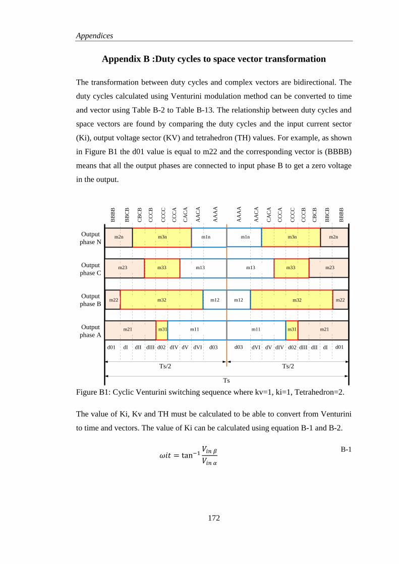
Appendices
172
Appendix B :Duty cycles to space vector transformation
The transformation between duty cycles and complex vectors are bidirectional. The
duty cycles calculated using Venturini modulation method can be converted to time
and vector using Table B-2 to Table B-13. The relationship between duty cycles and
space vectors are found by comparing the duty cycles and the input current sector
(Ki), output voltage sector (KV) and tetrahedron (TH) values. For example, as shown
in Figure B1 the d01 value is equal to m22 and the corresponding vector is (BBBB)
means that all the output phases are connected to input phase B to get a zero voltage
in the output.
Ts
d01 dI dII dIII d02 dIV dV dVI d03 d03 dVI dV dIV d02 dIII dII dI d01
m2n m3n m1n m1n m3n m2n
m23 m33 m13 m13 m33 m23
m22 m32 m12 m12 m32 m22
m21 m31 m11 m11 m31 m21
Ts/2 Ts/2
BB
BB
BB
CB
CB
CB
CC
CB
CC
CC
CC
CA
CA
CA
AA
CA
AA
AA
Output
phase N
Output
phase C
Output
phase B
Output
phase A
AA
AA
AA
CA
CA
CA
CC
CA
CC
CC
CC
CB
CB
CB
BB
CB
BB
BB
Figure B1: Cyclic Venturini switching sequence where kv=1, ki=1, Tetrahedron=2.
The value of Ki, Kv and TH must be calculated to be able to convert from Venturini
to time and vectors. The value of Ki can be calculated using equation B-1 and B-2.
B-1
Appendices
173
where Ki <7 and >=1
B-2
Similarly The value of Kv can be found from equation B-3, and B-4.
B-3
where Kv< 7 and >=1
B-4
Finally, the value of tetrahedron can be found by comparing the sign of the three
phases demand voltages, as shown in Table B-1.
Table B-1: Tetrahedron selection according to the demand voltage polarity and prism
number.
Tetrahedron
1
V*AN V*BN V*CN
2
V*AN V*BN V*CN
3
V*AN V*BN V*CN
4
V*AN V*BNV*CN
Pri
sms
1 + + + + + - - + - - - -
2 + + + + + - - + - - - -
3 + + + - + + - + - - - -
4 + + + - + + - - + - - -
5 + + + + - + - - + - - -
6 + + + + - + + - - - - -

Appendices
174
Table B-2: Ki = 1 , Tetrahedron = 2
Table B-3: Ki = 1 , Tetrahedron = 3
Kv = 1 Kv = 2 Kv = 3 Kv = 4 Kv = 5 Kv = 6
d01 t31 t32 t32 t33 t33 t31
d02 t13 t13 t11 t11 t12 t12
d03 t21 t22 t22 t23 t23 t21
dI t32 – t31 t31 – t32 t33 – t32 t32 – t33 t31 – t33 t33 - 31
dII t3n – t32 t3n – t31 t3n – t33 t3n – t32 t3n – t31 t3n – t33
dIII t33 – t3n t33 – t3n t31 – t3n t31 – t3n t32 –t3n t32 – t3n
dIV t23 – t2n t23 – t2n t21 – t2n t21 – t2n t22 – t2n t22 – t2n
dV t2n – t22 t2n – t21 t2n – t23 t2n – t22 t2n – t21 t2n – t23
dVI t22 – t21 t21 – t22 t23 – t22 t22 – t23 t21 - 23 t23 – t21
Kv = 1 Kv = 2 Kv = 3 Kv = 4 Kv = 5 Kv = 6
d01 t31 t32 t32 t33 t33 t31
d02 t13 t13 t11 t11 t12 t12
d03 t21 t22 t22 t23 t23 t21
dI t3n – t31 t3n – t32 t3n – t32 t3n – t33 t3n – t33 t3n – t31
dII t32 – t3n t31 – t3n t33 – t3n t32 – t3n t31 – t3n t33 – t3n
dIII t33 – t32 t33 – t31 t31 – t33 t31 – t32 t32 – t31 t32 – t33
dIV t23 – t22 t23 – t21 t21 – t23 t21 – t22 t22 – t21 t22 – t23
dV t22 – t2n t21 – t2n t23 – t2n t22 – t2n t21 – t2n t23 – t2n
dVI t2n – t21 t2n – t22 t2n – t22 t2n –t23 t2n –t23 t2n – t21

Appendices
175
Table B-4: Ki = 2 , Tetrahedron = 2
Table B-5: Ki = 2 , Tetrahedron = 3
Kv = 1 Kv = 2 Kv = 3 Kv = 4 Kv = 5 Kv = 6
d01 t23 t23 t21 t21 t22 t22
d02 t31 t32 t32 t33 t33 t31
d03 t13 t13 t11 t11 t12 t12
dI t2n – t23 t2n – t23 t2n – t21 t2n – t21 t2n – t22 t2n – t22
dII t22 – t2n t21 – t2n t23 – t2n t22 – t2n t21 – t2n t23 – t2n
dIII t21 – t22 t22 – t21 t22 – t23 t23 – t22 t23 – t21 t21 – t23
dIV t11- t12 t12 – t11 t12 – t13 t13 – t12 t13 – t11 t11 – t13
dV t12 – t1n t11 – t1n t13 – t1n t12 – t1n t11 – t1n t13 – t1n
dVI t1n t13 t1n – t13 t1n – t11 t1n – t11 t1n – t12 t1n – t12
Kv = 1 Kv = 2 Kv = 3 Kv = 4 Kv = 5 Kv = 6
d01 t23 t23 t21 t21 t22 t22
d02 t31 t32 t32 t33 t33 t31
d03 t13 t13 t11 t11 t12 t12
dI t22 – t23 t21 – t23 t23 – t21 t22 – t21 t21 – t22 t23 – t22
dII t2n – t22 t2n – t21 t2n – t23 t2n – t22 t2n – t21 t2n – t23
dIII t21 – t2n t22 – t2n t22 – t2n t23 – t2n t23 – t2n t21 – t2n
dIV t11 – t1n t12 – t1n t12 – t1n t13 – t1n t13 – t1n t11 – t1n
dV t1n – t12 t1n – t11 t1n – t13 t1n – t12 t1n – t11 t1n – t13
dVI t12 – t13 t11 – t13 t13 – t11 t12 – t11 t11 – t12 t13 – t12

Appendices
176
Table B-6: Ki = 3 , Tetrahedron = 2
Table B-7: Ki = 3 , Tetrahedron = 3
Kv = 1 Kv = 2 Kv = 3 Kv = 4 Kv = 5 Kv = 6
d01 t11 t12 t12 t13 t13 t11
d02 t23 t23 t21 t21 t22 t22
d03 t31 t32 t32 t33 t33 t31
Di t12 – t11 t11 – t12 t13 – t12 t12 – t13 t11 – t13 t13 – t11
dII t1n – t12 t1n – t11 t1n – t13 t1n – t12 t1n – t11 t1n – t13
dIII t13 – t1n t13 – t1n t11 – t1n t11 – t1n t12 – t1n t12 – t1n
dIV t33 – t3n t33 – t3n t31 – t3n t31 – t3n t32 – t3n t32 – t3n
dV t3n – t32 t3n – t31 t3n – t33 t3n – t32 t3n – t31 t3n – t33
dVI t32 – t31 t31 – t32 t33 – t32 t32 – t33 t31 – t33 t33 – t31
Kv = 1 Kv = 2 Kv = 3 Kv = 4 Kv = 5 Kv = 6
d01 t11 t12 t12 t13 t13 t11
d02 t23 t23 t21 t21 t22 t22
d03 t31 t32 t32 t33 t33 t31
dI t1n – t11 t1n – t12 t1n – t12 t1n – t13 t1n – t13 t1n – t11
dII t12 – t1n t11 – t1n t13 – t1n t12 – t1n t11 – t1n t13 – t1n
dIII t13 – t12 t13 – t11 t11 – t13 t11 – t12 t12 – t11 t12 – t13
dIV t33 – t32 t33 – t31 t31 – t33 t31 – t32 t32 – t31 t32 – t33
dV t32 – t3n t31 – t3n t33 – t3n t32 – t3n t31 – t3n t33 – t3n
dVI t3n – t31 t3n – t32 t3n – t32 t3n – t33 t3n – t33 t3n – t31

Appendices
177
Table B-8: Ki = 4 , Tetrahedron = 2
Table B-9: Ki = 4 , Tetrahedron = 3
Kv = 1 Kv = 2 Kv = 3 Kv = 4 Kv = 5 Kv = 6
d01 t33 t33 t31 t31 t32 t32
d02 t11 t12 t12 t13 t13 t11
d03 t23 t23 t21 t21 t22 t22
dI t3n – t33 t3n – t33 t3n – t31 t3n – t31 t3n – t32 t3n – t32
dII t32 – t3n t31 – t3n t33 – t3n t32 – t3n t31 – t3n t33 – t3n
dIII t31 – t32 t32 – t31 t32 – t33 t33 – t32 t33 – t31 t31 – t33
dIV t21 – t22 t22 – t21 t22 – t23 t23 – t22 t23 – t21 t21 – t23
dV t22 – t2n t21 – t2n t23 – t2n t22 – t2n t21 – t2n t23 – t2n
dVI t2n –t23 t2n –t23 t2n – t21 t2n – t21 t2n – t22 t2n – t22
Kv = 1 Kv = 2 Kv = 3 Kv = 4 Kv = 5 Kv = 6
d01 t33 t33 t31 t31 t32 t32
d02 t11 t12 t12 t13 t13 t11
d03 t23 t23 t21 t21 t22 t22
dI t32 – t33 t31 – t33 t33 - 31 t32 – t31 t31 – t32 t33 – t32
dII t3n – t32 t3n – t31 t3n – t33 t3n – t32 t3n – t31 t3n – t33
dIII t31 – t3n t32 –t3n t32 – t3n t33 – t3n t33 – t3n t31 – t3n
dIV t21 – t2n t22 – t2n t22 – t2n t23 – t2n t23 – t2n t21 – t2n
dV t2n – t22 t2n – t21 t2n – t23 t2n – t22 t2n – t21 t2n – t23
dVI t22 – t23 t21 - 23 t23 – t21 t22 – t21 t21 – t22 t23 – t22

Appendices
178
Table B-10: Ki = 5 , Tetrahedron = 2
Table B-11: Ki = 5 , Tetrahedron = 3
Kv = 1 Kv = 2 Kv = 3 Kv = 4 Kv = 5 Kv = 6
d01 t21 t22 t22 t23 t23 t21
d02 t33 t33 t31 t31 t32 t32
d03 t11 t12 t12 t13 t13 t11
dI t22 – t21 t21 – t22 t23 – t22 t22 – t23 t21 – t23 t23 – t21
dII t2n – t22 t2n – t21 t2n – t23 t2n – t22 t2n – t21 t2n – t23
dIII t23 – t2n t23 – t2n t21 – t2n t21 – t2n t22 – t2n t22 – t2n
dIV t13 – t1n t13 – t1n t11 – t1n t11 – t1n t12 – t1n t12 – t1n
dV t1n – t12 t1n – t11 t1n – t13 t1n – t12 t1n – t11 t1n – t13
dVI t12 – t11 t11 – t12 t13 – t12 t12 – t13 t11 – t13 t13 – t11
Kv = 1 Kv = 2 Kv = 3 Kv = 4 Kv = 5 Kv = 6
d01 t21 t22 t22 t23 t23 t21
d02 t33 t33 t31 t31 t32 t32
d03 t11 t12 t12 t13 t13 t11
dI t2n – t21 t2n – t22 t2n – t22 t2n – t23 t2n – t23 t2n – t21
dII t22 – t2n t21 – t2n t23 – t2n t22 – t2n t21 – t2n t23 – t2n
dIII t23 – t22 t23 – t21 t21 – t23 t21 – t22 t22 – t21 t22 – t23
dIV t13 – t12 t13 – t11 t11 – t13 t11- t12 t12 – t11 t12 – t13
dV t12 – t1n t11 – t1n t13 – t1n t12 – t1n t11 – t1n t13 – t1n
dVI t1n – t11 t1n – t12 t1n – t12 t1n t13 t1n – t13 t1n – t11
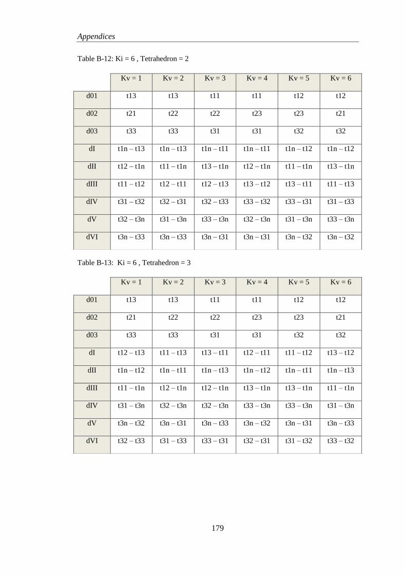
Appendices
179
Table B-12: Ki = 6 , Tetrahedron = 2
Table B-13: Ki = 6 , Tetrahedron = 3
Kv = 1 Kv = 2 Kv = 3 Kv = 4 Kv = 5 Kv = 6
d01 t13 t13 t11 t11 t12 t12
d02 t21 t22 t22 t23 t23 t21
d03 t33 t33 t31 t31 t32 t32
dI t1n – t13 t1n – t13 t1n – t11 t1n – t11 t1n – t12 t1n – t12
dII t12 – t1n t11 – t1n t13 – t1n t12 – t1n t11 – t1n t13 – t1n
dIII t11 – t12 t12 – t11 t12 – t13 t13 – t12 t13 – t11 t11 – t13
dIV t31 – t32 t32 – t31 t32 – t33 t33 – t32 t33 – t31 t31 – t33
dV t32 – t3n t31 – t3n t33 – t3n t32 – t3n t31 – t3n t33 – t3n
dVI t3n – t33 t3n – t33 t3n – t31 t3n – t31 t3n – t32 t3n – t32
Kv = 1 Kv = 2 Kv = 3 Kv = 4 Kv = 5 Kv = 6
d01 t13 t13 t11 t11 t12 t12
d02 t21 t22 t22 t23 t23 t21
d03 t33 t33 t31 t31 t32 t32
dI t12 – t13 t11 – t13 t13 – t11 t12 – t11 t11 – t12 t13 – t12
dII t1n – t12 t1n – t11 t1n – t13 t1n – t12 t1n – t11 t1n – t13
dIII t11 – t1n t12 – t1n t12 – t1n t13 – t1n t13 – t1n t11 – t1n
dIV t31 – t3n t32 – t3n t32 – t3n t33 – t3n t33 – t3n t31 – t3n
dV t3n – t32 t3n – t31 t3n – t33 t3n – t32 t3n – t31 t3n – t33
dVI t32 – t33 t31 – t33 t33 – t31 t32 – t31 t31 – t32 t33 – t32