Embed Size (px)
Citation preview
Design For ManufacturePresented by
Bill FrankMultek Applications Engineer
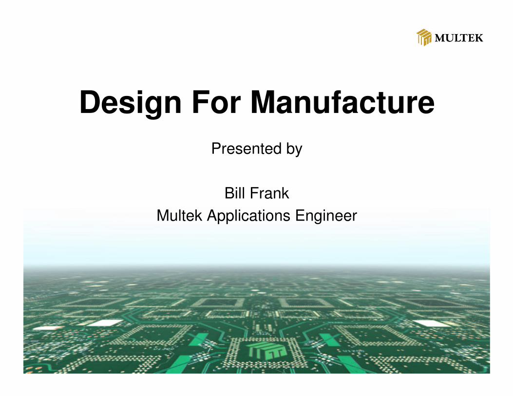
Discussion Agenda
•Goals and Objectives•DFM Process Flow •Board Layout – Analysis of Features•Board Layout – Yield Drivers •Electrical Test Issues•Stackups and Materials•HDI Design
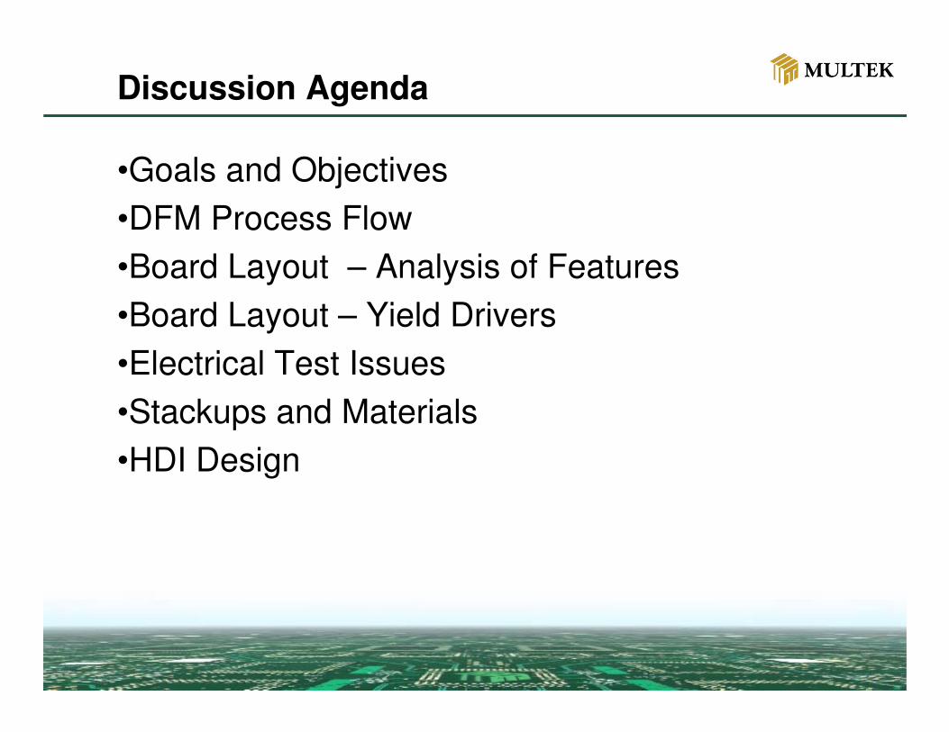
How?� Provide a “macro” review of the board design� Assist in meeting functional performance goals.� Help to eliminate surprises during factory tooling.� Assist with conveying development costs.� Maximize manufacturability of the design.� Help meet critical time to market goals.
Help Provide “Solutions”Design
Assembly DFA
PCB Fab DFF
DFxDFx
DFM Engineering Goals
DFM Process Flow
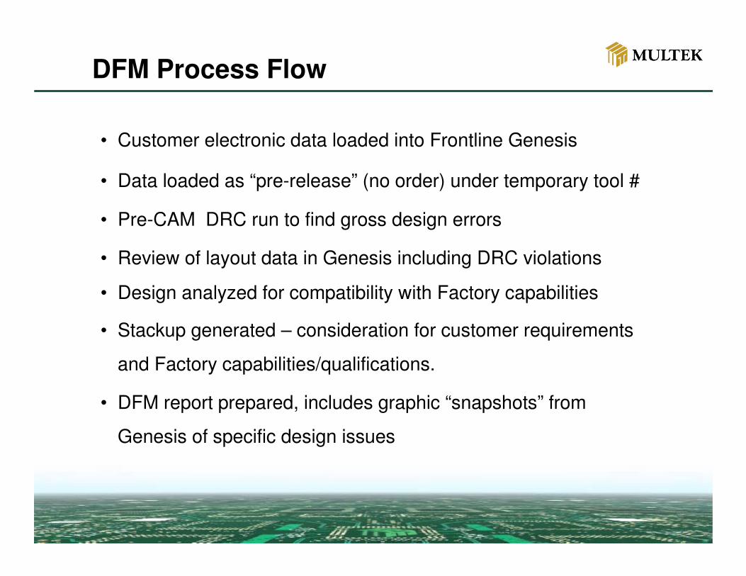
DFM Process Flow
• Customer electronic data loaded into Frontline Genesis
• Data loaded as “pre-release” (no order) under temporary tool #
• Pre-CAM DRC run to find gross design errors
• Review of layout data in Genesis including DRC violations
• Design analyzed for compatibility with Factory capabilities
• Stackup generated – consideration for customer requirements
and Factory capabilities/qualifications.
• DFM report prepared, includes graphic “snapshots” from
Genesis of specific design issues
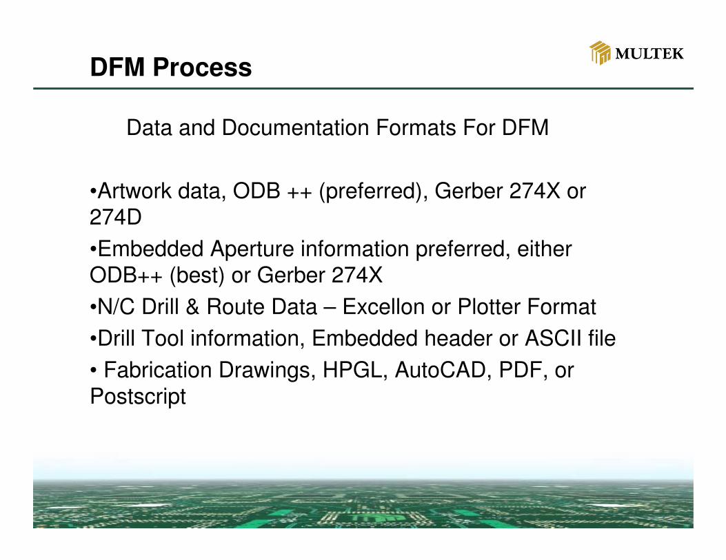
DFM Process
Data and Documentation Formats For DFM
•Artwork data, ODB ++ (preferred), Gerber 274X or 274D •Embedded Aperture information preferred, either ODB++ (best) or Gerber 274X •N/C Drill & Route Data – Excellon or Plotter Format •Drill Tool information, Embedded header or ASCII file • Fabrication Drawings, HPGL, AutoCAD, PDF, or Postscript
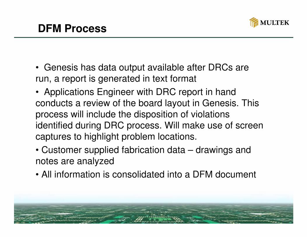
DFM Process
• Genesis has data output available after DRCs are run, a report is generated in text format • Applications Engineer with DRC report in hand conducts a review of the board layout in Genesis. This process will include the disposition of violations identified during DRC process. Will make use of screen captures to highlight problem locations. • Customer supplied fabrication data – drawings and notes are analyzed • All information is consolidated into a DFM document
DFM Process
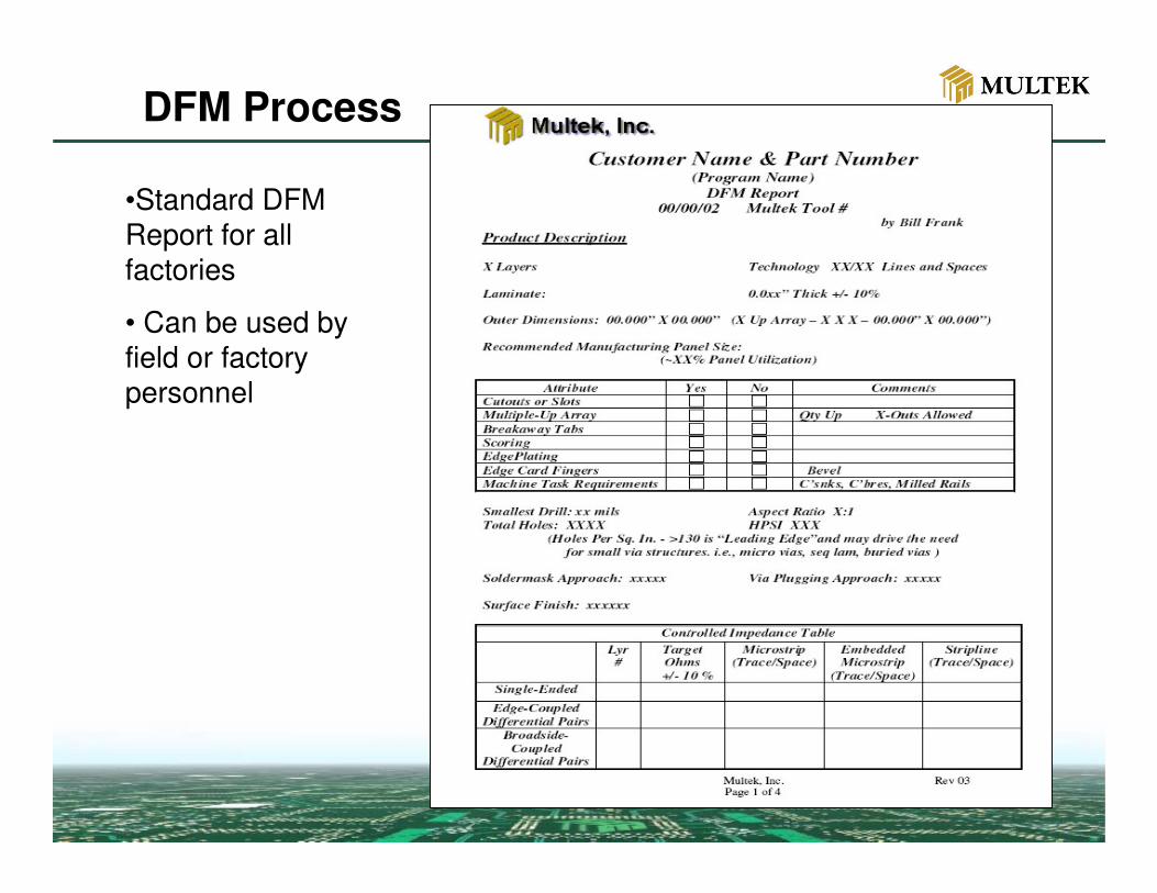
•Standard DFM Report for all factories
• Can be used by field or factory personnel

DFM Process
Section for recording of hole
sizes and features
Checklist of standard items
that effect factory yields
DFM Process
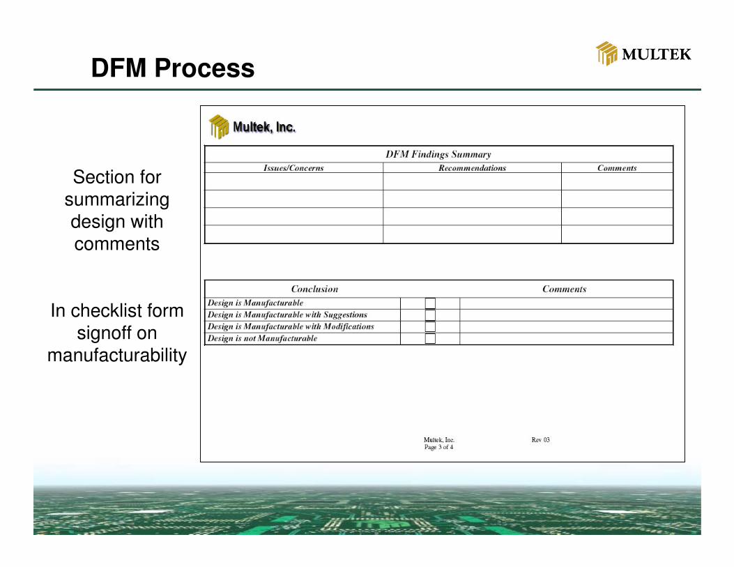
Section for summarizing design with comments
In checklist form signoff on
manufacturability
DFM Process
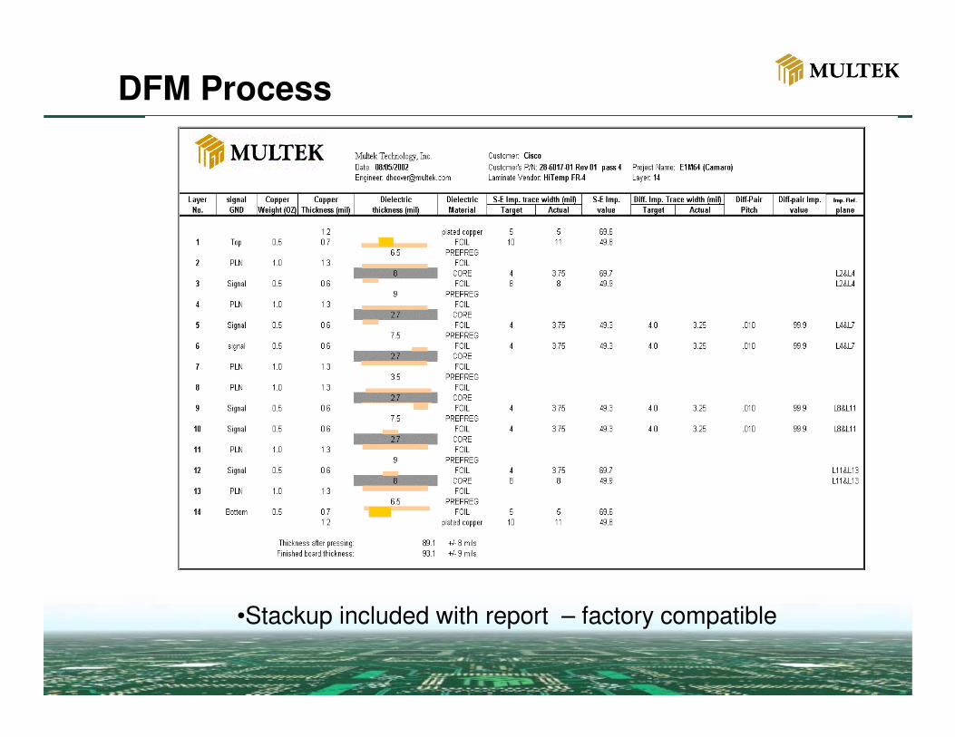
•Stackup included with report – factory compatible
Board Layout Guidelines
Board Layout – Analysis and Yield Drivers
• Analysis of board layout, review of lines, spaces, hole sizes, and related features is the heart of DFM process.•Inclusion or omission of certain features can significantly affect manufacturing yields.• Substantial amount of time is spent during the DFM analysis to identify and communicate potential layout issues• Slides in this section highlight feature types analyzed and typical yield drivers. Excerpted from the Multek Global PCB Fabrication Guide
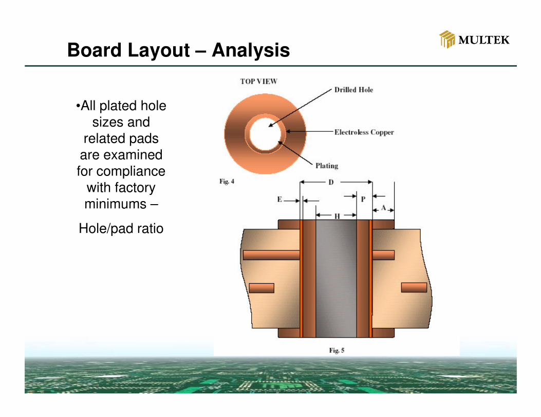
Board Layout – Analysis
•All plated hole sizes and
related pads are examined for compliance
with factory minimums –
Hole/pad ratio
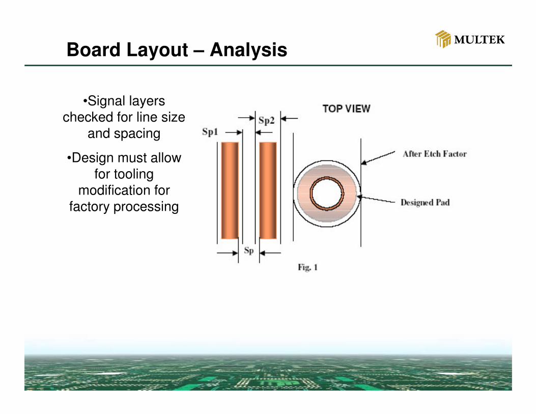
Board Layout – Analysis
•Signal layers checked for line size
and spacing
•Design must allow for tooling
modification for factory processing
Board Layout – Analysis
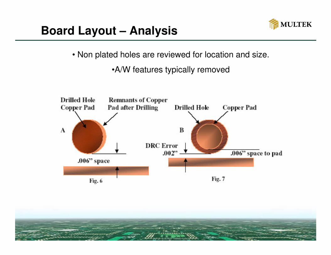
• Non plated holes are reviewed for location and size.
•A/W features typically removed
Board Layout – Analysis
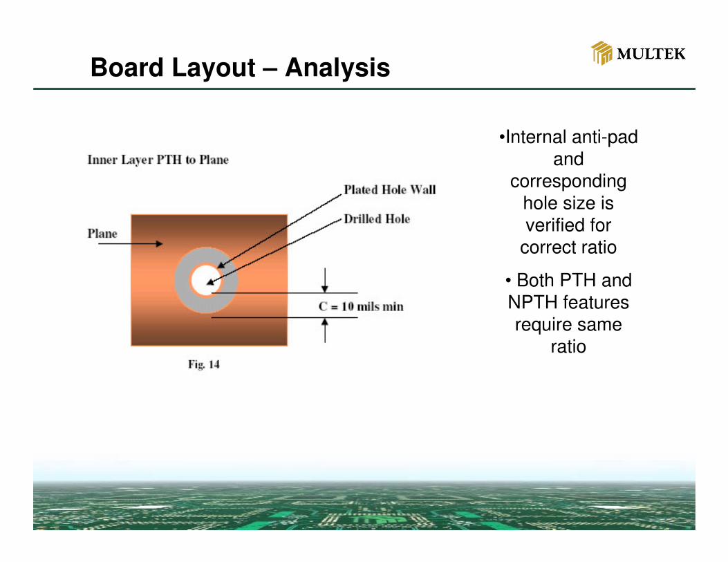
•Internal anti-pad and
corresponding hole size is verified for
correct ratio
• Both PTH and NPTH features require same
ratio
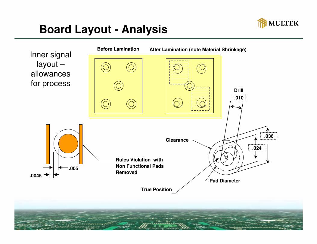
Board Layout - Analysis
Before Lamination After Lamination (note Material Shrinkage)
Clearance
True Position
.0045
Rules Violation withNon Functional PadsRemoved
Pad Diameter
.005
.024
.036
.010Drill
Inner signal layout –
allowances for process
Board Layout – Analysis
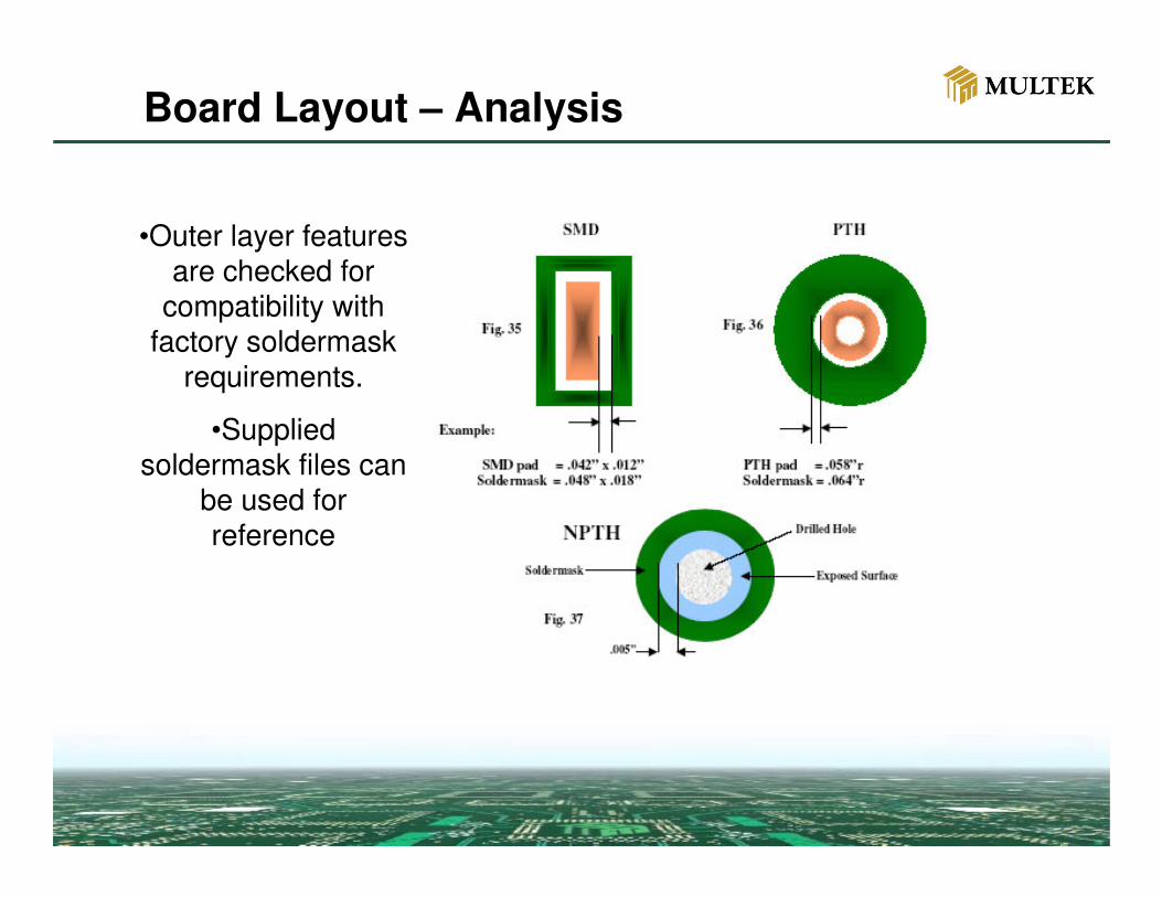
•Outer layer features are checked for
compatibility with factory soldermask
requirements.
•Supplied soldermask files can
be used for reference
Board Layout – Analysis
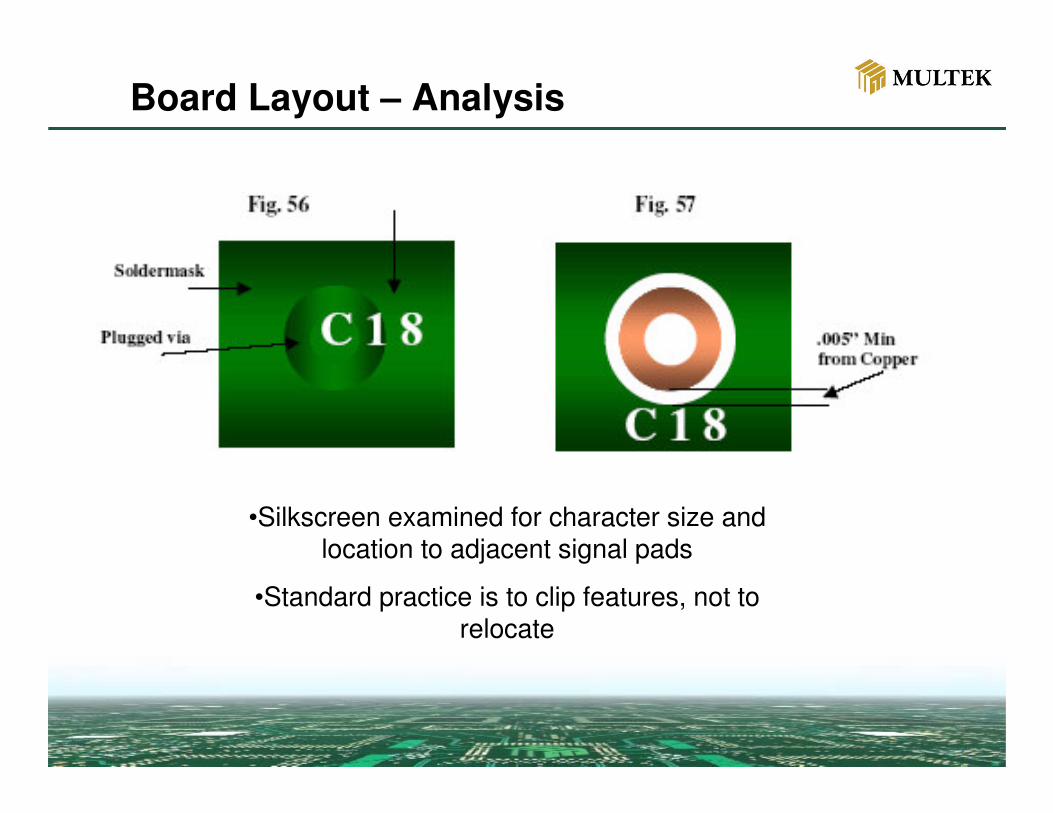
•Silkscreen examined for character size and location to adjacent signal pads
•Standard practice is to clip features, not to relocate
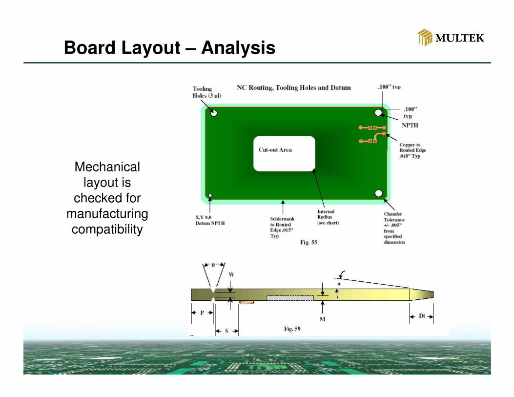
Board Layout – Analysis
Mechanical layout is
checked for manufacturing compatibility
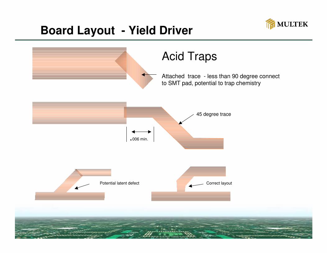
Board Layout - Yield Driver
Acid Traps
Attached trace - less than 90 degree connect to SMT pad, potential to trap chemistry
.006 min.
Potential latent defect Correct layout
45 degree trace
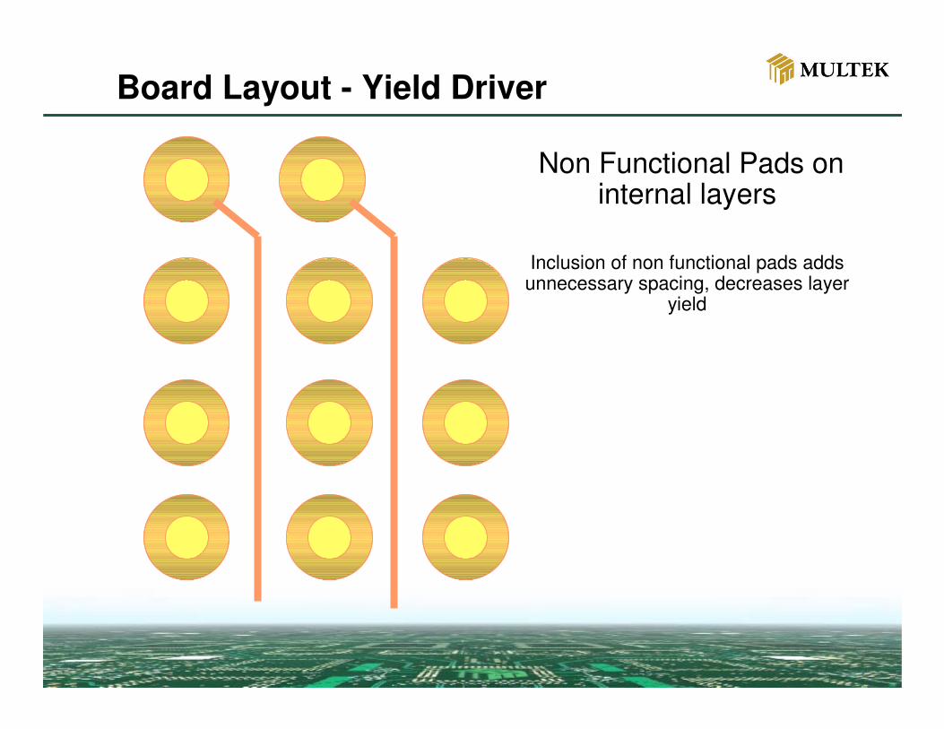
Board Layout - Yield Driver
Non Functional Pads on internal layers
Inclusion of non functional pads adds unnecessary spacing, decreases layer
yield
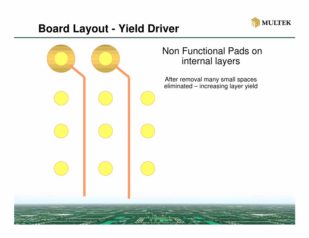
Board Layout - Yield Driver
Non Functional Pads on internal layers
After removal many small spaces eliminated – increasing layer yield
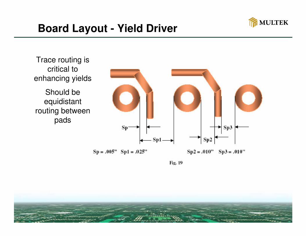
Board Layout - Yield Driver
Trace routing is critical to
enhancing yields
Should be equidistant
routing between pads
Board Layout - Yield Driver
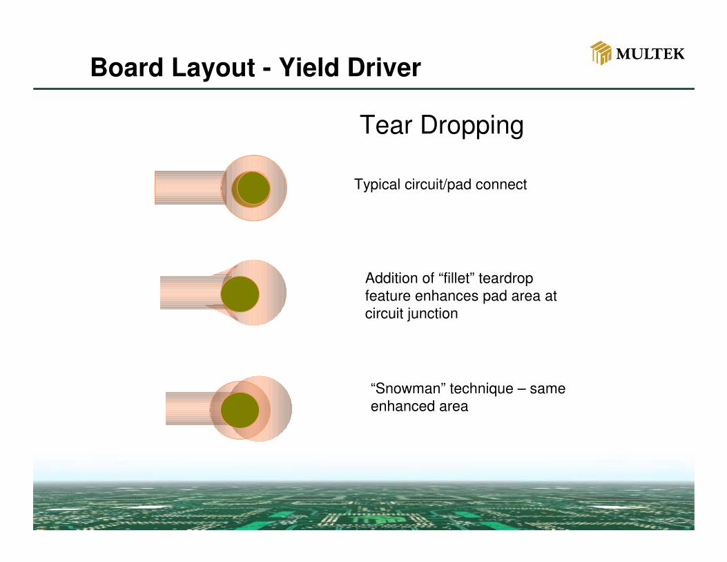
Tear Dropping
Typical circuit/pad connect
Addition of “fillet” teardrop feature enhances pad area at circuit junction
“Snowman” technique – same enhanced area
Board Layout - Yield Driver
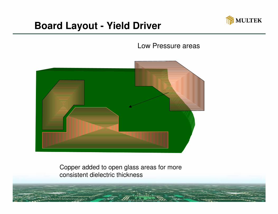
Low Pressure areas
Copper added to open glass areas for more consistent dielectric thickness
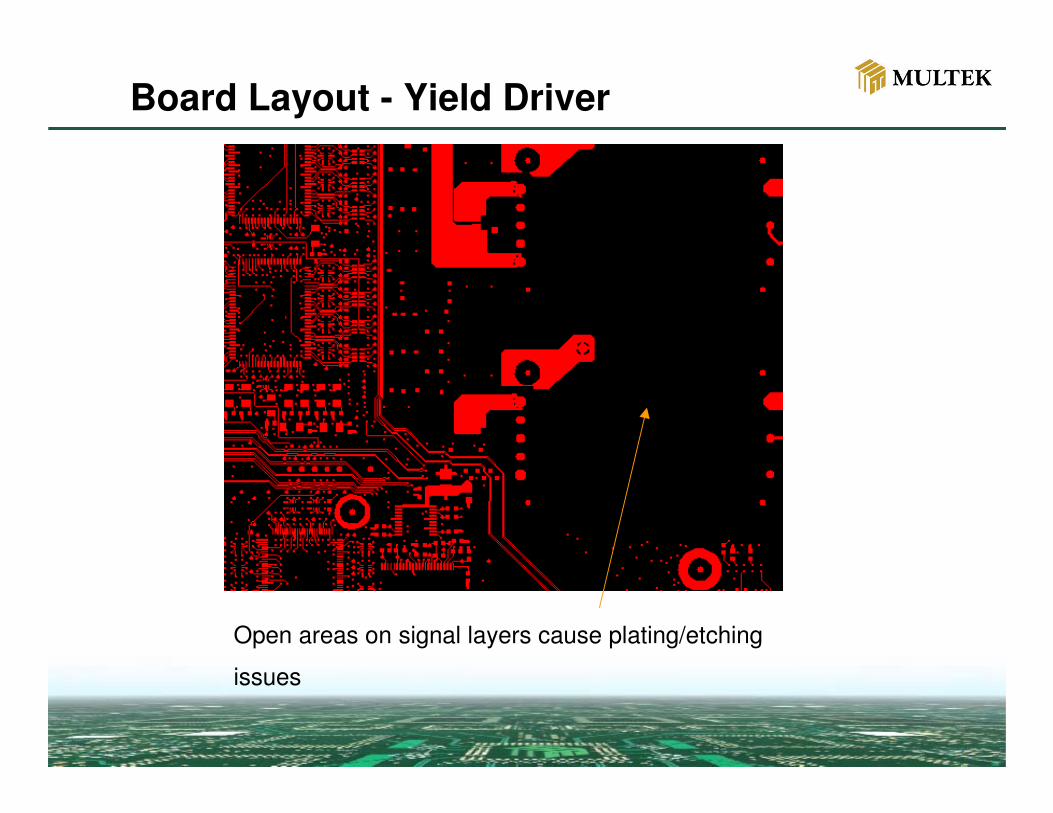
Board Layout - Yield Driver
Open areas on signal layers cause plating/etching
issues
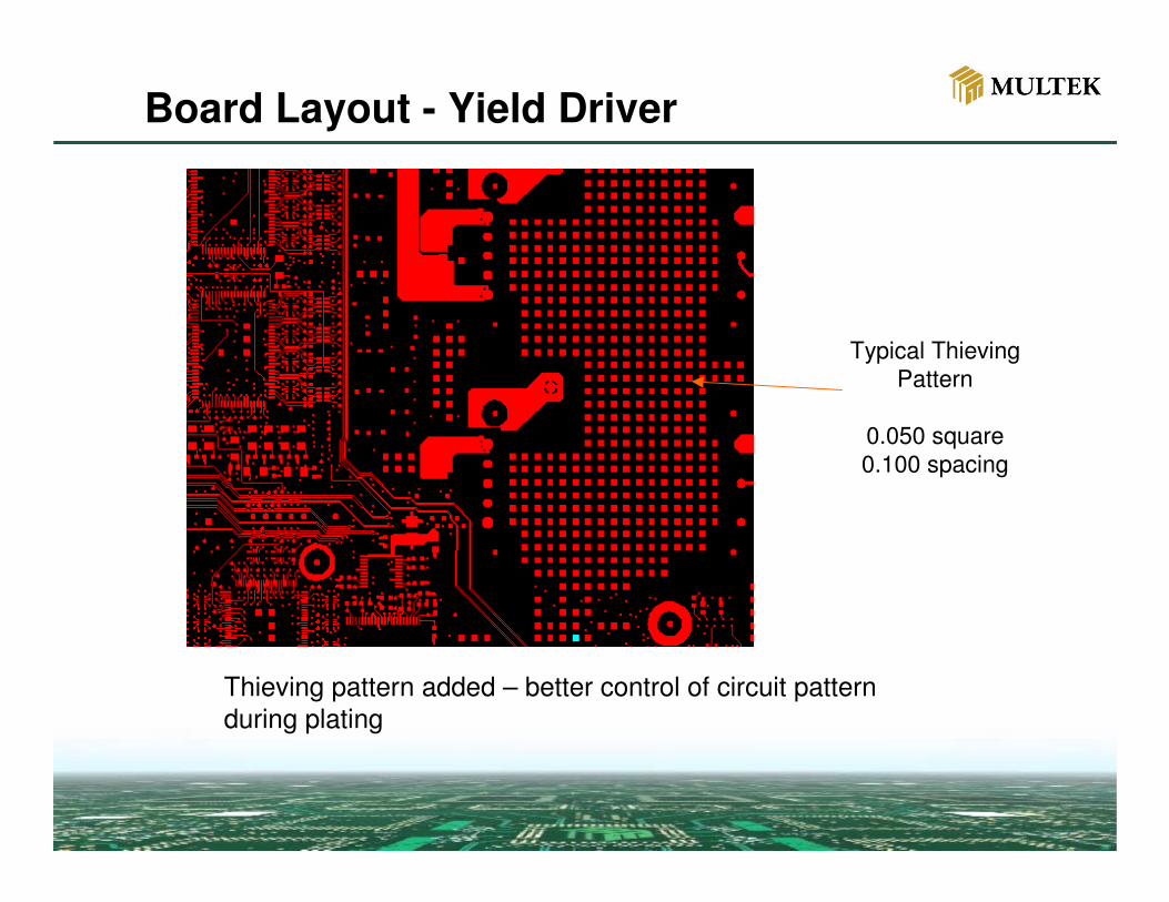
Board Layout - Yield Driver
Typical Thieving Pattern
0.050 square0.100 spacing
Thieving pattern added – better control of circuit pattern during plating
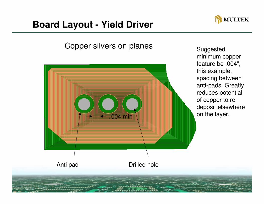
Board Layout - Yield Driver
Copper silvers on planes
.004 min
Suggested minimum copper feature be .004”, this example, spacing between anti-pads. Greatly reduces potential of copper to re-deposit elsewhere on the layer.
Anti pad Drilled hole
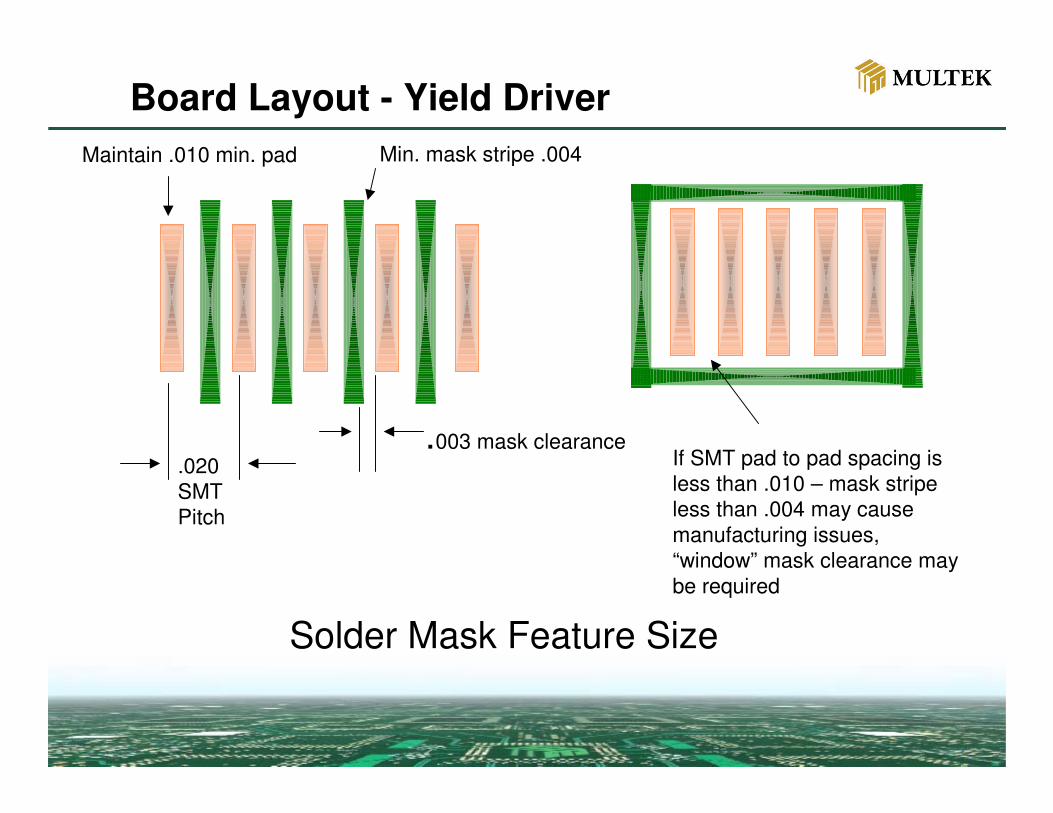
Board Layout - Yield Driver
Solder Mask Feature Size
.020 SMT Pitch
Maintain .010 min. pad
.003 mask clearance
Min. mask stripe .004
If SMT pad to pad spacing is less than .010 – mask stripe less than .004 may cause manufacturing issues, “window” mask clearance may be required

PCB Electrical Test
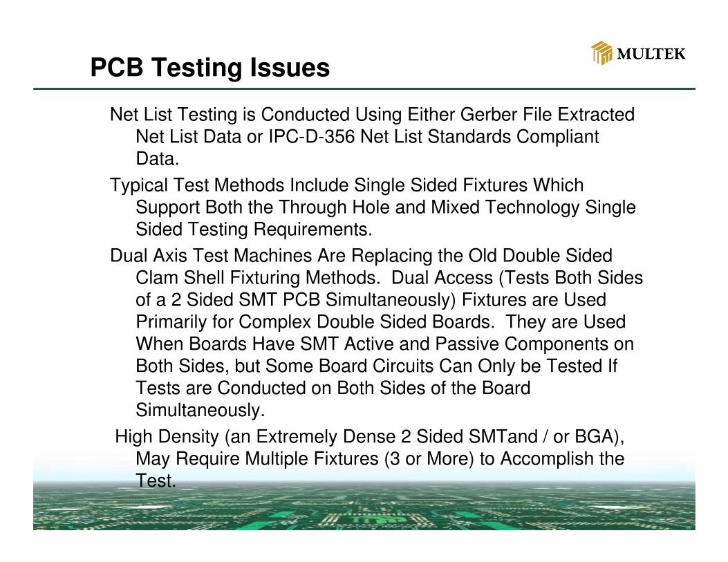
PCB Testing Issues
•Need to consider SMT Component pitch to determine board “testability”. May be necessary to contact the fabrication house for assistance. •Typically production level boards will use a fixtured method.•Boards with components at less than 16 mil pitch will require a “fixtureless” or flying probe test method. •Flying Probe test well suited for QTA/prototype work.•Test points should be a separate, distinct feature size. This allows maximum flexibility during tooling. •Good idea to standardize on the test point convention, use the same pad size, soldermask configuration, and side of the board where points are located.
PCB Testing Issues
Net List Testing is Conducted Using Either Gerber File ExtractedNet List Data or IPC-D-356 Net List Standards Compliant Data.
Typical Test Methods Include Single Sided Fixtures Which Support Both the Through Hole and Mixed Technology Single Sided Testing Requirements.
Dual Axis Test Machines Are Replacing the Old Double Sided Clam Shell Fixturing Methods. Dual Access (Tests Both Sides of a 2 Sided SMT PCB Simultaneously) Fixtures are Used Primarily for Complex Double Sided Boards. They are Used When Boards Have SMT Active and Passive Components on Both Sides, but Some Board Circuits Can Only be Tested If Tests are Conducted on Both Sides of the Board Simultaneously.
High Density (an Extremely Dense 2 Sided SMTand / or BGA), May Require Multiple Fixtures (3 or More) to Accomplish the Test.
Stackups and Materials
Stackups and Materials
• Stackup details – dielectric thickness and copper weights are reviewed for compatibility.• Is the dielectric thickness sufficient to fill the copper and give the specified final thickness?• Does the minimum hole size (drill) and final board thickness meet aspect ratio minimums?• Design should consider Z-axis expansion and ability of factory to plate adequate thickness of copper on the hole wall.•Does stackup meet electrical requirements?
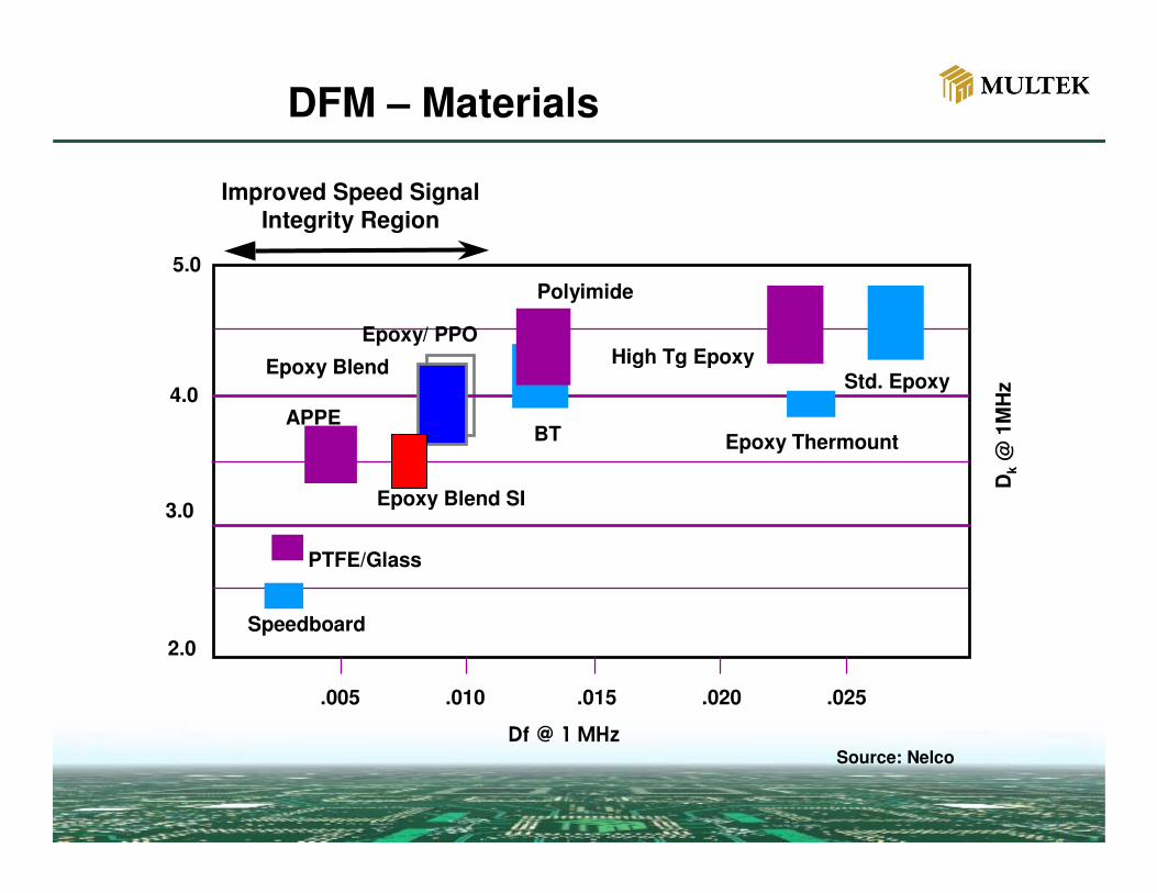
DFM – Materials
Dk
@ 1
MH
z4.0
3.0
2.0
.005 .010 .015 .020 .025
5.0
BT
Polyimide
Epoxy Blend
PTFE/Glass
Speedboard
High Tg Epoxy
Epoxy Thermount
Improved Speed Signal Integrity Region
Std. Epoxy
APPE
Df @ 1 MHz
Epoxy Blend SI
Epoxy/ PPO
Source: Nelco
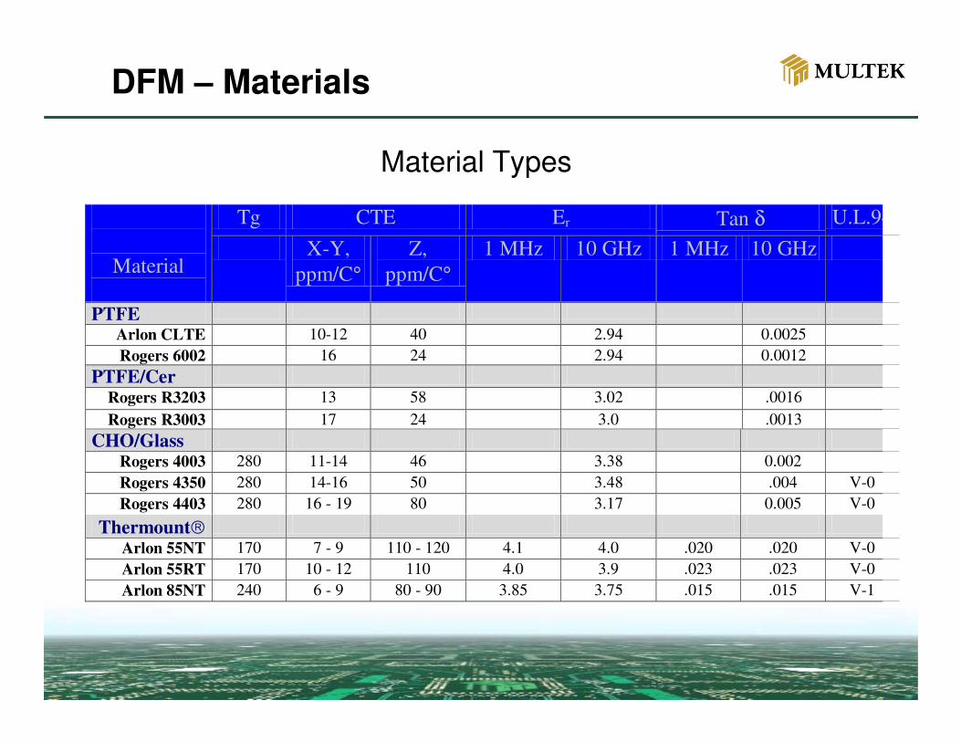
Tg CTE Er Tan δ U.L.94
Material
X-Y, ppm/C°
Z, ppm/C°
1 MHz 10 GHz 1 MHz 10 GHz
PTFE
Arlon CLTE 10-12 40 2.94 0.0025 Rogers 6002 16 24 2.94 0.0012
PTFE/Cer Rogers R3203 13 58 3.02 .0016 Rogers R3003 17 24 3.0 .0013
CHO/Glass Rogers 4003 280 11-14 46 3.38 0.002 Rogers 4350 280 14-16 50 3.48 .004 V-0 Rogers 4403 280 16 - 19 80 3.17 0.005 V-0
Thermount£ Arlon 55NT 170 7 - 9 110 - 120 4.1 4.0 .020 .020 V-0 Arlon 55RT 170 10 - 12 110 4.0 3.9 .023 .023 V-0 Arlon 85NT 240 6 - 9 80 - 90 3.85 3.75 .015 .015 V-1
DFM – Materials
Material Types
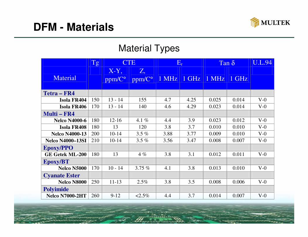
Tg CTE Er Tan δ U.L.94
Material
X-Y, ppm/C°
Z, ppm/C°
1 MHz
1 GHz
1 MHz
1 GHz
Tetra – FR4 Isola FR404 150 13 - 14 155 4.7 4.25 0.025 0.014 V-0 Isola FR406 170 13 - 14 140 4.6 4.29 0.023 0.014 V-0
Multi – FR4 Nelco N4000-6 180 12-16 4.1 % 4.4 3.9 0.023 0.012 V-0
Isola FR408 180 13 120 3.8 3.7 0.010 0.010 V-0 Nelco N4000-13 200 10-14 3.5 % 3.88 3.77 0.009 0.010 V-0
Nelco N4000–13SI 210 10-14 3.5 % 3.56 3.47 0.008 0.007 V-0 Epoxy/PPO GE Getek ML-200 180 13 4 % 3.8 3.1 0.012 0.011 V-0 Epoxy/BT
Nelco N5000 170 10 - 14 3.75 % 4.1 3.8 0.013 0.010 V-0 Cyanate Ester
Nelco N8000 250 11-13 2.5% 3.8 3.5 0.008 0.006 V-0 Polyimide
Nelco N7000-2HT 260 9-12 <2.5% 4.4 3.7 0.014 0.007 V-0
Material Types
DFM - Materials
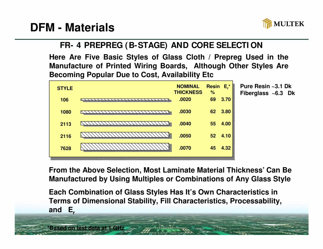
FR- 4 PREPREG (B-STAGE) AND CORE SELECTI ONHere Are Five Basic Styles of Glass Cloth / Prepreg Used in the Manufacture of Printed Wiring Boards, Although Other Styles AreBecoming Popular Due to Cost, Availability Etc
106
1080
2113
2116
7628
.0020 69 3.70
.0030 62 3.80
.0040 55 4.00
.0050 52 4.10
.0070 45 4.32
STYLE NOMINAL Resin Er* THICKNESS %
From the Above Selection, Most Laminate Material Thickness’ Can Be Manufactured by Using Multiples or Combinations of Any Glass Style
Each Combination of Glass Styles Has It’s Own Characteristics inTerms of Dimensional Stability, Fill Characteristics, Processability, and Er
Pure Resin ~3.1 DkFiberglass ~6.3 Dk
*Based on test data at 1 GHz
DFM - Materials
HDI Design
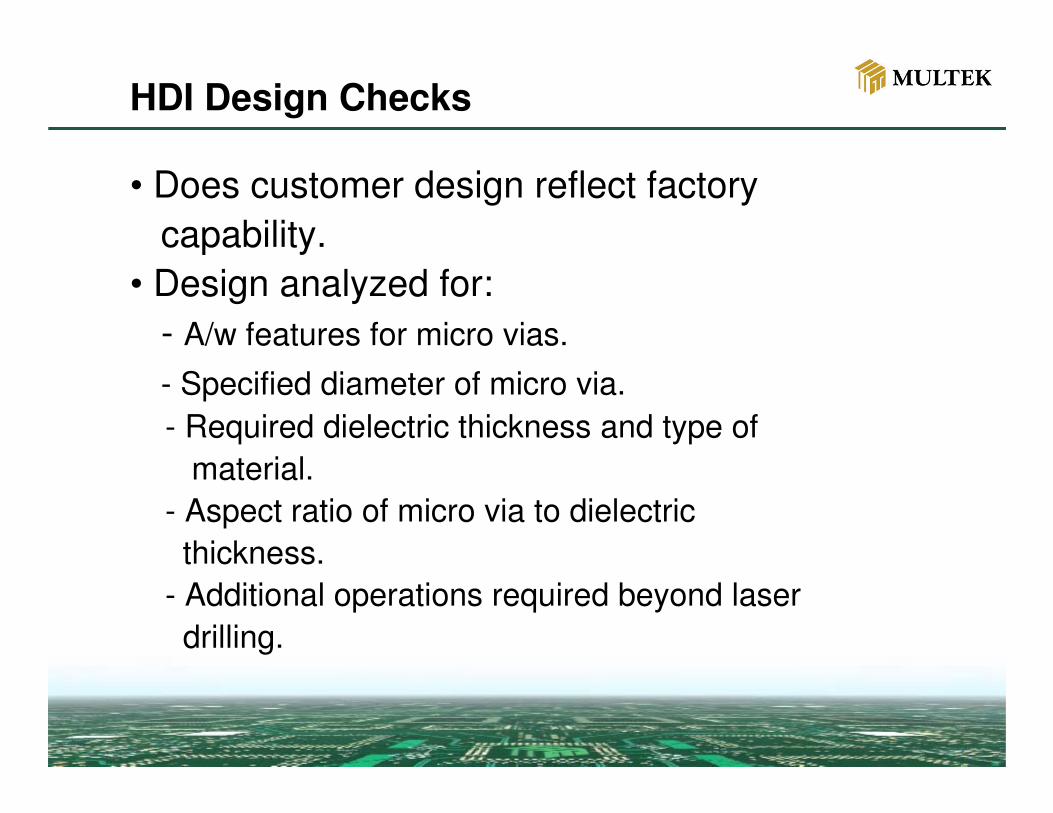
HDI Design Checks
• Does customer design reflect factory capability.
• Design analyzed for:- A/w features for micro vias.- Specified diameter of micro via. - Required dielectric thickness and type of
material.- Aspect ratio of micro via to dielectric thickness.
- Additional operations required beyond laserdrilling.
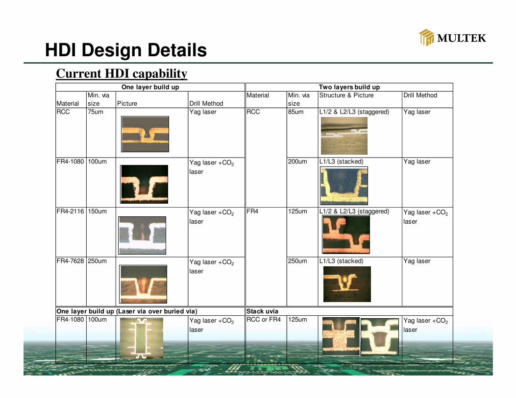
HDI Design Details
MaterialMin. viasize Picture Drill Method
Material Min. viasize
Structure & Picture Drill Method
RCC 75um Yag laser 85um L1/2 & L2/L3 (staggered) Yag laser
FR4-1080 100um Yag laser +CO2
laser
200um L1/L3 (stacked) Yag laser
FR4-2116 150um Yag laser +CO2
laser
125um L1/2 & L2/L3 (staggered) Yag laser +CO2
laser
FR4-7628 250um Yag laser +CO2
laser
250um L1/L3 (stacked) Yag laser
FR4-1080 100um Yag laser +CO2
laser
RCC or FR4 125um Yag laser +CO2
laser
One layer build up (Laser via over buried via)
One layer build up Two layers build up
RCC
FR4
Stack uvia
Current HDI capability
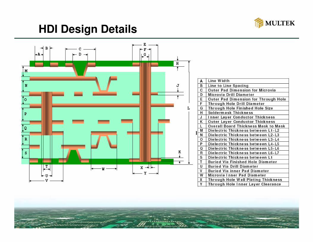
HDI Design Details
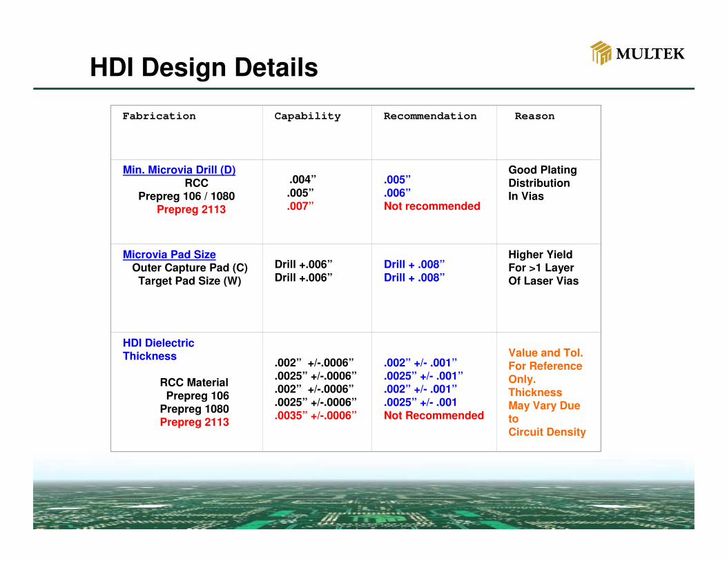
HDI Design Details
Fabrication Capability Recommendation Reason
Min. Microvia Drill (D)RCC
Prepreg 106 / 1080Prepreg 2113
.004”.005”.007”
.005”
.006”Not recommended
Good PlatingDistributionIn Vias
Microvia Pad Size Outer Capture Pad (C)
Target Pad Size (W)Drill +.006”Drill +.006”
Drill + .008”Drill + .008”
Higher YieldFor >1 LayerOf Laser Vias
HDI Dielectric Thickness
RCC MaterialPrepreg 106
Prepreg 1080Prepreg 2113
.002” +/-.0006”
.0025” +/-.0006”
.002” +/-.0006”
.0025” +/-.0006”
.0035” +/-.0006”
.002” +/- .001”
.0025” +/- .001”
.002” +/- .001”
.0025” +/- .001Not Recommended
Value and Tol.For ReferenceOnly. ThicknessMay Vary Due toCircuit Density
DFM Process
7KDQN�<RX��