Embed Size (px)
Citation preview
Design & Material Characterization for 3D Printing Sensor KAVYA1, ARIVARASI A1, ANAND KUMAR R1, JEGATHA NAMBI KRISHNAN2
Electrical & Electronics Department 1BITS - PILANI Dubai Campus / 2BITS-PILANI Goa Campus
International Academic City UNITED ARAB EMIRATES
[email protected];[email protected];[email protected];[email protected]
Abstract: - 3D printing requires constant innovation in materials for wider utilization. Sensor size impacts fabrication in a larger aspect and for printing the sensors effectively. Sensor performance measures include size, resolution, aspect ratio and response time. Speed has a tradeoff for resolution. The use of nano materials to develop electrochemical sensors has attracted growing interest in recent times. Enhanced chemical, physical, mechanical and electrical properties of nano materials coupled with the right technology make the sensing devices more efficient for key applications. The materials for 3D printed nano porous gold electrochemical sensor are analyzed and characterized. The nano porous gold film is fabricated by immersing copper in and chemically reacting with potassium gold cyanide solution at around 700C. The crude resistance value of copper prior to the chemical reaction is 0.94Ω. The resistance of the nanoporous gold film is 0.15Ω, 2 minutes after immersion in the potassium gold cyanide solution; the resistance does not change significantly after 6 hours of immersion. The porosity of the nano porous gold film is observed in a microscope to be 0.24% after 2 minutes of immersion. The porosity does not change with time during the process. The characterization of results is provided after experimentation. Key-Words: - copper, potassium gold cyanide, resistance measurement, nano porous gold 1 Introduction Nano sensors are very tiny devices capable of detecting and responding to physical stimuli having one billionth of a matter in meter dimensions. The physical stimulus could be biological, chemical substances, displacement, motion, force, mass, acoustic or thermal [2]. The sensor is able to sense the environmental properties at gaseous, liquid or extremely small solid property levels. The transducer converts the input to an electrical signal. The converted energy or the property is measured for the detected changes [14]. Metal nano particles have been used as enhancers of the electro analytical signal in different sensor architectures due to their electro catalytic properties [2]. Gold nano particles are utilized to enhance the improve the sensitivity of several kind of sensors [3]. Hybrid nano materials containing gold nano particles have been designed with the aim of enhancing the analytical response of electrochemical sensors and biosensors [2]. The wide variety of materials used currently for 3D printing are photopolymers, thermoplastic filaments, thermoplastic powders, metal powders, sand and binder, welding wire and plaster [1] [12]. The emerging materials
are biomaterials, carbon made of fiber, ceramics, graphene, electrically conducting materials, silicone and much more. Nano porous gold possess high material benefits for sensor applications due to its high surface area, high electrically conductivity and reduced stiffness [4]. Electrochemical sensors have the means to use nano porous gold fabricated using electro less plating method, which is of amperometric type. The amperometric type sensor results a current signal proportional to analyte proportion [5]. In electro less plating method, the substrate initiates autocatalytic chemical reduction process [29]. Resulting micro porous NPGF films can be characterized using a microscope [15]. The primary objective of the experimentation is to characterize, gather the material properties of the layers and inter-layer compatibility through theoretical and experimental means. The sensor can then be fabricated to detect heavy metal ions in water [14]. The requisite fluid properties like viscosity and surface tension are determined from literature. The sensor materials used for detection of heavy metal ions require to be layered in an accurate fashion with a precise resolution, wherein 3D
Kavya et al.International Journal of Circuits and Electronics
http://www.iaras.org/iaras/journals/ijce
ISSN: 2367-8879 128 Volume 1, 2016
printing technology is utilized. Experiments are conducted with the bath properties of appropriate chemical compositions in order to 3D print. 2 Sensor materials and structure for heavy metal ion detection In literature, the gold nanoparticle probes in environmental analysis include chemical sensing to detect heavy metal ions [9]. The 3D printable water quality sensor includes a printed copper layer on a suitable substrate, above which the nanoporous layer is formed. Nanoporous gold containing small pores having few nano meter size tiny pores involves a highly selective process with metal dealloy / reduction process, applied for fabricating / printing nano sensors [13]. The water quality sensor contains a layering structure where on a base substrate, copper is deposited to spray PGC solution in order to form nanoporous gold. Titanium epoxy is used as an adhesive to hold the copper to the substrate. Titanium has a low coefficient of thermal expansion compared to other usable substrates and possesses very low electrical conductivity. Hence it is suitable as an adhesive above a substrate. Titanium epoxy bonds well with metal, copper and semi conductor wafers. The 3D printed copper layer is formed by printing and sintering nano copper ink. The nano copper ink is prepared by mixing copper nano particles in a proportionate solution. The sintering takes place at about 700C. Melting temperature of nano particle is of considerable interest for sintering [11] [19] [26]. Copper is corrosion resistant. Oxygen free copper [6] is used above the titanium layer; both the copper and titanium layers are of nanometer thicknesses [7]. Both Poly Methyl Methacrylate (PMMA) and silicon are stable at this temperature and can be used as the substrate. PMMA and Silicon have similar coefficients of thermal expansion. PMMA maintains its properties even when exposed to sun and is a good dielectric, making it suitable for products intended for long open end air operation. Acrylics are unaffected by most laboratory chemicals, cleaners, acids and alkalis. Neither PMMA nor Silicon chemically react with titanium at the sintering temperature of 700C. Once the substrate, the titanium epoxy and sintered copper are 3D printed, the nano porous gold film (KAu(CN)2) can be formed by immersion in alkaline potassium gold cyanide (PGC) bath solution containing KAu(CN)2 [3] [7]. To 3D print the materials mentioned, the experimentation and characterization is required. The choice of substrate materials and subsequent layers is
analyzed for its inter layer compatibility. 2.1 Choice of substrate material and inter layer compatibility analysis The choice of materials for the layers requires thermal match, chemical match and lattice match to be maximized. The lattice of PMMA varies with temperature. 2.1.1 Thermal Match Interactions between PMMA and TiO2 nanoparticle molecules indicates changes in crystallinity/amorphosity ratio; miscibility is possible at higher temperatures. TiO2 increases the thermal stability of PMMA. PMMA is stable upto 1000C. Higher temperatures may lead to thermal degradation of the polymer. The substrate is susceptible to radiation damage and it is not advisable to operate at greater than 2000C. Stable bonds are formed with Si substrate. The lattice structure variations are minimal with a Silicon substrate. Polished silicon wafers with the following specifications is used as a substrate: 200 mm thickness, 8" diameter, phosphorus or boron doping, 1 - 60 ohm resistivity, (100) crystalline plane. Titanium epoxy bonds well with metal, copper and semi conductive wafers. Dark gray color, waterproof formula can handle temperatures from -600F to +2000F. Equal proportion of the hardener and resin can be mixed for 4 to 8 hours. Heat is generated while the epoxy mixture cures. The more the quantity of hardener and resin, the more the heat that is generated causing the epoxy mixture to cure faster. Normally, the hardener and resin are used in equal proportions. At 3500C, amorphous layer is formed at the interface, at 4000C, diffusion takes place and no oxygen is detected [33]. At 5000C, titanium silicide is formed [32]. Silicon with Titanium layer possesses a higher thermal stability than PMMA substrate with titanium combination of layering. 2.1.2 Chemical match
Titanium on PMMA is chemically inert for up to 1000C. For Silicon with Titanium, it is noted that an amorphous layer is formed at the interface at 3500C [18]. When the layer temperature reaches 4000C, silicon diffuses into titanium. When heated to 5000C, titanium silicide is formed. TiSi2 is formed over a small temperature range [6]. At higher temperatures, TixSiy, C49-TiSi2 are formed [31]. Copper is corrosion resistant. As per the analysis,
Kavya et al.International Journal of Circuits and Electronics
http://www.iaras.org/iaras/journals/ijce
ISSN: 2367-8879 129 Volume 1, 2016
chemical match is proved better for silicon being a base substrate for the titanium and copper deposits. 2.1.3 Lattice Match and analysis through Phase Transformation Crystallography Lab (PTC) tool For Titanium on PMMA, the crystalline structure changes when TiO2 is added. The lattice crystal structure of PMMA is redefined based on the heating temperature. It is determined that the lattice parameter indicate moderate expansion with the annealing temperature. The lattice distortion rate (Δa/a) is estimated to be between 0.60% and 0.013%. The highest distortion is obtained at 120°C. The geometric models for transformation crystallography is based on fit/misfit analysis of the atoms from two crystals. The closest distance between two atoms from the two crystals is defined as misfit value. The geometrical interface layer requires the misfit values to reach their minimum at the interface or growth direction [22]. Part of the mismatch is accommodated by misfit dislocations. The Phase Transformation Crystallography (PTC) tool allows to study the oriental and crystallographic properties of layer phase transformation [28]. Using a set of crystal information on Silicon and Titanium on PTC tool, the misfit information is calculated. OR matrix value is taken as input and three dimensional matching is analyzed. The deviation angle between the planes is used for description of oriental relationship [8]. The angle between planes or directions from the difference is calculated. The misfit between directions is calculated as length difference. Between Silicon and Titanium, the misfit is estimated to be 0.39nm, through the PTC (Phase transformation Crystallography) Lab tool. This indicates titanium layer to be more oriented with silicon in layering process, as the deviation is less than 9%. Compared to PMMA, silicon provides better match w.r.to thermal coefficient of expansion, chemical match, lattice match and strength. 3 PGC reaction with copper Elsner’s equation for cyanidation is seen in equation (1). Gold and cyanide mixed with oxygen and water produces gold cyanide with potassium hydroxide in equation. With sodium cyanide mixed with gold in aerated environment, produces sodium gold cyanide, as per equation (2).
!!!!!!!4!Au + 8!CN) + O+ + 2H+0!!!!!!!!!!!!!!!!!!!!= 4! Au CN + + 4!!OH) !!!!!!!!!!!!!!!!!!!!− ! 1 !!
!!!!!!!!!!!!!!!!!!!!!!!!!!!!!!!!!!!!!!!!!!!!!!!!!!!!!!!!!!!!!!!!!!!!!!!!!!!!!!!!!!!!!!!!!!!!!!!!!!!!!!!!!!!!!!!!!!!!!!!!!!!
!!!!!!!!!!!!!!!!!!!!!!!!!!!!!!!!!!!!
!!!4!Au + 8!NaCN +!O+ + !2H+O= !4!Na! Au CN + + !4!NaOH!! − (2)!
!Process! of! extracting! gold! from! ore! is! normally! termed!cyanidation.!Potassium!gold!cyanide!with!copper!reacts!to!provide! gold! cyanide,! cuprous! cyanide! and! potassium!cyanide.! The! reduction! process! of! gold! ions! takes! place!subsequently.! The! formation! of! nanoporous! gold! deposit!happens! on! copper,! which! is! proportional! to! time! and!percentage!of!Au!ions!in!solution.!The!reaction!rate!depends!on!the!temperature!provided.! !!!!!!4 K Au CN + + 2Cu = AuCN+! + 2Cu CN + + 2Au! +
!!!!!!!!!!!!!!!!!!!!!!!!!!!!!!!!!!!!!!!!!!!!!!!2KCN!!!!!!!!!!!!!!!!!!!!!!!!!!!!!!!!!!! − (3)
!!!!!!4[ K Au CN + + 2!Cu + 2H+O = 2Au CN + +!!!!!!!!!!!!!!!!!!!!!2Cu CN + + 2Au +!2OH) + 2KOH!!!!!!!!!!!!!! − (4)
Equation (3) and (4) theoretically implies the effect of copper on PGC. The gold undergoes reduction process. It is experimentally verified using a copper strip immersed in PGC solution, maintaining suitable temperature.
4 Experimental results In the experiment, a PGC solution of 15ml is prepared using 2.25g of PGC is made in a beaker and stirred with a glass rod till completely dissolved. The PGC solution is then heated in a digital water bath at 700C as shown in Fig.1. The test tube containing the PGC solution is indirectly heated in the bath. The PGC solution is heated for 2 minutes before immersing the Copper strip in the solution. The resistance of the copper strip is then measured. The resistance of the strip is also measured after 90 minutes and 6 hours of immersion [4]. The color of the copper strip was observed before the immersion and at the 2 minute, 90 minute and 6 hour instants. The color of the strip was also observed about 6 to 18 hours after removal from immersion and exposure to external environment.
TABLE 1 - EXPERIMENTAL RESULTS ON RESISTANCE MEASUREMENT OF COPPER STRIPS IMMERSED IN PGC SOLUTION FOR VARIED TIME PERIODS
Material used
Before immersi
on
Resistance measured in ohms after double layered heating of PGC solutiona
After 2 minutes
After 90 minutes After 6 hours
Copper Metal Strip
0.94Ω 0.15Ω 0.16Ω 0.14 Ω
a.!PGC solution maintained in alkaline medium pH
Kavya et al.International Journal of Circuits and Electronics
http://www.iaras.org/iaras/journals/ijce
ISSN: 2367-8879 130 Volume 1, 2016
The resistance measured over time indicates the increase in conductivity due to the formation of nano porous gold as per the microscopic structure. The conductivity increases significantly after the initial 2-minute immersion but does not change significantly after that. Two minutes after immersion in the heated PGC solution, the copper strip takes on a pinkish color. When heated for 90 minutes, the color turned brown and at 6 to 18 hours the greenish color showing oxidation is visible, when exposed to air. A vacuum desiccator cabinet is preferred to store the PGC dipped strip for further micro analysis, after is taken out of the solution. The reduction in resistance infers increase in conductivity of the copper surface top layer. The potassium gold cyanide reacts with copper surface to leave nanoporous gold in the surface after 6 hours of immersion. The conductivity is due to the porous and high surface nature of nanoporous gold, which is formed subsequently. Surface of a deposited or printed structure can be electrically measured using multimeter with good accuracy [26]. The digital multimeter is used to measure before and after immersion resistance values. The formation of nanoporous gold is seen through a microscope.
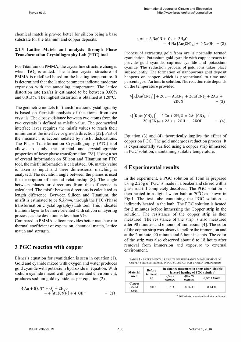
The double layered heating system used is provided in Fig. 1. Alkaline medium of pH is maintained while heating PGC, which provides high stable reaction rate.
Fig. 1 – Double layered heating system 5 Characterization of copper strip immersion through metallurgical microscope
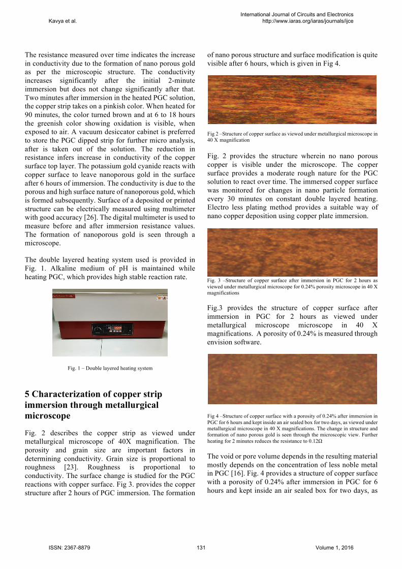
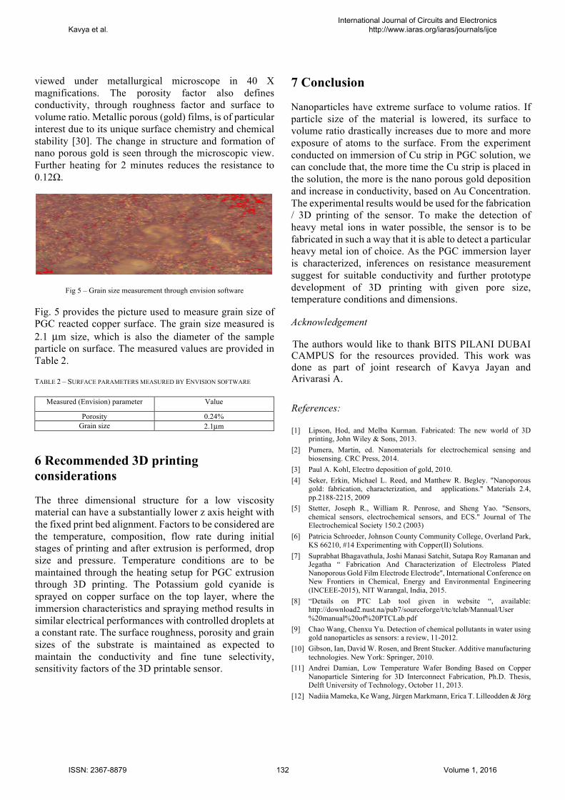
Fig. 2 describes the copper strip as viewed under metallurgical microscope of 40X magnification. The porosity and grain size are important factors in determining conductivity. Grain size is proportional to roughness [23]. Roughness is proportional to conductivity. The surface change is studied for the PGC reactions with copper surface. Fig 3. provides the copper structure after 2 hours of PGC immersion. The formation
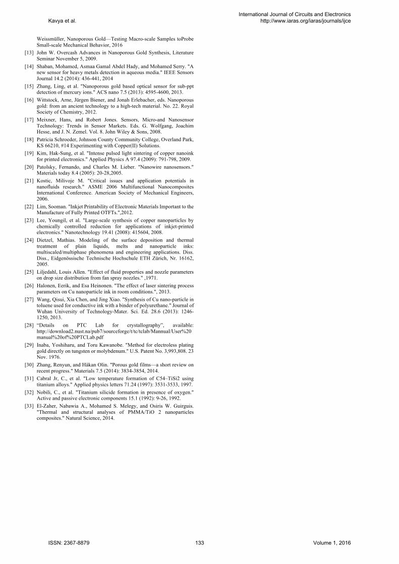
of nano porous structure and surface modification is quite visible after 6 hours, which is given in Fig 4.
Fig 2 –Structure of copper surface as viewed under metallurgical microscope in 40 X magnification Fig. 2 provides the structure wherein no nano porous copper is visible under the microscope. The copper surface provides a moderate rough nature for the PGC solution to react over time. The immersed copper surface was monitored for changes in nano particle formation every 30 minutes on constant double layered heating. Electro less plating method provides a suitable way of nano copper deposition using copper plate immersion.
Fig. 3 –Structure of copper surface after immersion in PGC for 2 hours as viewed under metallurgical microscope for 0.24% porosity microscope in 40 X magnifications
Fig.3 provides the structure of copper surface after immersion in PGC for 2 hours as viewed under metallurgical microscope microscope in 40 X magnifications. A porosity of 0.24% is measured through envision software.
Fig 4 –Structure of copper surface with a porosity of 0.24% after immersion in PGC for 6 hours and kept inside an air sealed box for two days, as viewed under metallurgical microscope in 40 X magnifications. The change in structure and formation of nano porous gold is seen through the microscopic view. Further heating for 2 minutes reduces the resistance to 0.12Ω The void or pore volume depends in the resulting material mostly depends on the concentration of less noble metal in PGC [16]. Fig. 4 provides a structure of copper surface with a porosity of 0.24% after immersion in PGC for 6 hours and kept inside an air sealed box for two days, as
Kavya et al.International Journal of Circuits and Electronics
http://www.iaras.org/iaras/journals/ijce
ISSN: 2367-8879 131 Volume 1, 2016
viewed under metallurgical microscope in 40 X magnifications. The porosity factor also defines conductivity, through roughness factor and surface to volume ratio. Metallic porous (gold) films, is of particular interest due to its unique surface chemistry and chemical stability [30]. The change in structure and formation of nano porous gold is seen through the microscopic view. Further heating for 2 minutes reduces the resistance to 0.12Ω.
Fig 5 – Grain size measurement through envision software
Fig. 5 provides the picture used to measure grain size of PGC reacted copper surface. The grain size measured is 2.1 µm size, which is also the diameter of the sample particle on surface. The measured values are provided in Table 2.
TABLE 2 – SURFACE PARAMETERS MEASURED BY ENVISION SOFTWARE
Measured (Envision) parameter Value
Porosity 0.24% Grain size 2.1µm
6 Recommended 3D printing considerations
The three dimensional structure for a low viscosity material can have a substantially lower z axis height with the fixed print bed alignment. Factors to be considered are the temperature, composition, flow rate during initial stages of printing and after extrusion is performed, drop size and pressure. Temperature conditions are to be maintained through the heating setup for PGC extrusion through 3D printing. The Potassium gold cyanide is sprayed on copper surface on the top layer, where the immersion characteristics and spraying method results in similar electrical performances with controlled droplets at a constant rate. The surface roughness, porosity and grain sizes of the substrate is maintained as expected to maintain the conductivity and fine tune selectivity, sensitivity factors of the 3D printable sensor.
7 Conclusion
Nanoparticles have extreme surface to volume ratios. If particle size of the material is lowered, its surface to volume ratio drastically increases due to more and more exposure of atoms to the surface. From the experiment conducted on immersion of Cu strip in PGC solution, we can conclude that, the more time the Cu strip is placed in the solution, the more is the nano porous gold deposition and increase in conductivity, based on Au Concentration.
The experimental results would be used for the fabrication / 3D printing of the sensor. To make the detection of heavy metal ions in water possible, the sensor is to be fabricated in such a way that it is able to detect a particular heavy metal ion of choice. As the PGC immersion layer is characterized, inferences on resistance measurement suggest for suitable conductivity and further prototype development of 3D printing with given pore size, temperature conditions and dimensions.
Acknowledgement
The authors would like to thank BITS PILANI DUBAI CAMPUS for the resources provided. This work was done as part of joint research of Kavya Jayan and Arivarasi A.
References: [1]! Lipson, Hod, and Melba Kurman. Fabricated: The new world of 3D
printing, John Wiley & Sons, 2013. [2]! Pumera, Martin, ed. Nanomaterials for electrochemical sensing and
biosensing. CRC Press, 2014. [3]! Paul A. Kohl, Electro deposition of gold, 2010. [4]! Seker, Erkin, Michael L. Reed, and Matthew R. Begley. "Nanoporous
gold: fabrication, characterization, and � applications." Materials 2.4, pp.2188-2215, 2009
[5]! Stetter, Joseph R., William R. Penrose, and Sheng Yao. "Sensors, chemical sensors, electrochemical sensors, and ECS." Journal of The Electrochemical Society 150.2 (2003)
[6]! Patricia Schroeder, Johnson County Community College, Overland Park, KS 66210, #14 Experimenting with Copper(II) Solutions.
[7]! Suprabhat Bhagavathula, Joshi Manasi Satchit, Sutapa Roy Ramanan and Jegatha “ Fabrication And Characterization of Electroless Plated Nanoporous Gold Film Electrode Electrode", International Conference on New Frontiers in Chemical, Energy and Environmental Engineering (INCEEE-2015), NIT Warangal, India, 2015.
[8]! “Details on PTC Lab tool given in website “, available: http://download2.nust.na/pub7/sourceforge/t/tc/tclab/Mannual/User %20manual%20of%20PTCLab.pdf
[9]! Chao Wang, Chenxu Yu. Detection of chemical pollutants in water using gold nanoparticles as sensors: a review, 11-2012.
[10]! Gibson, Ian, David W. Rosen, and Brent Stucker. Additive manufacturing technologies. New York: Springer, 2010.
[11]! Andrei Damian, Low Temperature Wafer Bonding Based on Copper
Nanoparticle Sintering for 3D Interconnect Fabrication, Ph.D. Thesis, Delft University of Technology, October 11, 2013.
[12]! Nadiia Mameka, Ke Wang, Jürgen Markmann, Erica T. Lilleodden & Jörg
Kavya et al.International Journal of Circuits and Electronics
http://www.iaras.org/iaras/journals/ijce
ISSN: 2367-8879 132 Volume 1, 2016
Weissmüller, Nanoporous Gold—Testing Macro-scale Samples toProbe Small-scale Mechanical Behavior, 2016
[13]! John W. Overcash Advances in Nanoporous Gold Synthesis, Literature Seminar November 5, 2009.
[14]! Shaban, Mohamed, Asmaa Gamal Abdel Hady, and Mohamed Serry. "A new sensor for heavy metals detection in aqueous media." IEEE Sensors Journal 14.2 (2014): 436-441, 2014
[15]! Zhang, Ling, et al. "Nanoporous gold based optical sensor for sub-ppt detection of mercury ions." ACS nano 7.5 (2013): 4595-4600, 2013.
[16]! Wittstock, Arne, Jürgen Biener, and Jonah Erlebacher, eds. Nanoporous gold: from an ancient technology to a high-tech material. No. 22. Royal Society of Chemistry, 2012.
[17]! Meixner, Hans, and Robert Jones. Sensors, Micro-and Nanosensor Technology: Trends in Sensor Markets. Eds. G. Wolfgang, Joachim Hesse, and J. N. Zemel. Vol. 8. John Wiley & Sons, 2008.
[18]! Patricia Schroeder, Johnson County Community College, Overland Park, KS 66210, #14 Experimenting with Copper(II) Solutions.
[19]! Kim, Hak-Sung, et al. "Intense pulsed light sintering of copper nanoink for printed electronics." Applied Physics A 97.4 (2009): 791-798, 2009.
[20]! Patolsky, Fernando, and Charles M. Lieber. "Nanowire nanosensors." Materials today 8.4 (2005): 20-28,2005.
[21]! Kostic, Milivoje M. "Critical issues and application potentials in nanofluids research." ASME 2006 Multifunctional Nanocomposites International Conference. American Society of Mechanical Engineers, 2006.
[22]! Lim, Sooman. "Inkjet Printability of Electronic Materials Important to the Manufacture of Fully Printed OTFTs.",2012.
[23]! Lee, Youngil, et al. "Large-scale synthesis of copper nanoparticles by chemically controlled reduction for applications of inkjet-printed electronics." Nanotechnology 19.41 (2008): 415604, 2008.
[24]! Dietzel, Mathias. Modeling of the surface deposition and thermal treatment of plain liquids, melts and nanoparticle inks: multiscaled/multiphase phenomena and engineering applications. Diss. Diss., Eidgenössische Technische Hochschule ETH Zürich, Nr. 16162, 2005.
[25]! Liljedahl, Louis Allen. "Effect of fluid properties and nozzle parameters on drop size distribution from fan spray nozzles." ,1971.
[26]! Halonen, Eerik, and Esa Heinonen. "The effect of laser sintering process parameters on Cu nanoparticle ink in room conditions.", 2013.
[27]! Wang, Qisui, Xia Chen, and Jing Xiao. "Synthesis of Cu nano-particle in toluene used for conductive ink with a binder of polyurethane." Journal of Wuhan University of Technology-Mater. Sci. Ed. 28.6 (2013): 1246-1250, 2013.
[28]! “Details on PTC Lab for crystallography”, available: http://download2.nust.na/pub7/sourceforge/t/tc/tclab/Mannual/User%20manual%20of%20PTCLab.pdf
[29]! Inaba, Yoshiharu, and Toru Kawanobe. "Method for electroless plating gold directly on tungsten or molybdenum." U.S. Patent No. 3,993,808. 23 Nov. 1976.
[30]! Zhang, Renyun, and Håkan Olin. "Porous gold films—a short review on recent progress." Materials 7.5 (2014): 3834-3854, 2014.
[31]! Cabral Jr, C., et al. "Low temperature formation of C54–TiSi2 using titanium alloys." Applied physics letters 71.24 (1997): 3531-3533, 1997.
[32]! Nobili, C., et al. "Titanium silicide formation in presence of oxygen." Active and passive electronic components 15.1 (1992): 9-26, 1992.
[33]! El-Zaher, Nabawia A., Mohamed S. Melegy, and Osiris W. Guirguis. "Thermal and structural analyses of PMMA/TiO 2 nanoparticles composites." Natural Science, 2014.
�
�
� �
Kavya et al.International Journal of Circuits and Electronics
http://www.iaras.org/iaras/journals/ijce
ISSN: 2367-8879 133 Volume 1, 2016