Embed Size (px)
Citation preview
International Journal of Scientific and Research Publications, Volume 4, Issue 8, August 2014 1 ISSN 2250-3153
H
Design of 32Bit Carry-lookahead Adder using
Constant Delay Logic K.Santosh
*, Sri G.Ramesh
**
* Department of ECE, G.PullaReddy Engineering College
** Department of ECE, G.PullaReddy Engineering College
Abstract - This paper presents an enhanced 32-bit carry look-
ahead(CLA) adder implementing using the constant delay (CD)
logic, targeting at full-custom high-speed applications. The CD
characteristic of this logic style regardless of the logic type
makes it suitable in implementing complicated logic
expressions such as addition. CD logic exhibits a unique
characteristic where the output is pre-evaluated before the
inputs from the preceding stage is ready. This feature offers
performance advantage over static and dynamic domino logic
styles in a single-cycle multistage circuit block. Several design
considerations including timing window width adjustment and
clock distribution are discussed. Using 65-nm general-purpose
CMOS technology, the proposed logic demonstrates an average
speed up of 94% and 56% over static and dynamic domino
logic, respectively, in five different logic gates. Simulation
results of 8-bit ripple carry adders show that CD logic is 39%
and 23% faster than the static and dynamic-based adders,
respectively. CD logic also demonstrates 39% speedup and
64%(22%) energy-delay product (EDP) reduction from static
logic at 100% (10%) data activity in 32-bit carry look ahead
adders. For 8-bit Wallace tree multiplier, CD logic achieves a
similar speedup with at least 50% EDP reduction across all data
activities.
Index Terms- Adder, constant delay (CD), feed through,
high-performance logic style, pre-evaluated.
I. INTRODUCTION
IGH-PERFORMANCE energy-efficient logic style has
always been a popular research topic in the field of
VLSI circuits because of the continuous demands of ever-
Increasing circuit operating frequency. The invention of the
dynamic domino logic [Fig. 1(a)] in the 1980s is one of the
answers to this request, as it allows designers to implement
high-performance circuit blocks, i.e., arithmetic logic units, at
an operating frequency that traditional static and pass transistor
CMOS logic styles find difficult to achieve [1]. However, the
performance enhancement comes with several costs, including
a reduced noise margin, a problem of charge-sharing and
higher power dissipation due to a higher data activity. Several
variations of the dynamic domino logic, namely NP domino
(NORA domino) [2], zipper domino [3], and data-driven
dynamic logic ( D3 L) [4], [5], have been proposed but they
are never widespread in the VLSI industry [6], [7].
Compound domino logic (CDL), where dynamic and static
gates alternating between each other, has become the most
Popular logic style in high-performance circuit blocks, i.e.
64-bit adder, in modern CPUs [8] – [11]. In this design, the
output inverter is replaced with a more complex inverting
static gate, i.e., NAND, such that the monotonicity require-
ment is satisfied while conducting complex logic operations
without wasting the one inverter delay [12]. Moreover, all
the dynamic stages except the first stage can be footless in
CDL. This implementation, however, comes at the expense of:
1) Increased power consumption due to the possible direct path
current during the precharge period; and 2) a reduced noise
margin as a result of unprotected dynamic domino logic’s
outputs [6].
A significant research effort has been dedicated to exploring
New logic styles that go beyond dynamic domino logic and
CDL. In particular, source-coupled logic (SCL) [13] has shown
superior performances that are difficult to achieve by any other
logic styles. However, it suffers from high power dissipation
due to a constant current draw, and its differential nature
requires complementary signals. Pseudo-nMOS logic, which
uses a single pull-up pMOS transistor, provides both high
speed and low transistor count at the expense of high static
power consumption as well as reduced output voltage swing.
Output prediction logic (OPL) [14] has also shown superior
performance in high-speed adders [15]. Nevertheless, OPL
requires the generation and distribution of multiphase clock
signals with small timing separations and low skews, which are
difficult to achieve. While numerous high-speed logic styles
have been proposed, dynamic and CDL still remain the most
attractive choices when performance is the primary concern.
In recent years, a new way of logic operation, also known as
feedthrough logic (FTL) [16], [17], has been proposed, which
has demonstrated its high-performance capability. Consider
dynamic domino logic [Fig. 1(a)], the critical path consists of
nMOS logic transistors. In FTL however, the roles of the clock
and logic transistors are interchanged (Section II-A) and the
clock transistor is now the critical path. The first generation of
FTL exhibits many shortcomings, including excessive power
dissipation, and reduced noise margin. To mitigate these prob-
lems, we propose a new high-performance logic, which we call
“constant delay” (CD) logic. CD logic provides a local window
technique and a self-reset circuit which enable robust logic
operation with minimized power consumption while maintain-
ing FTL’s speed advantage. The most distinct characteristic of
CD logic from previously proposed logic styles is that the
delay is, on a first-order approximation, not affected by the
logic expression.1 Unlike SCL, CD logic does not require
1 The delay of CD logic is still a function of logic expression when all effects are considered, since a more complicated logic expression implies a larger capacitive load.
International Journal of Scientific and Research Publications, Volume 4, Issue 8, August 2014 2 ISSN 2250-3153
(V)
CLK
IN
PDN
CLK
M1
Out
1.0
.75
.5
CLK
CLK
N1
N2 N3
N4
CLK
CLK N3
CLK
CLK
NMOS IN
Pull Down M2
Network
.25
0
N2 N4 N6 N8 M3 M2
(a)
(b) 575 600 625 650 675 700 725
time(ps)
Fig. 1. Schematic of (a) dynamic domino logic with a footer transistor and (b) FTL.
complementary signals and can be easily integrated with static
and dynamic domino logics. Also, CD logic does not have
the problem of constant static power dissipation similar to
pseudo-nMOS. Furthermore, the clock timing requirement of
CD logic is not as stringent as OPL. CD logic can achieve
robust operation with optimal performance as long as clock
signals arrive earlier than the input signals. In this paper, we
will demonstrate that: 1) CD logic outperforms other logic
styles with better energy efficiency and is particularly suitable
for high-performance digital blocks and 2) CD logic is robust
under extreme process and temperature variations.
The rest of this paper is organized as follows. Section II
reviews the history of FTL and introduces the proposed CD
logic. Section III discusses the design considerations of CD
logic and provides a first-order approximation of the unwanted
glitch voltage. Section IV analyzes the impacts of window
width on robustness and compares CD logic with other logic
styles in different logic expressions. Section V demonstrates
CD logic’s performance advantage in single-cycle multistage
digital applications such as 32-bit adders. Finally, Section VI
concludes with some final remarks.
II. EVOLUTION OF CD
LOGIC
A. FTL Logic
FTL logic [Fig. 1(b)] in CMOS technology was first intro-
duced in [16] and [17]. Its basic operation is as follows: when
CLK is high, the predischarge period begins and Out is pulled
down to GND through M2. When CLK becomes low, M1
is on, M2 is off, and the gate enters the evaluation period.
If inputs (IN) are logic “1,” Out enters the contention mode
where M1 and transistors in the nMOS pull-down network
(PDN) are conducting current simultaneously. If PDN is off,
then the output quickly rises to logic “1.” In this case, FTL’s
critical path is always a single pMOS transistor.
Despite its performance advantage, FTL suffers from
reduced noise margin, excess direct path current, and nonzero
nominal low output voltage, which are all caused by the
contention between M1 and nMOS PDN during the evaluation
period. Furthermore, cascading multiple FTL stages together
to perform complicated logic evaluations is not practical.
Consider a chain of inverters implemented in FTL cascaded
together and driven by the same clock, as shown in Fig. 2.
When CLK is low, M1 of every stage turns on, and the output
of every stage begins to rise. This will result in false logic
Fig. 2. Simulated unwanted glitch at different logic depths in a chain of inverters implemented with FTL.
evaluations at even numbered (i.e., 2, 4, 6, etc.,) stages since
initially there is no contention between M1 and nMOS PDN
because all inputs to nMOS transistors are reset to logic “0”
during the reset period.
B. CD Logic
To mitigate the above-mentioned problems, CD logic is
proposed with a schematic shown in Fig. 3(a). Timing block
(TB) creates an adjustable window period to reduce the static
power dissipation. Logic Block (LB) helps to reduce the
unwanted glitch and also makes cascading CD logic feasible.
A buffer implemented in CD logic with schematics of TB and
LB is shown in Fig. 3(b).
1) CD Logic Operation: Fig. 4 depicts the corresponding
CD logic timing diagram and flowchart. For simplicity, we
assume that IN come from dynamic domino logic gates. When
CLK is high, CD logic predischarges both X and Y to GND.
When CLK is low, CD logic enters the evaluation period and
three scenarios can take place: namely, the contention, C–Q
delay, and D–Q delay modes. The contention mode happens
when CLK is low while IN remains at logic “1.” In this case, X
is at a nonzero voltage level which causes out to experience
a temporary glitch. The duration of this glitch is determined
by the local window width, which is determined by the delay
between CLK and CLK_d. When CLK_d becomes high, and
if X remains low, then Y rises to logic “1,” and turns off M1.
Thus the contention period is over, and the temporary glitch at
Out is eliminated. C–Q delay mode takes places when IN make
a transition from high to low before CLK becomes low. When
CLK becomes low, X rises to logic “1” and Y remains at logic
“0” for the entire evaluation cycle. The delay is measured by
the falling edge of both CLK and Out: hence the name C–Q
delay. D–Q delay mode utilizes the pre-evaluated characteristic
of CD logic to enable high-performance operations. In this
mode, CLK falls from high to low before IN transit, hence
X initially rises to a nonzero voltage level. As soon as IN
become logic “0,” while Y is still low, then X quickly rises
to logic “1.” A race condition exists in this case between X
and Y. If CLK_d rises much earlier than X and Y will go to
logic “1,” turn off M1, and result in a false logic evaluation. If
CLK_d rises slightly slower than X, then Y will initially rise
(thus slightly turns off M1) but eventually settle back to logic
“0.” CD logic can still perform the correct logic operation
in this case, however, its performance is degraded because of
M1’s reduced current drivability. Therefore, it is important to

International Journal of Scientific and Research Publications, Volume 4, Issue 8, August 2014 3 ISSN 2250-3153
Timing
Block Y
B
M
INV1 INV2 INV3 2.8u
M1
X
IN
NMOS
Pull Down
Logic
lock
2
Out
CLK M3
X M4
CLK X
CLK_d
Y
Y 2.8u
M1 X
IN
1u
Logic Block
Out
CLK
Network M5 M6 M7 M2
Timing Block NMOS Pull Down Network
(a)
(b)
Fig. 3. CD logic (a) block diagram and (b) buffer.
CLK
CLK_d
Window Width C-Q Delay D-Q Delay CLK is high. X is predischarged to GND and
CLK is low, evaluation period
begins
(IN = “1”)
C-Q Delay Mode
discharges to GND
Yes, direct path current between
PMOS and PDN
IN X rises to a non-zero voltage
and conditionally transit to “0”
Contention
X
Y
Pre-evaluated
level, Out experiences a
temporary glitch
PDN is on for the entire
evaluation period ?
Contention Mode
while window is still
transparent (Y = 0)
prior or during the evaluation
period
X rises to logic “1”, Out
discharges to GND
Yes, remain in contention mode
Out Temporary
Glitch
eliminates temporary glitch
for the entire evaluation
period
Fig. 4. Timing diagram and flowchart of the proposed CD logic.
TABLE 1
SUMMARY OF CD LOGIC’S
OPERATION
Mode Scenario Operation
Predischarge CLK is high X and Out are predischarged and precharged to
GND and VDD, respectively.
Contention IN = “1” for the entire evaluation period. Direct path current flows from pMOS to PDN. X rises to a nonzero voltage level and Out
experiences a temporary glitch.
C-Q Delay IN goes to “0” before CLK transits to low. X rises to logic “1” and Out is
D-Q Delay IN goes to “0” after CLK transits to
low (while window is still open,
i.e., Y is still “0”).
Disacharged to VDD.
X initially enters contention mode
and later rises to logic “1.” Delay is
measured from IN to Out.
maintain a sufficient window width under process–voltage–
temperature (PVT) variations. Table I presents a summary of
CD logic’s operations.
Compared to FTL, where the contention lasts for the
entire evaluation period, TB effectively reduces CD logic’s
power consumption during the contention mode. The local
window technique in the proposed CD gate allows designers to
customize the window width for different logic expressions
to achieve minimal power dissipation while not sacrificing
the performance. For instance, a multiple input NAND
gate will require a longer window width than a NOR gate
because of the larger internal capacitance due to the stacked
nMOS transistors. Another advantage of CD logic is that the
internal node(X) is always connected to either VDD or GND,
thus making the robustness of CD logic comparable to static
logic, except during the contention mode.

International Journal of Scientific and Research Publications, Volume 4, Issue 8, August 2014
4 ISSN 2250-3153
Vss P1 P2
VDD-∆V2
VDD N1 N2
Fig. 5. Simplified schematic of CD logic during contention
mode
III. CD LOGIC DESIGN CONSIDERATIONS
A. CD Logic Sizing
The sizing of INV1-3 and M3–M6 in Fig. 3(b) is
close to the minimum size so that they do not create a huge
area burden. The length of INV1-3 can be altered to provide
the required timing window duration based on designer’s
choices.
1) CD Logic Versus Pseudo-nMOS: Both pseudo-nMOS and
CD logic are ratioed circuits which rely on the correct pMOS
to nMOS strength ratio to perform correct logic operations.
pMOS transistor width is often selected to be about one-
fourth the strength of the nMOS PDN as a compromise
between noise margin and speed in pseudo-nMOS [6]. On
the other hand, CD logic always discharges X to GND when
CLK is high, therefore, CD logic can be optimized for low-
to-high transition only. Hence, pMOS clock transistors in
CD logic can be upsized larger to provide more speedup, as
long as the output glitch is maintained at an acceptable level.
B. Output Glitch
Fig. 5 depicts a simplified schematic of CD logic
during the contention mode, where both transistors P1 and
N1 are on simultaneously and induce a glitch voltage _V1,
which in turn generates another smaller glitch ∆V2. By
design ,∆V1 should be small [i.e., less than the threshold
voltage (Vt )]. Hence,P1 operates in the saturation region
while N1 is in the linear region. The current equation is
given as
( )
=
[(
) ( )
] (1)
rearranging (1)
( )
( )
( )
(2)
V1 can be found by solving the quadratic equation
√( )
( )
(3)
By Taylor expansion, √
(4)
Assuming , (3) can be approximated as
( ) ( )
( )
( )
(5)
∆V2 can also be found through a similar approach. Consider
Fig. 5 again transistor N2 operates in the subthreshold region
while P2 is working in the linear mode. Equating the two
current equations yields.
( )
[( )
( )
] (6)
Where (18), (19)
( ) ,
,
(7)
Rearranging (6) gives
( )
( )
(8)
Where since ( ) >> . Solving
then yields
√( )
Applying taylors expansion
(( )
( )) (11)

International Journal of Scientific and Research Publications 5
Vo
lt a
ge (
mV
)
(V)
1. 03
1.0
.975
.95
.925
.9
.875
N1
N2 N3
N4 N5
Static logic has an empirical α of 0.1–0.2 [6] and dynamic
domino logic has an activity factor of 0.5. While CD logic’s
α is also 0.5, it always consumes power when it enters the
evaluation period. During the evaluation period, CD logic
always dissipates power via either dynamic power dissipation
(X goes to VDD and Out is discharged to GND) or direct path
current (contention mode). While CD logic consumes more
power, we believe that CD logic is still an attractive choice in 1.6 1. 65 1.7 1. 75
Time (ns)
Fig. 6. Simulated output glitch of a five-stage two-input AND gate implemented with CD logic.
100
AND3 - Aver age Glit ch 90
AND3 - 3σ
80 OR3 - Aver age Glit ch
70 OR3 - 3σ
60
50
40
30
20
10
0 -40 -20 0 20 40 60 80 100 120 140
Temper at ur e (°C)
Fig. 7. Temporary glitch mean and standard deviation at the output of three- input CD, AND, and OR gate versus temperature in a Monte Carlo simulation with 7500 iterations.
Finally
a high-performance full-custom design because: 1) CD logic
is only intended to replace the critical path; and 2) power
management techniques such as clock gating [20], [21], where
the clock connection to idle module is turned off (gated), will
significantly reduce CD logic’s dynamic power consumption.
D. CD Logic Family
CD logic’s LB [Fig. 3(a)] can be modified such that the
inverter is replaced by a static gate to achieve even higher
performance, since the inverter delay is not wasted. We refer
to such a variation as “compound CD logic” (CCD), analogous
to the case of CDL of the dynamic domino logic. Another
family of CD logic was proposed in [22], where the output
inverter is replaced by a dynamic domino logic. The analysis
in [22] shows that a 64-bit parallel-prefix adder employing
this type of logic is superior to its CDL-based counterpart,
however, it requires additional design considerations because
of the degraded noise margin.
IV. CD LOGIC CHARACTERIZATION
Unless otherwise specified, all simulation runs in this paper
V2 ≈ 2
V
V1−Vtn
Ae ηVT
V V
. (12)
are done in schematic level (transistor netlists), with extracted
parasitic capacitance in the Cadence design environment using
DD − 1 − t p
65-nm CMOS technology. All the CD logic gates are designed
Equations (5) and (12) provide several first-order design
insights for CD logic. For a given V1, designers can quickly
estimate the required W p1 to Wn1 ratio. Moreover, V1 is
linearly proportional to the shift of Vt and transistor width in
the presence of process variations. When V1 is sufficiently
small, V2 is approximately zero. As V1 increases, both
the numerator and denominator in 12 contribute to V2 ’s
exponential increase. In a multistage CD logic circuitry, V1
of each stage will slowly increase because of the reduced Vgs
of N1 due to V2 from the preceding stage. This phenomenon
is demonstrated in Fig. 6, where the glitch level aggravates as it
traverses through a series of two-input AND gate implemented
with CD logic. Equation (12) also suggests that V2 is a strong
function of temperature. Fig. 7 illustrates the mean and three
standard deviations (3σ ) of the temporary glitch at the output
of a three-input CD, AND, and OR gate versus temperature.
Clearly, as the temperature increases from 20 °C to 120 °C, the
3σ glitch level of a three-input AND gate raises from 55 mV
to approximately 140 mV.
C. Power Consumption
such that the worst case glitch level under 6σ deviation with
nominal VDD (1.0 V) is less than 300 mV at 110 °C. The
measured power consumption includes clock trees and data
buffers, which are both sized to drive a fanout-of-4 (FO4) load.
The outputs of all the logic gates are driving an identical 20 fF
load. The window duration (width) is defined as the 50% point
of the falling edge of CLK to the 50% point of the rising edge
of node Y. The delay is measured at the 50% switching point
of either the CLK or data to the 50% switching point of the
latest output.
In this section, all logic transistors have a 1-μm effective
nMOS width. For CD logic, the pMOS CLK transistors’
width is 2.4 μm. The transistor sizings are optimized primary
for delay, because the main objective of this section is to
explore CD logic’s performance advantage. The clock and data
frequencies are set to 2 GHz.
A. Noise Margin Versus Window Width
Noise margin is defined as the dc noise level at the input
generating a false logic evaluation at the output of the same
gate and can be computed based on the following formula:
Data activity measures how frequent signals toggle and is
defined as
Noise Margin = Voriginal − Vnoise (14)
where Voriginal is the expected voltage level without any inpu
International Journal of Scientific and Research Publications 6
N
ois
e M
arg
in (
mV
) N
orm
aliz
ed
Dela
y
No
ise M
arg
in (
mV
)
No
rma
lize
d A
vera
ge
P
ow
er
at
Various D
ata
Activity
10%
10%
10%
500
CD AND3 "0"-NM w/t keeper CD AND3 "0" NM w keeper CD OR3 "0" NM
Dynamic
800
600
400
27 10% 24 21 18 15 12
8
10%
400 CD OR3 "1" NM
AND3 NM 7 50% 6
50% 50% 50%
300
200
100
Dynamic OR3 NM
CD AND3 "1" NM w keeper CD AND3 "1"-NM w/t keeper
5
4 100%
3
2
1
100%
100%
100%
50%
100%
0 50 100 150 200 250 300
Window Duration (ps)
Fig. 8. Simulated logic “1” and “0” noise margin versus window duration for a three-input AND and OR gate.
AND2 AND3 OR2 OR3 AOI22
Static Dynamic CD
Fig. 10. Normalized average power of five logic expressions at various data activities implemented in static, dynamic, and CD logic.
1.1
1.0
0.9
0.8
0.7
0.6
0.5
0.4
0.3
AND2 AND3 OR2 OR3 AOI22
Static CD C-Q CD D-Q Dynamic
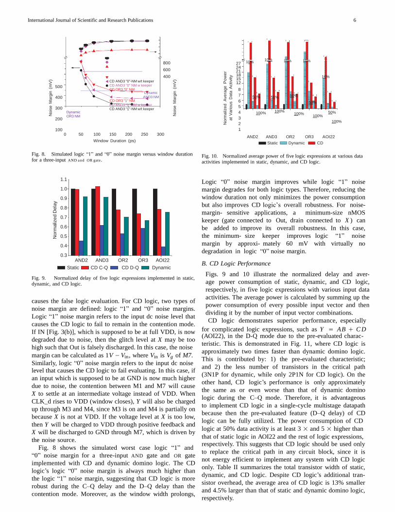
Logic “0” noise margin improves while logic “1” noise
margin degrades for both logic types. Therefore, reducing the
window duration not only minimizes the power consumption
but also improves CD logic’s overall robustness. For noise-
margin- sensitive applications, a minimum-size nMOS
keeper (gate connected to Out, drain connected to X ) can
be added to improve its overall robustness. In this case,
the minimum- size keeper improves logic “1” noise
margin by approxi- mately 60 mV with virtually no
degradation in logic “0” noise margin.
B. CD Logic Performance
Fig. 9. Normalized delay of five logic expressions implemented in static, dynamic, and CD logic.
causes the false logic evaluation. For CD logic, two types of
noise margin are defined: logic “1” and “0” noise margins.
Logic “1” noise margin refers to the input dc noise level that
causes the CD logic to fail to remain in the contention mode.
If IN [Fig. 3(b)], which is supposed to be at full VDD, is now
degraded due to noise, then the glitch level at X may be too
high such that Out is falsely discharged. In this case, the noise
margin can be calculated as 1V − Vin , where Vin is Vg of M7. Similarly, logic “0” noise margin refers to the input dc noise
level that causes the CD logic to fail evaluating. In this case, if
an input which is supposed to be at GND is now much higher
due to noise, the contention between M1 and M7 will cause
X to settle at an intermediate voltage instead of VDD. When
CLK_d rises to VDD (window closes), Y will also be charged
up through M3 and M4, since M3 is on and M4 is partially on
because X is not at VDD. If the voltage level at X is too low,
then Y will be charged to VDD through positive feedback and
X will be discharged to GND through M7, which is driven by
the noise source.
Fig. 8 shows the simulated worst case logic “1” and
“0” noise margin for a three-input AND gate and OR gate
implemented with CD and dynamic domino logic. The CD
logic’s logic “0” noise margin is always much higher than
the logic “1” noise margin, suggesting that CD logic is more
robust during the C–Q delay and the D–Q delay than the
contention mode. Moreover, as the window width prolongs,
Figs. 9 and 10 illustrate the normalized delay and aver-
age power consumption of static, dynamic, and CD logic,
respectively, in five logic expressions with various input data
activities. The average power is calculated by summing up the
power consumption of every possible input vector and then
dividing it by the number of input vector combinations.
CD logic demonstrates superior performance, especially
for complicated logic expressions, such as Y = AB + C D (AOI22), in the D-Q mode due to the pre-evaluated charac-
teristic. This is demonstrated in Fig. 11, where CD logic is
approximately two times faster than dynamic domino logic.
This is contributed by: 1) the pre-evaluated characteristic;
and 2) the less number of transistors in the critical path
(3N1P for dynamic, while only 2P1N for CD logic). On the
other hand, CD logic’s performance is only approximately
the same as or even worse than that of dynamic domino
logic during the C–Q mode. Therefore, it is advantageous
to implement CD logic in a single-cycle multistage datapath
because then the pre-evaluated feature (D–Q delay) of CD
logic can be fully utilized. The power consumption of CD
logic at 50% data activity is at least 3 × and 5 × higher than that of static logic in AOI22 and the rest of logic expressions,
respectively. This suggests that CD logic should be used only
to replace the critical path in any circuit block, since it is
not energy efficient to implement any system with CD logic
only. Table II summarizes the total transistor width of static,
dynamic, and CD logic. Despite CD logic’s additional tran-
sistor overhead, the average area of CD logic is 13% smaller
and 4.5% larger than that of static and dynamic domino logic,
respectively.

International Journal of Scientific and Research Publications 7
M0
2.8u
M1
2u
M 7
2u
8
0.3u
M 2
(V)
(V)
(V)
(V)
(V)
CLK1
0.5u
3u OUT1
CLK2
CLK_d
CLK2
CLK2
Y
2.8u
1u
A 3u
0.5u 20fF M3
X
M4 Y
X (OUT2_ ) 1.5u
OUT2
20fF
B 3u
CLK1 3u
CLK2 X A
M5 M6
B
M
CLK2
1.25
1.0
.75 B .5 A
.25
0
1.25
1.0
.75
.5
.25
0
-.25
CLK1
M02(27.756ps., 0005..00V))6ps
OUT1
1.25
1.0
.75
.5
.25
0
1.25
1.0
.75
.5
.25
0
-.25 1.25
1.0
.75
.5
.25
0
-.25
CLK2
A
B
Pre-evaluated
OUT2_
13.27ps
OUT2
1.1 1.15 1.2 1.25 1.3 1.35
time (ns)
(a)
1.325 1.35 1.375 1.400 1.425 1.45
time (ns)
(b)
Fig. 11. Schematic and timing waveform of (a) dynamic and (b) CD logic.
TABLE II
STAT I C , DYNAMI C , AND CD L OGI C AREA COMPA RI S O N
Total transistor width (μm) Number of transistors
Static Dynamic CD Static Dynamic CD
AND2 11 13.6 14.96 6 7 17
AND3 18 20.9 19.96 8 8 18
OR2 13 10.6 12.96 6 7 17
OR3 24 12.6 13.96 6 7 18
AOI22 27 19.6 18.96 10 9 19
Average 18.6 15.46 16.16 7.2 7.6 17.8
V. PE RFORMANCE ANALYSIS
A. 8-bit Ripple Carry Adders (RCAs)
The simulation setup in this section is similar to that of
Section IV. Three 8-bit RCAs using static, dynamic, and CD
logic style are simulated to compare their performances. An
RCA with FTL on the critical path is also implemented,
however, our analysis indicates that FTL-based RCA would
generate false outputs at the later bits because of the false
evaluation phenomenon described earlier. NP-FTL (equiva-
lent to NP-domino, where nMOS-FTL and pMOS-FTL alter-
nate) is also difficult to realize because the output glitch
is significant and easily exceeds 500 mV under process
variations.
The basic static full adder (FA) is implemented with 28 tran-
sistors with sizing strongly in favor of Cout computation [6].
The main purpose of this 8-bit RCA is to demonstrate CD
logic’s performance advantage and to discuss the design con-
siderations that should be taken into account when using CD
logic. A more energy-efficient pass-transistor FA design [23]
will be implemented in the subsequent analysis to provide a
more realistic comparison.
Only the timing-critical carry generation is replaced with
dynamic and CD logic, while noncritical sum computation
remains static in all three RCAs. Ten-thousand random input
vectors are applied to RCAs to compute the average power
consumption. The clock timing is designed in such a way that
all the CD logic gates except the first stage are operated in the
D–Q mode with a window duration of approximately 115 ps.2
Fig. 12(a) depicts the RCA block diagram and FA schematic.
Fig. 12(b) shows the corresponding worst case timing diagram
for CD logic, which occurs when {Cin , A0 · · · A7 , B0 · · · B7} = {0, 0 · · · 0, 1 · · · 1}.
1) Design Considerations in a Multistage System: Fig. 12(b)
provides several insights into designing single-cycle multistage
CD circuitries. When CD logic is to be used with other logic
styles and when the gate preceding the CD logic is not a
precharge type logic (i.e., dynamic domino logic), then the
inputs (Data) can only make transitions when all CD logic
gates are in the predischarge mode (i.e., CLK1–4 are high). CD
logic may suffer from additional power consumption due to
the possible direct path current during the predischarge mode.
Consider a CD-based RCA with the worst case input vector,
FA0-2’s CD logic carry circuitries enter predischarge mode
when CLK1 goes to high. The internal nodes before the output
inverter of all CD logic gates are all discharged to logic “0”
by nMOS clock transistors, and the outputs (C1 to C3 ) are
charged to logic “1.” If C3 becomes logic “1” before FA3
enters predischarge mode (i.e., CLK2 is still high), then a
direct path takes place.3 To avoid this condition, it is necessary
for Tdischarge ≥ Tdelta , where Tdischarge is the time that the CD logic takes to charge its output and Tdelta is the delay between two adjacent clock signals (CLK2 to CLK1, or CLK3
to CLK2, etc.).
2) CD Logic Sizing Strategy: To guarantee a 6σ glitch
level of 300 mV at 110 °C, the following sizing strategy is
employed.
1) An equally weighted variable is assigned to the width
of CD logic’s pMOS pull-up transistors.
2 The window duration is a function of the logic expression, the number of
preceding stages that are driving by the same phase clock signal, the maximum glitch level constraint, and the robustness of the overall system. Extensive simulation results have indicated that a window duration of 115 ps provides excellent delay and power performances while maintaining a sufficient timing margin against PVT and transistors mismatch variations (Table VII).
3 Consider the CD carry generation circuitry shown in Fig. 12(a), under
worst case vector condition B = 1 and A = 0. If input C (Cin from the
preceding stage) rises to logic “1” (originally at logic “0”) before CLK is high, then both pMOS and nMOS transistors are on.

International Journal of Scientific and Research Publications 8
FA7 ... FA1 S7 S1
Static
Data activity 10% 50% 100% Delay (ps) 369.4 (1.00)
C
C
3
1
B7 A7 CLK4
B1 A1
CLK1 B0 A0 CLK1
1 Cycle Time
C8 C1 FA0
Cin
S0 Critical Path CLK1
Tdelta
CD logic clock generation * Window period
CLK2 needs to arrive
CLK2 (FA3~4)
CLK1 (FA0~2)
CLK ≈ 115ps
* Clock and data
buffer power is
included
CLK2
CLK3
earlier than C3 Tdischarge
CLK3 (FA5~6) CLK4 (FA7)
Carry Generation
CLK4
CLK 1
Keeper 2 Cout
CLK 2.8
1 Cout
TB 2.8
C 3 A 1 1
t ≈ 115ps
Cout
1 Cout
2
A 3 B 3 B 1 CLK 0.3 C 2 A 2 2
CLK 3
Dynamic
C A 2 B 2 B 2 CD
C4 A 6 B 6 B 1
C 1
C 6 A 1 2 Cout
A 1 B 1 C 1 B 1 C5
Cout 1
1 Cout
A 1 S S C
C 3 A 1 1 A 1
6 0.5
A 3 B 3 B 1 Static B 1 C7 A 1 B 1 C
1 C 1
Sum Generation S8
(a)
(b)
Fig. 12. RCA (a) block diagram and (b) timing diagram implemented with CD logic.
TABLE III
RCA PERF O RMANCE COMPA RI S O N
Dynamic
10% 50%
292.6 (0.79
CD 100% 10% 50% 100%
) 224.4 (0.61) Power (μW) 50.95 254.77 509.54 142.70 336.05 401 231.85 533.96 602.82
Power–delay product (PDP) (fJ) 18.8 94.1 188.2 41.8 98.3 117.3 52 119.8 135 Energy–delay product (EDP) (fJ·ps) 6944 34761 69521 12231 28763 34322 11669 26883 30294
2) The entire circuitry (i.e., 8-bit RCA) is then simu-
lated under typical corner at 110 °C to determine the
glitch level. Extensive simulation results reveal that, if
this glitch level is approximately 65 mV, then the 6σ
glitch level will be less than 300 mV.
3) Iterative simulations are performed by sweeping this
variable until the glitch level is around 65 mV.
The equally weighted scheme clearly may not be the opti-
mal solution. However, different sizing schemes have been
explored and simulation results indicate that no apparent
performance improvement is achieved compared to the sizing
strategy described above.
3) RCA Performance: Table III compares static, dynamic,
and CD logic RCAs with various figures of merits at dif-
ferent data activity factors. CD-based RCA is approximately
39 and 23% faster than the static and dynamic counterparts,
respectively. On the other hand, the power consumption of CD
logic ranges from 4.55 × to 1.18 × higher than that of static
logic. In terms of the PDP, CD logic is 2.78 × more and 0.72 ×
B. 32-bit Carry Lookahead Adder (CLA)
We implement 32-bit CLAs to further analyze CD logic’s
performance. The detailed operations of CLA are described
in [6] and the schematic is displayed in Fig. 13. The 32-bit
CLA uses eight 4-bit FAs with dedicated circuitry to facilitate
carry generation. The energy-efficient FA used in this analysis
utilizes pass transistor logic styles with only 24 transistors for
sum generation [23]. For the carry generation, only the critical
path is replaced with different logic style. The maximum fan-
in is limited to four, except in the case of dynamic domino
logic due to the footer transistor. In this case, the 4-bit critical
carry generation path of CLA is
G3:0 = G3 + P3 (G2 + P2 (G1 + P1 (G0 ))) (15)
where G and P are the generate ( A · B ) and propagate ( A ⊕ B ) signals, respectively. CDL and CCD logic are implemented to reduce the number of fan-ins. One can utilize the inversion
property and rearrange 15 to
G1:0 = G1 + P1 G0 , P3:2 = P3 P2
less than static logic at 10 and 100% data activity, respectively. G3 2 = G
+ P G , G
= G ( P
+ G ). (16)
CD logic provides a speed advantage that logic styles such as : 3 3 2 3:0 3:2 3:2 1:0
static and dynamic find difficult to reach. Therefore, CD logic
is suitable in a system where performance is the most critical
factor.
Therefore, a maximum fan-in of two and three can be achieved
with CCD logic (Section III-D) and CDL, respectively. The
critical pMOS transistors’ width of CCD logic is slightly

International Journal of Scientific and Research Publications 9
0.5
C
1
1
1
P
CLK
1.2
TB
1.2
Compound CD
(CCD) logic*
* CCD logic replaces the inverter in the logic block with a complex logic gate to provide
better performance, similar to the idea of compound domino logic (CDL) over dynamic logic.
t ≈ 115ps G1+P1G0 CLK
CLK 0.3 G1 0.5 P1 1 3
1 0.3 3 G3:0 A B C
G 1 G3 1 P3 2.5 A A 1 1 1
CLK A B
G3+P3G2
4
G2 1.5 P2 2.5
0.3 2 0.5
B B 1 2
0.5
2 2
CLK 1.2
TB
1.2
G3:0 Dynamic logic G1 2
1 2.5 B P A
2 C C A B
P S
4 4 t ≈ 115ps
P3G2
G0 2.5 1
B 1
A 1
P 1
CLK 0.3 P3 1
P2 1
implemented with static
logic (not shown)
CLK 2.5 0.5
B
0.5
A
Sum Generation
0.5
C
S12:15 B12:15 A12:15 S8:11 B8:11 A8:11 S4:7 B4:7 A4:7 S0:3 B0:3 A0:3
C11 C7 C3
CLK
CLK
0.3 G3
TB
t ≈ 115ps
0.5 P3
1.4
1.4
2
1
G3:0
3
Critical Path
C31
G15:0, P15:0
G3 0.5 P3
0.25
2
2
G3:0
1
Cin
G2 1 P 2
G2 1
P2 2 2
CD logic
G1 1.5
P1 2
G0 2
G31:28
, P31:28 G27:0 , P27:0
G1
Pseudo-NMOS
1.5 P1 2
G0 2
C27 C23 C19 C15
S28:31 B28:31 A28:31 S24:27 B24:27 A24:27
S20:23 B20:23 A20:23
S16:19 B16:19 A16:19
Fig. 13. 32-bit CLA.
TABLE IV
32-BI T CL A PERF O RMANCE COMPA RI S O N
Data act ivity
Delay
Power 100%
PDP
EDP
Power 50%
PDP
EDP
Power 25%
PDP
EDP
Power 10%
PDP
EDP
Worst case (ps) (mW) (pJ) (pJ·ps) (mW) (pJ) (pJ·ps) (mW) (pJ) (pJ·ps) (mW) (pJ) (pJ·ps) leakage (μA)
Static 448 (1.00) 5.13 2.3 1030 1.94 0.87 390 0.99 0.45 199 0.42 0.19 85.1 32.9 Dynamic 316 (0.71) 5.27 1.67 526 2.22 0.7 222 1.32 0.42 132 0.8 0.25 79.8 32.1
CDL 287 (0.64) 5.29 1.52 437 2.21 0.63 182 1.33 0.38 110 0.81 0.23 66.7 32.7 Pseudo-nMOS 313 (0.70) 5.34 1.67 523 2.21 0.69 216 1.25 0.39 122 0.68 0.21 66.3 551.2
CD logic 272 (0.61) 5.02 1.37 371 2.31 0.63 171 1.43 0.39 106 0.90 0.25 66.8 33.5 CCD logic 239 (0.53) 5.09 1.22 291 2.34 0.56 134 1.46 0.35 84 0.94 0.22 53.5 33.4
smaller than that of CD logic to satisfy the 300-mV glitch
constraint because the pull-up path in the LB now consists of
two pMOS transistors. Footless dynamic domino logic cannot
be applied in this analysis because not all the circuits are
implemented with dynamic domino logic. Therefore, some of
the inputs to the dynamic domino logic in the critical path
can come from noncritical static gates. In order to satisfy
the monotonicity requirement and to avoid the possible direct
path current, a footer transistor is required for all dynamic
domino logics. On the other hand, if the entire 32-bit CLA
is implemented with dynamic domino logic, then the footless
scheme can be applied. However, simulation results indicate
that the power consumption in this case is much higher than
that of the current setup, thus making it a less attractive design.
Table IV summarizes the simulation results for the 32-bit
CLAs. Power consumption is calculated with 5000 random
input vectors. The performance enhancement of CD and CCD
logic is evident in this case, with 39 and 47% speedup over
static design, respectively. Both CD and CCD logic are also
faster than pseudo-nMOS, primarily because of the larger
effective pMOS width. The worst case leakage of all the
designs is comparable except the case of pseudo-nMOS, which
is caused by the contention between nMOS PDN and the weak
pMOS pull-up transistor. In this case, pseudo-nMOS’s leakage
(static power dissipation) is at least 15 × higher than the rest of the designs.
Figs. 14–16 show the normalized power, PDP, and EDP of all the CLAs analyzed in this paper, respectively. At 10%
(100%) α, the power consumption of CD logic is 2.1× (1.05×) Higher than the static logic.

International Journal of Scientific and Research Publications 10
1 S15 S14 S13 S12 S11 S10 S9 S8 S7 S6 S5 S4 S3 S2 S1 S0
DFF
0.9 0.8 0.7 0.6 0.5
100% 50%
25% 10%
Norm
aliz
ed E
DP
N
orm
aliz
ed P
DP
N
orm
aliz
ed P
ow
er
Norm
aliz
ed P
ow
er
2.3 2.2 2.1 2.0 1.9 1.8 1.7 1.6 1.5 1.4 1.3 1.2
Static
Dynamic
CDL
pseudoNMOS
CD logic
CCD logic
DFF CLK
Wallace
Tree
Critical path implemented
with various logic styles
Static logic only
1 Bit FA
1 Bit FA
1 Bit FA
1 Bit FA
1.1 1.0 0.9 0.8
100% 50% 25% 10%
Data Activity Factor
2:1 Mux
4 Bit FA
2:1 Mux
P8P7P6
Critical
Path
P12P11P10P9
Fig. 14. Normalized power of 32-bit CLAs.
DFF
CLK
3 Bit FA
1.5
1.4
1.3
1.2
1.1
1.0
Static
Dynamic
CDL
pseudoNMOS
CD logic
CCD logic
1 Bit Carry-bypass Adder
CLK
Fig. 17. 8-bit Wallace tree multiplier.
1.5
Static
1.4
1.3
Dynamic
pseudoNMOS
CD logic
1.2
1.1
Data Activity Factor
Fig. 15. Normalized PDP of 32-bit CLAs.
1.8
1.0
0.9
0.8
100% 50% 25% 10%
1.7 1.6 1.5 1.4 1.3 1.2 1.1 1.0 0.9 0.8 0.7 0.6 0.5 0.4 0.3 0.2
Static
Dynamic
CDL
pseudoNMOS
CD logic
CCD logic
100% 50% 25% 10%
Data Activity Factor
Data Activity Factor
Fig. 18. Normalized power of 8-bit multipliers.
TABLE V
CD AND CCD L OGI C GLI TCH I N 32-bit CL AS
CD logic CCD logic
Temp. Mean σ Mean + Mean σ Mean + (°C) (mV) (mV) 6σ (mV) (mV) (mV) 6σ (mV)
85 65.3 23.2 204.5 63.6 26.2 220.8
110 88.5 29.8 267.3 86.8 36.1 303.4
Fig. 16. Normalized EDP of 32-bit CLAs.
at 10%. While higher than CCD logic, the PDP of CD logic is
comparable to CDL and pseudo-nMOS and is lower than the
rest of the designs. At 25% α, EDP reduction of CD and CCD
logic from other designs is at least 4 and 24%, respectively.
At 10% data activity, CCD logic achieves the lowest EDP with
at least 19% improvement. Notice that the power consumption
of a CLA implemented with CD logic is lower than that of a
CLA with dynamic domino logic at 100% data activity. This
is because the width (1 μm) of CD logic’s pull-up pMOS
transistors in this CLA is much smaller than that (2.4 μm,
Section IV) of CD logic in a single-stage logic gate. Hence
the power consumption of dynamic domino logic is higher
than that of CD logic due to the higher internal capacitance
at 100% data activity. Similar reasoning can easily apply to a CLA with CCD logic.
Table V summarizes the mean and σ of CD and CCD
logic’s worst glitch level in a Monte Carlo simulation with
2000 samples. The worst case glitch is calculated by summing
up the mean and the extrapolated sixσ deviation.4 CCD logic
exhibits higher worst case glitch level than CD logic at both
85 °C and 110 °C, despite its already lower critical pMOS
effective width. Both designs are approximately within the
glitch constraint set earlier, and demonstrate that they are
still able to function properly under extreme process and
temperature conditions.
4 It is assumed that the glitch variation as a result of process variations follows Gaussian distribution.

International Journal of Scientific and Research Publications 11
Norm
aliz
ed P
DP
Norm
aliz
ed E
DP
TABLE VI
8-bit MULTI P L I E R PERF O RMANCE COMPA RI S O N
Data activity 100% 50% 25% 10%
Delay
(ps) Power
(mW) PDP
(pJ) EDP
(pJ·ps) Power
(mW) PDP
(pJ) EDP
(pJ·ps) Power
(mW) PDP
(pJ) EDP
(pJ·ps) Power
(mW) PDP
(pJ) EDP
(pJ·ps) Worst case
leakage (μA) Static 404 (1.00) 3.52 1.42 575 2.29 0.93 375 1.29 0.52 211 0.67 0.27 109 88.78
Dynamic 294 (0.73) 3.57 1.05 309 2.36 0.7 205 1.39 0.41 121 0.80 0.23 69 89.09 Pseudo-nMOS 292 (0.72) 3.82 1.11 325 2.56 0.75 218 1.57 0.46 134 0.96 0.28 82 619.6
CD logic 243 (0.60) 3.59 0.87 212 2.46 0.60 145 1.49 0.36 88 0.88 0.22 52 89.99
TABLE VII
PVT AND MONTE CARLO PERF O RMANCE ANA LY S I S O F T H E CD AND CCD L OGI C -BAS ED DES I GNS
Corner
Temperature (°C)
110
FF
−30
110
FS −30
110
SF
−30
110
SS −30
Monte Carlo
VDD (V) 1.1 0.9 1.1 0.9 1.1 0.9 1.1 0.9 1.1 0.9 1.1 0.9 1.1 0.9 1.1 0.9 mean σ 8-bit RCA (CD) (ps) 152 199 142 197 182 244 178 265 164 220 152 217 262 369 249 392 226 16.2 32-bit CLA (CD) (ps) 189 238 172 229 222 288 206 289 205 259 186 248 321 439 294 437 274 17.8
32-bit CLA (CCD) (ps) 157 200 147 199 190 250 185 263 169 218 156 214 280 388 266 405 240 18.2 8-bit multiplier (CD) (ps) 211 229 208 228 223 247 219 249 216 236 212 235 259 327 251 347 244 7
1.3
1.2
1.1
1.0
0.9
0.8
0.7
0.6
Static
Dynamic
pseudoNMOS
CD logic
100% 50% 25% 10%
Data Activity Factor
1.4
1.3
1.2
1.1
1.0
0.9
0.8
0.7
0.6
0.5
0.4
0.3
Static
Dynamic
pseudoNMOS
CD logic
100% 50% 25% 10%
Data Activity Factor
Fig. 19. Normalized PDP of 8-bit multipliers.
C. 8-bit Wallace Tree Multiplier
Single-cycle two-phase 8-bit Wallace tree multipliers are
implemented and analyzed. The first phase (CLK is high) is a
Wallace tree utilizing 3:2 compressors to reduce the number of
partial products, and during the second phase final addition is
carried out by a 11-bit carry bypass adder, as shown in Fig. 17.
Only the critical path of the final adder is implemented with
various logic styles with the exception of multiplexors, while
the rest of the circuits remain static. Simulation setups are
similar to that of 32-bit CLAs.
Table VI summarizes the performance results of 8-bit
multipliers and Figs. 18–20 illustrate the normalized power,
PDP, and EDP of the various multipliers under different data
activities, respectively. CD logic achieves a similar speedup
(40%) over static logic compared to 32-bit adders. At 25% α,
CD logic consumes 16% more power, but is 30 and 58%
more PDP- and EDP-efficient than static logic, respectively.
In 8-bit multipliers, because the critical path is only a small
portion of the entire circuitry, CD logic has the lowest PDP
and EDP values among all the logic styles across all data
activities. CCD and CDL logic are not included in this
analysis because they are not particularly suitable for this
Fig. 20. Normalized EDP of 8-bit multipliers.
setup. This is because G and P signals are not generated
in this case, instead, direct inputs (A, B) similar to 8-bit
RCA are used to compute the carry. Finally, Table VII shows
the PVT analysis and Monte Carlo simulation results (2000
iterations, 27 °C) of the proposed CD and CCD logic-based
designs. All the designs are functional under extreme PVT and
transistors mismatches and variations, thereby demonstrating
the proposed CD logic’s robustness.
VI. CONCLUSION
A new high-performance logic style with CD characteris-
tic and self-reset circuitry was proposed. The pre-evaluated
feature of CD logic makes it particularly suitable in a circuit
block where a unique critical path exists and performance
is the primary concern. Performance analysis of 8-bit RCAs
reveals that CD logic is 39 and 23% faster than static and
dynamic domino logic, respectively. Simulation results of
32-bit CLAs show similar speed advantage of CD logic
compared to static logic. In this setup, CCD logic achieves
lowest PDP at all data activity except at 10%. Also, CCD
logic achieves the best EDP results, with 66% (37%) reduction
compared to static logic at 50% (10%) data activity. The 6σ

International Journal of Scientific and Research Publications 12
worst case glitch for CD and CCD logic at 110 °C
are 220.8 and 303.4 mV, respectively.
CD logic’s advantages in terms of delay and EDP
were also demonstrated in 8-bit Wallace tree
multipliers. Compared to 32-bit adders, CD logic
achieves a similar delay improvement, but has an
even better EDP reduction, primarily because the
final adder which makes up the critical path of the
multiplier is a relatively small circuit block of the
overall circuitry. At 25% α, CD logic is 52, 25, and
37% more EDP-efficient than static, dynamic, and
pseudo-nMOS logic, respectively.
REFERENCES
[1] R. Zimmermann and W. Fichtner, “Low-power logic
styles: CMOS versus pass-transistor logic,” IEEE J. Solid-State Circuits, vol. 32, no. 7, pp. 1079–1090, Jul. 1997.
[2] N. Goncalves and H. De Man, “NORA: A racefree dynamic CMOS technique for pipelined logic structures,” IEEE J. Solid-State Circuits, vol. 18, no. 3, pp. 261–266, Jun. 1983.
[3] C. Lee and E. Szeto, “Zipper CMOS,” IEEE Circuits Syst. Mag., vol. 2, no. 3, pp. 10–16, May 1986.
[4] R. Rafati, S. Fakhraie, and K. Smith, “A 16-bit barrel-
shifter imple- mented in data-driven dynamic logic ( D3 L),” IEEE Trans. Circuits Syst. I, Reg. Papers, vol. 53, no. 10, pp. 2194–2202, Oct. 2006.
[5] F. Frustaci, M. Lanuzza, P. Zicari, S. Perri, and P. Corsonello, “Low- power split-path data-driven dynamic logic,” Circuits Dev. Syst. IET, vol. 3, no. 6, pp. 303–312, Dec. 2009.
[6] N. Weste and D. Harris, CMOS VLSI Design: A Circuits and Systems
Perspective, 4th ed. Reading, MA: Addison Wesley, Mar. 2010.
[7] K. Bernstein, High Speed CMOS Design Styles, 1st ed. New York: Springer-Verlag, Aug. 1998.
[8] S. Mathew, R. K. Krishnamurthy, M. A. Anders, R. Rios, K. R. Mistry, and K. Soumyanath, “Sub-500-ps 64-b ALUs in 0.18-μm SOI/bulk CMOS: Design and scaling trends,” IEEE J. Solid-State Circuits, vol.
36, no. 11, pp. 318–319, Nov. 2001. [9] S. Mathew, M. Anders, R. Krishnamurthy, and S. Borkar, “A 4 GHz 130 nm address generation unit with 32-bit sparse-tree adder core,” in VLSI Circuits Dig. Tech. Papers Symp., 2002, pp. 126–127.
[10] S. K. Mathew, M. A. Anders, B. Bloechel, T. N. Krishnamurthy, and S. Borkar, “A 4-GHz 300-mW 64-bit integer execution ALU with dual supply voltages in 90-nm CMOS,” IEEE J. Solid-State Circuits, vol. 40, no. 1, pp. 44–51, Jan. 2005.
[11] S. Wijeratne, N. Siddaiah, S. Mathew, M. Anders, R.
Krishnamurthy, J. Anderson, S. Hwang, M. Ernest, and M. Nardin, “A 9 GHz 65 nm intel pentium 4 processor integer execution core,” in IEEE Int. Solid-State Circuits Conf. ISSCC Dig. Tech. Papers, San Francisco, CA, Feb. 2006, pp. 353–365.
[12] I. Sutherland, R. F. Sproull, and D. Harris. (Feb. 1999). Log- ical Effort: Designing Fast CMOS Circuits [Online]. Available: http://amazon.com/o/ASIN/1558605576/
[13] S. Kiaei, S.-H. Chee, and D. Allstot, “CMOS source-coupled logic for mixed-mode VLSI,” in Proc. IEEE Int. Circuits Syst. Symp., New Orleans, LA, May 1990, pp. 1608–1611.
[14] L. McMurchie, S. Kio, G. Yee, T. Thorp, and C. Sechen, “Output prediction logic: A high-performance CMOS design technique,” in Proc. Comput. Des. Int. Conf., Austin, TX, 2000, pp. 247–254.
[15] K. H. Chong, L. McMurchie, and C. Sechen, “A 64 b adder using self- calibrating differential output prediction logic,” in IEEE Int. Solid-State Circuits Conf. Dig. Tech. Papers, San Francisco, CA, Feb. 2006, pp. .
[16] V. Navarro-Botello, J. A. Montiel-Nelson, and S. Nooshabadi, “Low power arithmetic circuit in feedthrough dyanmic CMOS logic,” in Proc. IEEE Int. 49th Midw. Symp. Circuits Syst., Aug. 2006, pp. 709–712.
AUTHORS
K. SANTOSH received the B.TECH degree in
electonics and communication engineering from
santhiram engineering college Affiliated to the
Jawaharlal Nehru Technological University of
Ananthapur, nandyala,India in 2011 respectively,
where he is currently pursuing the M.Tech degree in
Vlsi&E.s specialization. at G.Pullareddy
Engineering College(atonomous) His current
research interests include low-power high-
performance digital CMOS circuits.
SRI. G.RAMESH received the B.Tech and M.Tech
degrees in electronics and communications
engineering from the Jawaharlal Nehru University
Hyderabad, India .His current research interests
include low-power, high-performance, and reliable
digital designs.
Assistant prof. Ramesh had seven years experience
in teaching profession and also currently working as
an assistant professor in the department of electronics
and Communications engineering at
G.Pullareddy Engineering College (Autonomous).


![Arithmetic Circuits 3 - KFUPM · Presentation Outline Carry Lookahead Adder BCD Adder Binary Multiplier Carry-Save Adders in Multipliers. ... BCD Adder 4 A [3:0] 4 B [3:0] C out C](https://img.pdfslide.net/doc/110x75/5f4e251bbf3d40066f1e07a0/arithmetic-circuits-3-kfupm-presentation-outline-carry-lookahead-adder-bcd-adder.jpg)