Embed Size (px)
Citation preview
DESIGN OF A 10 Gbps TRANSCEIVER
A THESIS
submitted by
NANDA GOVIND J
for the award of the degree
of
MASTER OF SCIENCE
(by Research)
DEPARTMENT OF ELECTRICAL ENGINEERING
INDIAN INSTITUTE OF TECHNOLOGY, MADRAS.
November 2008

THESIS CERTIFICATE
This is to certify that the thesis titledDesign of 10 Gbps Transceiver, submitted by
Nanda Govind J, to the Indian Institute of Technology, Madras, for the award of the
degree ofMaster of Science, is a bona fide record of the research work done by him
under my supervision. The contents of this thesis, in full or in parts, have not been
submitted to any other Institute or University for the award of any degree or diploma.
Prof. Nagendra KrishnapuraResearch GuideProfessorDept. of Electrical EngineeringIIT-Madras, 600 036
Place: Chennai
Date:

ACKNOWLEDGEMENTS
Firstly, I would like to thank my research advisor Dr. Nagendra Krishnapura for having
confidence in me to entrust me with a major portion of the transceiver design, and for
giving me enough freedom to experiment with different architectures and circuit design
techniques, ofcourse, on the condition that I get them to work satisfactorily. I owe my
knowledge and interest in analog circuits to Dr. Nagendra and Dr. Shanthi Pavan.
I also take this opportunity to thank Dr. Nitin Chandrachoodan and Dr. Manivannan
for serving on my graduate committee.
My life at IIT would have been lifeless without the friends I made here, and this the-
sis would be incomplete without mentioning how indebted I am to them. One advantage
of being in a premier institute is that you get to meet some very brilliant students from
across the country. I had the privilege of interacting with three batches of students dur-
ing my stay here. IR, Laxminidhi, Murali, Reddy, Arun, Raja, Chembian, TJ, Manohar,
Prashanth, Raghav, Vikas, and Vinayak have all contributed to the right mix of fun and
work throughout my stay here. They’ve always been there when I needed them, and I
know many of those friendships will last a lifetime. More specifically, I reserve special
thanks for Raghav, for helping me with the layout of the FFE, Prashanth, for his expert
technical advice, and IR and Shankar for resolving all the software and network issues
which would have been impossible for me to understand even, let alone solve.
Lastly, but most importantly, I would like to express gratitude to my parents, my
sister, my aunts and uncles (English is such a difficult language to express relations
- everybody becomes an aunt or an uncle) for providing encouragement and also for
patiently bearing with my eccentricity, not just during the tenure of this degree, but for
as long back as I can possibly remember.

ABSTRACT
This thesis details part of a design effort to build a 10 Gbps transceiver consistent with
IEEE 802.3ap standard (10GBASE-KR), defined for gigabit ethernet backplane trans-
mission. The thesis reports the design of a frequency synthesizer, feed-forward equal-
izer and multiplexer at the transmitter end and a clock/data recovery circuit (CDR) at the
receiver end, with all of the design undertaken in TSMC 65nm CMOS process technol-
ogy, with a 1 V supply voltage. The thesis discusses the underlying theory and concept
behind each block, design considerations and simulation results.

TABLE OF CONTENTS
ACKNOWLEDGEMENTS i
ABSTRACT ii
LIST OF TABLES v
LIST OF FIGURES ix
CHAPTER 1 Introduction 1
1.1 Motivation and Objectives. . . . . . . . . . . . . . . . . . . . . . 3
1.2 Scope of the thesis. . . . . . . . . . . . . . . . . . . . . . . . . . 3
1.3 Organization. . . . . . . . . . . . . . . . . . . . . . . . . . . . . . 4
CHAPTER 2 Frequency synthesizer 5
2.1 Introduction. . . . . . . . . . . . . . . . . . . . . . . . . . . . . . 5
2.2 Phase/Frequency Detector (PFD). . . . . . . . . . . . . . . . . . . 5
2.3 Charge Pump. . . . . . . . . . . . . . . . . . . . . . . . . . . . . 7
2.4 Voltage Controlled Oscillator. . . . . . . . . . . . . . . . . . . . . 18
2.4.1 PSRR. . . . . . . . . . . . . . . . . . . . . . . . . . . . . 21
2.5 Divider . . . . . . . . . . . . . . . . . . . . . . . . . . . . . . . . 26
2.6 Loop filter and loop dynamics. . . . . . . . . . . . . . . . . . . . 28
2.6.1 Hold and Lock ranges. . . . . . . . . . . . . . . . . . . . 34
2.6.2 Noise contributed by each block. . . . . . . . . . . . . . . 38
CHAPTER 3 Feed-Forward Equalizer 42
3.1 Introduction. . . . . . . . . . . . . . . . . . . . . . . . . . . . . . 42
3.2 Theory behind Equalization. . . . . . . . . . . . . . . . . . . . . . 42
3.2.1 Inter-Symbol Interference (ISI). . . . . . . . . . . . . . . 42
3.2.2 Return Loss and impedance mismatch. . . . . . . . . . . . 47
3.2.3 Time domain understanding of ISI removal. . . . . . . . . 52
3.3 Post-layout results. . . . . . . . . . . . . . . . . . . . . . . . . . . 55
3.3.1 Area and Power Consumption. . . . . . . . . . . . . . . . 55
3.3.2 10GBASE-KR specifications. . . . . . . . . . . . . . . . . 55
CHAPTER 4 Multiplexer 64
4.1 Introduction. . . . . . . . . . . . . . . . . . . . . . . . . . . . . . 64
4.2 Design aspects. . . . . . . . . . . . . . . . . . . . . . . . . . . . 64
CHAPTER 5 Clock and Data Recovery Circuit (CDR) 69
5.1 Introduction. . . . . . . . . . . . . . . . . . . . . . . . . . . . . . 69
5.2 Delay Locked Loop (DLL). . . . . . . . . . . . . . . . . . . . . . 71
5.3 Phase Interpolator. . . . . . . . . . . . . . . . . . . . . . . . . . . 76
5.3.1 Issue of monotonicity of the interpolator. . . . . . . . . . . 81
5.3.2 Phase Interpolator design and simulation results. . . . . . . 85
5.3.3 Alexander phase detector. . . . . . . . . . . . . . . . . . . 91
5.4 Simulation results. . . . . . . . . . . . . . . . . . . . . . . . . . . 94
CHAPTER 6 Modelling of on-chip inductors 96
6.1 Introduction. . . . . . . . . . . . . . . . . . . . . . . . . . . . . . 96
6.2 Theory. . . . . . . . . . . . . . . . . . . . . . . . . . . . . . . . . 96
6.3 Relevant Specifications. . . . . . . . . . . . . . . . . . . . . . . . 98
6.4 Physical Model Data. . . . . . . . . . . . . . . . . . . . . . . . . 99
6.5 Inductor modelling . . . . . . . . . . . . . . . . . . . . . . . . . . 100
6.5.1 Symmetric differential inductors. . . . . . . . . . . . . . . 101
6.5.2 Single ended inductors. . . . . . . . . . . . . . . . . . . . 104
6.6 Summary . . . . . . . . . . . . . . . . . . . . . . . . . . . . . . . 109
CHAPTER 7 Summary 110

LIST OF TABLES
3.1 Power and area used up by the FFE’s constituent blocks. . . . . . . 55
3.2 Range and resolution of FFE taps. . . . . . . . . . . . . . . . . . . 55
3.3 Transmitter output waveform requirements related to coefficient status(IEEE 802.3ap(2007)) . . . . . . . . . . . . . . . . . . . . . . . . 56
3.4 Simulation results for common mode return loss. . . . . . . . . . . 63
3.5 Simulation results for differential mode return loss. . . . . . . . . 63
3.6 Simulation results for output transmit signal. . . . . . . . . . . . . 63
6.1 Induced jitter in synthesizer for different coupling inductance. . . . 99

LIST OF FIGURES
1.1 Block diagram of the transceiver. . . . . . . . . . . . . . . . . . . 2
2.1 Block diagram of a frequency synthesizer. . . . . . . . . . . . . . 6
2.2 Block diagram of the PFD. . . . . . . . . . . . . . . . . . . . . . 8
2.3 Circuit diagram of each TSPC flip-flop in the PFD (Leeet al. (1999)) 8
2.4 PFD:Two signals of same frequency, butf1 leads in phase. . . . . . 9
2.5 PFD:Two signals of same frequency, butf2 leads in phase. . . . . . 10
2.6 PFD:Two signals of same frequency and in phase with each other. . 11
2.7 PFD:Signalf1 is of greater frequency thanf2 . . . . . . . . . . . . 12
2.8 PFD non-ideality due to reset delay. . . . . . . . . . . . . . . . . . 12
2.9 Ideal representation of a charge pump. . . . . . . . . . . . . . . . 14
2.10 Circuit implementation of charge pump. . . . . . . . . . . . . . . 15
2.11 Current mismatch in a charge pump (here,Isource < Isink) . . . . . . 16
2.12 Gain desensitization. . . . . . . . . . . . . . . . . . . . . . . . . . 18
2.13 Schematic of the LC-VCO. . . . . . . . . . . . . . . . . . . . . . 19
2.14 Coarse control of frequency synthesizer using frequency comparator21
2.15 Phase noise of the LC-VCO. . . . . . . . . . . . . . . . . . . . . 22
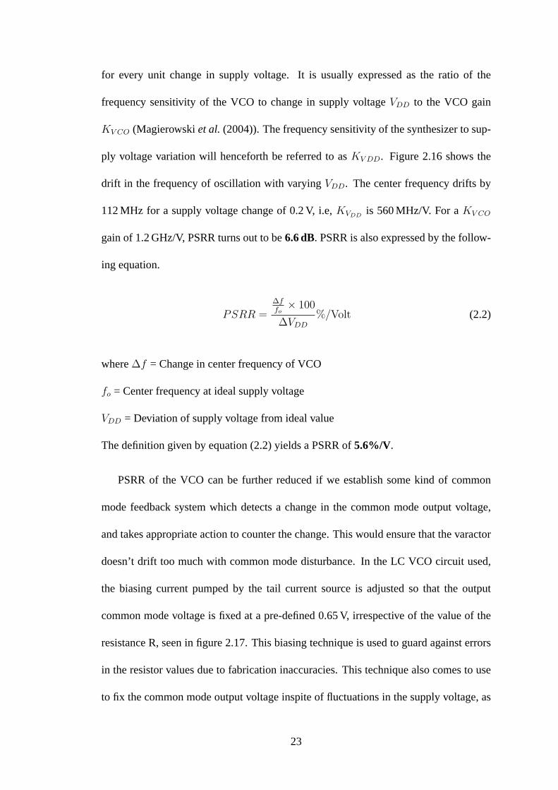
2.16 VCO’s frequency drift with change in supply voltage. . . . . . . . 24
2.17 Supply noise rejected by VCO with local biasing. . . . . . . . . . 25
2.18 VCO’s center frequency drift with change in supply (with local biasing)26
2.19 LC-VCO with pMOS current source. . . . . . . . . . . . . . . . . 27
2.20 Each DFF in the divider. . . . . . . . . . . . . . . . . . . . . . . . 28
2.21 Passive loop filter. . . . . . . . . . . . . . . . . . . . . . . . . . . 29
2.22 Loop gain before and after adding a zero. . . . . . . . . . . . . . . 31
2.23 Closed loop transfer function. . . . . . . . . . . . . . . . . . . . . 31
2.24 Control voltage of the simulated frequency synthesizer. . . . . . . 32
2.25 Control voltage upon giving a phase step ofπ/4 . . . . . . . . . . . 33

2.26 PLL of type I . . . . . . . . . . . . . . . . . . . . . . . . . . . . . 35
2.27 PLL of type II . . . . . . . . . . . . . . . . . . . . . . . . . . . . . 36
2.28 Lag-lead filter transfer function. . . . . . . . . . . . . . . . . . . . 37
2.29 PFD’s voltage response to input phase difference. . . . . . . . . . 37
2.30 PFD’s voltage response to input frequency difference. . . . . . . . 37
2.31 Noise contributed by various blocks. . . . . . . . . . . . . . . . . 39
2.32 Shaping of noise from various nodes to output. . . . . . . . . . . . 39
2.33 Gaussian jitter. . . . . . . . . . . . . . . . . . . . . . . . . . . . . 40
3.1 Receiver sampling the continuous-time data from the channel. . . . 43
3.2 Post and Pre Cursor ISI. . . . . . . . . . . . . . . . . . . . . . . . 44
3.3 ISI reduction by the FFE. . . . . . . . . . . . . . . . . . . . . . . 45
3.4 FFE block (Single-ended illustration). . . . . . . . . . . . . . . . 47
3.5 FFE circuit . . . . . . . . . . . . . . . . . . . . . . . . . . . . . . 48
3.6 Programmability of FFE co-efficients. . . . . . . . . . . . . . . . 49
3.7 Bode plot of the reflection co-efficient. . . . . . . . . . . . . . . . 49
3.8 Choosing the output conductance. . . . . . . . . . . . . . . . . . . 50
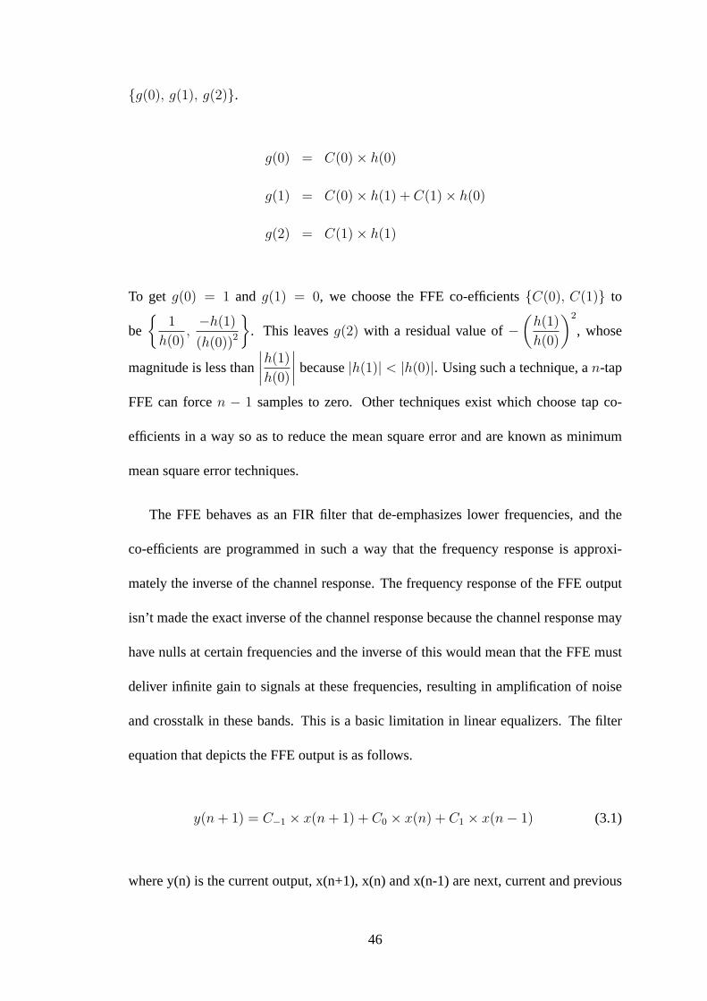
3.9 Illustrative plot of the reflection co-efficient. Dotted line shows themaximum allowableS22 . . . . . . . . . . . . . . . . . . . . . . . 51
3.10 Illustrative plot of input data and output of FFE with both pre and postcursor co-efficients activated. . . . . . . . . . . . . . . . . . . . . 53
3.11 Time domain understanding of post-cursor ISI removal. . . . . . . 54
3.12 Time domain understanding of pre-cursor ISI removal. . . . . . . . 54
3.13 Transmitter output waveform (IEEE 802.3ap(2007)) . . . . . . . . 56
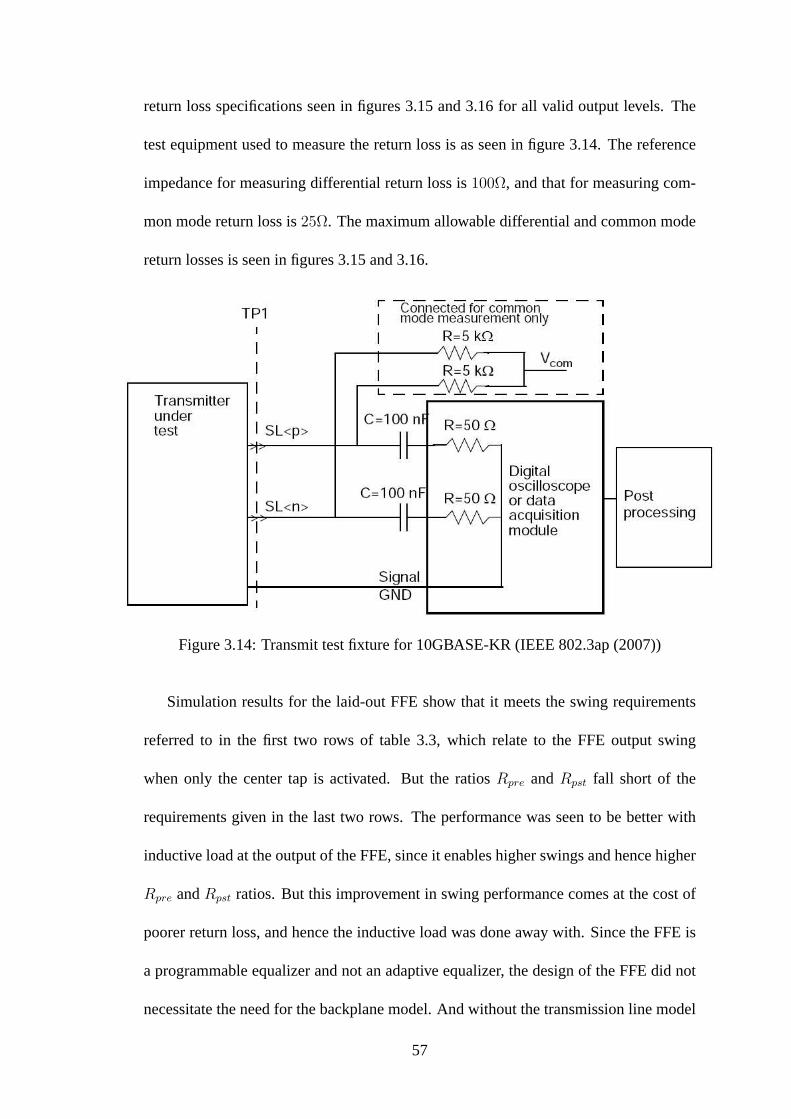
3.14 Transmit test fixture for 10GBASE-KR (IEEE 802.3ap(2007)) . . . 57
3.15 Maximum transmit differential output return loss (IEEE 802.3ap(2007)) 58
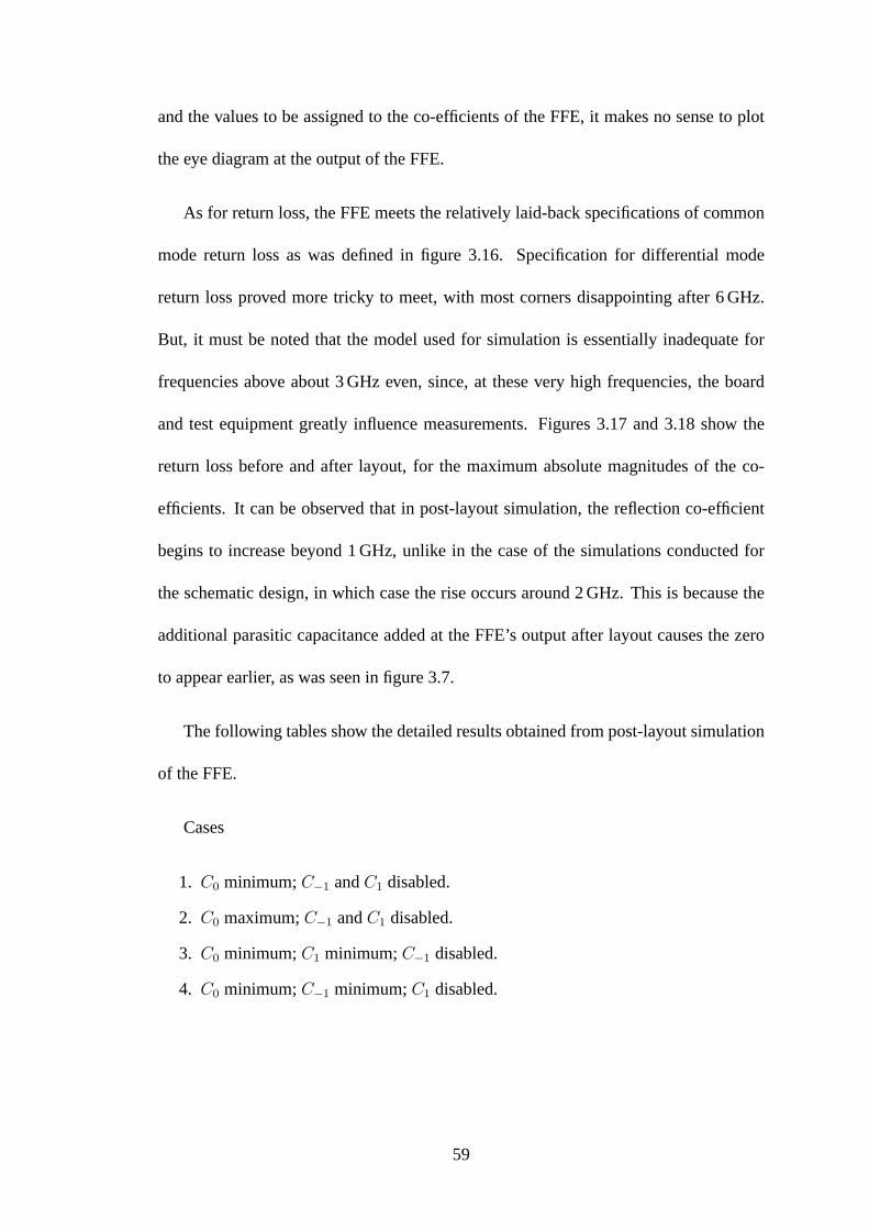
3.16 Maximum transmit common mode output return loss (IEEE 802.3ap(2007)) . . . . . . . . . . . . . . . . . . . . . . . . . . . . . . . . 58
3.17 Return loss over corners before layout. . . . . . . . . . . . . . . . 60
3.18 Return loss over corners post-layout. . . . . . . . . . . . . . . . . 61
3.19 Layout of the FFE. . . . . . . . . . . . . . . . . . . . . . . . . . . 62
4.1 4x1 MUX . . . . . . . . . . . . . . . . . . . . . . . . . . . . . . . 65
vii

4.2 2x1 CML MUX . . . . . . . . . . . . . . . . . . . . . . . . . . . . 66
4.3 2x1 CMOS MUX . . . . . . . . . . . . . . . . . . . . . . . . . . . 66
4.4 Layered architecture. . . . . . . . . . . . . . . . . . . . . . . . . 67
4.5 Illustration of select line generation. . . . . . . . . . . . . . . . . 67
5.1 Architecture of the clock/data recovery circuit. . . . . . . . . . . . 70
5.2 DLL architecture . . . . . . . . . . . . . . . . . . . . . . . . . . . 72
5.3 Simple phase detector used to lock the DLL. . . . . . . . . . . . . 72
5.4 DLL tracking behaviour . . . . . . . . . . . . . . . . . . . . . . . 73
5.5 Individual delay cell in the DLL . . . . . . . . . . . . . . . . . . . 74
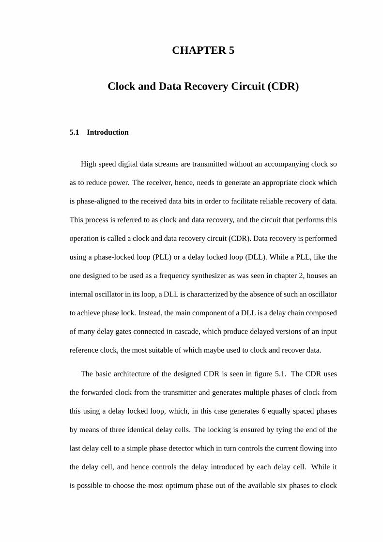
5.6 Delay cell with option to increase delay. . . . . . . . . . . . . . . 75
5.7 Latch used in the DLL phase detector’s D-flip flop. . . . . . . . . . 76
5.8 Circuits depicting operation of a phase interpolator. . . . . . . . . 78
5.9 Interpolator performance for input signals differing by60 . . . . . 79
5.10 Interpolator performance for input signals differing by150 . . . . . 80
5.11 Basic architecture of phase interpolator. . . . . . . . . . . . . . . 81
5.12 Circuit implementation of the interpolator with weight control at tailcurrent source. . . . . . . . . . . . . . . . . . . . . . . . . . . . . 82
5.13 Weight dependent delay at interpolator input. . . . . . . . . . . . . 85
5.14 Graphical explanation for non-monotonicity in phase interpolator. . 86
5.15 Design modification to remove weight dependent delay. . . . . . . 87
5.16 Performance of interpolator with tail current control. . . . . . . . . 88
5.17 Interpolator weight control at input nodes. . . . . . . . . . . . . . 89
5.18 Performance of interpolator with control at input nodes. . . . . . . 90
5.19 Interpolator non-monotonicity for4φ = 0.55 ps/unit increment in weight 91
5.20 Interpolator non-monotonicity for4φ = 1 ps/unit increment in weight 92
5.21 Architecture of the Alexander phase detector (Alexander(1975)) . . 93
5.22 3-point sampling of data by Alexander phase detector (Razavi(2002)) 94
5.23 Phase interpolator hunting noise. . . . . . . . . . . . . . . . . . . 95
6.1 Coupling in a transformer. . . . . . . . . . . . . . . . . . . . . . . 97
6.2 Symmetric differential inductor structure. . . . . . . . . . . . . . . 100
viii

6.3 Single ended inductor structure used differentially. . . . . . . . . . 101
6.4 Symmetric differential inductor model I (n=1, L=478 pH). . . . . . 102
6.5 Symmetric differential inductor model II (n=2, L=490 pH). . . . . 102
6.6 Symmetric differential inductor model III (n=3, L=475 pH). . . . . 103
6.7 Plot of mutual coupling to distance for symmetric inductor models. 103
6.8 Single ended inductor model I (n=1, L=600 pH). . . . . . . . . . . 105
6.9 Single ended inductor model II (n=1, L=550 pH). . . . . . . . . . 105
6.10 Single ended inductor model III (n=2.5, L=500 pH). . . . . . . . . 106
6.11 Inductor oriented at0 relative to the other. . . . . . . . . . . . . . 106
6.12 Inductor oriented at90 relative to the other. . . . . . . . . . . . . 107
6.13 Inductor stacked over the other. . . . . . . . . . . . . . . . . . . . 107
6.14 Plot of mutual coupling to distance for single ended inductor models108
6.15 Plot of mutual coupling to distance of single ended inductor model IIfor different orientations . . . . . . . . . . . . . . . . . . . . . . . 108
ix

CHAPTER 1
Introduction
A transceiver is a device that has both a transmitter and a receiver. 10GBASE-KR,
also known by its working group name 802.3ap, is a standard that defines signal trans-
mission over backplane ethernet at a bit rate of 10Gbps, used in applications such as
routers/switches. A backplane is a circuit board consisting of connectors made of con-
ductive paths or traces etched from copper sheets laminated onto a non-conductive
substrate. 10GBASE-KR implementations are required to operate in an environment
comprising up to 40 inches of copper printed circuit board with two connectors.
The basic building blocks of the transceiver we are designing are shown in figure
1.1. The transmitter consists of a frequency synthesizer that generates a 10 GHz clock
from a reference signal of 156.25 MHz produced by a crystal oscillator. The multiplexer
(MUX) serializes 32 channels, each of 312.5 Mbps, into a single data stream of 10 Gbps
using the frequency synthesizer’s output signal as its clock. The Feed-Forward Equal-
izer (FFE) is a 3-tap FIR filter whose tap co-efficients are programmed so that the FFE’s
frequency response is approximately the inverse of the channel’s frequency response,
in order to remove a part of the ISI that the channel would introduce when data passes
through it. The receiver consists of a 5-tap adaptive DFE (decision feedback equalizer)
preceded by a VGA (variable gain amplifier) to ensure a constant signal envelope at the
input of the DFE. The clock and data recovery circuit (CDR) uses the DFE’s output data
stream to extract the clock. The reclocked data is then demultiplexed into 32 channels
each of 312.5 Mbps.

32:1
MUX FFE
Frequency synthesizer
Channel
VGA
DFE 1:32
DEMUX
CDR
clk
clk
Transmitter
Receiver
Reference clk
312.5 Mbps
312.5 Mbps
Backplane
Figure 1.1:Block diagram of the transceiver
2

1.1 Motivation and Objectives
As the demand for higher data-rate communication increases, low-cost, high-speed
serial links using copper backplanes become attractive for short distances of upto 1
meter. Improvements in silicon technology continue to advance the clock rates of pro-
cessing cores and industry standards are being developed to define compliant channel
characteristics for operation at gigabit rates.
This work deals with the design of part of a 10Gbps transceiver consistent with
IEEE 802.3ap standard (10GBASE-KR), defined for gigabit ethernet copper backplane
transmission, which is the fastest among existing standards. At these speeds, the usual
problems encountered by any transceiver, like jitter-free clocking, channel distortion,
and reliable data recovery at the receiver, are aggravated. This work involves the design
of a frequency synthesizer which generates a 10GHz clock, a 3-tap programmable feed-
forward equalizer to counter channel distortion, and a clock/data recovery circuit (CDR)
to recover the received data. All of the design is undertaken in TSMC 65nm CMOS
process technology, which is among the latest commercially viable fabrication process
technologies in use.
1.2 Scope of the thesis
The thesis presents the design of all the blocks of the transmitter, namely the fre-
quency synthesizer, the multiplexer and the feed-forward equalizer. Of these, post-
layout simulation results of the feed-forward equalizer have been tabulated. Schematic
simulation results of the frequency synthesizer and the multiplexer have been presented
analyzed. Layout of the frequency synthesizer and multiplexer remain to be done at the
3

time of writing the thesis.
At the receiver end, the thesis discusses the analysis and design of the Clock and
Data Recovery (CDR) circuit. Discussion on the Variable Gain Amplifier (VGA), the
de-multiplexer and the Decision Feedback Equalizer (DFE) is beyond the scope of this
thesis.
1.3 Organization
The thesis is organized as follows. Chapters2, 3 and4 deal with the constituent
blocks of the transmitter, the blocks being a frequency synthesizer, a feed-forward
equalizer (FFE) and a multiplexer (MUX), respectively. Chapter5 deals with the design
of a DLL-based clock and data recovery circuit (CDR), which is part of the receiver.
Chapter6 is a study of a PLL-based CDR, with the PLL having a LC-VCO for its os-
cillator. This chapter deals with the coupling between the inductors of the CDR’s VCO
and the frequency synthesizer’s VCO, and suggests the architecture and orientation re-
quired off the inductors to keep coupling within tolerable limits. Chapter7 concludes
this thesis after stating the work that needs to be carried out in the future to bring out a
transceiver complying with IEEE 802.3ap.
4

CHAPTER 2
Frequency synthesizer
2.1 Introduction
A frequency synthesizer is an electronic device that generates a range of frequen-
cies from a stable frequency source like a crystal oscillator. Frequency synthesizers are
most commonly implemented using phase locked loops (PLLs) which function based
on the concept of negative feedback. The illustrative block diagram of the frequency
synthesizer is seen in figure2.1. A PLL compares the frequencies of two signals and
produces an error signal which is proportional to the difference between the input fre-
quencies. The error signal is then used to drive a voltage-controlled oscillator (VCO)
which pushes the output frequency in a direction which would reduce the error.
2.2 Phase/Frequency Detector (PFD)
The phase/frequency detector (PFD) is a circuit that produces an output proportional
to the difference in phase between the two signals that it sees at its input. The basic
architecture of the tristate PFD used in this design is seen in figure2.2. The D-flip flops
used for the current transceiver has been designed using true single phase clocked D-
Flip Flops as is shown in figure2.3. Plots2.4 to 2.7 show the functioning of the PFD
over different scenarios. Although the D-flip flops are implemented as dynamic logic,
the leakage current is of the order of only a few tens of nanoamps and not enough to

Pha
se/
Fre
quen
cyD
etec
tor
Cha
rge
Pum
pLo
opF
ilter
VC
O
Div
ider
Fre
quen
cy
Xta
lO
scill
ator
f ref
1/N
N.f r
ef
frequency synthesizer
(156
.25M
Hz)
(10G
Hz)
(1/6
4)
Figure 2.1:Block diagram of a frequency synthesizer
6

cause any significant change in the output voltage within the duration of one reference
clock period.
From the simulated plots of the PFD, we notice that, if the frequencies of the input
signals are equal, then the average value ofUP − DN is proportional to the phase
difference between the two signals. But if one of the signals has a higher frequency
than the other, then at the UP (or DN) node, we get pulses with varying width repeating
with a frequency equal to the difference in the frequencies off1 andf2; while the DN
(or UP) node is almost zero.
Another interesting feature is the small but finite width pulses that appear even if
the two signals are perfectly in phase. This is due to finite delay in the reset path, i.e,
the time it takes for the flip flop to get reset to logic low after the reset signal has been
triggered. This can reduce the linear range of a PFD as shown in figure2.8 (Mansuri
et al. (2002)). Here,Vout is the average or DC value of the voltage output(up− dn) of
the PFD. In the figure2.84φ =2π
Tτ , whereτ is the reset delay. But this reduction in
linear range is very small in the designed PFD. The reset delay is about 30 ps, which is
less than 0.5 % of a time period of the reference signal.
While the PFD, being a CMOS implemented circuit, doesn’t use up any static power,
it burns a dynamic power of not more than 35µW.
2.3 Charge Pump
The charge pump is a circuit that either drives in a constant current into, or sinks an
identical amount of current from the loop filter, depending on the input received from
the phase detector preceding it. Such a current source driving constant current into a
7

D
D
clk
clk
up
dn
Rst
Rst
Vdd
A
B
Q
Q
Figure 2.2:Block diagram of the PFD
Vdd
clk
Rst
Q
Mp1 Mp2
Mp3
Mn2 Mn3
Mn1
Mp: (8)x450n/60n
Mn: (4)x300n/60n
Figure 2.3:Circuit diagram of each TSPC flip-flop in the PFD (Leeet al. (1999))
8

Figure 2.4:PFD:Two signals of same frequency, butf1 leads in phase
9

Figure 2.5:PFD:Two signals of same frequency, butf2 leads in phase
10

Figure 2.6:PFD:Two signals of same frequency and in phase with each other
11

Figure 2.7:PFD:Signalf1 is of greater frequency thanf2
Avg. Vout
2π φ4π
-2π-4π
No reset delay
Avg. Vout
φ
-4π -2π
2π 4π
∆φ
Non-zero reset delay
PFD characteristic
Figure 2.8:PFD non-ideality due to reset delay
12
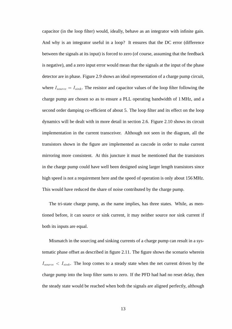
capacitor (in the loop filter) would, ideally, behave as an integrator with infinite gain.
And why is an integrator useful in a loop? It ensures that the DC error (difference
between the signals at its input) is forced to zero (of course, assuming that the feedback
is negative), and a zero input error would mean that the signals at the input of the phase
detector are in phase. Figure2.9shows an ideal representation of a charge pump circuit,
whereIsource = Isink. The resistor and capacitor values of the loop filter following the
charge pump are chosen so as to ensure a PLL operating bandwidth of 1 MHz, and a
second order damping co-efficient of about 5. The loop filter and its effect on the loop
dynamics will be dealt with in more detail in section2.6. Figure2.10shows its circuit
implementation in the current transceiver. Although not seen in the diagram, all the
transistors shown in the figure are implemented as cascode in order to make current
mirroring more consistent. At this juncture it must be mentioned that the transistors
in the charge pump could have well been designed using larger length transistors since
high speed is not a requirement here and the speed of operation is only about 156 MHz.
This would have reduced the share of noise contributed by the charge pump.
The tri-state charge pump, as the name implies, has three states. While, as men-
tioned before, it can source or sink current, it may neither source nor sink current if
both its inputs are equal.
Mismatch in the sourcing and sinking currents of a charge pump can result in a sys-
tematic phase offset as described in figure2.11. The figure shows the scenario wherein
Isource < Isink. The loop comes to a steady state when the net current driven by the
charge pump into the loop filter sums to zero. If the PFD had had no reset delay, then
the steady state would be reached when both the signals are aligned perfectly, although
13

Vdd
up
dn
Isource
Isink
R1
C1
C2
Vctrl
Iout
Loop FilterCharge Pump
Isource = Isink = 20µA
R=16.7kΩ
C1=950pF
C2=670fF
Figure 2.9:Ideal representation of a charge pump
14

Vdd Vdd
Vdd
up
dn
Icp
Iout
Mn1 Mn1
Mp1 Mp1 Mp2
Mn2
Mp3
Mn3
Icp=80µA
Iout=20µA
Mp1,Mp2=(8)x720n/60n
Mn1=(4)x240n/60n
Mp3=(2)x720n/60n
Mn2=(8)x240n/60n
Mn3=(2)x240n/60n
Figure 2.10:Circuit implementation of charge pump
15

τt
up
dn
Isource
Isink
Figure 2.11:Current mismatch in a charge pump (here,Isource < Isink)
16

the mismatch in charge pump currents would result in a different rate of lock acquisi-
tion when the PLL needs to catch up with a higher reference frequency than for the case
when the PLL needs to slow down to match the reference frequency.
If we bring into consideration the finite reset delay of the PFD, referred to asτ ,
which results in narrow pulses with widths equalling the delay time, then at steady
state, the total charge transferred to the loop filter must be zero, i.e, the area of the
current curves in figure2.11 must be equal. We can hence compute the finite phase
offset ’t’ as follows
Isource × (t+ τ) = Isink × τ
⇒ t =
(Isink
Isource
− 1
)τ
⇒ φ =2π
Tτ
(Isink
Isource
− 1
)(2.1)
where T is the time period of the reference signal.
For the circuit designed, the reset delay is about 30 ps, which translates to a phase
offset of less than0.2 for a current mismatch of 10%. The current mismatch in a charge
pump is influenced, among others, by the output node voltage, in this case the control
voltage of the VCO. Too small or too large a control voltage can lead to significant
current mismatch. Hence, it is necessary to keep the output node voltage within a safe
range. Simulation results show that in this circuit, the voltage range turns out to be
between 0.2 V and 0.8 V in order to limit the mismatch to less than 10%.
The charge pump dissipates a power of about100µW.
17
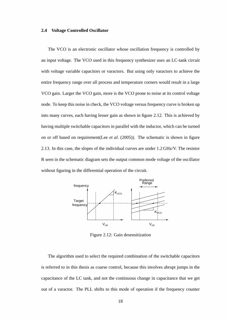
2.4 Voltage Controlled Oscillator
The VCO is an electronic oscillator whose oscillation frequency is controlled by
an input voltage. The VCO used in this frequency synthesizer uses an LC-tank circuit
with voltage variable capacitors or varactors. But using only varactors to achieve the
entire frequency range over all process and temperature corners would result in a large
VCO gain. Larger the VCO gain, more is the VCO prone to noise at its control voltage
node. To keep this noise in check, the VCO voltage versus frequency curve is broken up
into many curves, each having lesser gain as shown in figure2.12. This is achieved by
having multiple switchable capacitors in parallel with the inductor, which can be turned
on or off based on requirement(Lee et al. (2005)). The schematic is shown in figure
2.13. In this case, the slopes of the individual curves are under 1.2 GHz/V. The resistor
R seen in the schematic diagram sets the output common mode voltage of the oscillator
without figuring in the differential operation of the circuit.
KVCO
Vctrl Vctrl
frequency
Targetfrequency
KVCO
PreferredRange
Figure 2.12:Gain desensitization
The algorithm used to select the required combination of the switchable capacitors
is referred to in this thesis as coarse control, because this involves abrupt jumps in the
capacitance of the LC tank, and not the continuous change in capacitance that we get
out of a varactor. The PLL shifts to this mode of operation if the frequency counter
18

Vdd
Vctrl
R
L
Cvar Cvar
C32
C1C1
C32
Digital coarsecontrol
Itail
M1 M1
Itail=4.3mA
M1=(40)x960n/60n
R=120Ω
L=540pH
C1...32=50fF
Cvar=140fF-240fF
Switch (nMOS) switch
(20)x2.4u/60n
Figure 2.13:Schematic of the LC-VCO
19

detects that the PLL has lost lock. The algorithm used to switch between the capacitors
in the oscillator can be broadly classified into two different strategies. One method in-
volves monitoring the control voltage of the VCO. If the control voltage strays beyond
a pre-defined voltage range, capacitors are introduced or discarded. In the second algo-
rithm, an external frequency counter is used to detect the frequency difference between
the reference signal and the signal at the divider output. If the difference breaches a
pre-defined value, capacitors are shunted in or out. The circuit oscillates even with the
parasitic resistance offered by the nMOS switches. In this work, we use a frequency
counter, as mentioned, to check if the PLL is in lock, since a digital frequency counter
makes for an easier design than a multi-level comparator. The frequency counter used
for this design was a behavioral model of a digital block that keeps track of the differ-
ence in the number of positive edges between the two signals whose frequencies need
to be compared.
In the designed VCO, the PLL moves into coarse control mode if it detects that the
frequency is off by over 0.5 GHz. Since the beat frequency is measured after the divider,
this would mean that the frequency comparator switches to coarse control if the divider
is off by 7.8 MHz from the reference frequency. Once in this mode, the control voltage
of the VCO is set to 0.5 V and the capacitors are chosen so as to bring the frequency
between 9.75 GHz and 10.25 GHz before handing the control back to the conventional
(fine control) loop. This idea is illustrated in figure2.14.
The VCO yields a worst-scenario phase noise performance of about -90 dBc/Hz at
1 MHz offset from the carrier frequency of 10 GHz, the largest contributors of the noise
being the tail current transistor and its current mirror pair, each of which account for
20
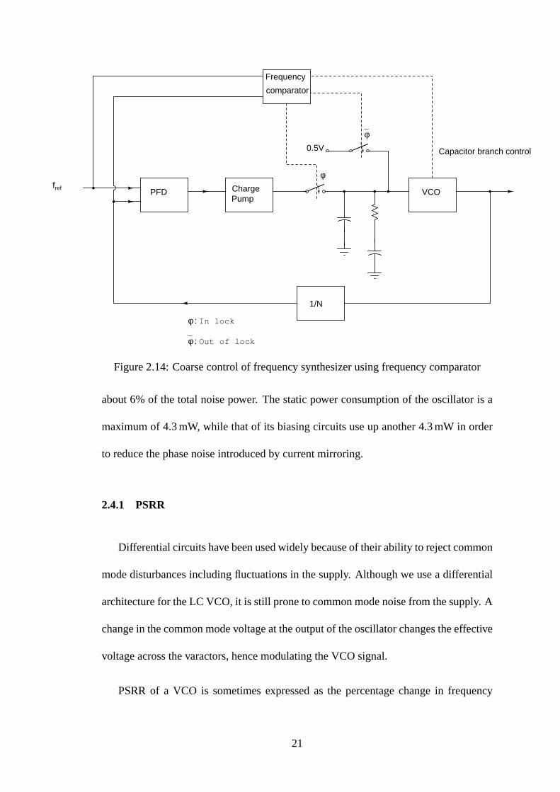
PFD ChargePump
0.5V
VCO
1/N
fref
Frequency
comparator
Capacitor branch control
φ
φ
φ : In lock
φ : Out of lock
Figure 2.14:Coarse control of frequency synthesizer using frequency comparator
about 6% of the total noise power. The static power consumption of the oscillator is a
maximum of 4.3 mW, while that of its biasing circuits use up another 4.3 mW in order
to reduce the phase noise introduced by current mirroring.
2.4.1 PSRR
Differential circuits have been used widely because of their ability to reject common
mode disturbances including fluctuations in the supply. Although we use a differential
architecture for the LC VCO, it is still prone to common mode noise from the supply. A
change in the common mode voltage at the output of the oscillator changes the effective
voltage across the varactors, hence modulating the VCO signal.
PSRR of a VCO is sometimes expressed as the percentage change in frequency
21
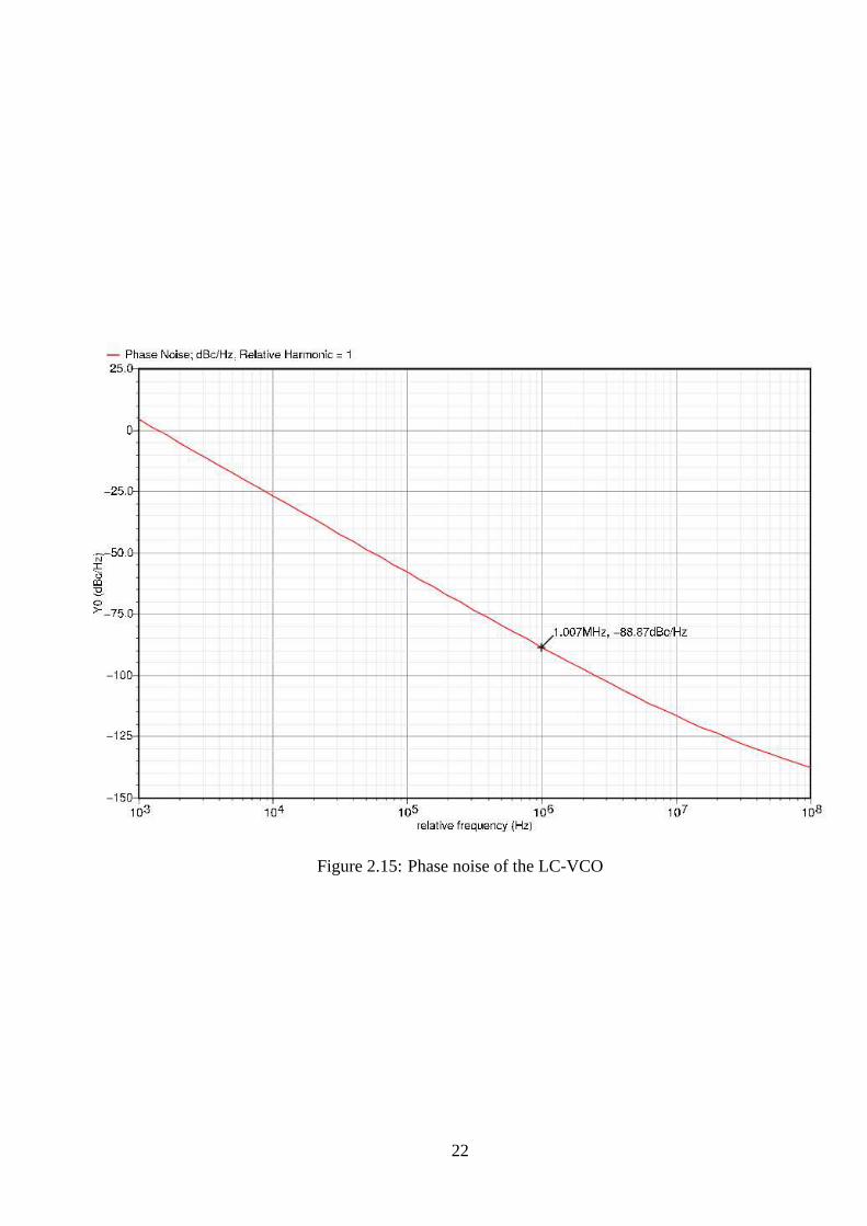
Figure 2.15:Phase noise of the LC-VCO
22
for every unit change in supply voltage. It is usually expressed as the ratio of the
frequency sensitivity of the VCO to change in supply voltageVDD to the VCO gain
KV CO (Magierowskiet al.(2004)). The frequency sensitivity of the synthesizer to sup-
ply voltage variation will henceforth be referred to asKV DD. Figure2.16shows the
drift in the frequency of oscillation with varyingVDD. The center frequency drifts by
112 MHz for a supply voltage change of 0.2 V, i.e,KVDDis 560 MHz/V. For aKV CO
gain of 1.2 GHz/V, PSRR turns out to be6.6 dB. PSRR is also expressed by the follow-
ing equation.
PSRR =
∆ffo× 100
∆VDD
%/Volt (2.2)
where∆f = Change in center frequency of VCO
fo = Center frequency at ideal supply voltage
VDD = Deviation of supply voltage from ideal value
The definition given by equation (2.2) yields a PSRR of5.6%/V.
PSRR of the VCO can be further reduced if we establish some kind of common
mode feedback system which detects a change in the common mode output voltage,
and takes appropriate action to counter the change. This would ensure that the varactor
doesn’t drift too much with common mode disturbance. In the LC VCO circuit used,
the biasing current pumped by the tail current source is adjusted so that the output
common mode voltage is fixed at a pre-defined 0.65 V, irrespective of the value of the
resistance R, seen in figure2.17. This biasing technique is used to guard against errors
in the resistor values due to fabrication inaccuracies. This technique also comes to use
to fix the common mode output voltage inspite of fluctuations in the supply voltage, as
23
0.9 0.95 1 1.05 1.110
10.05
10.1
10.15
VDD
Cen
ter
freq
uenc
y
Figure 2.16:VCO’s frequency drift with change in supply voltage
is shown in figure2.17. But such a local biasing The gate potential generated by the
amplifier is such that the current through the resistor is enough to ensure thatVD,o =
Vcm,o even with a varyingVDD. Usually this kind of biasing circuitry is placed far away
from other designs, and only the biasing currents are routed to various parts of the chip
where they are mirrored and multiplied in quantity in order to power other circuits.
But the supply variation in one part of the chip may well differ from the variation in
another part, and so the generated bias currents may not be sufficient to account for the
changes in supply near the design of interest. But if we can have a local biasing circuitry
placed very close to this design, in our case, the LC VCO, then the supply variations
affecting the biasing circuit will resemble that felt by the VCO, and the generated bias
current effectively cancels the impact of supply disturbance on the output voltage, hence
reducing the influence ofVDD on the varactor’s capacitance. The center frequency drifts
by 12 MHz for a supply voltage drift of 0.2 V. To compare the sensitivity of the VCO to
power supply and control voltage,KVDDis 60 MHz/V, which is
1
20th of the VCO gain
24

(KV CO) of 1.2 GHz/V. PSRR comes to be about26 dB, or0.6%/V. This is about 9 times
the rejection obtained when the tail current is not biased in a way that keeps the output
common mode voltage constant. The definition of PSRR used in this thesis quantifies
supply rejection at DC. But in this technology the bandwidth of the local biasing circuit
extends to a few gigahertz and hence can be taken as a good measure for power supply
rejection. Figure2.18shows the drift in the oscillation frequency with change inVDD.
The sharp breaks in the plot is due to linear interpolation between a finite number of
points.
Vdd
Vctrl
R
L
Cvar Cvar
C C
R
+
-Vcm,o
Vcm,oVcm,o
(W/L)0
Biasing circuit
(W/L)0
(W/L)1
2(W/L)1
Figure 2.17:Supply noise rejected by VCO with local biasing
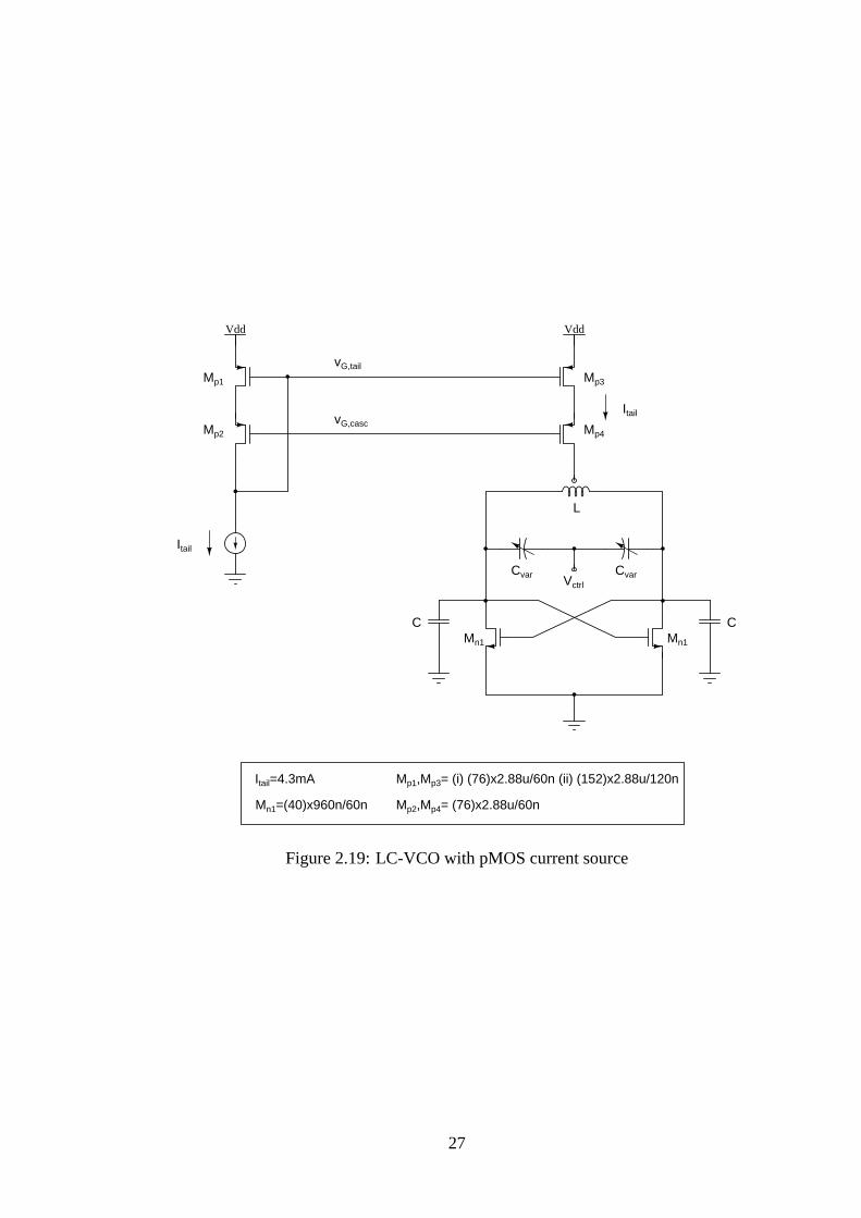
A second, slightly different architecture of an LC VCO was also tested for PSRR.
The architecture is seen in figure2.19. This architecture was chosen for comparison
because it has an inherent ability to reject supply noise. This is so because the gate of
25
0.9 0.95 1 1.05 1.1 1.1510.07
10.072
10.074
10.076
10.078
10.08
10.082
10.084
VDD
Cen
ter
freq
uenc
y
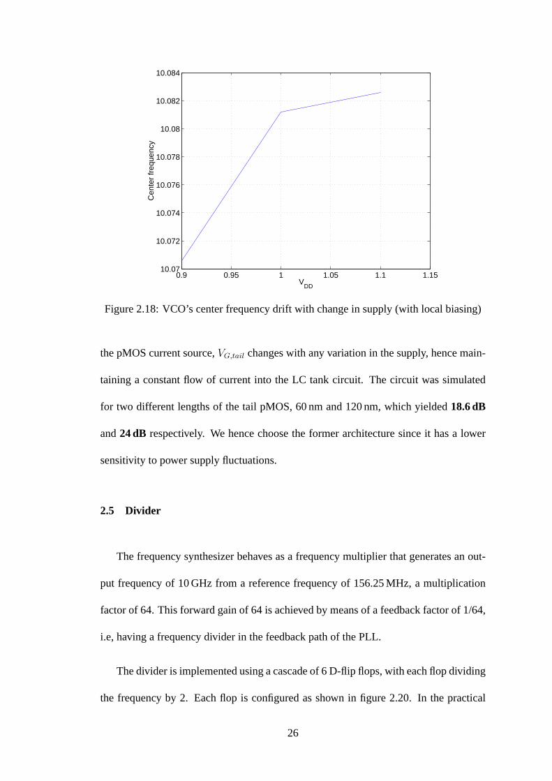
Figure 2.18:VCO’s center frequency drift with change in supply (with local biasing)
the pMOS current source,VG,tail changes with any variation in the supply, hence main-
taining a constant flow of current into the LC tank circuit. The circuit was simulated
for two different lengths of the tail pMOS, 60 nm and 120 nm, which yielded18.6 dB
and24 dB respectively. We hence choose the former architecture since it has a lower
sensitivity to power supply fluctuations.
2.5 Divider
The frequency synthesizer behaves as a frequency multiplier that generates an out-
put frequency of 10 GHz from a reference frequency of 156.25 MHz, a multiplication
factor of 64. This forward gain of 64 is achieved by means of a feedback factor of 1/64,
i.e, having a frequency divider in the feedback path of the PLL.
The divider is implemented using a cascade of 6 D-flip flops, with each flop dividing
the frequency by 2. Each flop is configured as shown in figure2.20. In the practical
26
Vctrl
L
Cvar Cvar
C C
VddVdd
Itail
vG,tail
vG,casc
Itail
Mn1 Mn1
Mp1
Mp2
Mp3
Mp4
Itail=4.3mA
Mn1=(40)x960n/60n
Mp1,Mp3= (i) (76)x2.88u/60n (ii) (152)x2.88u/120n
Mp2,Mp4= (76)x2.88u/60n
Figure 2.19:LC-VCO with pMOS current source
27
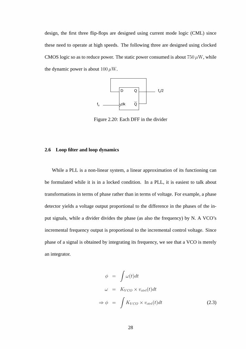
design, the first three flip-flops are designed using current mode logic (CML) since
these need to operate at high speeds. The following three are designed using clocked
CMOS logic so as to reduce power. The static power consumed is about750µW, while
the dynamic power is about100µW.
D
clk
Q
Qfo
fo/2
Figure 2.20:Each DFF in the divider
2.6 Loop filter and loop dynamics
While a PLL is a non-linear system, a linear approximation of its functioning can
be formulated while it is in a locked condition. In a PLL, it is easiest to talk about
transformations in terms of phase rather than in terms of voltage. For example, a phase
detector yields a voltage output proportional to the difference in the phases of the in-
put signals, while a divider divides the phase (as also the frequency) by N. A VCO’s
incremental frequency output is proportional to the incremental control voltage. Since
phase of a signal is obtained by integrating its frequency, we see that a VCO is merely
an integrator.
φ =
∫ω(t)dt
ω = KV CO × vctrl(t)dt
⇒ φ =
∫KV CO × vctrl(t)dt (2.3)
28
The most basic form of a loop filter is a capacitor at the output of the charge pump. This
would mean that the combination of the PFD, charge pump and the filter behaves as an
integrator, in addition to the integrator in the form of a VCO. Here, though, we assume
that the charge pump’s output current is proportional to the phase difference, although
the design specifies only three states for the charge pump (−20µA, 0 A, +20µA). But
this linearization holds fairly accurately since the average current over a period of time
turns out to be proportional to the phase difference, provided the loop bandwidth be
much smaller than the reference frequency.
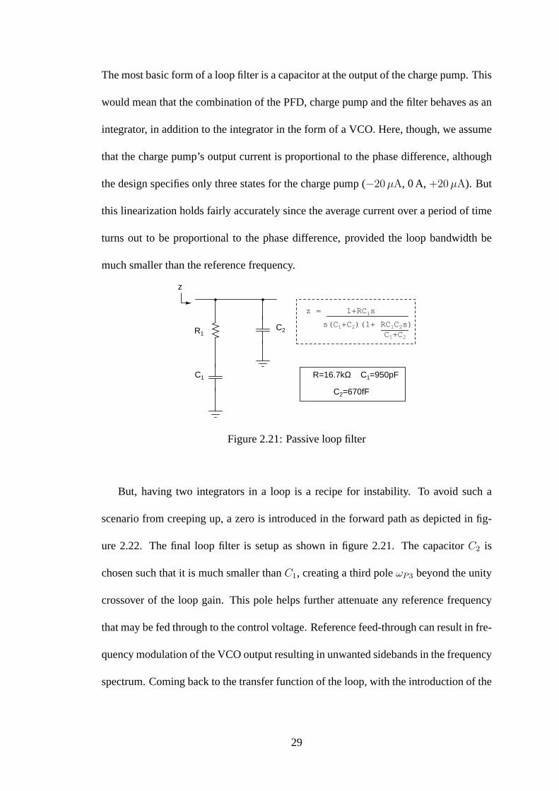
R1
C1
C2
R=16.7kΩ C1=950pF
C2=670fF
z = 1+RC1s
s(C1+C2)(1+ RC1C2s)
z
C1+C2
Figure 2.21:Passive loop filter
But, having two integrators in a loop is a recipe for instability. To avoid such a
scenario from creeping up, a zero is introduced in the forward path as depicted in fig-
ure 2.22. The final loop filter is setup as shown in figure2.21. The capacitorC2 is
chosen such that it is much smaller thanC1, creating a third poleωP3 beyond the unity
crossover of the loop gain. This pole helps further attenuate any reference frequency
that may be fed through to the control voltage. Reference feed-through can result in fre-
quency modulation of the VCO output resulting in unwanted sidebands in the frequency
spectrum. Coming back to the transfer function of the loop, with the introduction of the
29

zero (due to resistorR1), the loop gain is as follows
I.KV CO
2πNCs2(1 + sR1C1) (2.4)
The unit ofKV CO is rad/s/V. The closed loop gain is
φout
φin
=
I.KV CO
2πC1
(1 + sR1C1)
s2 +IR1KV CO
2πNs+
I.KV CO
2πNC
(2.5)
The damping factor and natural frequency of the loop is as given below
ζ =R1
2
√IC1KV CO
2πN(2.6)
ωn =
√IKV CO
2πNC1
(2.7)
For a large damping factor (in our case, about 5), the following are the closed loop
parameters, all units being rad/s.
ωz =ωn
2ζ=
1
R1C1
(2.8)
ωP1 ≈ ωz =1
R1C1
(2.9)
ωBW = ωP2 = 2ζωn =IR1KV CO
2πN(2.10)
Figure2.24shows the control voltage of the simulated frequency synthesizer. Phase
step was also provided at the reference input, and the corresponding control voltage
response is shown magnified in figure2.25.
We notice the phase step as a spike in the control voltage due to an abrupt, dis-
30

40 dB/dec
ωn
Bode Plot of loop gain
ωz
ωBW ωp3
40 dB/dec
40 dB/dec
20 dB/dec
Mag
Phase
-180 deg
-90 deg
-180 deg
Mag
Phase
Figure 2.22:Loop gain before and after adding a zero
Bode plot of closed loop transfer function
ωz ωp1 ωBW
N
Mag
20 dB/dec
Figure 2.23:Closed loop transfer function
31

Figure 2.24:Control voltage of the simulated frequency synthesizer
32
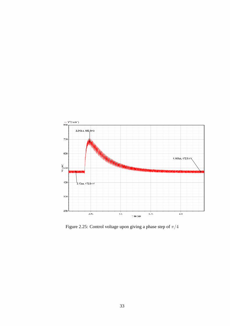
Figure 2.25:Control voltage upon giving a phase step ofπ/4
33
continuous change in the phase of the signal. This can be thought of as an impulse
response of the loop to an input frequency impulse. The phase step and frequency step
response can be used to verify the gain of the VCO at the operating point. The area
under the control voltage curve upon giving a phase step at the reference input follows
the equation below.
4 φ =1
N
∫KV CO.vctrl(t)dt (2.11)
This equation reveals that the VCO gain at the operating point is about 1.2 GHz/V.
Calculating the VCO gain from a frequency step response is more straight forward, and
this gives a gain of 1.1 GHz/V. These results match with the simulation results of an
isolated LC-VCO block.
2.6.1 Hold and Lock ranges
Hold range of a PLL is the maximum frequency step which it can lock onto eventu-
ally, whereas, lock range of a PLL is the maximum frequency offset between the inputs
of the phase detector, for which lock is acquired without cycle slipping, i.e, within a
single beat note. The lock range is always less than or equal to the hold range, the two
being equal for a first order loop. The terminology is derived from the book byEgan
(1981).
PLLs are classified depending on the number of integrators in the loop, a type I
PLL having just the one integrator, which is the VCO, in its loop. A charge pump
PLL, like the frequency synthesizer designed in this work, is a type II PLL. The order
of a PLL is the number of poles in its loop gain. A PLL has atleast as many poles as
34

its type, with extra poles added by non-integrating filters in the loop. The frequency
synthesizer designed is of type II and order 3. To define the hold and lock range of
our PLL, let us first start from a type I PLL, shown in figure2.26. The loop gain of
this system isKPDKV CO
Ns, whereKPD is V/rad andKV CO is in rad/s/V. The VCO of
a PLL has a free running frequency, which is the frequency of oscillation when the
control voltage is zero. If a PLL were to track a reference frequency that is not equal
to the free running frequency of the VCO (which is almost always the case), the VCO
needs a steady control voltage at its input. In a first order PLL, this control voltage
can only be maintained if there exists a non-zero phase difference at the input to the
phase detector, the larger the difference in frequency, larger the phase offset required
to maintain frequency lock. In essence, a first order PLL can lock to the reference
frequency but not phase, and the range of frequencies which the PLL can track is limited
by the fact that the offset in the input phase cannot exceed2π. The maximum frequency
that such a PLL can track, which is the frequency attained when the phase detector sees
an offset of2π at its input, isωH =2πKPDKV CO
Nrad/s. This is also the lock range of
the PLL because, as long as the step in the reference frequency is less than this range,
the control voltage responds immediately to the step and establishes lock without delay.
φref
1/N
KPD
KVCO
sΣ
+
-
φout
φfb
Figure 2.26:PLL of type I
35
1/N
KPD
KVCO
s
KPD,I
Σ+
+
s
Σφref
φfb
φout+
-
Figure 2.27:PLL of type II
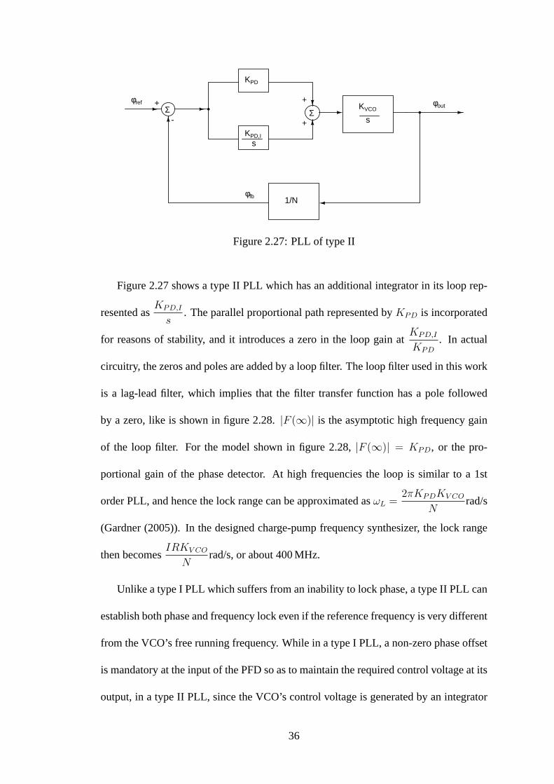
Figure2.27shows a type II PLL which has an additional integrator in its loop rep-
resented asKPD,I
s. The parallel proportional path represented byKPD is incorporated
for reasons of stability, and it introduces a zero in the loop gain atKPD,I
KPD
. In actual
circuitry, the zeros and poles are added by a loop filter. The loop filter used in this work
is a lag-lead filter, which implies that the filter transfer function has a pole followed
by a zero, like is shown in figure2.28. |F (∞)| is the asymptotic high frequency gain
of the loop filter. For the model shown in figure2.28, |F (∞)| = KPD, or the pro-
portional gain of the phase detector. At high frequencies the loop is similar to a 1st
order PLL, and hence the lock range can be approximated asωL =2πKPDKV CO
Nrad/s
(Gardner(2005)). In the designed charge-pump frequency synthesizer, the lock range
then becomesIRKV CO
Nrad/s, or about 400 MHz.
Unlike a type I PLL which suffers from an inability to lock phase, a type II PLL can
establish both phase and frequency lock even if the reference frequency is very different
from the VCO’s free running frequency. While in a type I PLL, a non-zero phase offset
is mandatory at the input of the PFD so as to maintain the required control voltage at its
output, in a type II PLL, since the VCO’s control voltage is generated by an integrator
36

|F(∞)|
ωz ω
|H(ω)|
Figure 2.28:Lag-lead filter transfer function
iout
2π φ4π-2π-4π
i
-i
Figure 2.29:PFD’s voltage response to input phase difference
iout
i/2
-i/2
fref-fdiv<0
0 fref-fdiv>0
Figure 2.30:PFD’s voltage response to input frequency difference
37
(charge pump cascaded with loop filter), we can dispense with the non-zero phase offset
at the PFD’s input, enabling the PLL to lock to the phase of the reference frequency as
well.
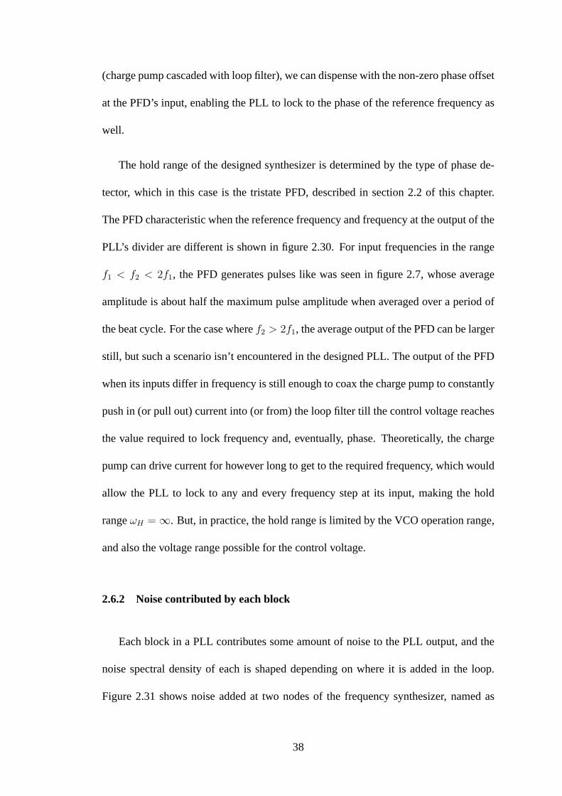
The hold range of the designed synthesizer is determined by the type of phase de-
tector, which in this case is the tristate PFD, described in section2.2 of this chapter.
The PFD characteristic when the reference frequency and frequency at the output of the
PLL’s divider are different is shown in figure2.30. For input frequencies in the range
f1 < f2 < 2f1, the PFD generates pulses like was seen in figure2.7, whose average
amplitude is about half the maximum pulse amplitude when averaged over a period of
the beat cycle. For the case wheref2 > 2f1, the average output of the PFD can be larger
still, but such a scenario isn’t encountered in the designed PLL. The output of the PFD
when its inputs differ in frequency is still enough to coax the charge pump to constantly
push in (or pull out) current into (or from) the loop filter till the control voltage reaches
the value required to lock frequency and, eventually, phase. Theoretically, the charge
pump can drive current for however long to get to the required frequency, which would
allow the PLL to lock to any and every frequency step at its input, making the hold
rangeωH = ∞. But, in practice, the hold range is limited by the VCO operation range,
and also the voltage range possible for the control voltage.
2.6.2 Noise contributed by each block
Each block in a PLL contributes some amount of noise to the PLL output, and the
noise spectral density of each is shaped depending on where it is added in the loop.
Figure2.31 shows noise added at two nodes of the frequency synthesizer, named as
38

PFD + CP VCO
Divider
φn,ref
φn,div
Σ
Σ
R1
φn,VCO
in,CP
C1
Node 1
Node 2
Σ
φn,CP
OutputNode
Figure 2.31:Noise contributed by various blocks
N|HLPF(ω)|
ωz
ωBW
|HHPF(ω)|
-20dB/dec
20dB/dec
40dB/dec
Node1 to output
Node2 to output
1
Figure 2.32:Shaping of noise from various nodes to output
39
T
5.68σ
10Gbps data
10GHz clock
T/2
Gaussian distributionaround clock edge
Figure 2.33:Gaussian jitter
nodes 1 and 2. The transfer functions from the two nodes to the synthesizer output are
low pass and high pass respectively, as seen in figure2.32. The equivalent jitter variance
at the output is given by the following equations
φ2n,total(f) =
(φ2
n,div(f) + φ2n,CP (f)
) |HLPF (f)|2 + φ2n,V CO|HHPF (f)|2
σ24t =
2
ω2σ24φ =
2
ω2
∫ ∞
fcenter
φ2n,total(f)df (2.12)
The multiplying factor of 2 in the above equation takes into account phase noise due to
both the side-bands. The frequency synthesizer is to be designed to achieve a BER <
10−15. The rms jitter specification is obtained by assuming a Gaussian distribution of
random jitter as shown in figure2.33. The area under the Gaussian distribution curve
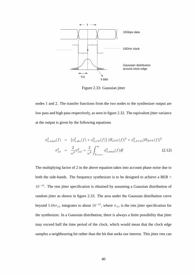
beyond5.68σ4t integrates to about10−15, whereσ4t is the rms jitter specification for
the synthesizer. In a Gaussian distribution, there is always a finite possibility that jitter
may exceed half the time period of the clock, which would mean that the clock edge
samples a neighbouring bit rather than the bit that seeks our interest. This jitter rms can
40
be quantified as follows.
5.68σ4t =T
2= 50 p
⇒ σ4t = 8.8 ps (2.13)
This is the BER required at the receiver end, and it places a much more stringent jitter
requirement for the transmitter. The frequency synthesizer is designed to meet jitter
specification of less than 1 ps rms.
41

CHAPTER 3
Feed-Forward Equalizer
3.1 Introduction
Channel equalization is the process of reducing amplitude, frequency and phase dis-
tortion in a channel with the intent of improving transmission performance. The FFE
is a linear equalizer which pre-distorts the signal such that it becomes easier for the re-
ceiver to recover the signal reliably. Since the channel essentially behaves as a low pass
filter, the FFE is implemented as a low frequency de-emphasis process which reduces
the low frequency signal components in proportion to the attenuation experienced by the
high frequency components of the signal, hence ensuring that the receiver sees a con-
stant envelope of the incoming datastream (Bulzacchelliet al. (2006)). The following
sections of this chapter delve more into the theory behind equalization, and the details
of circuit design that goes behind its practical implementation. The chapter ends with
a reference to the specifications that the FFE needs to meet as part of 10GBASE-KR
standards.
3.2 Theory behind Equalization
3.2.1 Inter-Symbol Interference (ISI)
ISI is a form of distortion of a signal which causes a transmitted symbol to have
an effect on the symbols transmitted before and after it. The channel over which rect-
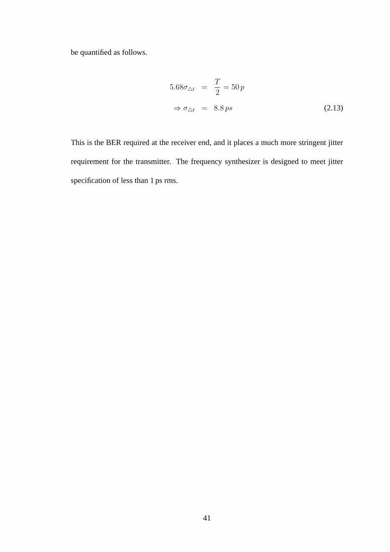
angular data waveform is transmitted has a continuous time impulse response, and the
Channel
TS
TS
Discrete-time Continuous-timepulse
Continuous-time
data pulse shaping
Smearedcontinuous-time
pulse Data with ISI
Transmitter
Receiver
Figure 3.1:Receiver sampling the continuous-time data from the channel
43

resulting signal is sampled at the receiver, as seen in figure3.1. In figure3.2is seen the
impulse response of a fictional low-pass channel. When an impulse, whose frequency
spectrum extends to infinity, is fed to a band-limited system, the response is a smeared
signal that now has a skirt around it with finite rise and fall times. The smearing occurs
because of the suppression of higher frequencies in the signal due to the finite band-
width of the system, and the resulting vestige extends into the previous and subsequent
symbols. The effect it has on previously transmitted signals is called pre-cursor ISI,
and the effect on the subsequently transmitted signals is called post-cursor ISI (Figure
3.2). If the impulse response of the channel is known, we can remove ISI by using a
filter that does to the signal exactly the opposite of what the band-limited system did to
it. In our case, the band-limited system is the channel connecting the transmitter to the
receiver, and the filter used is called Feed Forward Equalizer (FFE).
Pre-cursor ISI Post-cursor ISI
nT
nT0 1 2-1
Sampling instants
Input toband limited system
Impulse response
1
1
3
0.50.30.1
Figure 3.2:Post and Pre Cursor ISI
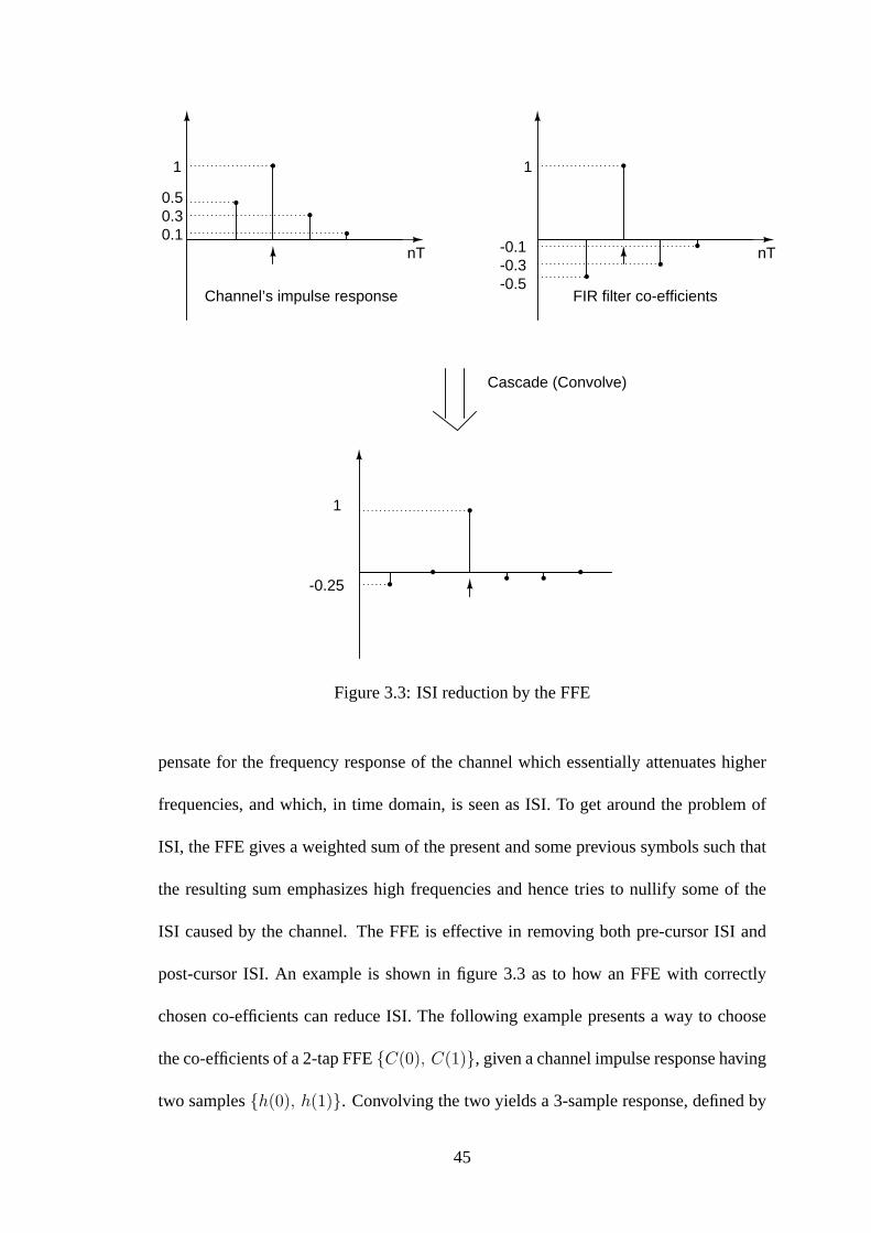
The FFE is an adjustable filter, in this case an FIR filter, that is meant to com-
44
nT
1
0.50.30.1
nT
1
-0.5-0.3-0.1
Cascade (Convolve)
FIR filter co-efficients
1
-0.25
Channel’s impulse response
Figure 3.3:ISI reduction by the FFE
pensate for the frequency response of the channel which essentially attenuates higher
frequencies, and which, in time domain, is seen as ISI. To get around the problem of
ISI, the FFE gives a weighted sum of the present and some previous symbols such that
the resulting sum emphasizes high frequencies and hence tries to nullify some of the
ISI caused by the channel. The FFE is effective in removing both pre-cursor ISI and
post-cursor ISI. An example is shown in figure3.3 as to how an FFE with correctly
chosen co-efficients can reduce ISI. The following example presents a way to choose
the co-efficients of a 2-tap FFEC(0), C(1), given a channel impulse response having
two samplesh(0), h(1). Convolving the two yields a 3-sample response, defined by
45
g(0), g(1), g(2).
g(0) = C(0)× h(0)
g(1) = C(0)× h(1) + C(1)× h(0)
g(2) = C(1)× h(1)
To get g(0) = 1 and g(1) = 0, we choose the FFE co-efficientsC(0), C(1) to
be
1
h(0),−h(1)
(h(0))2
. This leavesg(2) with a residual value of−
(h(1)
h(0)
)2
, whose
magnitude is less than
∣∣∣∣h(1)
h(0)
∣∣∣∣ because|h(1)| < |h(0)|. Using such a technique, an-tap
FFE can forcen − 1 samples to zero. Other techniques exist which choose tap co-
efficients in a way so as to reduce the mean square error and are known as minimum
mean square error techniques.
The FFE behaves as an FIR filter that de-emphasizes lower frequencies, and the
co-efficients are programmed in such a way that the frequency response is approxi-
mately the inverse of the channel response. The frequency response of the FFE output
isn’t made the exact inverse of the channel response because the channel response may
have nulls at certain frequencies and the inverse of this would mean that the FFE must
deliver infinite gain to signals at these frequencies, resulting in amplification of noise
and crosstalk in these bands. This is a basic limitation in linear equalizers. The filter
equation that depicts the FFE output is as follows.
y(n+ 1) = C−1 × x(n+ 1) + C0 × x(n) + C1 × x(n− 1) (3.1)
where y(n) is the current output, x(n+1), x(n) and x(n-1) are next, current and previous
46

bits, respectively, andC−1, C0 andC1 are the pre-cursor, mid-cursor and post-cursor
co-efficients.
Data
Vdd
Rload
Channel
g1
g0
g-1
DFF
DFF
DFF
clk(from frequency
synthesizer)
Pre-amp stages
x(n+1)
x(n)
x(n-1)
Figure 3.4:FFE block (Single-ended illustration)
The block diagram of the implemented FFE is shown in figure3.4, and the circuit
diagram given in3.5. The architecture uses the current summing technique to achieve
weighted summation of the delayed versions of the incoming data stream. Programma-
bility of the filter co-efficients is introduced by switching the bias current as shown in
figure3.6.
3.2.2 Return Loss and impedance mismatch
The pMOS current source at the FFE’s load has been incorporated to increase the
output swing, especially since the characteristic impedance of the channel comes in
parallel with the FFE’s load for AC signals, hence reducing the net resistance at the
47

Vdd
C-1 C0 C1
+
-
x(n)
+
-x(n+1)
+
-x(n-1)
out+out-
I0 I1I-1
Mn-1 Mn-1 Mn0 Mn0 Mn1 Mn1
R RMp
Ip Ip
Mn-1: 50x(300n/60n)
Mn0: 50x(3u/60n)
Mn1: 50x(900n/60n)
Mp: 52x(4u/100n)
R: 250Ω
Ip: 2.4mA - 6.8mA
I-1: 0 - 1.3mA
I0: 6mA - 11.6mA
I1: 0 - 3.5mA
C-1: 0 - 0.133
C0: 0.625 - 1.25
C1: 0 - 0.375
Vbias
IR IR
Figure 3.5:FFE circuit
48

Cx <n-1:0>
Vdd
To tail current source
I02I02n-1I0
Figure 3.6:Programmability of FFE co-efficients
G0
Channel
FFE
GLCL
log(freq)
0 dB
(G0-GL)
(G0+GL)20log
|G0-GL|C
|G0+GL|C
Reflection co-efficient
Figure 3.7:Bode plot of the reflection co-efficient
49

log(freq)
0 dB
Reflection co-efficient
GL<G0
GL=G0
GL>G0
Figure 3.8:Choosing the output conductance
output. If Ip is the common-mode current flowing through the pMOS, andIR is the
common-mode current through the resistor R, then the total peak-to-peak differential
swing at the FFE output is2(2IR+Ip)×Reff , whereReff is the effective load resistance
seen. This is because when one of the differential outputs reaches its peak value ofVDD,
then the currents through the resistor and the pMOS current source at that end goes to
zero But the tail current source still pumps in the same amount of current. Hence this
current is then diverted to the other output node through the effective load seen at that
node.
In the absence of the pMOS current source, the swing would only be4IR × Reff .
The currentIp is chosen so that the resulting drain to source resistance of the pMOS, in
parallel with the resistor R is close to, but a little less than,50Ω, in order to to satisfy the
return loss specifications. Figure3.7 illustrates the Bode plot of the return loss in the
presence of capacitive load. Figure3.8suggests graphically that the right choice for the
looking-in impedance of the FFE is slightly smaller than the characteristic impedance
50
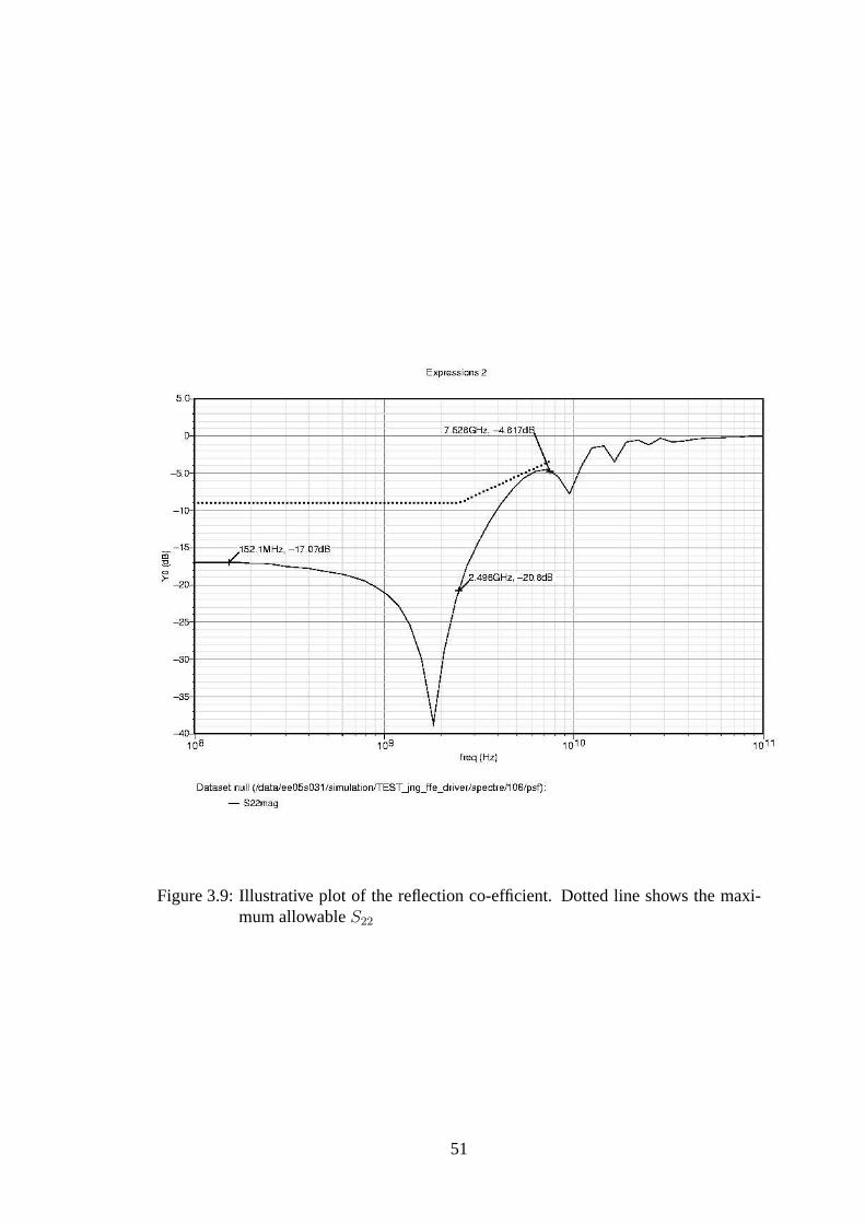
Figure 3.9:Illustrative plot of the reflection co-efficient. Dotted line shows the maxi-mum allowableS22
51

of the channel, although the impedance must not be so low that the DC reflection co-
efficient exceeds proscribed limits. The FFE is designed to have an output impedance
of about 35–40Ω.
3.2.3 Time domain understanding of ISI removal
Figures3.11and3.12provide a time domain understanding to the removal of pre
and post cursor ISI. Post cursor equalization results in an overshoot after data undergoes
a transition from 0 to 1 or vice versa, as depicted in figure3.11. When this waveform
passes through the channel with a low pass response, this overshoot pushes the channel
output to rise (or fall) faster than it would have otherwise. Similarly, pre-cursor equal-
ization causes an undershoot in voltage just before a transition in data, i.e, if data were
switching from 0 to 1, the undershoot that precedes this transition initially falls below
0 before rising to equal 1. This negative dip helps reduce the influence of the next bit
on the current bit, since they are in opposite directions. This phenomenon is observed
in figure3.12.
52
Figure 3.10:Illustrative plot of input data and output of FFE with both pre and postcursor co-efficients activated
53

Large settling timedue to previous bit
Effect of previous bitnullified by the overshoot
Transmitted into channel
Received from channel
Figure 3.11:Time domain understanding of post-cursor ISI removal
Premature transitiondue to effect of next bit
Undershoot annullseffect of next bit
Figure 3.12:Time domain understanding of pre-cursor ISI removal
54

3.3 Post-layout results
3.3.1 Area and Power Consumption
Block Number of blocks Power(mW) Area(m2)D flip flop 3 5.5 80µ× 35µ
Pre-amplifiers 2× 3 18 74µ× 25µOutput driver 1 18 93µ× 40µ
Total 42 93µ× 112µ
Table 3.1:Power and area used up by the FFE’s constituent blocks
3.3.2 10GBASE-KR specifications
The FFE, being the final stage of the transmitter before data is directed into the
channel, has to conform to a range of specifications dictated by IEEE 802.3ap Ethernet
Backplane Task Force (10GBASE-KR). The standard requires a three tap FFE, with one
pre-cursor and one post-cursor tap. Table3.2 shows the range and resolution of each
tap.
Tap Maximum Minimum Resolution (bits)Pre-cursor (C−1) 0 -0.133 3
Center-cursor (C0) 1.25 0.625 5Post-cursor (C1) 0 -0.375 4
Table 3.2:Range and resolution of FFE taps
Figure 3.13 shows the output waveform of the transmitter when both post and
pre-cursor taps are activated. The standard now defines two terms,Rpre =v3
v2
, and
Rpre =v1
v2
. Table3.3defines the waveform requirements for different co-efficient com-
binations. The transmitter also needs to satisfy differential as well as common mode
55

Figure 3.13:Transmitter output waveform (IEEE 802.3ap(2007))
C1 C0 C−1 Rpre Rpst v2 mVdisabled minimum disabled 0.9 to 1.1 0.9 to 1.1 220 to 330disabled maximum disabled 0.95 to 1.05 0.95 to 1.05 400 to 600
minimum minimum disabled - 4.00 (min) -disabled minimum minimum 1.54 (min) - -
Table 3.3:Transmitter output waveform requirements related to coefficient status (IEEE802.3ap(2007))
56
return loss specifications seen in figures3.15and3.16for all valid output levels. The
test equipment used to measure the return loss is as seen in figure3.14. The reference
impedance for measuring differential return loss is100Ω, and that for measuring com-
mon mode return loss is25Ω. The maximum allowable differential and common mode
return losses is seen in figures3.15and3.16.
Figure 3.14:Transmit test fixture for 10GBASE-KR (IEEE 802.3ap(2007))
Simulation results for the laid-out FFE show that it meets the swing requirements
referred to in the first two rows of table3.3, which relate to the FFE output swing
when only the center tap is activated. But the ratiosRpre andRpst fall short of the
requirements given in the last two rows. The performance was seen to be better with
inductive load at the output of the FFE, since it enables higher swings and hence higher
Rpre andRpst ratios. But this improvement in swing performance comes at the cost of
poorer return loss, and hence the inductive load was done away with. Since the FFE is
a programmable equalizer and not an adaptive equalizer, the design of the FFE did not
necessitate the need for the backplane model. And without the transmission line model
57
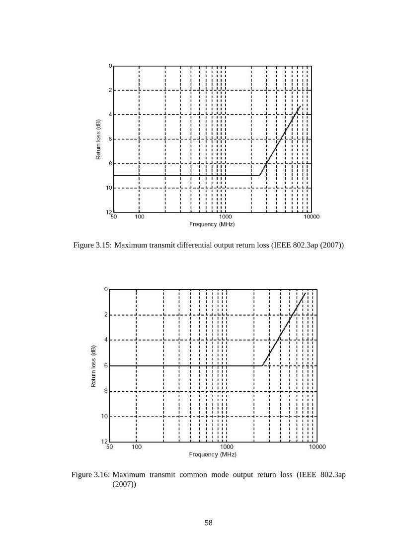
Figure 3.15:Maximum transmit differential output return loss (IEEE 802.3ap(2007))
Figure 3.16:Maximum transmit common mode output return loss (IEEE 802.3ap(2007))
58
and the values to be assigned to the co-efficients of the FFE, it makes no sense to plot
the eye diagram at the output of the FFE.
As for return loss, the FFE meets the relatively laid-back specifications of common
mode return loss as was defined in figure3.16. Specification for differential mode
return loss proved more tricky to meet, with most corners disappointing after 6 GHz.
But, it must be noted that the model used for simulation is essentially inadequate for
frequencies above about 3 GHz even, since, at these very high frequencies, the board
and test equipment greatly influence measurements. Figures3.17 and3.18 show the
return loss before and after layout, for the maximum absolute magnitudes of the co-
efficients. It can be observed that in post-layout simulation, the reflection co-efficient
begins to increase beyond 1 GHz, unlike in the case of the simulations conducted for
the schematic design, in which case the rise occurs around 2 GHz. This is because the
additional parasitic capacitance added at the FFE’s output after layout causes the zero
to appear earlier, as was seen in figure3.7.
The following tables show the detailed results obtained from post-layout simulation
of the FFE.
Cases
1. C0 minimum;C−1 andC1 disabled.
2. C0 maximum;C−1 andC1 disabled.
3. C0 minimum;C1 minimum;C−1 disabled.
4. C0 minimum;C−1 minimum;C1 disabled.
59
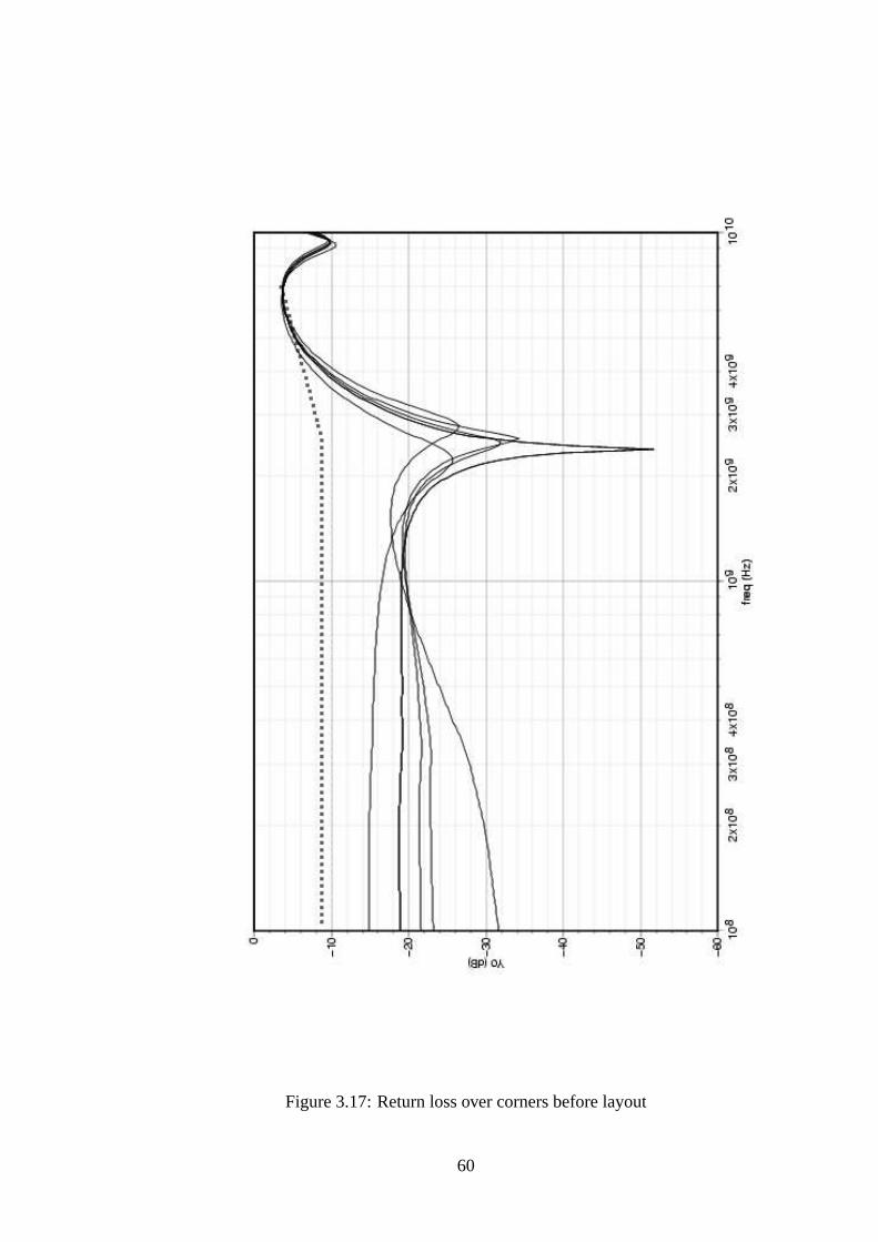
Figure 3.17:Return loss over corners before layout
60

Figure 3.18:Return loss over corners post-layout
61

Figure 3.19:Layout of the FFE
62

Case Misbehaving corners for S22
(Common mode)1 None2 None3 None4 None
Table 3.4:Simulation results for common mode return loss
Case Misbehaving corners forS22 (Dif-ferential)
Desired value Value obtained
1 Most corners S22 < −3.2745 dB forf = 7.5 GHz
∼ 2.5 dB
2 Most corners S22 < −3.2745 dB forf = 7.5 GHz
∼ 2.5 dB
3 Most corners S22 < −3.2745 dB forf = 7.5 GHz
∼ 2.5 dB
4 Most corners S22 < −3.2745 dB forf = 7.5 GHz
∼ 2.5 dB
Table 3.5:Simulation results for differential mode return loss
Case Misbehaving corners for tran-sient signal
Desired value Value obtained
1 None - -2 None - -3 Most corners Rpst > 4 3.3 ≤ Rpst ≤ 44 Most corners Rpre > 1.54 1.2 ≤ Rpre ≤ 1.44
Table 3.6:Simulation results for output transmit signal
63

CHAPTER 4
Multiplexer
4.1 Introduction
A multiplexer or a MUX is a device that selects one of many input lines and directs
it into a single output line. The multiplexer on the designed transmitter clubs 32 data
channels, each of 156.25 Mbps, into a single stream of 10 Gbps before transmitting it
over the channel. The streams are multiplexed cyclically in a sequential manner. This
datastream is de-multiplexed back into 32 channels by a complementary demultiplexer
at the receiver end.
4.2 Design aspects
The 32x1 MUX is implemented partly in differential current mode logic and partly
using single-ended CMOS logic. 32x1 MUX uses 5 select lines driving 5 layers of
2x1 MUXs with progressively increasing speed of operation as we move from input to
output. CMOS logic is used for the layers operating at less than 2.5Gbps. 2x1 MUX
implemented in CMOS and CML are shown in figures4.3and4.2 respectively. A 4x1
MUX built from these 2x1 MUX blocks is shown in figure4.1. The latches are needed
to ensure that data doesn’t change when MUX is sampling it. The convention used in
the figure is the latch with the bubble holds data at negative cycle of clock while the one
without holds data at the clock’s positive cycle.

0 1
sel1
sel1
sel1
In0
In2 In1
In3
sel1
0 1
sel1
sel1
sel1
sel1
0 1
sel0
sel0
sel0
sel0
2:1
MU
X
2:1
MU
X
2:1
MU
X
latch latch
latch
latch latch
latch
latch latch
latch
Figure 4.1:4x1 MUX
65

Vdd
seln selp
D0p D0n D1p D1n
outn outp
R R
I
M1a M1b
M0a M0b
M2a M2b
CML0 (Refer figure 4.4) CML1
I 300µA 150µA
M0 8x(500n/60n) 4x(500n/60n)
M1, M2 4x(500n/60n) 2x(500n/60n)
R 2.6kΩ 5.2kΩ
Figure 4.2:2x1 CML MUX
Vdd
D0 D1
selsel
sel
sel D0
D1
Mna Mnb
Mnc Mnd
Mpa
Mpc
Mpb
Mpd
Mn : 2x(200n/60n)
out
Mp : 6x(200n/60n)
Figure 4.3:2x1 CMOS MUX
66

sel4 sel3 sel2 sel1 sel0
32 channels 16x(2:1)
MUXsCMOS
8x(2:1)CMOSMUXs
4x(2:1)CMOSMUXs
2x(2:1)CML1
MUXs
(2:1)CML0
MUX
(5GHz)(2.5GHz)(1.25GHz)(0.625GHz)(0.3125GHz)
Figure 4.4:Layered architecture
D
clk
Q
Qsel3
sel4
Figure 4.5:Illustration of select line generation
67
The last two layers operating at 10Gbps and 5Gbps are implemented in differential
CML, while the slower stages are in single-ended CMOS. Static power consumed by
the CML layers of the 32x1 MUX is2.4 mW. The select lines of the MUX (sel0 -
sel5) vary between 5 GHz and 0.3125 GHz, as is seen in figure4.4 with every select
line differing in frequency by a factor of two from its neighbours. Figure4.5 illustrates
how the select lines are generated. All these frequencies are already available within
the frequency synthesizer’s divider, and hence the select lines are extracted from the
synthesizer through buffers. The power consumed by the buffers is about2.4 mW,
resulting in an overall power consumption of4.8 mW for the entire MUX.
68
CHAPTER 5
Clock and Data Recovery Circuit (CDR)
5.1 Introduction
High speed digital data streams are transmitted without an accompanying clock so
as to reduce power. The receiver, hence, needs to generate an appropriate clock which
is phase-aligned to the received data bits in order to facilitate reliable recovery of data.
This process is referred to as clock and data recovery, and the circuit that performs this
operation is called a clock and data recovery circuit (CDR). Data recovery is performed
using a phase-locked loop (PLL) or a delay locked loop (DLL). While a PLL, like the
one designed to be used as a frequency synthesizer as was seen in chapter2, houses an
internal oscillator in its loop, a DLL is characterized by the absence of such an oscillator
to achieve phase lock. Instead, the main component of a DLL is a delay chain composed
of many delay gates connected in cascade, which produce delayed versions of an input
reference clock, the most suitable of which maybe used to clock and recover data.
The basic architecture of the designed CDR is seen in figure5.1. The CDR uses
the forwarded clock from the transmitter and generates multiple phases of clock from
this using a delay locked loop, which, in this case generates 6 equally spaced phases
by means of three identical delay cells. The locking is ensured by tying the end of the
last delay cell to a simple phase detector which in turn controls the current flowing into
the delay cell, and hence controls the delay introduced by each delay cell. While it
is possible to choose the most optimum phase out of the available six phases to clock

10GHz signalfrom TX
0o/180o
60o /2
40o
120o /3
00o
180o /0
o
i/p
o/p1 o/p2 o/p3
DLL
MUX
up dn
+ - + -A BPhase interpolator
Alexander PD
DigitalAccumulator
Select lineControl
PI weightsControl
ReceivedData
10GHz clock from
phase interpolator
Figure 5.1:Architecture of the clock/data recovery circuit
the data, it must be noted that successive delayed signals differ by60 and so even
the most optimal clock phase transition maybe far from the center of the tracked data
bit. This creates a need for better phase resolution, or, in other words, more phases of
the transmitted clock. The phase interpolator achieves precisely this. When a phase
interpolator is fed two signals of the same frequency but different phases, it generates
an output signal having a phase that is between that of its input signals. The interpolator
designed is capable of generating 16 nearly equidistant phases by weighted summation
of its two input signals, theweightscalculated by an appropriate digital circuitry, as will
be discussed in section5.3 later in this chapter.
70

5.2 Delay Locked Loop (DLL)
The architecture of the designed DLL is seen in figure5.2. The combined delay
produced by the three delay cells is adjusted to be equal toT
2, T being the period of the
incoming clock signal. This is done by locking the output of the third delay cell to the
inverted transmitter clock signal by means of a phase detector, whose output drives a
digital circuit which in turn controls the delay of each cell by increasing or decreasing
the current consumed by the delay cells. The phase detector (PD) used is a simple non-
linear detector, seen in figure5.3, which detects which of its two input signals is ahead,
and digital circuit takes appropriate measures to reduce the phase offset between the
two signals. The process of locking is seen in figure5.4. The phase detector continues
to provide alternate up/dn signals which results in chopping even after lock is achieved.
The figure5.4 shows that the DLL locks when the number of current sources (each
20µA) turned on is between 29 and 30.
A potential problem in DLLs is that if the three delay cells were to produce a com-
bined delay of3T
2, and not
T
2, the phase detector would be unable to pick the error and
would naively establish lock, since the two are indistinguishable. This is a problem be-
cause, now each cell delays the transmitter clock byT
2(or 180) instead of the desired
T
6(or 60). Fortunately, in the current design, the delay cells do not cause a delay of
more than 24 ps, even in the worst case, whereas a false lock would require each cell to
delay the signal by as much as 50 ps.
The delay cell’s implementation is shown in figure5.5. The delay is controlled by
varying the amount of current driving the differential pair by means of a digital control
element. The power consumption of each delay cell doesn’t exceed1.8 mW, inclusive
71

+
-
10GHz signalfrom TX
0o/180oD1 D2 D3
+
+
-
-
A
B
up
dn
DigitalDelayControl
60o/240o 120o/300o 180o/0o
180o/0o
BBPD1
Figure 5.2:DLL architecture
VLCosc
VDLL,out
upD
clk
Q
D
clk
Q
VLCosc
VDLL,out dn
Figure 5.3:Simple phase detector used to lock the DLL
72

Figure 5.4:DLL tracking behaviour
73

of the biasing currents. The minimum resolution of current possible is20µA, and the
design uses about 32 resolvable current steps over and above a minimum level of current
required in order to keep the cell functioning even if the control input drops to zero.
The delay produced by the delay cells is so small in some corners (as low as 12 ps
per cell instead of the desired 16.7 ps) that there is a need to introduce changes in the
circuit that increase the delay. This is done so by introducing a right half plane zero,
which adds to the delay in the form of capacitorCdelay, seen in figure5.6. The capacitor
Cdelay is switched into play if the delay cell’s current consumption drops below a pre-
defined value (which implies that the circuit is striving to achieve more delay, and the
introduction of a right half plane zero eases this process).
Vdd
Vdd
+
-
vin
+
-
vout+ -
vcm,ref
Cc
DigitalControl
vcmfb
I0I0
Mmirr Mtail
Mna Mnb
Mpa Mpb
Rcm Rcm
I0 : 20µA
Mmirr : 64x(200n/60n)
Mtail : 192x(200n/60n)
Mn : 96x(200n/60n)
Mp : 96x(400n/60n)
CC : 30fF
RCM : 10kΩ
Figure 5.5:Individual delay cell in the DLL
The D-flip flops used in for the DLL’s phase detector are designed using CML (cur-
74
Vdd
vout+ -
Cc
Cdelay Cdelay
Delay controllingcurrent
vi+vi-
vcmfb
vcm
Rcm Rcm
Mpa Mpb
Mna Mnb
Mp : 96x(400n/60n)
Mn : 96x(200n/60n) CC : 30fF
RCM : 10kΩ Cdelay : 10fF
Figure 5.6:Delay cell with option to increase delay
rent mode logic) latches. Any practical phase detector (PD) has a dead zone. This is the
region where the PD’s input signals are so close together in phase that the PD becomes
incapable of determining which signal leads which. This is more of a problem if the
inputs are sinusoidal than if they are pulse-shaped, as a sinusoidal signal takes longer
to reach the amplitude that can be reliably detected by the PD. The bang-bang detector
used in the DLL too suffers from a dead-zone. The dead zone can be countered by
reducing the delay from the input to the output of the PD’s latch, and also by increasing
the gain so that any change in the input is immediately reflected and even amplified at
the output, and hence easier to register by the the latching process than otherwise. Both
of the afore mentioned qualities are salient features of a left half plane zero placed a
little before the frequency of operation, and this is achieved by the capacitorCspeed seen
in figure5.7. The dead-zone time difference is reduced to about3.5 ps (or about10),
75

as against a dead-zone of7 ps (or about20) without it (for sinusoid inputs).
A zero could also have been introduced by means of an inductor in series with the
resistive load, but for the small currents used in the latch, a huge inductor of over 10 nH
is needed to see any effect, and large inductors mean a very large area.
Vdd
CspeedData+ Data-
clk+ clk-
I0
M1a M1b
M2a M2b M2c M2d
R R
M1 : 20x(240n/60n)
M2 : 20x(240n/60n) Cspeed : 10fF
R : 1.75kΩ I0 : 550µA
Figure 5.7:Latch used in the DLL phase detector’s D-flip flop
5.3 Phase Interpolator
The DLL generates only 6 phases of clock, and at a given time none of then maybe
in phase with the data received. To get the right phase of clock, we need a circuit that
generates any phase lying between the available phases of clock. A circuit that performs
76
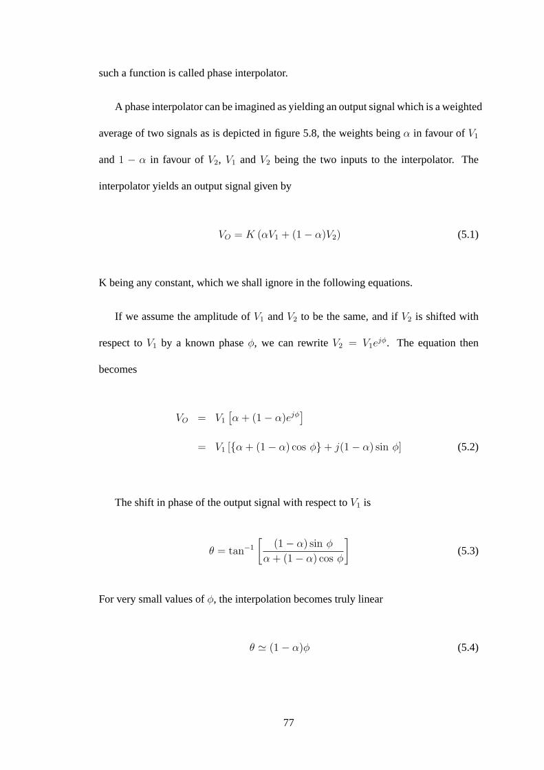
such a function is called phase interpolator.
A phase interpolator can be imagined as yielding an output signal which is a weighted
average of two signals as is depicted in figure5.8, the weights beingα in favour ofV1
and1 − α in favour of V2, V1 andV2 being the two inputs to the interpolator. The
interpolator yields an output signal given by
VO = K (αV1 + (1− α)V2) (5.1)
K being any constant, which we shall ignore in the following equations.
If we assume the amplitude ofV1 andV2 to be the same, and ifV2 is shifted with
respect toV1 by a known phaseφ, we can rewriteV2 = V1ejφ. The equation then
becomes
VO = V1
[α + (1− α)ejφ
]
= V1 [α + (1− α) cos φ+ j(1− α) sin φ] (5.2)
The shift in phase of the output signal with respect toV1 is
θ = tan−1
[(1− α) sin φ
α + (1− α) cos φ
](5.3)
For very small values ofφ, the interpolation becomes truly linear
θ ' (1− α)φ (5.4)
77
Vdd
αI (1−α)I
V1
Vout = αV1+(1-α)V2IR
V2
R
(b)
Phase Interpolator Analogy
(a)
V1 V2
(1−α)R αR
Vout = αV1+(1-α)V2
Figure 5.8:Circuits depicting operation of a phase interpolator
Figures5.9 and5.10 make it clear that the smaller the phase difference between the
signals fed to the phase interpolator, the more linear its output phase change with weight
α. In the equations where we derived the phase of the interpolator’s output, we chose
to assume that the amplitude of the incoming signals is equal, which might not always
be true, although the CDR can specially designed so as to ensure this, as has been done
in this design. If the signals were to be of different amplitudes but same phase, the
interpolator would see one signal rise faster than the other and mistake the former to be
ahead in phase than its slower counterpart. The magnitude of phase difference would
depend on the voltage sensitivity of the phase interpolator, greater the sensitivity lesser
the phase offset.
The resistor (or capacitor) divider shown in figure5.8(a) isn’t used due to practical
constraints of loading and swing. Instead the architecture of the phase interpolator used
78

Figure 5.9:Interpolator performance for input signals differing by60
79

Figure 5.10:Interpolator performance for input signals differing by150
80
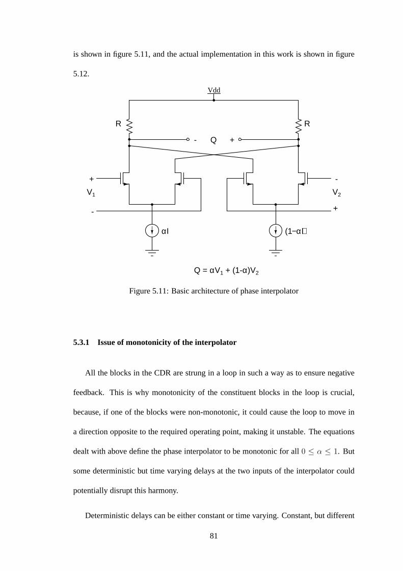
is shown in figure5.11, and the actual implementation in this work is shown in figure
5.12.
+-
V2
+
-
Vdd
R R
Q
αΙ
V1
+
-
(1−α)Ι
Q = αV1 + (1-α)V2
Figure 5.11:Basic architecture of phase interpolator
5.3.1 Issue of monotonicity of the interpolator
All the blocks in the CDR are strung in a loop in such a way as to ensure negative
feedback. This is why monotonicity of the constituent blocks in the loop is crucial,
because, if one of the blocks were non-monotonic, it could cause the loop to move in
a direction opposite to the required operating point, making it unstable. The equations
dealt with above define the phase interpolator to be monotonic for all0 ≤ α ≤ 1. But
some deterministic but time varying delays at the two inputs of the interpolator could
potentially disrupt this harmony.
Deterministic delays can be either constant or time varying. Constant, but different
81
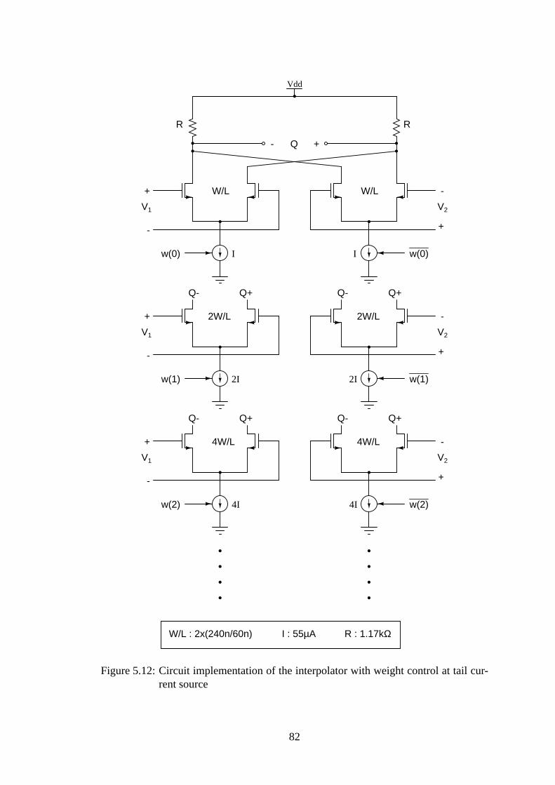
+-
V2
+
-
Vdd
R R
Q
I w(0)
W/L
I
V1
+
-
W/L
w(0)
2I
V1
+
-
2W/L
w(1)
Q- Q+
4I
V1
+
-
4W/L
w(2)
Q- Q+
V2
+
-
2I w(1)
2W/L
Q+Q-
V2
+
-
4I w(2)
4W/L
Q+Q-
W/L : 2x(240n/60n) I : 55µA R : 1.17kΩ
Figure 5.12:Circuit implementation of the interpolator with weight control at tail cur-rent source
82

time delays at the two inputs can be accounted for as phase offset between the input
signals. This would change the resolution at the interpolator output but still maintains
monotonicity. Constant, and equal time delay at the inputs doesn’t alter the phase dif-
ference in any way, and the designer would ideally want to ensure such a scenario. But a
more torrid scene is to have the input delays vary based on the weightage of the incom-
ing signal, and such a situation does arise in the interpolator design undertaken in this
work. Figure5.12shows that the input signal sees a load proportional to the weightage
it receives. If the increase in the delay seen by the interpolator’s input signal with every
unit increase in its weightage were4φ, we can define it as follows
φ ∝ 2π
TO
RC
φ+4φ ∝ 2π
TO
RC
(1 +
4CC
)
⇒4φ ∝ 2π
TO
R4 C (5.5)
whereφ is the original phase delay, R and C are the effective resistance and capacitance
at the input nodes,4C is the increment in capacitance at the node due to the added
unit weight,4φ is the incremental phase delay due to this additional load, andTO is
the time period of the signal. This equation only demonstrates that the delay added for
every additional weight can be approximated to be equal too. Figure5.13depicts the
delays encountered at inputsφ1 andφ2.The linearized output of the phase interpolator
(ψO) is now given by the following equation
ψo =[φ+ (N − k)4 φ] (N − k) + [φ+ φo + k.4 φ] k
N
= φ+k
Nφo +
4φN
[k2 + (N − k)2
](5.6)
83

here,φo is the required difference in phase between inputsφ1 andφ2, N is the maxi-
mum weightage that could possibly be assigned to an input signal, and k is the assigned
weight such thatα =k
N, α being the weight generated by the digital logic block that
defines the interpolator weights, andφ is the common delay (or phase offset) experi-
enced by both the input signals.
From the above equation, we notice that, if it weren’t for the weight dependent delay
4φ, the curve shows a constant slope ofφo
N, and is hence monotonic. But, inclusive
of 4φ, the slope of the curve could hit zero, indicating a possible loss of monotonicity.
This is seen in the following equation where we derive the slope to be
∂ψo
∂k=φo
N+ 2(2k −N)
4φN
(5.7)
For a given value of k, the slope goes to zero at4φ =φo
2(N − 2k), and the second
derivative ofψo confirms this point to be the minima. It must also be noted that the
minima doesn’t occur fork ≥ N
2. For the interpolator output to be monotonic, this
minima must lie atk = 0, which requires that
4 φ <φo
2N(5.8)
For this design whereφo = 60 andN = 15, we can calculate4φ < 2 which is about
0.56 ps for a 10 GHz signal.
The magnitude of4φ hence puts a constraint on the maximum achievable resolution
of the phase interpolator (in other words, constraint on the maximum possible value of
N). Figure5.14attempts to shed light on why the interpolator’s output phase reduces
84

instead of increasing with increase in weight. This is so because, as we increase k,
although we expect inputsφ1 andφ2 to remain stable,φ1 experiences less and less
delay due to falling weights at its end, and the output phase followsφ1 more closely
than it followsφ2 as long as(N − k) > k. This results inφout falling rather than rising.
While increasing k brings about reduction inφ1 delay, it causes increase in delay
at inputφ2, and fork >N
2, φout more closely followsφ2 and so always rises with
increasing k, which explains why no minima can occur fork >N
2.
PI
φ1
φ2
φout
(N-k)∆C
(k)∆C
weight = α = k/N
φ1(N-k) + φ2kN
φ
φ + φo
φ + (N-k)∆φ
φ + φo + k∆φ
Figure 5.13:Weight dependent delay at interpolator input
5.3.2 Phase Interpolator design and simulation results
The simplest design modification that can be made to prevent delay modulation
at the input with change in weights is to connectφ1 andφ2 to another similar phase
interpolator but with inputs switched. This would result in both inputs seeing the same
input load given byk4 C + (N − k)4 C = N 4 C. This is portrayed in figure5.15.
Another design aspect is to determine where to incorporate the digital control switches
which aid in increasing or reducing the weightage allotted to the inputs. While figure
5.12shows interpolator weights being set by tail current, the phase versus weight plot
85
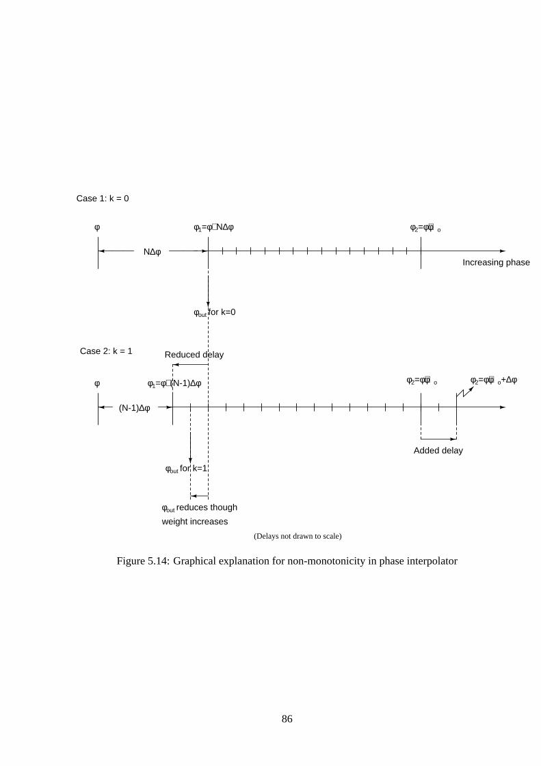
Case 1: k = 0
φ
N∆φ
φ1=φ+N∆φ φ2=φ+φo
φ φ2=φ+φo
Case 2: k = 1
(N-1)∆φ
φ1=φ+(N-1)∆φ
Increasing phase
φ2=φ+φo+∆φ
φout for k=0
φout for k=1
φout reduces though
weight increases
Added delay
Reduced delay
(Delays not drawn to scale)
Figure 5.14:Graphical explanation for non-monotonicity in phase interpolator
86

PI1
φ1
φ2
φout1
(N-k)∆C
(k)∆C
weight = α = k/N
φ1(N-k) + φ2kN
φ
φ + φo
PI2
φ1
φ2
(k)∆C
(N-k)∆C
φ2(N-k) + φ1kN
φ + φo + N∆φ
φ + N∆φ
φout2
Figure 5.15:Design modification to remove weight dependent delay
turns out to be better for an interpolator with controlling switches at its input terminals
rather at the tail transistor’s gate, although the former allows for the usage of minimum
sized switches. Figure5.16 shows the behaviour of an interpolator with tail current
control. This architecture suffers due to unwelcome coupling between the input signal
and the interpolator output through the gate to drain capacitanceCGD of the input tran-
sistor pair. Consider for instance thatk = 0 which means that inputφ2 must have no
influence on the output signal. But though the tail current source atφ2’s end is turned
off, φ2 seeps into the output throughCGD and distorts it, which in the plot o figure5.16
is seen an a droop in the phase output which then fails to follow the ideal curve shown
in red. The implemented architecture of the interpolator is seen in figure5.17. In this
circuit, once the switch is turned off, input and output are completely isolated from each
other. The performance of this architecture is shown in figure5.18.
87

0 5 10 150
10
20
30
40
50
60
weight
angl
e
Delay vs Weight for tail node controlled phase interpolator
Expected delayObtained delay
Figure 5.16:Performance of interpolator with tail current control
88
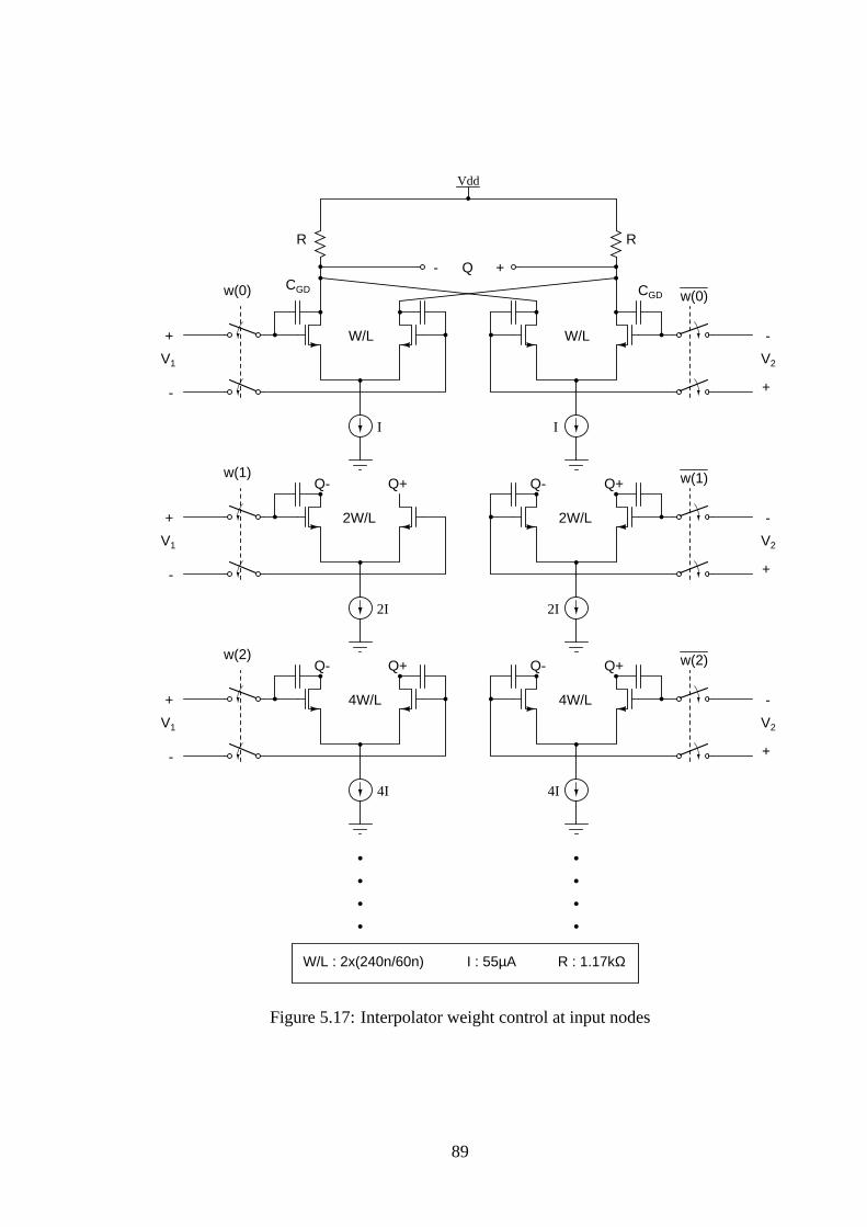
+-
V2
+
-
Vdd
R R
Q
I
w(0)
W/L
I
V1
+
-
W/L
w(0)
2I
2W/L
Q- Q+
4I
4W/L
Q- Q+
2I
2W/L
Q+Q-
4I
4W/L
Q+Q-
V1
+
-
w(1)
V1
+
-
w(2)
V2
+
-
w(1)
V2
+
-
w(2)
CGD CGD
W/L : 2x(240n/60n) I : 55µA R : 1.17kΩ
Figure 5.17:Interpolator weight control at input nodes
89
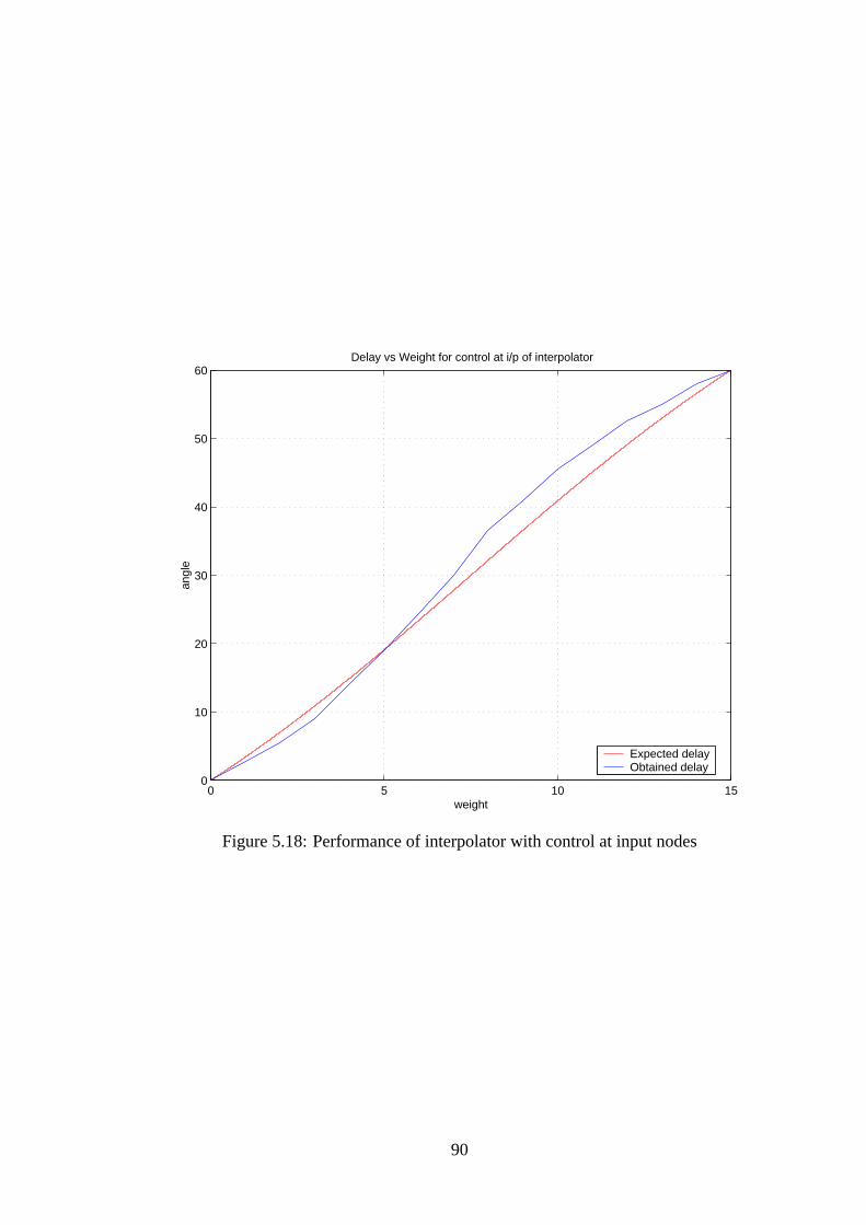
0 5 10 150
10
20
30
40
50
60
weight
angl
e
Delay vs Weight for control at i/p of interpolator
Expected delayObtained delay
Figure 5.18:Performance of interpolator with control at input nodes
90
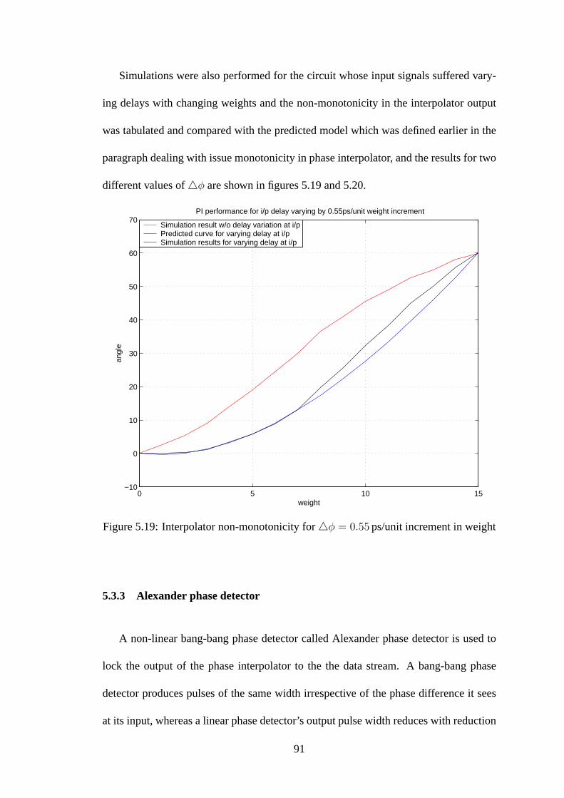
Simulations were also performed for the circuit whose input signals suffered vary-
ing delays with changing weights and the non-monotonicity in the interpolator output
was tabulated and compared with the predicted model which was defined earlier in the
paragraph dealing with issue monotonicity in phase interpolator, and the results for two
different values of4φ are shown in figures5.19and5.20.
0 5 10 15−10
0
10
20
30
40
50
60
70
weight
angl
e
PI performance for i/p delay varying by 0.55ps/unit weight increment
Simulation result w/o delay variation at i/pPredicted curve for varying delay at i/pSimulation results for varying delay at i/p
Figure 5.19:Interpolator non-monotonicity for4φ = 0.55 ps/unit increment in weight
5.3.3 Alexander phase detector
A non-linear bang-bang phase detector called Alexander phase detector is used to
lock the output of the phase interpolator to the the data stream. A bang-bang phase
detector produces pulses of the same width irrespective of the phase difference it sees
at its input, whereas a linear phase detector’s output pulse width reduces with reduction
91

0 5 10 15−10
0
10
20
30
40
50
60
70
weight
angl
e
PI performance for i/p delay varying by 1ps/unit weight increment
Simulation result w/o delay variation at i/pPredicted curve for varying delay at i/pSimulation results for varying delay at i/p
Figure 5.20:Interpolator non-monotonicity for4φ = 1 ps/unit increment in weight
92
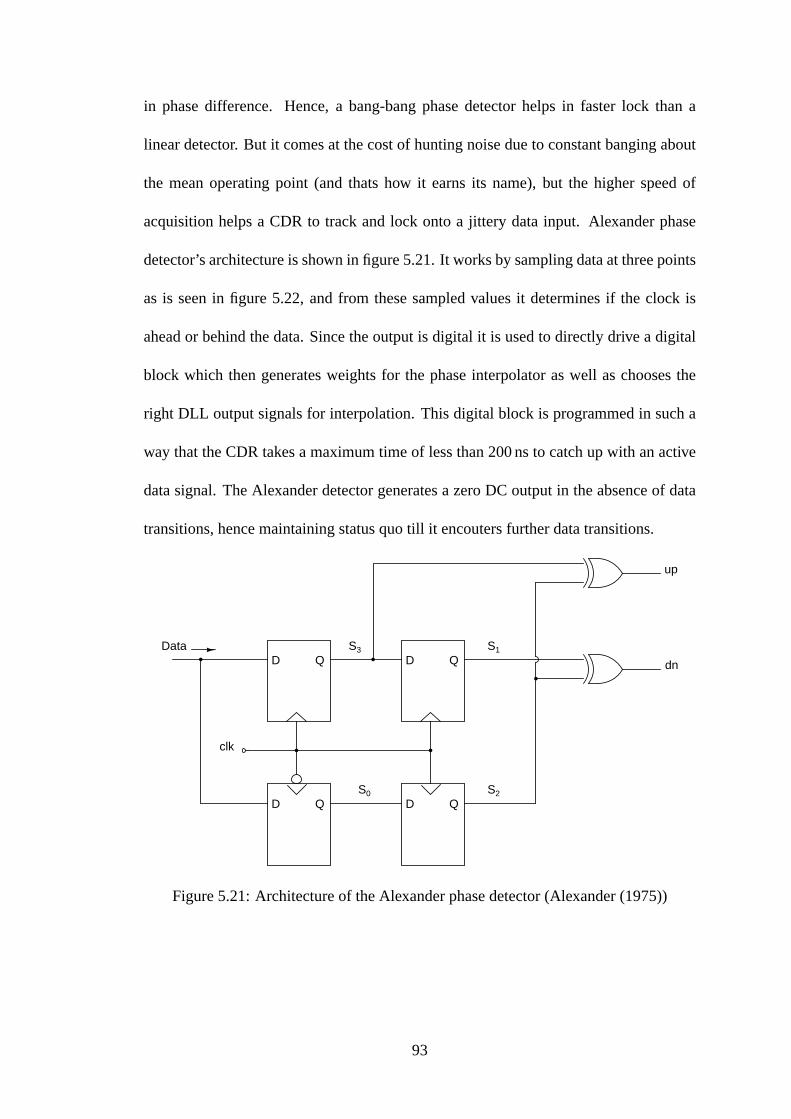
in phase difference. Hence, a bang-bang phase detector helps in faster lock than a
linear detector. But it comes at the cost of hunting noise due to constant banging about
the mean operating point (and thats how it earns its name), but the higher speed of
acquisition helps a CDR to track and lock onto a jittery data input. Alexander phase
detector’s architecture is shown in figure5.21. It works by sampling data at three points
as is seen in figure5.22, and from these sampled values it determines if the clock is
ahead or behind the data. Since the output is digital it is used to directly drive a digital
block which then generates weights for the phase interpolator as well as chooses the
right DLL output signals for interpolation. This digital block is programmed in such a
way that the CDR takes a maximum time of less than 200 ns to catch up with an active
data signal. The Alexander detector generates a zero DC output in the absence of data
transitions, hence maintaining status quo till it encouters further data transitions.
clk
Data
D
D D
D
Q
Q Q
Q
up
dn
S1
S2
S3
S0
Figure 5.21:Architecture of the Alexander phase detector (Alexander(1975))
93
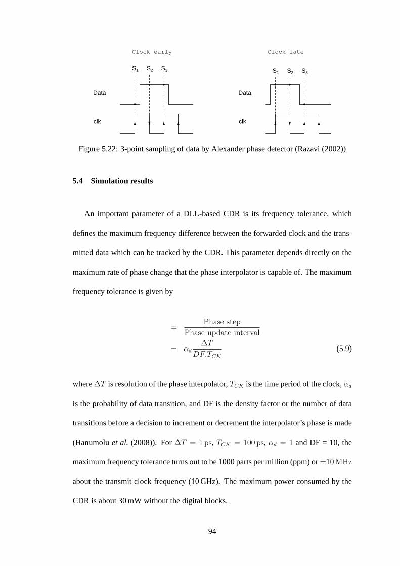
Data
clk
Clock early
S1 S2 S3
Data
clk
S1 S2 S3
Clock late
Figure 5.22:3-point sampling of data by Alexander phase detector (Razavi(2002))
5.4 Simulation results
An important parameter of a DLL-based CDR is its frequency tolerance, which
defines the maximum frequency difference between the forwarded clock and the trans-
mitted data which can be tracked by the CDR. This parameter depends directly on the
maximum rate of phase change that the phase interpolator is capable of. The maximum
frequency tolerance is given by
=Phase step
Phase update interval
= αd∆T
DF.TCK
(5.9)
where∆T is resolution of the phase interpolator,TCK is the time period of the clock,αd
is the probability of data transition, and DF is the density factor or the number of data
transitions before a decision to increment or decrement the interpolator’s phase is made
(Hanumoluet al. (2008)). For ∆T = 1 ps, TCK = 100 ps, αd = 1 and DF = 10, the
maximum frequency tolerance turns out to be 1000 parts per million (ppm) or±10 MHz
about the transmit clock frequency (10 GHz). The maximum power consumed by the
CDR is about 30 mW without the digital blocks.
94

There could be jitter in the clock because of hunting noise, wherein the phase-
interpolator switches between two neighbouring phases if the required clock lies be-
tween these two discrete phases of clock. The jitter in such a case doesn’t exceed 1.2 ps
rms. The hunting behaviour of the phase interpolator is seen in figure5.23. The Y-axis
gives the phase (from among the 16 available phases) selected to recover data.
Figure 5.23:Phase interpolator hunting noise
95

CHAPTER 6
Modelling of on-chip inductors
6.1 Introduction
The architecture of the transceiver chosen for our work uses only a single on-chip
inductor in the form of the resonance inductor in the LC-VCO of the frequency synthe-
sizer at the transmitter. But if the CDR at the receiver were based on a PLL instead of
a DLL, it might save on the extra power required to forward the high frequency clock
all the way from the transmitter to the receiver through a series of buffers. A PLL re-
quires a VCO of its own, and this maybe implemented as a ring oscillator or an LC
oscillator, the latter generating a lesser phase noise than the former. But the presence of
two inductors (one each from the frequency synthesizer and the CDR), with both oper-
ating at almost the same frequency, can easily result in mutual interference, of greater
concern being the interference due to the CDR on the frequency synthesizer, since a fre-
quency synthesizer must typically meet much tighter jitter specifications than a CDR.
This necessitates more thought to be put into the placement of the inductors.
6.2 Theory
While a frequency synthesizer is designed to be a very stable frequency source, a
CDR is designed to react fairly rapidly to a jittery and drifting datastream. Even if the
CDR were to generate an ideal, unwavering clock, this would still result in periodic
jitter at the frequency synthesizer’s clock if the two clocks differed in frequency. Add
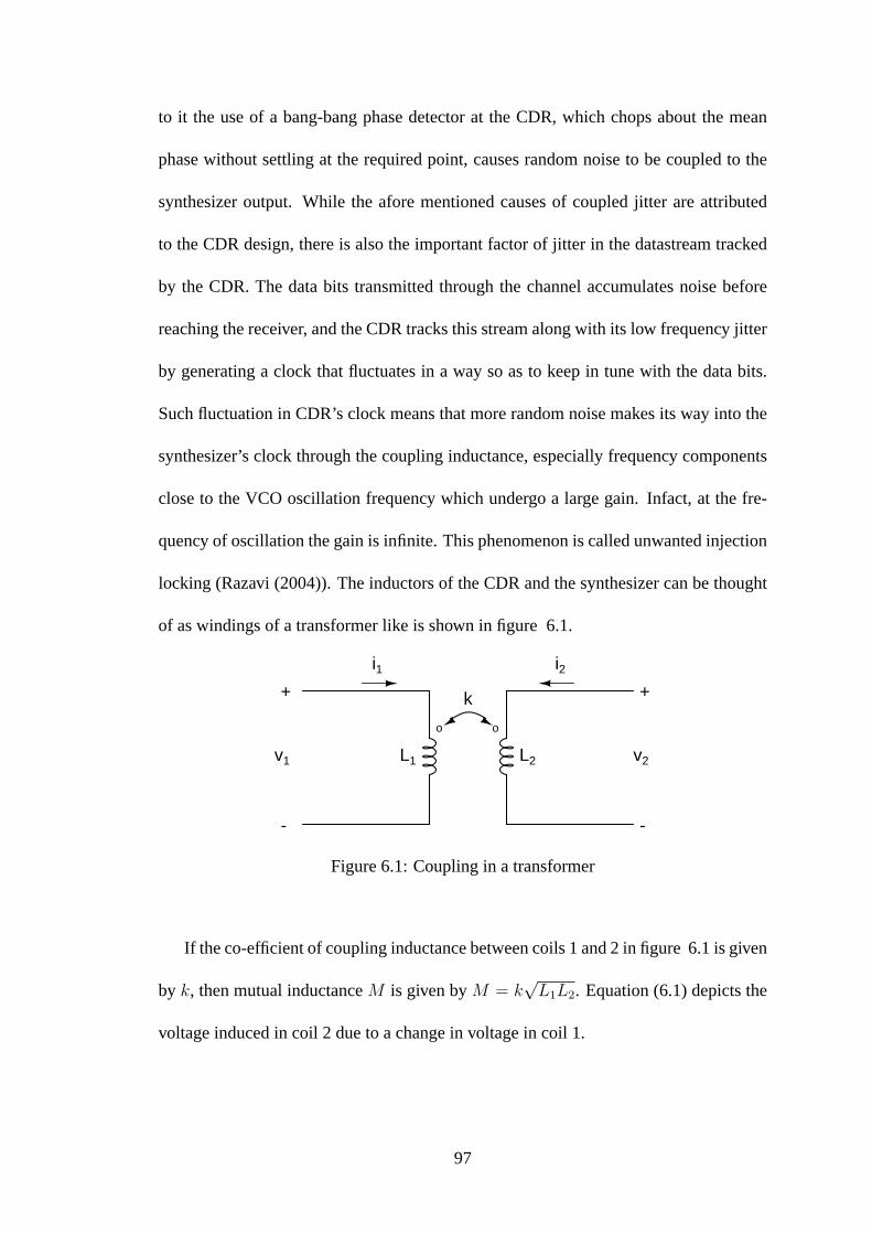
to it the use of a bang-bang phase detector at the CDR, which chops about the mean
phase without settling at the required point, causes random noise to be coupled to the
synthesizer output. While the afore mentioned causes of coupled jitter are attributed
to the CDR design, there is also the important factor of jitter in the datastream tracked
by the CDR. The data bits transmitted through the channel accumulates noise before
reaching the receiver, and the CDR tracks this stream along with its low frequency jitter
by generating a clock that fluctuates in a way so as to keep in tune with the data bits.
Such fluctuation in CDR’s clock means that more random noise makes its way into the
synthesizer’s clock through the coupling inductance, especially frequency components
close to the VCO oscillation frequency which undergo a large gain. Infact, at the fre-
quency of oscillation the gain is infinite. This phenomenon is called unwanted injection
locking (Razavi(2004)). The inductors of the CDR and the synthesizer can be thought
of as windings of a transformer like is shown in figure6.1.
+
-
o o
v1 v2
+
-
k
L1 L2
i1 i2
Figure 6.1:Coupling in a transformer
If the co-efficient of coupling inductance between coils 1 and 2 in figure6.1is given
by k, then mutual inductanceM is given byM = k√L1L2. Equation (6.1) depicts the
voltage induced in coil 2 due to a change in voltage in coil 1.
97

v1 = jωL1i1
v2 = jωMi1
⇒ v2
v1
=M
L1
= k
√L2
L1
(6.1)
6.3 Relevant Specifications
Before modeling the inductors of the corresponding oscillators of the CDR and the
frequency synthesizer, we need to know the maximum value of the coupling inductance
that can be tolerated before the jitter in the frequency synthesizer breaches the 1 ps rms
mark. It was seen in chapter2 that the LC-VCO’s self noise accounted for 0.45 ps rms
jitter, and the frequency synthesizer’s overall jitter was calculated to be about 0.75 ps
rms. In order for the total jitter to stay under 1 ps rms, the jitter that can be tolerated
due to mutual coupling between the CDR to the synthesizer turns out to be about 0.5 ps
rms.
To check the tolerable limit of mutual inductance, ideal blocks of CDR and fre-
quency synthesizer, coded in Verilog-A, were simulated with the CDR tracking a ran-
domized 10 Gbps datastream with an rms jitter of 15 ps. The frequency synthesizer used
had a bandwidth of 1 MHz, similar to the frequency synthesizer whose design was dealt
with in chapter2. This implies that the synthesizer fails to track its VCO’s self and
induced phase noise above 1 MHz, as was discussed in chapter2. The CDR used was
such that it would have a bandwidth of 30 MHz for a linear PLL system. But the phase
detector incorporated was an Alexander bang-bang phase detector which would allow
98

the CDR to track data much faster than a linear PLL with 30 MHz bandwidth.
The LC-VCO in the frequency synthesizer uses an inductor of about 550 pH and
capacitance of about 500 fF so as to resonate at the required frequency of 10 GHz (refer
chapter2). Table6.1shows the amount of jitter induced in the synthesizer for different
values of mutual inductance, when the CDR tracks an incoming datastream with 15 ps
rms jitter.
Mutual coupling (pH) Coupling co-efficient Induced jitter (ps rms)0.1 0.00018 0.20.2 0.00036 0.360.3 0.00054 0.540.5 0.0009 1.04
Table 6.1:Induced jitter in synthesizer for different coupling inductance
From table6.1we observe that the induced jitter increases linearly with increase in
mutual inductance. The induced jitter is about 0.5 ps rms for a mutual inductance of
0.3 pH. We now set out to model the inductors and place them in a way so that their
mutual inductance lies below 0.3 pH.
6.4 Physical Model Data
The inductors used in our work were modeled using the inductance modeling tool,
ASITIC (U. of California, Berkeley). In order to model the Q factor of the metal strip
whose inductance is to be found, ASITIC needs to be fed with information regarding the
resistivity of the metal layers and their dimensions. While the transceiver is designed in
TSMC 65nm, 1-poly 9-metal process, the inductors use only the top two metal layers
since they have the least resistivity and are farthest from the ground substrate and hence
offer lesser capacitance per unit area than other metal layers. Table6.4gives the relevant
99
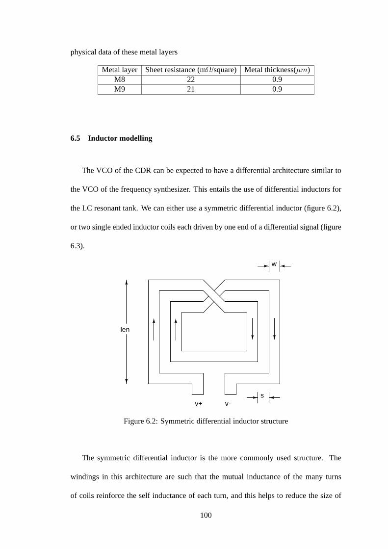
physical data of these metal layers
Metal layer Sheet resistance (mΩ/square) Metal thickness(µm)M8 22 0.9M9 21 0.9
6.5 Inductor modelling
The VCO of the CDR can be expected to have a differential architecture similar to
the VCO of the frequency synthesizer. This entails the use of differential inductors for
the LC resonant tank. We can either use a symmetric differential inductor (figure6.2),
or two single ended inductor coils each driven by one end of a differential signal (figure
6.3).
len
w
sv+ v-
Figure 6.2:Symmetric differential inductor structure
The symmetric differential inductor is the more commonly used structure. The
windings in this architecture are such that the mutual inductance of the many turns
of coils reinforce the self inductance of each turn, and this helps to reduce the size of
100
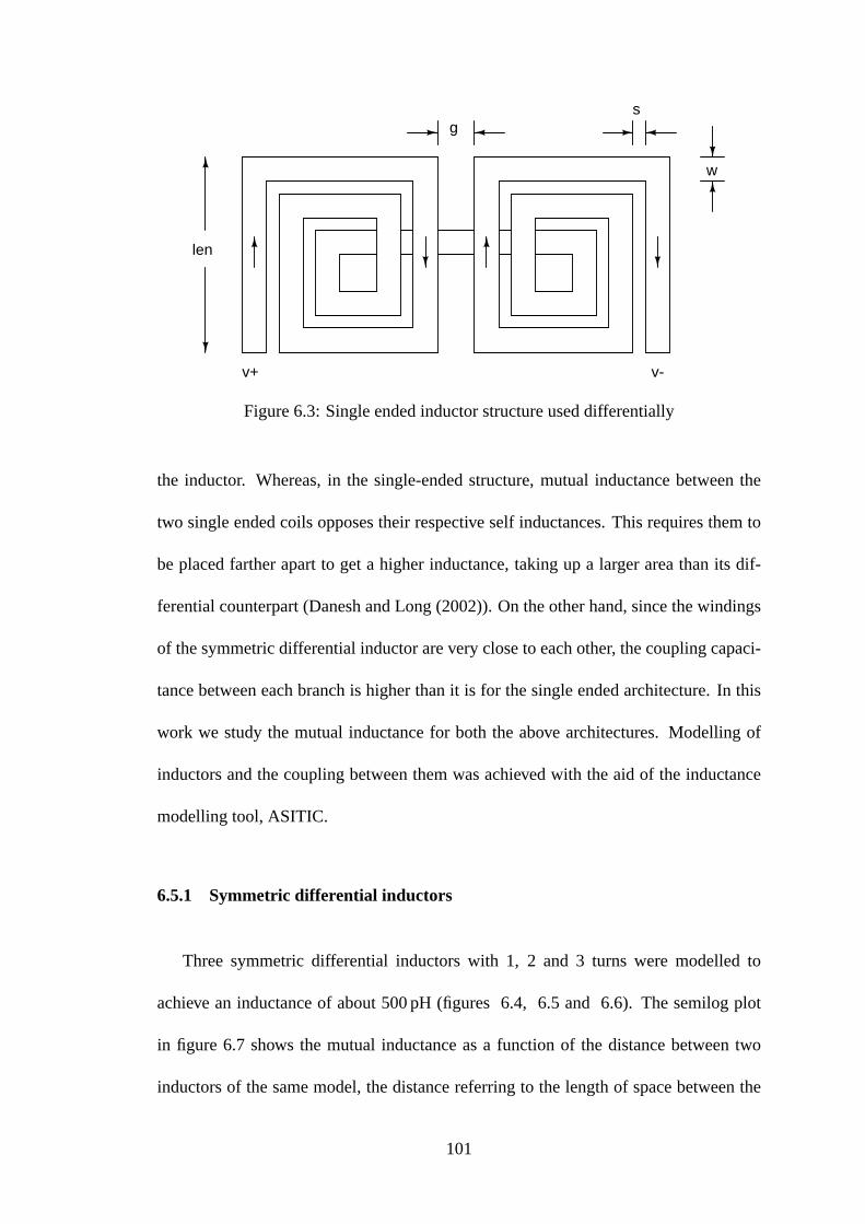
len
gs
w
v+ v-
Figure 6.3:Single ended inductor structure used differentially
the inductor. Whereas, in the single-ended structure, mutual inductance between the
two single ended coils opposes their respective self inductances. This requires them to
be placed farther apart to get a higher inductance, taking up a larger area than its dif-
ferential counterpart (Danesh and Long(2002)). On the other hand, since the windings
of the symmetric differential inductor are very close to each other, the coupling capaci-
tance between each branch is higher than it is for the single ended architecture. In this
work we study the mutual inductance for both the above architectures. Modelling of
inductors and the coupling between them was achieved with the aid of the inductance
modelling tool, ASITIC.
6.5.1 Symmetric differential inductors
Three symmetric differential inductors with 1, 2 and 3 turns were modelled to
achieve an inductance of about 500 pH (figures6.4, 6.5 and 6.6). The semilog plot
in figure 6.7 shows the mutual inductance as a function of the distance between two
inductors of the same model, the distance referring to the length of space between the
101

branches of the inductors closest to each other. The Q of the inductors were about 15. It
turns out that model III, which has the smallest area of the three, shows lower coupling
inductance, and the mutual coupling dips below 0.3 pH at less than300µm.
len=200µm
w=12µm
Figure 6.4:Symmetric differential inductor model I (n=1, L=478 pH)
v+ v-
w=13µm
s=3µm
len=120µm
Figure 6.5:Symmetric differential inductor model II (n=2, L=490 pH)
102

v+ v-
len=100µm
w=13µm
s=3µm
Figure 6.6:Symmetric differential inductor model III (n=3, L=475 pH)
100 200 300 400 500 60010
−2
10−1
100
101
Distance (µ m)
Mut
ual i
nduc
tanc
e (p
H)
Model IModel IIModel III
Figure 6.7:Plot of mutual coupling to distance for symmetric inductor models
103

6.5.2 Single ended inductors
Three models of single ended inductors was simulated using ASITIC, for three dif-
ferent orientations of each with respect to each other. The inductor models are seen in
figures 6.8, 6.9and 6.9, and the orientations relative to each other are seen in figures
6.11, 6.12and 6.13. The Q of the single-ended inductors were about 10. Figure6.14
shows a plot of the mutual inductance versus distance for the three models oriented at
0 to each other. Unlike in the case of symmetric square inductors, the mutual coupling
between the single-ended coils ebb very gradually with distance. This may make in-
tegration of two or more such inductors on a chip difficult. None of the curves in the
plot sinks below 0.3 pH even after600µm. Also, the single-ended inductor models I
and II exhibit a null in the inductive coupling at some distance characteristic of that
spiral, where the mutual coupling changes sign. This distance is usually very low, ly-
ing between100µm and200µm, which is too small for practical purposes. Even if it
were possible to place the CDR and the synthesizer so close to each other, if the null
predicted by simulation were slightly off from the actual null point, there is a risk of the
mutual inductance going beyond the desired value, since the coupling on either side of
the null changes steeply.
Figure 6.15 shows the mutual coupling between two single ended inductors of
model II for different orientations. It is seen that while the stacked configuration gives
the highest coupling, placing the inductors at90 degrees relative to each other mini-
mizes the coupling inductance. It is observed from simulation that the mutual induc-
tance reduces to below 0.3 pH beyond300µm when inductors of model II are oriented
at90 degrees relative to each other.
104

130µmw=15µm
d=70µm
v+ v-
130µm
Figure 6.8:Single ended inductor model I (n=1, L=600 pH)
130µm
w=15µm
d=20µm
v+ v-
130µm
Figure 6.9:Single ended inductor model II (n=1, L=550 pH)
105

l=70µm
10µm s=4µm
w=10µm
v+ v-
Figure 6.10:Single ended inductor model III (n=2.5, L=500 pH)
L1 L2
Oriented at 0o wrt each other
d
Figure 6.11:Inductor oriented at0 relative to the other
106

L1
L2
Oriented at 90o wrt each other
d
Figure 6.12:Inductor oriented at90 relative to the other
v+ v-
v+ v-
d
Figure 6.13:Inductor stacked over the other
107
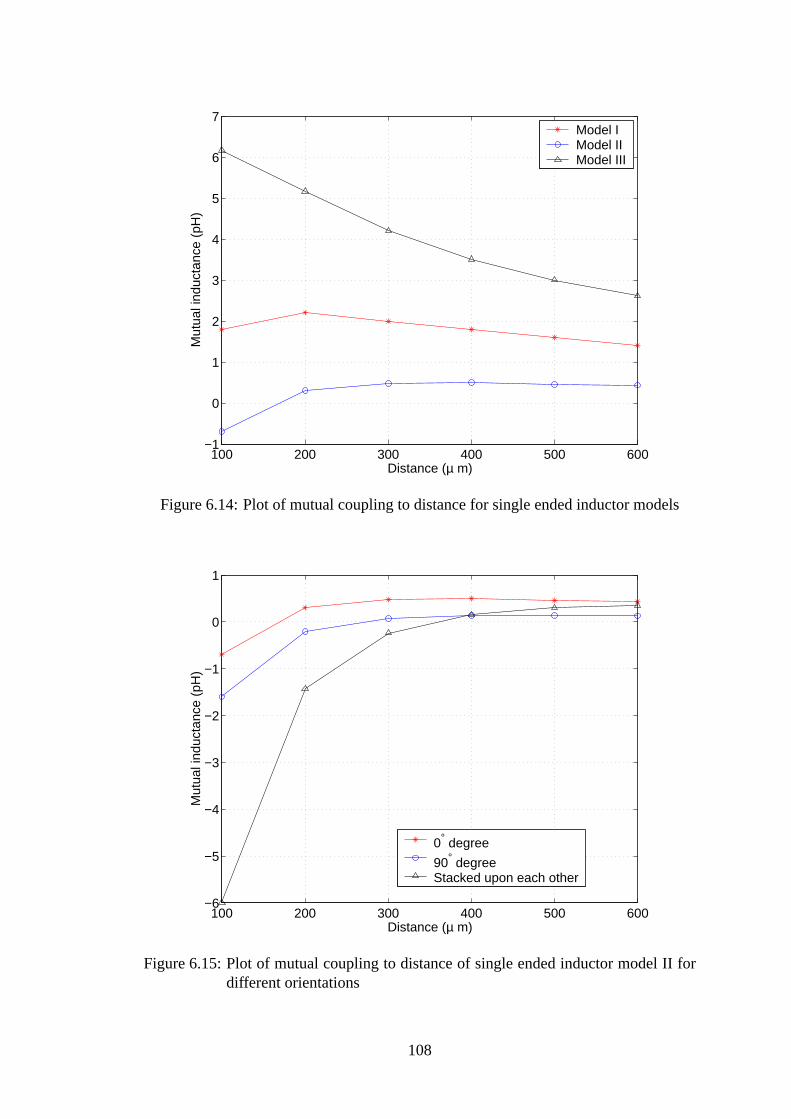
100 200 300 400 500 600−1
0
1
2
3
4
5
6
7
Distance (µ m)
Mut
ual i
nduc
tanc
e (p
H)
Model IModel IIModel III
Figure 6.14:Plot of mutual coupling to distance for single ended inductor models
100 200 300 400 500 600−6
−5
−4
−3
−2
−1
0
1
Distance (µ m)
Mut
ual i
nduc
tanc
e (p
H)
0° degree
90° degreeStacked upon each other
Figure 6.15:Plot of mutual coupling to distance of single ended inductor model II fordifferent orientations
108

6.6 Summary
The least coupling was exhibited by the symmetric differential inductor model III
seen in figure6.6, although the single-ended inductor model II of figure6.9 oriented
at 90 degrees also shows similar performance beyond300µm. But the single-ended
version suffers from a larger area and lesser Q than the symmetric differential induc-
tor mentioned and so the symmetric differential inductor model III would be the ideal
choice for the oscillators of the CDR and the frequency synthesizer.
109

CHAPTER 7
Summary
The frequency synthesizer, a 32x1 multiplexer and the feed-forward equalizer (FFE),
which are the blocks comprising the transmitter, have all been designed, while the
FFE has also been laid out. The frequency synthesizer has been designed to gener-
ate a 10 GHz clock with an rms jitter of less than a picosecond while dissipating about
10 mW of power. a 3-tap FFE has also been designed and laid-out and its total power
consumption is 42 mW. At the receiver end, the design of a clock and data recovery
circuit (CDR), based on a delay-locked loop (DLL) coupled to a phase-interpolator, has
been undertaken. The circuit is built for a frequency tolerance of±1000 ppm, and locks
to the incoming data in less than 200 ns. The power consumption of the CDR is about
30 mW. The multiplexer uses about 5 mW of power.
This work has also involved modeling on-chip inductors and to study the coupling
between inductors of two different architectures. It is observed that, for a given value of
inductance, symmetric differential inductors with a greater number of turns (and hence
lesser area) exert less influence on neighbouring spirals than single-ended inductor spi-
rals. This study can potentially be of use to a future endeavour to design a LC-VCO
based CDR placed on the same chip as the LC-VCO based frequency synthesizer.
All the blocks have been designed using TSMC 65nm CMOS technology. The
frequency synthesizer, the multiplexer and the CDR need to be laid-out and integrated
with the decision feedback equalizer (DFE) and variable gain amplifier (VGA) that have
been designed by my friend and colleague, Karthik T.J.

REFERENCES
1. Alexander, J. D. H. (1975). Clock Recovery from Random Binary Data.ElectronicLetters, 11, 541–542.
2. Bulzacchelli, J., M. Meghelli, S. Rylov, W. Rhee, A. Rylyakov, H. Ainspan,B. Parker, M. Beakes, A. Chung, T. Beukema, P. Pepeljugoski, L. Shan, Y. Kwark ,S. Gowda, andD. Friedman (2006). A 10-Gb/s 5-Tap DFE/4-Tap FFE Transceiver in90-nm CMOS Technology.IEEE Journal of Solid-State Circuits, 41(12), 2885–2900.
3. Danesh, M.andJ. R. Long (2002). Differentially Driven Symmetric Microstrip In-ductors.IEEE Transactions on Microwave Theory and Techniques, 50(1), 332–341.
4. Egan, W. F., Frequency Synthesis by Phase Lock. John Wiley & Sons, 1981.
5. Gardner, F. M., Phaselock Techniques. John Wiley & Sons, 2005, 3rd edition.
6. Hajimiri, A. andT. H. Lee (1998). A General Theory of Phase Noise in ElectricalOscillators.IEEE Journal of Solid-State Circuits, 33(2), 179–193.
7. Hanumolu, P. K., G.-Y. Wei, andU.-K. Moon (2008). A Wide-Tracking Range Clockand Data Recovery Circuit.IEEE Journal of Solid-State Circuits, 43(2), 425–439.
8. IEEE 802.3ap, 10GBASE-KR Backplane Ethernet Task Group. 2007.
9. Krishnapura, N. , M. Barazande-Pour, Q. Chaudhry, J. Khoury , K. Lakshmiku-mar, and A. Aggarwal, A 5Gb/s NRZ Transceiver with Adaptive Equalization forBackplane Transmission.In IEEE ISSCC Dig. Tech. Papers, San Francisco, CA. 2005.
10. Lee, H.-R., M.-S. Hwang, B.-J. Lee, Y.-D. Kim , D. Oh, J. Kim , S.-H. Lee, D.-K.Jeong, , andW. Kim (2005). A 1.2-V-Only 900-mW 10Gb Ethernet Transceiver andXAUI Interface With Robust VCO Tuning Technique.IEEE Journal of Solid-StateCircuits, 40(11), 2148–2158.
11. Lee, W.-H., J.-D. Cho, andS.-D. Lee, A high speed and low power Phase-FrequencyDetector and Charge-Pump.In Proceedings of the ASP-DAC ’99. Asia and South Pacificon Design Automation Conference, volume 1. 1999.
12. Magierowski, S., K. Iniewski , andS. Zukotynski, A Wideband LC-VCO with en-hanced PSRR for SoC Applications.In IEEE International Symposium on Circuits andSystems. 2004.
13. Mansuri, M. , D. Liu , andC. K. K. Yang (2002). Fast Frequency Acquisition Phase-Frequency Detectors for GSamples/s Phase-Locked Loops.IEEE Journal of Solid-StateCircuits, 37(10), 1331–1334.
14. Razavi, B.(2002). Challenges in the Design of High-Speed Clock and Data RecoveryCircuits. IEEE Communications Magazine.

15. Razavi, B., Design of Analog CMOS Integrated Circuits. Tata McGraw-Hill, 2002.
16. Razavi, B. (2004). A Study of Injection Locking and Pulling in Oscillators.IEEEJournal of Solid-State Circuits, 39(9), 1415–1424.
17. U. of California, Berkeley, ASITIC: Analysis and simulation of Spiral Inductors andTransformers for Integrated Circuits.
18. Walker, R. C., Phase-Locking in High-Performance Sytems - From Devices to Archi-tectures, chapter Designing Bang-bang PLLs for Clock and Data Recovery in SerialData Transmission Systems. IEEE Press, 2003, 34–45.
112