Embed Size (px)
Citation preview
DESIGN OF A 9 STAGE 10 BIT HIGH SPEED PIPELINE
ANALOG TO DIGITAL CONVERTER
by
Xi Long
A thesis submitted to the Faculty of the University of Delaware in partial fulfillment of the requirements for the degree of Master of Science in Electrical and Computer Engineering
Summer 2010
Copyright 2010 Xi Long All Rights Reserved

DESING OF A 9 STAGE 10 BIT HIGH SPEED PIPELINE
ANALOG TO DIGITAL CONVERTER
by
Xi Long
Approved: __________________________________________________________ Keith W. Goossen, Ph.D Professor in charge of thesis on behalf of the Advisory Committee Approved: __________________________________________________________ Kenneth E Barner, Ph.D Chair of the Department of Electrical and Computer Engineering Approved: __________________________________________________________ Michael J. Chajes, Ph.D Dean of the College of Engineering Approved: __________________________________________________________ Debra Hess Norris, M.S. Vice Provost for Graduate and Professional Education

iii
ACKNOWLEDGMENTS
First, I would like to thank my advisor, Dr. Keith G Goossen. I would not
have this opportunity without his kind help. Secondly, I would like to thank Dr. Fouad
Kiamilev for his guidance. My thanks also go to my colleagues and friends here at the
University of Delaware. Last but not the least, I thank my family for their kind support.
iv
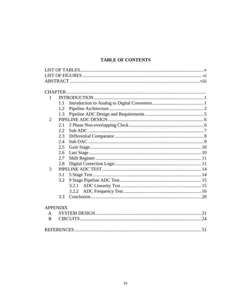
TABLE OF CONTENTS
LIST OF TABLES .......................................................................................................... v LIST OF FIGURES ....................................................................................................... vi ABSTRACT ................................................................................................................ viii CHAPTER ........................................................................................................................ 1 INTRODUCTION .............................................................................................. 1
1.1 Introduction to Analog to Digital Converters ............................................ 1 1.2 Pipeline Architecture ................................................................................. 2 1.3 Pipeline ADC Design and Requirements .................................................. 5
2 PIPELINE ADC DESIGN .................................................................................. 6 2.1 2 Phase Non-overlapping Clock ................................................................ 6 2.2 Sub ADC ................................................................................................... 7 2.3 Differential Comparator ............................................................................ 8 2.4 Sub DAC ................................................................................................... 9 2.5 Gain Stage................................................................................................ 10 2.6 Last Stage ................................................................................................ 10 2.7 Shift Register ........................................................................................... 11 2.8 Digital Correction Logic .......................................................................... 11
3 PIPELINE ADC TEST ..................................................................................... 14 3.1 5 Stage Test ............................................................................................. 14 3.2 9 Stage Pipeline ADC Test ...................................................................... 15
3.2.1 ADC Linearity Test ..................................................................... 15 3.2.2 ADC Frequency Test ................................................................... 16
3.3 Conclusion ............................................................................................... 20 APPENDIX A SYSTEM DESIGN ........................................................................................... 21 B CIRCUITS ........................................................................................................ 24 REFERENCES ............................................................................................................. 51

v
LIST OF TABLES
Table 1.1 Resolution and bandwidth tradeoffs .......................................................... 2
Table 3.1 Calculated output of 5 stage .................................................................... 15

vi
LIST OF FIGURES
Figure 1.1 Subranging of pipeline ADC .................................................................... 3
Figure 1.2 Pipeline ADC architecture ........................................................................ 4
Figure 1.3 Illustration of a pipeline stage .................................................................. 5
Figure 2.1 Sub ADC threshold and corresponding digital and residue output .......... 7
Figure 2.2 Concept of digital correction .................................................................. 12
Figure 2.3 Mathematics of digital correction ........................................................... 13
Figure 3.1 Linearity test of 9 stage ADC ................................................................. 16
Figure 3.2 Output digital code of 800KHz test ........................................................ 17
Figure 3.3 Spectrum of 800KHz test output ............................................................ 18
Figure 3.4 Output digital code of 7.2MHz test ........................................................ 19
Figure 3.5 Spectrum of 7.2MHz test output ............................................................ 20
Figure A.1 ADC diagram in Matlab Simulink ......................................................... 22
Figure A.2 Matlab simulation results of the 10 bit ADC ......................................... 23
Figure B.1 2 phase non-overlapping clock schematic .............................................. 25
Figure B.2 Simulation results of clock ..................................................................... 26
Figure B.3 Schematic of differential comparator ..................................................... 27
Figure B.4 Schematic of high speed comparator ...................................................... 28
Figure B.5 Test of high speed voltage comparator ................................................... 29
Figure B.6 Simulation results of high speed voltage comparator............................. 30
vii
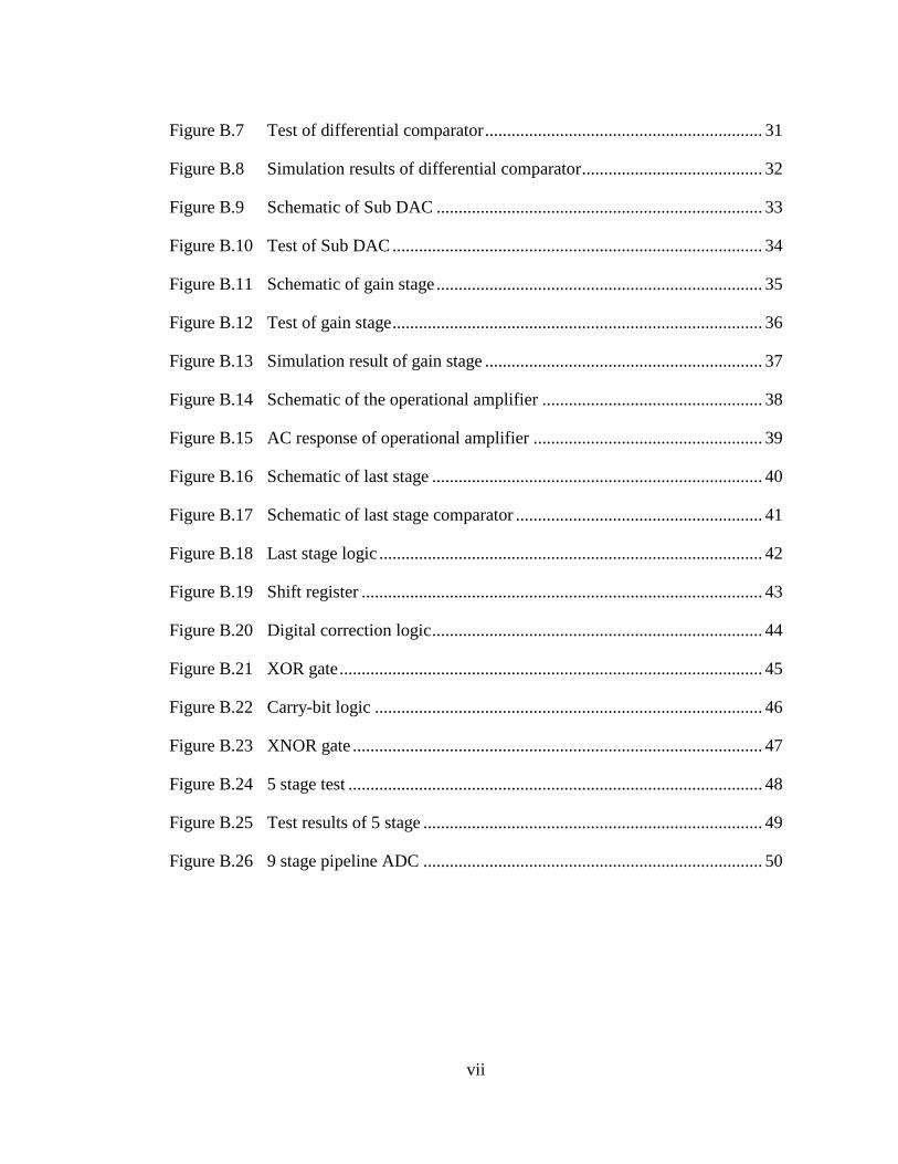
Figure B.7 Test of differential comparator ............................................................... 31
Figure B.8 Simulation results of differential comparator ......................................... 32
Figure B.9 Schematic of Sub DAC .......................................................................... 33
Figure B.10 Test of Sub DAC .................................................................................... 34
Figure B.11 Schematic of gain stage .......................................................................... 35
Figure B.12 Test of gain stage .................................................................................... 36
Figure B.13 Simulation result of gain stage ............................................................... 37
Figure B.14 Schematic of the operational amplifier .................................................. 38
Figure B.15 AC response of operational amplifier .................................................... 39
Figure B.16 Schematic of last stage ........................................................................... 40
Figure B.17 Schematic of last stage comparator ........................................................ 41
Figure B.18 Last stage logic ....................................................................................... 42
Figure B.19 Shift register ........................................................................................... 43
Figure B.20 Digital correction logic ........................................................................... 44
Figure B.21 XOR gate ................................................................................................ 45
Figure B.22 Carry-bit logic ........................................................................................ 46
Figure B.23 XNOR gate ............................................................................................. 47
Figure B.24 5 stage test .............................................................................................. 48
Figure B.25 Test results of 5 stage ............................................................................. 49
Figure B.26 9 stage pipeline ADC ............................................................................. 50

viii
ABSTRACT
Analog to digital converter (ADC) design has been an active research
topic over the past few decades, as the scaling down of Complementary Metal-Oxide-
Semiconductor (CMOS) Integrated Circuit (IC) fabrication process offers continuing
room for performance improvement. Various ADC architectures have been proposed
by researchers, including flash, successive approximation, sigma-delta and pipeline,
etc. Among these architectures, pipeline ADC offers moderate resolution at high
conversion speed and is widely used in both civil and military applications. In this
thesis, we develop a 9 stage 10 bit pipeline ADC circuit in AMIS C5N process. The
whole design methodology, from system simulation to schematic entry, from circuit
simulation to post signal analysis is proposed. The operation frequency of the pipeline
ADC is pushed to the upper limit of the process used. The ADC is designed and
simulated in Cadence environment. Post simulation signal analysis is done in Matlab
in order to verify its performance.
1
Chapter 1
INTRODUCTION
1.1 Introduction to Analog to Digital Converters
While virtually all processing of signals occurs in the digital domain
nowadays, the real world signals are analog. For example, the microphone inside a cell
phone picking up the sound of human voice generates a voltage whose amplitude may
vary from a few microvolts to hundreds of milivolts, while the photocells in a
camcorder produce a current on the scale of a few electrons per microsecond [1]. It is
desirable to convert these analog signals into digital form using an analog to digital
converter (ADC) for successive digital signal processing (DSP). Actually, some of the
intricate signal processing may only be feasible in the digital domain [2].
The design of ADCs for high speed, high precision and low power
dissipation has continuously been a challenge for analog designers. However, tradeoffs
always exist between these parameters. It is not uncommon that designers have to
sacrifice one for another. Basically, ADCs are divided into two categories: high speed
and high precision. Converters with a sampling rate greater than 10MHz are
considered high speed. Their application includes imaging, cameras, baseband
digitalization where the analog signal bandwidth is relatively broad. One of the issues
of high speed ADCs is their moderate resolution. Therefore in applications such as
high fidelity audio systems like CD player, high resolution ADCs are needed. The
2
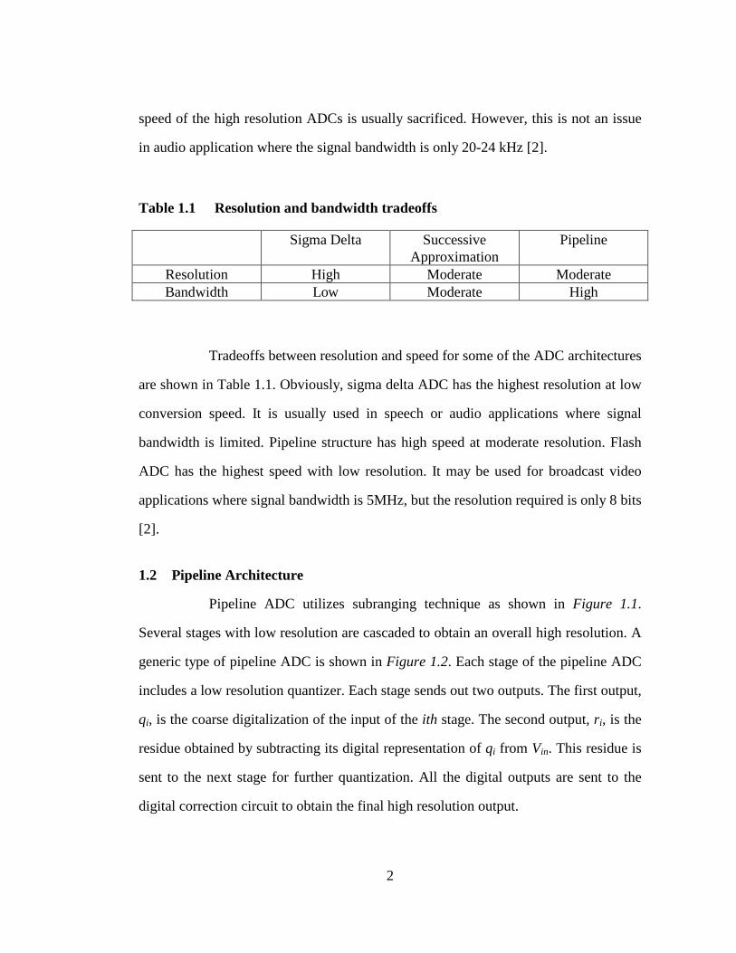
speed of the high resolution ADCs is usually sacrificed. However, this is not an issue
in audio application where the signal bandwidth is only 20-24 kHz [2].
Table 1.1 Resolution and bandwidth tradeoffs
Sigma Delta Successive Approximation
Pipeline
Resolution High Moderate Moderate Bandwidth Low Moderate High
Tradeoffs between resolution and speed for some of the ADC architectures
are shown in Table 1.1. Obviously, sigma delta ADC has the highest resolution at low
conversion speed. It is usually used in speech or audio applications where signal
bandwidth is limited. Pipeline structure has high speed at moderate resolution. Flash
ADC has the highest speed with low resolution. It may be used for broadcast video
applications where signal bandwidth is 5MHz, but the resolution required is only 8 bits
[2].
1.2 Pipeline Architecture
Pipeline ADC utilizes subranging technique as shown in Figure 1.1.
Several stages with low resolution are cascaded to obtain an overall high resolution. A
generic type of pipeline ADC is shown in Figure 1.2. Each stage of the pipeline ADC
includes a low resolution quantizer. Each stage sends out two outputs. The first output,
qi, is the coarse digitalization of the input of the ith stage. The second output, ri, is the
residue obtained by subtracting its digital representation of qi from Vin. This residue is
sent to the next stage for further quantization. All the digital outputs are sent to the
digital correction circuit to obtain the final high resolution output.

3
First Stage Second Stage
Figure 1.1 Subranging of pipeline ADC
A block diagram of a generic stage is shown in Figure 1.3. The input
signal is sampled by the sample and hold circuit. A sub ADC converts it into a coarse
digital output. The coarse digital output is then converted back into analog value by
the sub DAC. The analog value obtained is subtracted from Vin. The residue is
amplified and sent off to the next stage for further digitalization.

4
Stage 1 Stage 2 Stage N
Digital Correction Logic
Digital Output
Clock
Vin
q1 q2 qn
r1r2
Figure 1.2 Pipeline ADC architecture
Ideally, the resolution of the sub ADC can be just 1 bit. A simple
comparator would do the job. However, the comparator inside the sub ADC inevitably
suffers from threshold error. Input falling into that error range may not only cause an
error output bit at that specific stage, but also saturate the following stages. In order to
avoid ADC saturation, we introduce some digital redundancy in each stage by making
the sub ADC output more than 1 bit wide. It will be shown that the digital redundancy
introduced can correct the error bits caused by level shift of the comparator in the sub
ADC.

5
S/HVin
qi
Sub
ADC
Sub
DAC
+
-
ei Amplifierri
Figure 1.3 Illustration of a pipeline stage
1.3 Pipeline ADC Design and Requirements
In this paper, we propose to design a 9 stage 10 bit high speed analog to
digital converter circuit in AMIS C5N process. It operates at 5V power supply and
accepts -1 to 1 volts (2.5V common mode) fully differential input. The system design
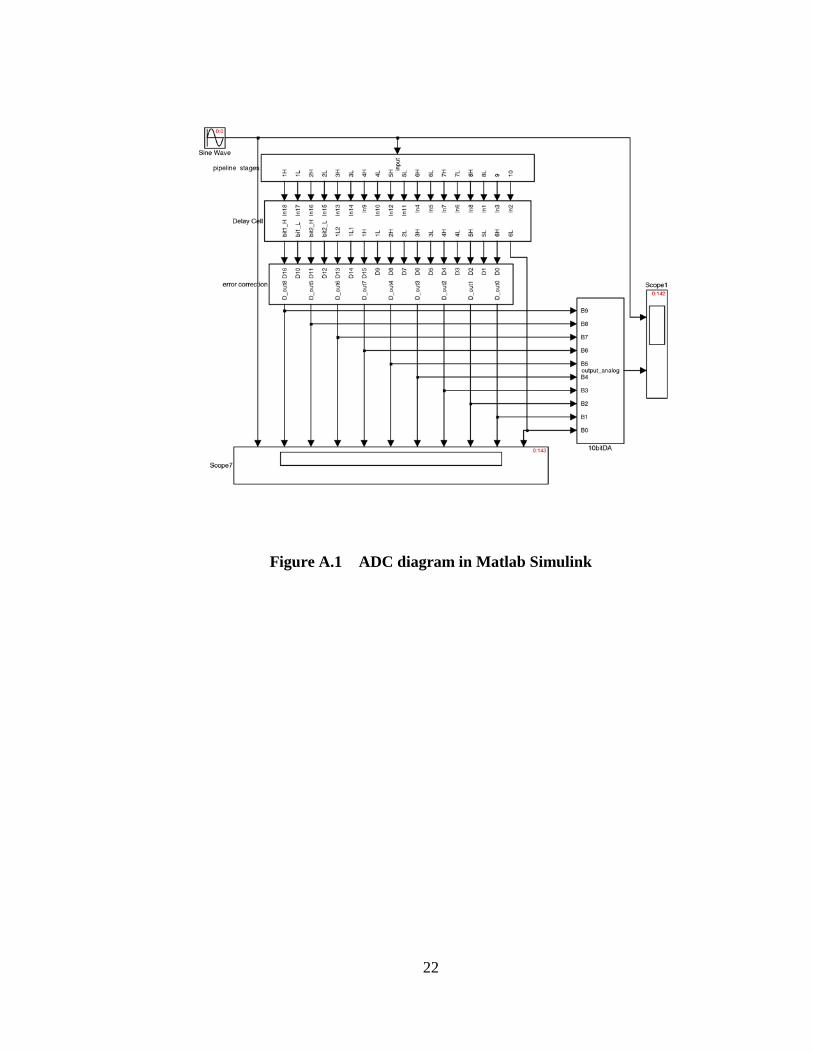
and simulation are done in Matlab, as shown in Appendix A.

6
Chapter 2
PIPELINE ADC DESIGN
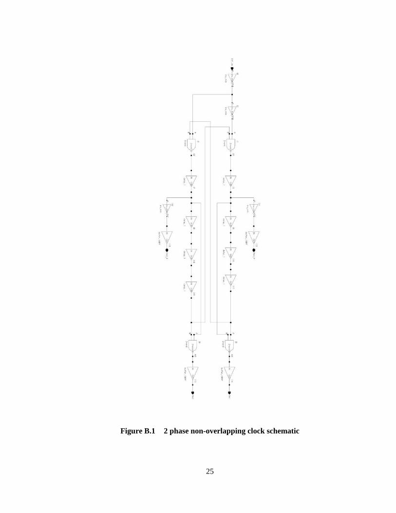
2.1 2 Phase Non-overlapping Clock
All stages operate on a two phase non-overlapping clock signal [3]. The
two clock signals, Ph1 and Ph2, are 180º out of phase and have a delay between the
clock transitions. All the odd stages sample the input during Ph1 and pass a valid
residue to the next stage during Ph2. The even stages work on the opposite timing
schedule. In this scheme, after an initial propagation delay, the ADC outputs valid bits
on every clock cycle.
Inside every stage there are switched capacitor circuits for sampling and
signal processing. In order to reduce the charge injection effect on the capacitors,
additional two clock signals Ph1’ and Ph2’ are introduced [1]. They are designed to
turn off slightly before Ph1 and Ph2, respectively.
The clock schematic is shown in Figure B.1. The design was adapted from
[3]. It utilizes delay elements and NAND gates to create the clock signals. The delay
elements consist of several inverters connected in series. All the output clock signals
are sent to a corresponding buffer to boost its driving capacity.
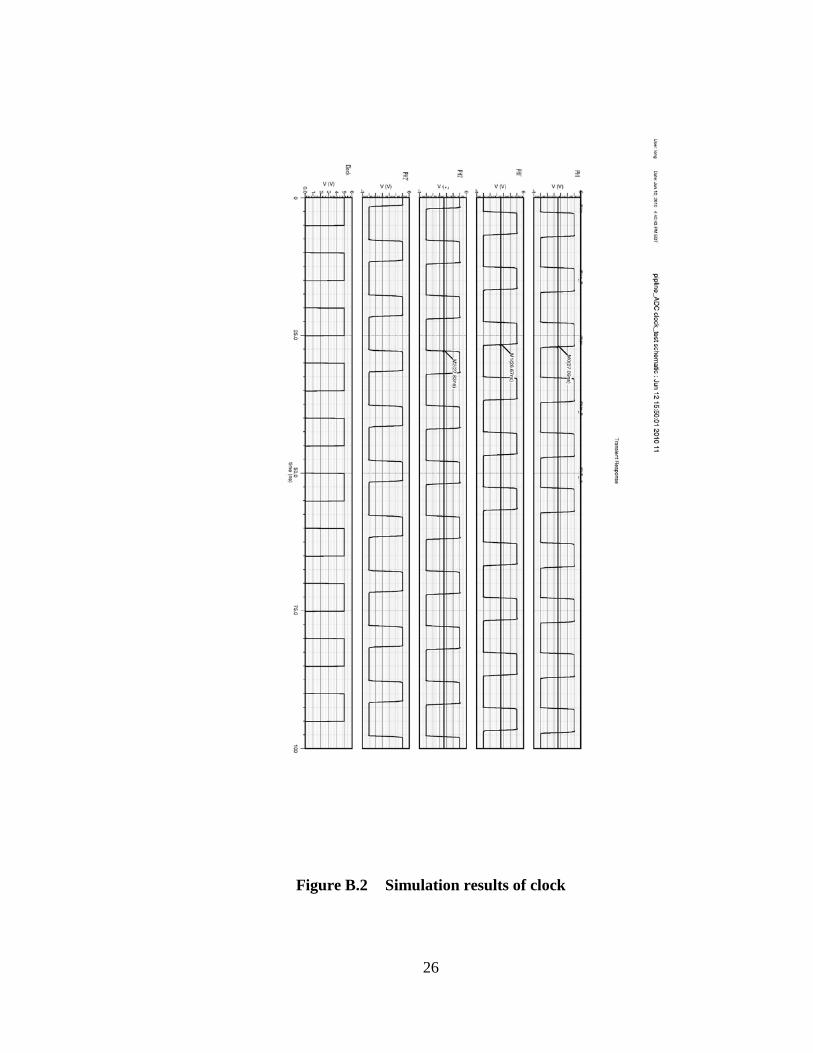
The two phase non overlapping clock is connected to a 100MHz clock
generator for test. The clock generator provides a square wave clock signal with
amplitude of 5V. The simulation result is show in Figure B.2.
7
It can be calculated from the Figure B.2 that tnov period, which is the non
overlapping period of Ph1 and Ph2, is about 0.7ns. The lagging period between Ph1 ad
Ph1’, tlag, is approximately 0.5ns. Therefore, each stage should settle in 3.8ns.
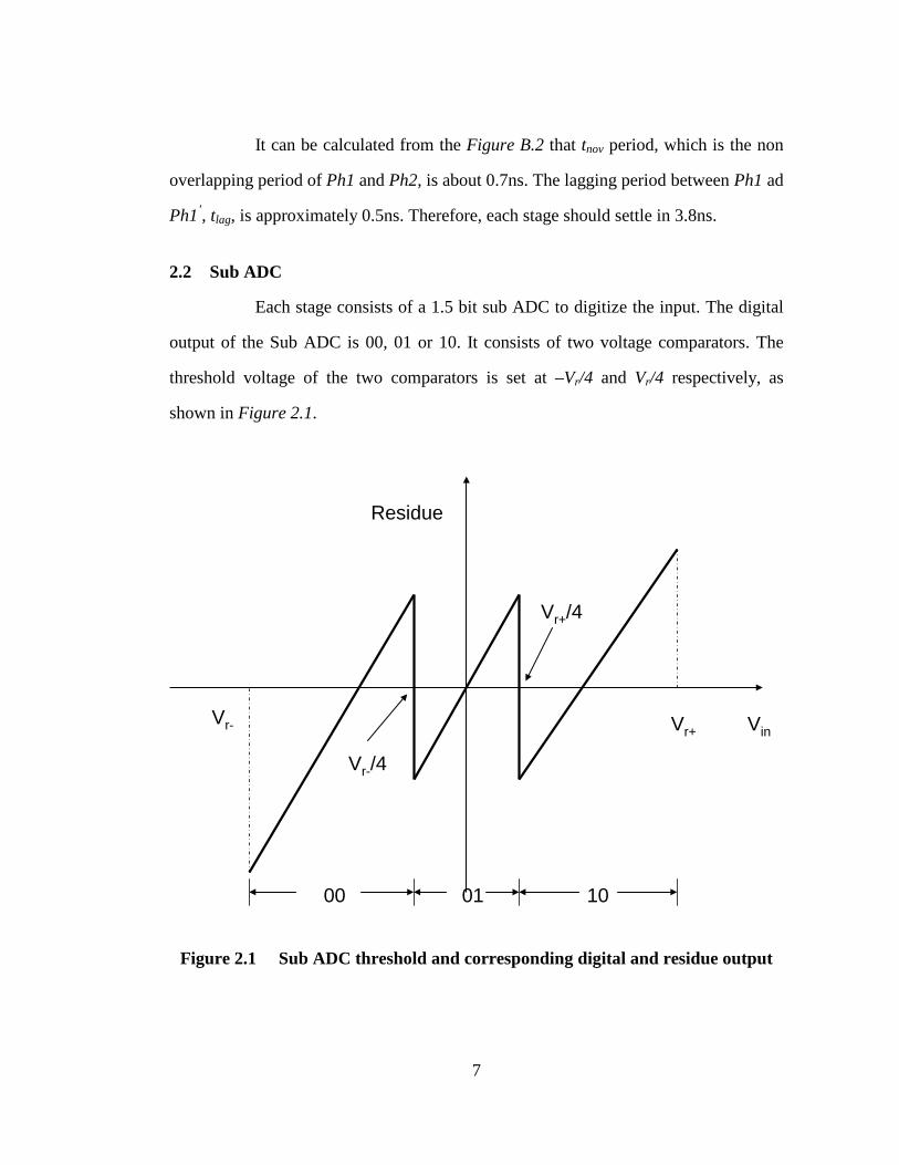
2.2 Sub ADC
Each stage consists of a 1.5 bit sub ADC to digitize the input. The digital
output of the Sub ADC is 00, 01 or 10. It consists of two voltage comparators. The
threshold voltage of the two comparators is set at –Vr/4 and Vr/4 respectively, as
shown in Figure 2.1.
Vr+Vr-
Residue
Vr-/4
Vr+/4
Vin
00 01 10
Figure 2.1 Sub ADC threshold and corresponding digital and residue output

8
There is great advantage of 1.5 bit sub ADC over 1 bit ADC. It is difficult
to precisely control the threshold voltage when designing a comparator. In 1.5 bit sub
ADC scheme, if the threshold voltage of the comparator deviates from the designed
value, it may cause wrong output bits in this stage. However, according to the above
figure, the residue output would not saturate, making it possible that the following
stages will correct this error.
2.3 Differential Comparator
The differential comparator consists of switching capacitor network and a
voltage comparator, as shown in Figure B.3. C0 and C3 sense the reference voltage
during Ph2. It passes partial of the stored charge to C1 and C2 during Ph1. The voltage
on C1 and C2 is subtracted from the input voltage and then sent to the voltage
comparator. The threshold of the differential comparator is set by the reference voltage.
When Vr+ is set to 3V and Vr- is set to 2V, the threshold voltage is 0.25V. When the
polarity of Vr+ and Vr- is switched, the threshold voltage becomes -0.25V.
The high speed comparator design is shown in Figure B.4. It consists of a
pre-amplification stage followed by a decision and a buffer stage. The output is latched
when the latch_bar signal is high. The output is pre-charged to high to improve the
response time on high output. The comparator is found to be the most critical part of
the design. When pushing it up to high speed operation, it is difficult to maintain
precision comparison [4].
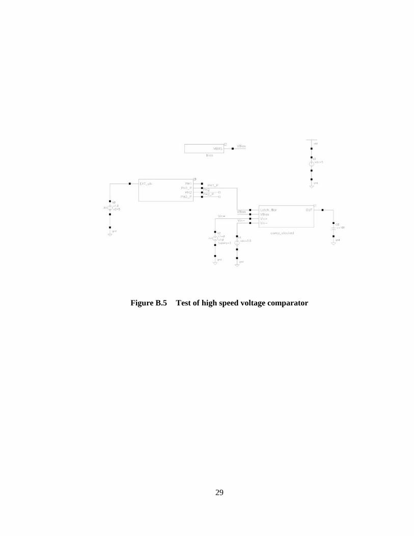
The high speed voltage comparator is tested in configuration illustrated in
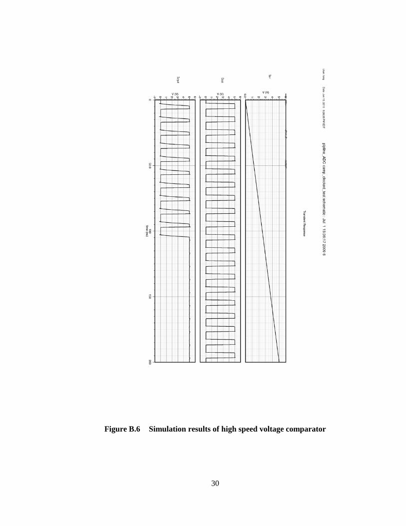
Figure B.5. Vin- is connected to a 2.5V DC source, while Vin+ is ramped from 0 to 3V.

9
The simulation is done at 100MHz. The simulation results in Figure B.6 show that the
comparator works well at 100 MHz clock frequency.
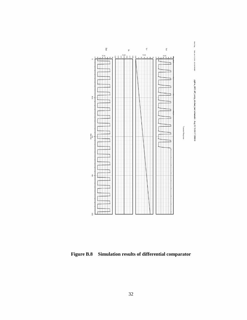
The differential comparator will follow the characteristics of the voltage
comparator. The test details are omitted here. Please refer to Appendix B to see test
setup and corresponding results.
2.4 Sub DAC
The sub DAC is used to convert the quantized output of the sub ADC into
analog value. The analog output of the sub DAC is sent to the gain stage to be
subtracted from the input signal to form the residue, which is sent out to the next stage
for further quantization. The sub DAC also outputs digital bits to the shift register and
correction logic. In the 1.5 bit scheme, the digital outputs are 00, 01, 10. The
corresponding DAC analog outputs are -Vr/2, 0, Vr/2. The residue of the gain stage
has to be multiplied by a factor of 2 before being sent to the next stage. In order to
alleviate the complexity of the gain stage design, the output of sub DAC is amplified
by a factor of 2 before the subtraction operation. In other words, the analog output of
the sub DAC is -Vr, 0, Vr.
The detailed design of the sub DAC is shown in Figure B.9. The
combination logic consisting of inverters and 3NAND gates generates the digital bits
and control signal for the transmission gates. NMOS transistors are used for the
transmission gates to pass –Vr and Vr to the analog outputs.
Similar scheme is used to simulate the sub ADC as the differential
comparator, as shown in Figure 10. Two comparators are used to provide full range
digitalization. The simulation is done at 100MHz. The simulation results show that the
designed sub DAC works well at 100 MHz.
10
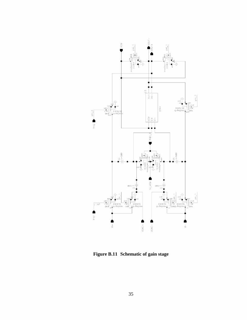
2.5 Gain Stage
The gain stage is used to subtract the output of the sub DAC from the
input and pass the residue to the next stage. The schematic of the gain stage is shown
in Figure B.11. The OTA block in the schematic is an operational amplifier. During
Ph1, Vin charges the four capacitors: C2, C3, C4, C5. At Ph2, C4 and C5 are
reconnected to the output of the OTA while C2 and C3 are connected to the residual
voltage from the previous stage. This causes the charge on C2 and C3 to change. The
charge variance is transferred to C4 and C5. The final output voltage at the differential
outputs is equal to 2Vi – Vdac, which can be conveniently calculated based on
previous analysis.
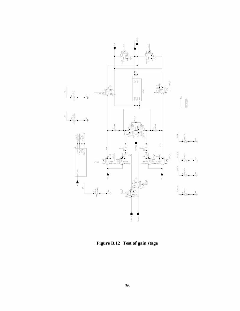
The gain stage is tested in configuration shown in Figure B.12. Vdac+ is
set to be 3V, Vdac- is set to be 2.5V. Vin is set to be 0.2V in the first 1us and -0.2V in
the second 1us. The clock frequency is set to be 50MHz. The simulation result is
shown in Figure B.13. The output voltage is -0.1V and -0.9V, which agrees with
theoretical calculation.
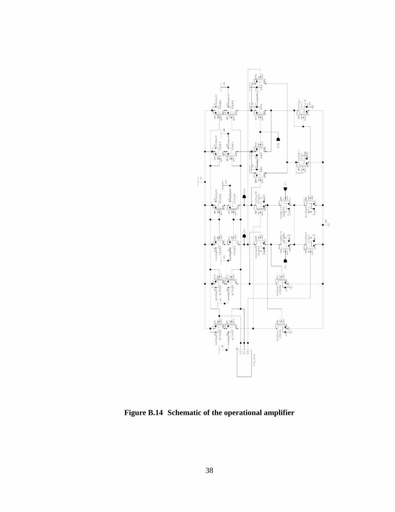
The schematic of the transconductance operational amplifier is shown in
Figure B.14. It is a single stage differential amplifier adapted from [5]. In order to
boost its gain, cascaded telescopic structure is used. It also consists of a gain boosting
stage to further increse the gain and a common mode feedback circuit to regulate the
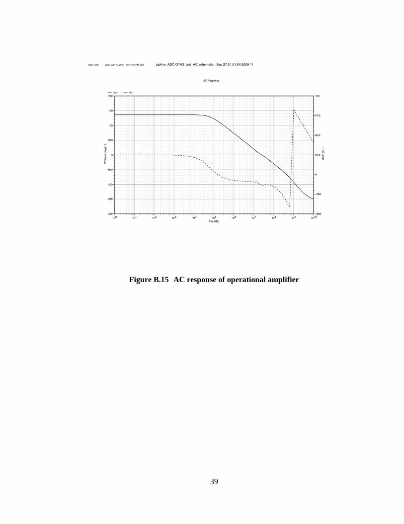
common mode output voltage. The AC simulation response is shown in Figure B.15.
It shows it has a 75dB DC gain and a phase margin of 45 degree.
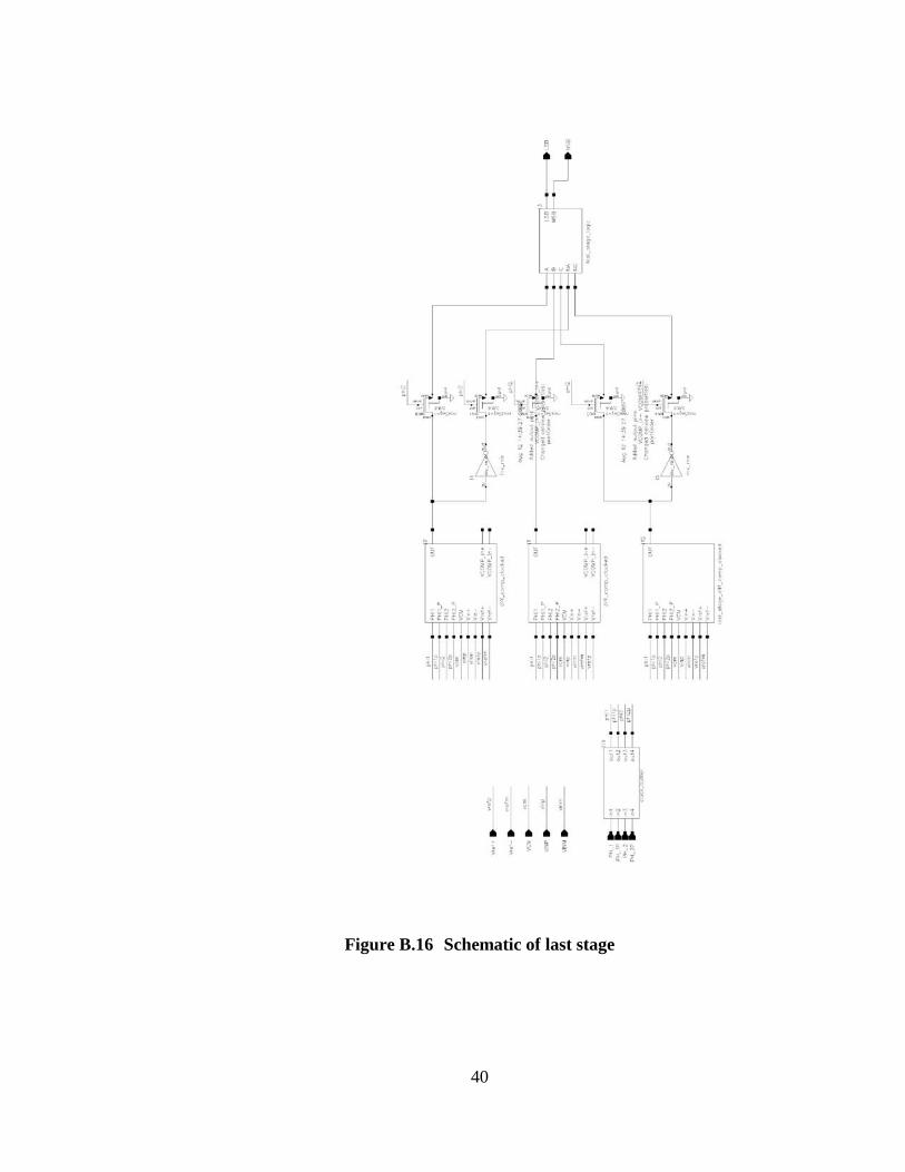
2.6 Last Stage
The last stage has similar structure as the other stages. However, the last
stage does not generate the residual voltage so the gain stage is eliminated. Secondly,

11
the last stage has a full 2 bit output capacity. The sub ADC and sub DAC design are
modified accordingly. A third comparator is added to the sub ADC. The threshold
voltage is set to be Vr/2 by changing the value of the corresponding switching
capacitors. The DAC does not need to output any analog residual, so the transmission
gates are eliminated. The logic is modified to output a full 2 bit signal: 00, 01, 10 and
11. The schematic of the last stage and its sub components are shown in Appendix B.
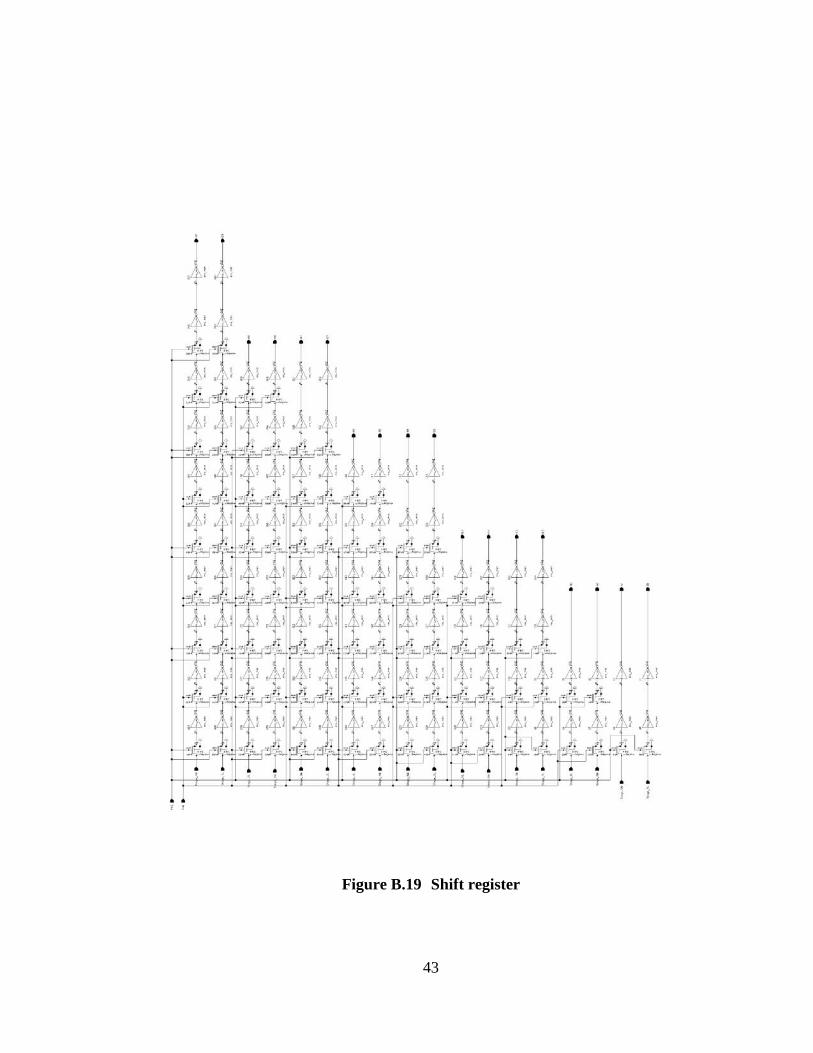
2.7 Shift Register
The shift register as shown in Figure B.19 is used to store the intermediate
output bits from the sub DAC. For a 9 stage pipeline ADC, the output bits of the
previous 8 stages must be stored in the register before output bits of the last stage
become available. The shift register consists of minimum sized inverter connected
with MOS switches. All odd stages have outputs available at Ph1, while all even
stages have outputs available at Ph2. The outputs propagate in the shift register. The
delay is determined by the length of the shift register. After an initial delay, the shift
register array has new outputs available at each clock cycle. The outputs of the shift
register array are sent to the digital correction logic for successive processing.
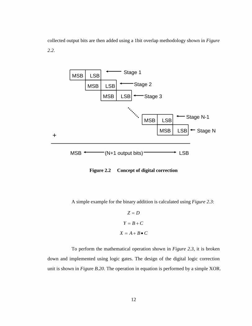
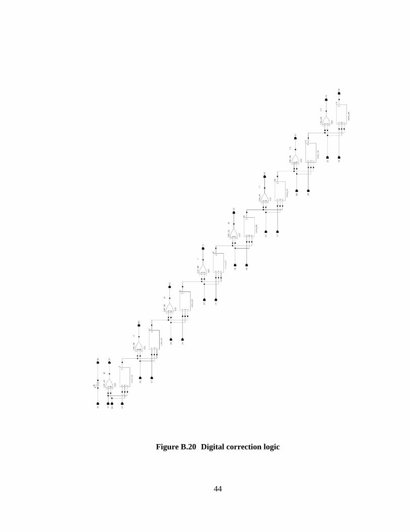
2.8 Digital Correction Logic
The output of the shift register is sent to the digital correction logic. In
pipeline ADC, digital redundancy is utilized to compensate sub ADC errors. As a
result, twice as many bits are generated than required for the output. A digital
correction logic is required to produce the correct output. The concept of the correction
logic is represented in Figure 2.2, which is adapted from [4]. The outputs of the
previous stages are stored in the register until stage N has its output available. The
12
collected output bits are then added using a 1bit overlap methodology shown in Figure
2.2.
MSB LSB
MSB LSB
MSB LSB
MSB LSB
MSB LSB
Stage 1
Stage 2
Stage 3
Stage N-1
Stage N+
MSB LSB(N+1 output bits)
Figure 2.2 Concept of digital correction
A simple example for the binary addition is calculated using Figure 2.3:
DZ =
CBY +=
CBAX •+=
To perform the mathematical operation shown in Figure 2.3, it is broken
down and implemented using logic gates. The design of the digital logic correction
unit is shown in Figure B.20. The operation in equation is performed by a simple XOR.

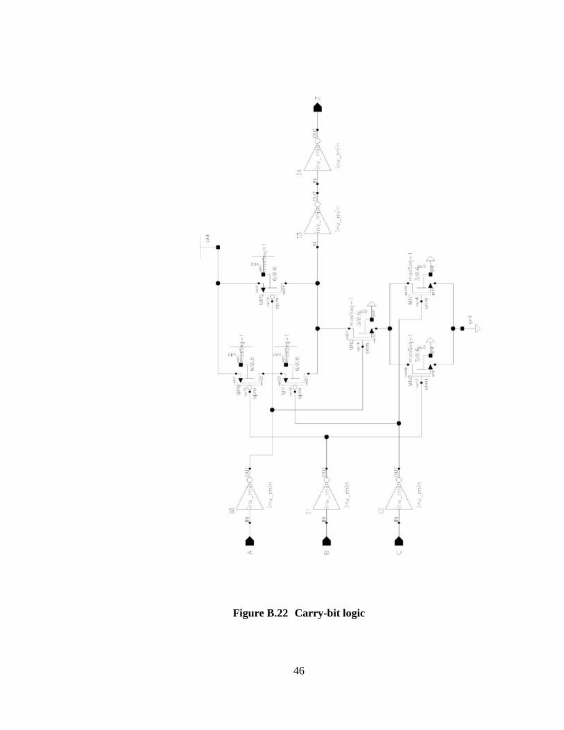
13
The CARRY-BIT logic performs the AND/OR operation in equation. These logic
gates are shown in appendix B.
A B
C D+
X Y Z
Figure 2.3 Mathematics of digital correction

14
Chapter 3
PIPELINE ADC TEST
3.1 5 Stage Test
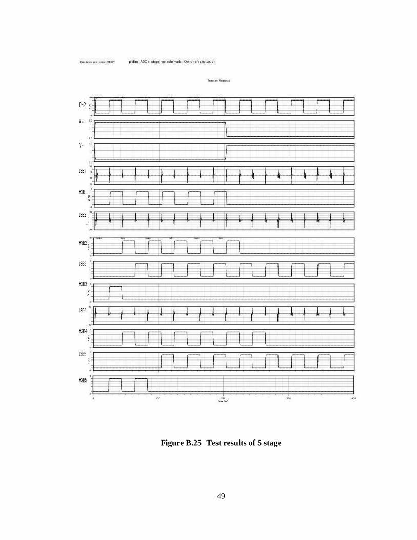
5 stages are cascaded to test the functionality of the circuit components, as
shown in Figure B.24. The clock frequency is set to be 25MHz. Vr+ and Vr- are set to
be 3V and 2V respectively. The 5 stage configuration is simulated for 400 ns. The
differential input switches from 0.8V in the first 200ns to -0.8V in the last 200ns. The
intermediate bits and sub DAC analog output of each stage are calculated and shown
in Table 3.1. The duplicate value results from the possible threshold variation in
comparators that is taken into consideration. The simulation result is shown in Figure
B.25. The simulation performed at 25MHz clock frequency shows the 5 stage ADC
works properly. Simulations are also done at higher frequency. It turns out the
performance of the ADC downgrades as the frequency increases, causing error output
bits. The upper bound frequency is found to be around 40MHz.

15
Table 3.1 Calculated output of 5 stage
Vdiff Intermediate bits Sub DAC output 0.8 10 0.6 0.6 10 0.2 0.2 10
01 -0.6 0.4
-0.2 01 00
-0.4 -0.6
-0.8 00 -0.6 -0.6 00 -0.2 0.6 -0.4
10 00
0.2 0.2
0.2 10 01
-0.6 0.4
3.2 9 Stage Pipeline ADC Test
The 9 stages, shift register and the correction logic are assembled to form
the pipeline ADC, as shown in Figure B.26. The pipeline ADC is tested under two
configurations. In the first configuration, the input voltage is ramped from -1V to 1V.
The outputs are converted to normalized digital codes. The digital codes are compared
with the input to show the linearity of the ADC. In the second configuration, sine
wave of different frequency is fed into the ADC. Spectrum analysis of the output is
performed to characterize the pipeline ADC under test.
3.2.1 ADC Linearity Test
In the linearity test, the input is ramped from -1V to 1V. The outputs of
the ADC are collected in 0.2V interval from the Cadence Spectre simulation output.
The data are then fed into Matlab for analysis. The clock frequency is set at 25 MHz.
The test result is shown in Figure 3.1. It shows the linearity of the ADC agrees with an

16
ideal ADC. INL and DNL can be obtained from the test results. However, it is not
performed here due to time constraints.
Figure 3.1 Linearity test of 9 stage ADC
3.2.2 ADC Frequency Test
The pipeline ADC is tested under different input frequencies to evaluate
its performance. 64 data points are collected at the output. The operating frequency is
set to 25.6 MHz. Two tests of different frequency are performed here. The low test
frequency is set to 800KHz, while the high test frequency is set to 7.2 MHz. The
output spectrum is analyzed by FFT in Matlab. The 800KHz test output digital code is
shown in Figure 3.2. A clear sine wave can be seen here. The corresponding FFT
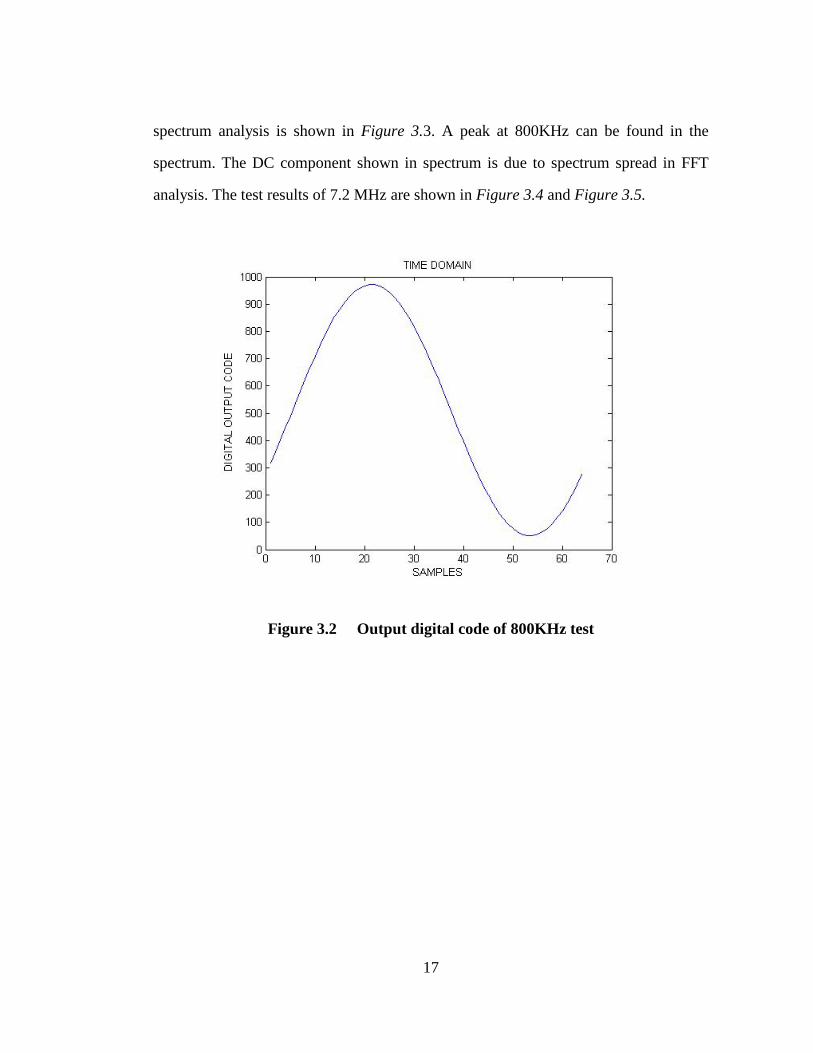
17
spectrum analysis is shown in Figure 3.3. A peak at 800KHz can be found in the
spectrum. The DC component shown in spectrum is due to spectrum spread in FFT
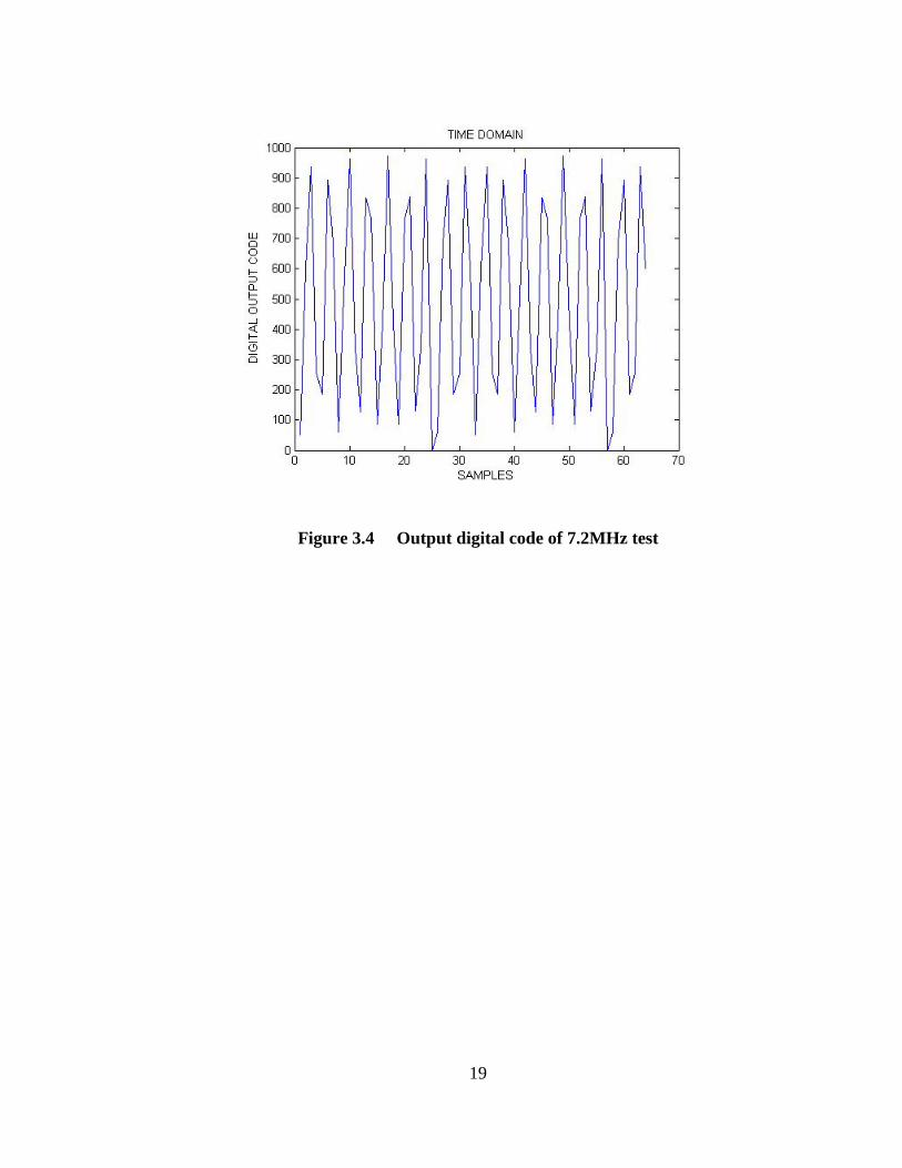
analysis. The test results of 7.2 MHz are shown in Figure 3.4 and Figure 3.5.
Figure 3.2 Output digital code of 800KHz test

18
Figure 3.3 Spectrum of 800KHz test output
19
Figure 3.4 Output digital code of 7.2MHz test

20
Figure 3.5 Spectrum of 7.2MHz test output
3.3 Conclusion
The objective of this project is to design a 10 bit 9 stage high speed analog
to digital converter. It operates on 5V power supply and accepts -1 to 1 volts (2.5V
common mode offset voltage) fully differential input. All of the objectives have been
accomplished. The ADC exhibits good linearity and works at sampling rate up to
40MHz. The simulation is performed at the schematic level. Full layout of the chip is
not done due to time constraints. Further work involves transistor level layout,
physical extraction and pushing the sampling rate to higher frequency.

21
Appendix A
SYSTEM DESIGN
22
Figure A.1 ADC diagram in Matlab Simulink
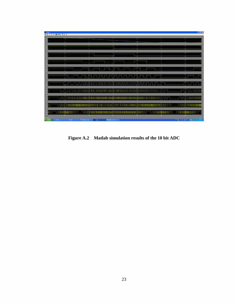
23
Figure A.2 Matlab simulation results of the 10 bit ADC

24
Appendix B
CIRCUITS
25
Figure B.1 2 phase non-overlapping clock schematic
26
Figure B.2 Simulation results of clock

27
Figure B.3 Schematic of differential comparator

28
Figure B.4 Schematic of high speed comparator
29
Figure B.5 Test of high speed voltage comparator
30
Figure B.6 Simulation results of high speed voltage comparator

31
Figure B.7 Test of differential comparator
32
Figure B.8 Simulation results of differential comparator

33
Figure B.9 Schematic of Sub DAC

34
Figure B.10 Test of Sub DAC
35
Figure B.11 Schematic of gain stage
36
Figure B.12 Test of gain stage

37
Figure B.13 Simulation result of gain stage
38
Figure B.14 Schematic of the operational amplifier
39
Figure B.15 AC response of operational amplifier
40
Figure B.16 Schematic of last stage

41
Figure B.17 Schematic of last stage comparator

42
Figure B.18 Last stage logic
43
Figure B.19 Shift register
44
Figure B.20 Digital correction logic

45
Figure B.21 XOR gate
46
Figure B.22 Carry-bit logic
47
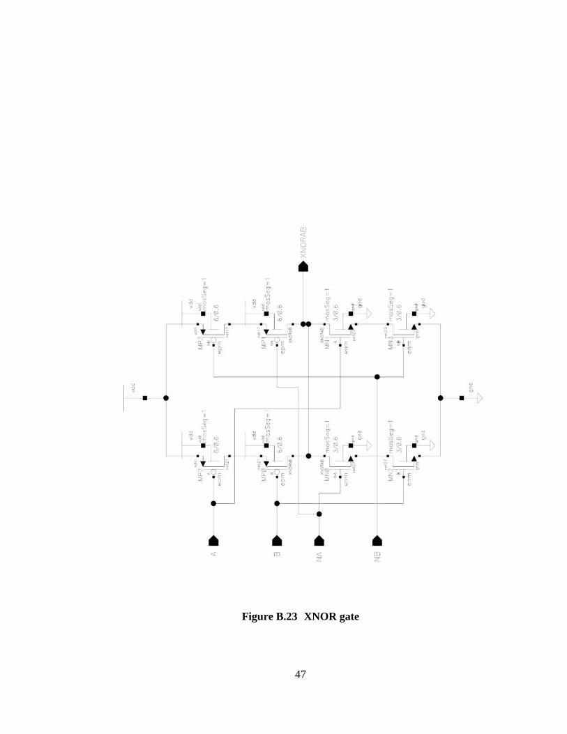
Figure B.23 XNOR gate

48
Figure B.24 5 stage test
49
Figure B.25 Test results of 5 stage

50
Figure B.26 9 stage pipeline ADC
51
REFERENCES
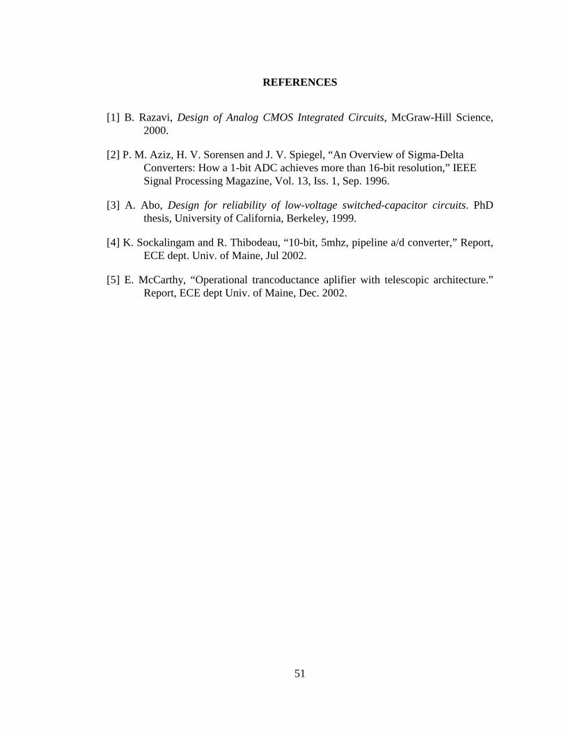
[1] B. Razavi, Design of Analog CMOS Integrated Circuits, McGraw-Hill Science, 2000.
[2] P. M. Aziz, H. V. Sorensen and J. V. Spiegel, “An Overview of Sigma-Delta Converters: How a 1-bit ADC achieves more than 16-bit resolution,” IEEE Signal Processing Magazine, Vol. 13, Iss. 1, Sep. 1996.
[3] A. Abo, Design for reliability of low-voltage switched-capacitor circuits. PhD thesis, University of California, Berkeley, 1999.
[4] K. Sockalingam and R. Thibodeau, “10-bit, 5mhz, pipeline a/d converter,” Report, ECE dept. Univ. of Maine, Jul 2002.
[5] E. McCarthy, “Operational trancoductance aplifier with telescopic architecture.” Report, ECE dept Univ. of Maine, Dec. 2002.