Embed Size (px)
Citation preview
A masters thesis
Department of Industrial Electrical Engineering and Automation
Lund Institute of Technology
Design Of A Current ControlledDefibrillator
ByMagnus Jonsson, e99Filip Jörgensen, e99
Supervised by:Per Karlsson

AbstractThis report describes the design procedures and underlying theory needed in or-der to engineer a current controlled defibrillator. Electric circuits are presentedand explained together with the theory for some of the more important com-ponents like the transformer and the IGBT. The need for protective circuitryregarding overvoltage is investigated and safety issues are discussed.
The high voltage is achieved by using a flyback converter to charge a capac-itor. This capacitor is discharged via an H-bridge and the current is controlledusing a hardware tolerance band controller. Three types of discharge are avail-able, monophasic, biphasic and triphasic.
The entire system is controlled by an ATMega8 processor monitoring thecharging and creating the necessary PWM.

AknowledgementDuring this masters thesis much help has been recieved from several people andcompanies. The following is an alphabetical list of the people and companieswe would like to thank.
• Mats Alaküla, professor at the department of industrial electrical engineer-ing and automation, LTH
• Coilcraft, manufacturer of coils and transformers, supplying us with freesamples
• Getaschew Darge, engineer and technichian at the department of industrialelectronics and automation, LTH
• Fairchild semiconductors, manufacturer of semiconductors, supplying uswith free samples
• Eilert Johansson, engineer at Profec AB, manufacturer of custom madetransformers
• Per Karlsson, our supervisor at the department of industrial electricalengineering and automation, LTH
• Maxim IC, manufacturer of semiconductors, supplying us with free sam-ples
• Audrius Paskevicius, our supervisor at Xenodenice AB
• Johan Åkesson, tech. lic. at the department of automatic control provid-ing us with knowledge of discrete digital controllers.
Contents
1 Introduction 1
2 Scope and purpose 2
3 Defibrillators and LUCAS 33.1 Different types of defibrillators . . . . . . . . . . . . . . . . . . . 33.2 The defibrillator in LUCAS . . . . . . . . . . . . . . . . . . . . . 4
3.2.1 Energy efficiency . . . . . . . . . . . . . . . . . . . . . . . 43.2.2 Weight, size and cost . . . . . . . . . . . . . . . . . . . . . 43.2.3 Variable variables . . . . . . . . . . . . . . . . . . . . . . . 5
4 Voltage transformation 64.1 Energy and voltage levels . . . . . . . . . . . . . . . . . . . . . . 64.2 The IGBT and the MOSFET . . . . . . . . . . . . . . . . . . . . 64.3 Converter topologies . . . . . . . . . . . . . . . . . . . . . . . . . 74.4 The flyback converter . . . . . . . . . . . . . . . . . . . . . . . . 7
4.4.1 Primary side of the flyback converter . . . . . . . . . . . . 74.4.2 The transformer . . . . . . . . . . . . . . . . . . . . . . . 104.4.3 Secondary side of the flyback converter . . . . . . . . . . 13
4.5 Controlling the charging . . . . . . . . . . . . . . . . . . . . . . . 154.6 Safety . . . . . . . . . . . . . . . . . . . . . . . . . . . . . . . . . 19
4.6.1 Automatic discharge . . . . . . . . . . . . . . . . . . . . . 194.6.2 Over voltage shutdown . . . . . . . . . . . . . . . . . . . . 21
5 Discharge 255.1 The four quadrant converter . . . . . . . . . . . . . . . . . . . . . 255.2 Controlling the discharge . . . . . . . . . . . . . . . . . . . . . . 26
6 Software 326.1 ATMega8 . . . . . . . . . . . . . . . . . . . . . . . . . . . . . . . 326.2 Overview . . . . . . . . . . . . . . . . . . . . . . . . . . . . . . . 336.3 Menu system . . . . . . . . . . . . . . . . . . . . . . . . . . . . . 34
6.3.1 Charge voltage . . . . . . . . . . . . . . . . . . . . . . . . 346.3.2 Discharge type . . . . . . . . . . . . . . . . . . . . . . . . 346.3.3 Current control . . . . . . . . . . . . . . . . . . . . . . . . 346.3.4 Phase length . . . . . . . . . . . . . . . . . . . . . . . . . 346.3.5 Safety time . . . . . . . . . . . . . . . . . . . . . . . . . . 346.3.6 Idle time . . . . . . . . . . . . . . . . . . . . . . . . . . . 346.3.7 Discharge current . . . . . . . . . . . . . . . . . . . . . . . 356.3.8 User banks . . . . . . . . . . . . . . . . . . . . . . . . . . 35
6.4 Defibrillation system . . . . . . . . . . . . . . . . . . . . . . . . . 35
7 Result 377.1 Charging . . . . . . . . . . . . . . . . . . . . . . . . . . . . . . . 377.2 Discharging and current control . . . . . . . . . . . . . . . . . . . 387.3 Meeting the standards . . . . . . . . . . . . . . . . . . . . . . . . 417.4 Future improvements . . . . . . . . . . . . . . . . . . . . . . . . . 41
IV

A Technical specifications iA.1 Ports . . . . . . . . . . . . . . . . . . . . . . . . . . . . . . . . . . iA.2 Buttons . . . . . . . . . . . . . . . . . . . . . . . . . . . . . . . . iA.3 Current consumption . . . . . . . . . . . . . . . . . . . . . . . . . i
B Hardware iiB.1 Discharging plots . . . . . . . . . . . . . . . . . . . . . . . . . . . ii
B.1.1 No current control . . . . . . . . . . . . . . . . . . . . . . iiB.1.2 Current control . . . . . . . . . . . . . . . . . . . . . . . . iii
B.2 Charging . . . . . . . . . . . . . . . . . . . . . . . . . . . . . . . vB.2.1 Schematic . . . . . . . . . . . . . . . . . . . . . . . . . . . vB.2.2 PCB . . . . . . . . . . . . . . . . . . . . . . . . . . . . . . vi
B.3 Discharge . . . . . . . . . . . . . . . . . . . . . . . . . . . . . . . viiB.3.1 Schematic . . . . . . . . . . . . . . . . . . . . . . . . . . . viiB.3.2 PCB . . . . . . . . . . . . . . . . . . . . . . . . . . . . . . viii
B.4 ATMega8 and control . . . . . . . . . . . . . . . . . . . . . . . . ixB.4.1 Schematic . . . . . . . . . . . . . . . . . . . . . . . . . . . ixB.4.2 PCB . . . . . . . . . . . . . . . . . . . . . . . . . . . . . . x
C Software xiC.1 Graphical User Interface . . . . . . . . . . . . . . . . . . . . . . . xiC.2 Program listing . . . . . . . . . . . . . . . . . . . . . . . . . . . . xii
V
Page 1 of 43 Design of a Current Controlled Defibrillator
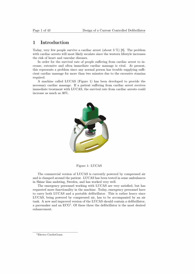
1 IntroductionToday, very few people survive a cardiac arrest (about 3 %) [8]. The problemwith cardiac arrests will most likely escalate since the western lifestyle increasesthe risk of heart and vascular diseases.
In order for the survival rate of people suffering from cardiac arrest to in-crease, extensive and often immediate cardiac massage is vital. At present,this represents a problem since any normal person has trouble supplying suffi-cient cardiac massage for more than two minutes due to the excessive staminarequired.
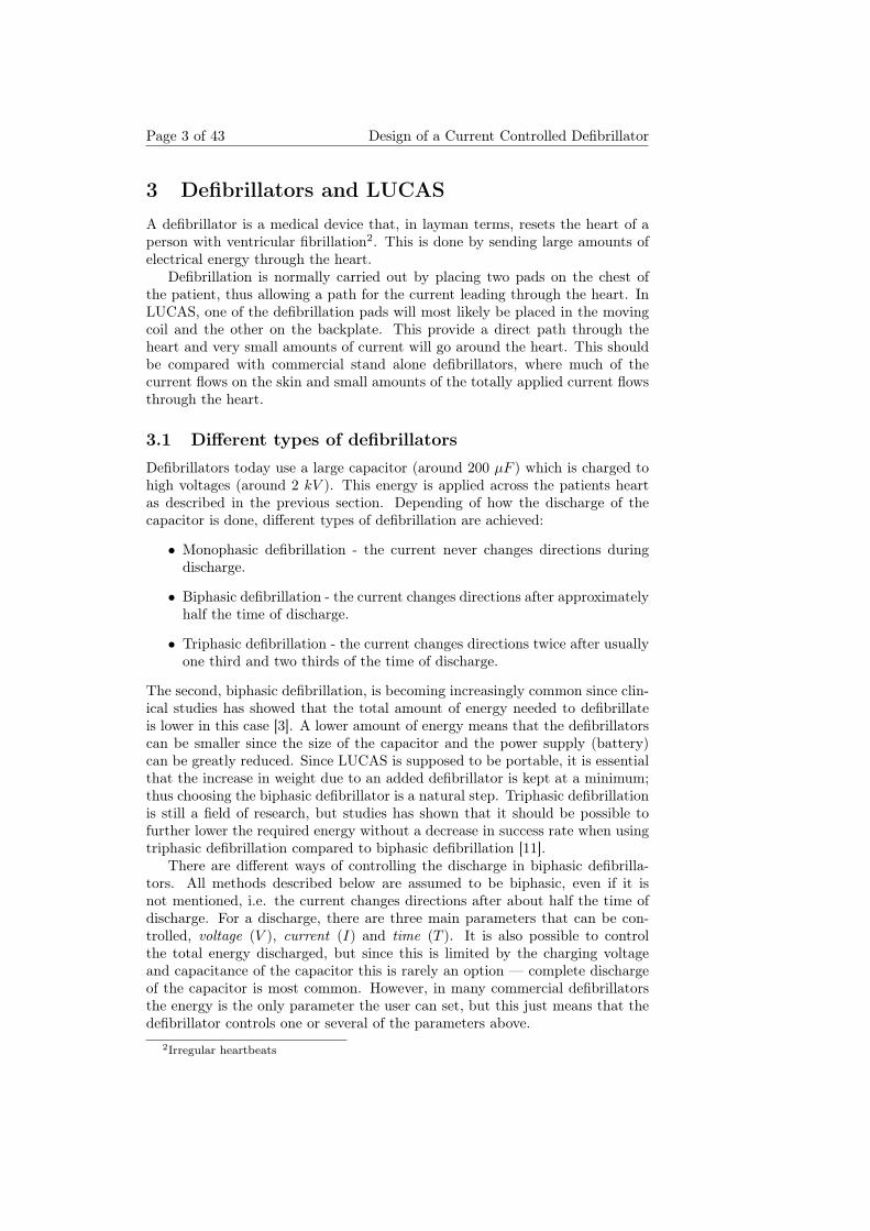
A machine called LUCAS (Figure 1) has been developed to provide thenecessary cardiac massage. If a patient suffering from cardiac arrest receivesimmediate treatment with LUCAS, the survival rate from cardiac arrests couldincrease as much as 30%.
Figure 1: LUCAS
The commercial version of LUCAS is currently powered by compressed airand is clamped around the patient. LUCAS has been tested in some ambulancesin Skåne läns andsting, Sweden, and has worked very well.
The emergency personnel working with LUCAS are very satisfied, but hasrequested more functionality in the machine. Today, emergency personnel haveto carry both LUCAS and a portable defibrillator. This is rather heavy sinceLUCAS, being powered by compressed air, has to be accompanied by an airtank. A new and improved version of the LUCAS should contain a defibrillator,a pacemaker and an ECG1. Of these three the defibrillator is the most desiredenhancement.
1Electro CardioGram
Section 2 Page 2 of 43
2 Scope and purposeThe purpose of this master thesis is to investigate the possibility of integrating afully functional medical defibrillator into LUCAS. As previously described thisis a requested functionality from a user point of view and therefore an importantstep forward in the development process for LUCAS.
There are a number of activities that has been conducted in order to reachthe desired goal. First of all, there are a number of medical requirements thathas to be taken into account. These requirements are not carved into stone sincethis is an area of intensive development and discussions on how to achieve thebest clinical results. This leads to the fact that the defibrillation unit initiallyhas to have an extensive set of adjustable parameters. These parameters willlater be fixed when elaborative tests show what settings seems to give the bestresults.
The next step is to investigate component selection and different circuitlayouts that will meet the maximum ratings for the previously defined require-ments. This is a difficult area since cost, weight and electrical specifications hasto be taken into account. Simulations and calculations are needed to determinewhich solutions that are feasible.
A coarse schematics has been developed and a number of prototype boardshave been built. These prototypes serve as a guide to which theoretical presump-tions that meet specifications and which have to be reworked. After thoroughtests in a power laboratory the prototype is now ready for some clinical tests.At this point medical expertise is required in order to evaluate acquired results.
If the results are satisfactory the development process moves forward to adifferent route which unfortunately is out of the scope for this master thesis.This route includes cost and weight reduction, medical certification, furtherclinical studies among other things.
Page 3 of 43 Design of a Current Controlled Defibrillator
3 Defibrillators and LUCASA defibrillator is a medical device that, in layman terms, resets the heart of aperson with ventricular fibrillation2. This is done by sending large amounts ofelectrical energy through the heart.
Defibrillation is normally carried out by placing two pads on the chest ofthe patient, thus allowing a path for the current leading through the heart. InLUCAS, one of the defibrillation pads will most likely be placed in the movingcoil and the other on the backplate. This provide a direct path through theheart and very small amounts of current will go around the heart. This shouldbe compared with commercial stand alone defibrillators, where much of thecurrent flows on the skin and small amounts of the totally applied current flowsthrough the heart.
3.1 Different types of defibrillatorsDefibrillators today use a large capacitor (around 200 µF ) which is charged tohigh voltages (around 2 kV ). This energy is applied across the patients heartas described in the previous section. Depending of how the discharge of thecapacitor is done, different types of defibrillation are achieved:
• Monophasic defibrillation - the current never changes directions duringdischarge.
• Biphasic defibrillation - the current changes directions after approximatelyhalf the time of discharge.
• Triphasic defibrillation - the current changes directions twice after usuallyone third and two thirds of the time of discharge.
The second, biphasic defibrillation, is becoming increasingly common since clin-ical studies has showed that the total amount of energy needed to defibrillateis lower in this case [3]. A lower amount of energy means that the defibrillatorscan be smaller since the size of the capacitor and the power supply (battery)can be greatly reduced. Since LUCAS is supposed to be portable, it is essentialthat the increase in weight due to an added defibrillator is kept at a minimum;thus choosing the biphasic defibrillator is a natural step. Triphasic defibrillationis still a field of research, but studies has shown that it should be possible tofurther lower the required energy without a decrease in success rate when usingtriphasic defibrillation compared to biphasic defibrillation [11].
There are different ways of controlling the discharge in biphasic defibrilla-tors. All methods described below are assumed to be biphasic, even if it isnot mentioned, i.e. the current changes directions after about half the time ofdischarge. For a discharge, there are three main parameters that can be con-trolled, voltage (V ), current (I) and time (T ). It is also possible to controlthe total energy discharged, but since this is limited by the charging voltageand capacitance of the capacitor this is rarely an option — complete dischargeof the capacitor is most common. However, in many commercial defibrillatorsthe energy is the only parameter the user can set, but this just means that thedefibrillator controls one or several of the parameters above.
2Irregular heartbeats
Section 3 Page 4 of 43
The easiest way to control the defibrillation is to control the time. This isdone by simply charging the capacitor to the desired voltage and then discharg-ing it directly through the patient creating an RC-circuit with its characteristicdischarging behavior. One problem with this method is that the resistance ofthe patient has to be measured prior to defibrillation, however this is not a ma-jor problem since most defibrillators usually have some kind of protection fromshort circuit and open air discharge which means that measuring the resistanceprior to defibrillation in most cases is a must. The major problem is instead thehigh current at the start of the defibrillation since high currents might result inburn-marks on the patient.
Voltage controlled defibrillation is not considered a good idea. If the volt-age was to be controlled, one has to charge the capacitor to a voltage muchhigher than the one desired in the discharge since the voltage delivered from thecapacitor will decrease as the discharge commences. This could be solved byconstantly charging the capacitor from the power source, but this would resultin a transformer that is capable of delivering large amounts of current on thesecondary side which in turn would render the capacitance obsolete leaving thedefibrillator very large and heavy due to the overly dimensioned transformerand power source.
Current controlled defibrillation is becoming increasingly common. The cur-rent is allowed to swing between preset values and if the amount of energystored in the capacitor is sufficient, both phases of the biphasic defibrillationcan be made current controlled. Current controlled defibrillation is an areaunder research and is believed to be the future choice.[9]
3.2 The defibrillator in LUCAS
The defibrillator to be placed in LUCAS has to be very energy efficient and hasto have low weight, small size and low cost. Factors like ease of use and thepossibility to alter currents, voltages and discharge times has to be considered.
3.2.1 Energy efficiency
The energy efficiency of the defibrillator is essential since this will reduce thesize of the required battery. With low energy efficiency it is likely that powerdissipation in the device will cause the device to heat up and overly dimensionedheat sinks might be needed.
The entire design of the LUCAS defibrillator need to be imbued with energyefficient thoughts. The switching losses need to be kept at a minimum andgreat care has to be taken regarding energy consumption when choosing thecomponents.
3.2.2 Weight, size and cost
As mentioned, the weight of LUCAS must not be significantly increased by theintegration of a defibrillator. This means that the final product must be opti-mized when it comes to weight and size. However, the weight issue is somewhatout of the scope of this masters thesis since the battery and capacitor are themain contributers to the increased weight.
Page 5 of 43 Design of a Current Controlled Defibrillator
The size of the defibrillator can, and should, be optimized as early as possiblein the design process. This is accomplished by minimizing the footprint3 of thedefibrillator. Components need to be chosen as small as possible and a tightschematic layout is of great importance. However, at this stage, trade-offs haveto be considered, small and tight components are (usually) more expensive thanlarger ones and a certain amount of common sense need be used in order tooptimize size/cost. Additionally, the voltage level is rather high so isolationdistances need to be considered in order to achieve reliable and safe operation.
3.2.3 Variable variables
Since the concept of defibrillation through the human body (chest to back) isnot as well documented as normal defibrillation (chest to chest) much researchis needed before a suitable configuration can be found. This means that thedischarging and charging options should be maximized. The defibrillator inLUCAS should be a biphasic defibrillator, but should it be possible to defibrillatewith monophasic and triphasic waveforms? Current controlled defibrillationshould be considered, but how much current is needed when defibrillation isperformed through the body? These parameters and many more need to beinvestigated before the device is taken into production. For this reason theoutcome of this masters thesis need to be a prototype providing freedom to setthese variables so that medical personnel can perform clinical tests and decidethe features of the final product.
The possibility to vary the following parameters should be considered in aprototype:
• Monophasic-/biphasic-/triphasic defibrillation
• Discharge current/-voltage
• Current control on/off
• Time of discharge
• Idle time4
3Size on PCB4Time between the positive and negative defibrillation pulse
Section 4 Page 6 of 43
4 Voltage transformation
4.1 Energy and voltage levels
A crucial part of the defibrillating system is that a high voltage source is needed.Since LUCAS is a portable unit, the highest voltage available is 12 volts from thebuilt-in battery. This voltage level is not sufficient to drive any larger currentsinto the human body since clinical measurements show that 95% of the humanpopulation have a body resistance in the range of 30 to 90 Ω [9].
Hence, the idea is to use a transforming circuit boosting the battery voltageto a defined voltage level which is then stored in a high voltage capacitor. Thecapacitor, which acts like a fuel tank during the defibrillation sequence, has astored energy level which can be calculated using the formula
W =C · U2
2Joule (1)
In many commercial defibrillation systems the energy level is the predom-inant, and sometimes the only setting, that the user can alter. These energylevels are usually predefined in the range of 200 to 360 Joule. In order to storethis kind of energy, the market for high voltage capacitors was investigated.There are a few capacitors that are specifically intended for use in defibrillationsystems, and a capacitor with the electrical characteristics 196 µF and 3 kVwas selected. If a maximum energy level of 360 Joule is desired, the capacitorsmaximum voltage should at least exceed 1.9 kV according to (1).
Creating this voltage is possible, but care has to be taken that the compo-nents of the charging and discharging circuits can cope with such high voltagelevels.
4.2 The IGBT and the MOSFET
High power switching applications has not always been easy to perform withouthigh losses in switching. Until recently, (1980’s) BJT’s5 where used since theyhave lower power dissipation compared with the faster MOSFET6. In 1984 [6]the IGBT7 was introduced combining the best of two worlds. The IGBT hasthe fast switching of the MOSFET and the lower on state losses of the BJT.The IGBT allows high current, high voltage switching with low losses.
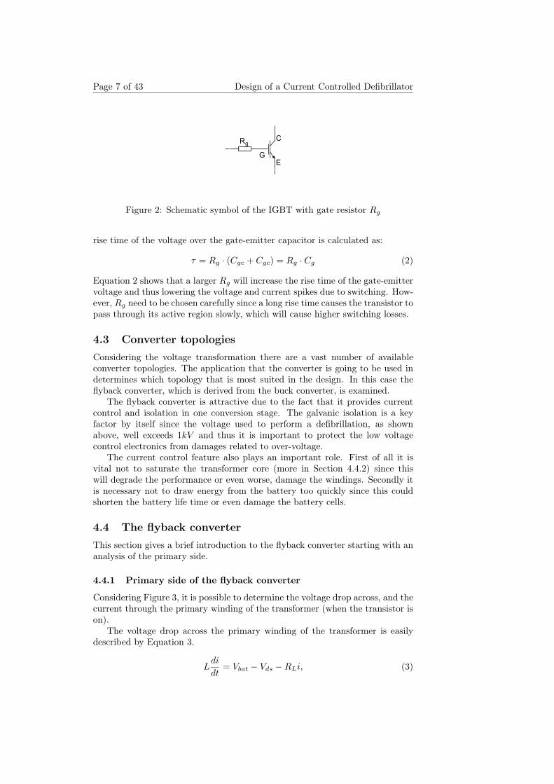
The IGBT, just like the MOSFET, is voltage controlled, i.e. there is acapacitive coupling between the gate and the emitter (Cge) and between gateand collector (Cgc) of the transistor. The total gate capacitance is the sum ofCgc and Cge and will hereafter be refered to as the gate capacitance Cg. Thismeans that the switching time is proportional to the equivalent capacitance ofthe gate (Cg = Cgc + Cgc) and the resistance connected to the gate (RG). Theschematic symbol of the IGBT is shown in Figure 2 [10].
Since high speed switching may cause voltage and current spikes throughthe transistor the feature with Rg is very useful. The same problem with spikesarise when the transistor is turned off, which is solved by the same resistor. The
5Bipolar Junction Transistor6Metal Oxide Semi Conductor7Insulated Gate Bipolar Transistor
Page 7 of 43 Design of a Current Controlled Defibrillator
Rg
GE
C
Figure 2: Schematic symbol of the IGBT with gate resistor Rg
rise time of the voltage over the gate-emitter capacitor is calculated as:
τ = Rg · (Cgc + Cgc) = Rg · Cg (2)
Equation 2 shows that a larger Rg will increase the rise time of the gate-emittervoltage and thus lowering the voltage and current spikes due to switching. How-ever, Rg need to be chosen carefully since a long rise time causes the transistor topass through its active region slowly, which will cause higher switching losses.
4.3 Converter topologiesConsidering the voltage transformation there are a vast number of availableconverter topologies. The application that the converter is going to be used indetermines which topology that is most suited in the design. In this case theflyback converter, which is derived from the buck converter, is examined.
The flyback converter is attractive due to the fact that it provides currentcontrol and isolation in one conversion stage. The galvanic isolation is a keyfactor by itself since the voltage used to perform a defibrillation, as shownabove, well exceeds 1kV and thus it is important to protect the low voltagecontrol electronics from damages related to over-voltage.
The current control feature also plays an important role. First of all it isvital not to saturate the transformer core (more in Section 4.4.2) since thiswill degrade the performance or even worse, damage the windings. Secondly itis necessary not to draw energy from the battery too quickly since this couldshorten the battery life time or even damage the battery cells.
4.4 The flyback converterThis section gives a brief introduction to the flyback converter starting with ananalysis of the primary side.
4.4.1 Primary side of the flyback converter
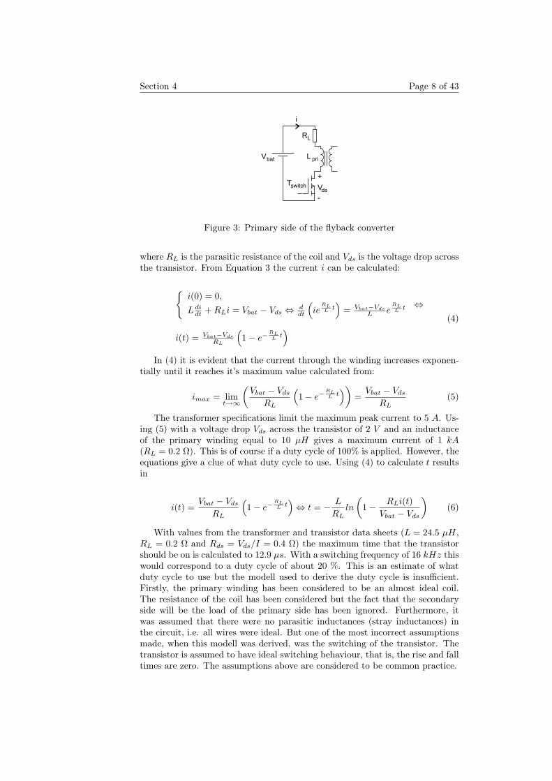
Considering Figure 3, it is possible to determine the voltage drop across, and thecurrent through the primary winding of the transformer (when the transistor ison).
The voltage drop across the primary winding of the transformer is easilydescribed by Equation 3.
Ldi
dt= Vbat − Vds −RLi, (3)
Section 4 Page 8 of 43
RL
Vbat L pri
Tswitch Vds
+
-
i
Figure 3: Primary side of the flyback converter
where RL is the parasitic resistance of the coil and Vds is the voltage drop acrossthe transistor. From Equation 3 the current i can be calculated:
i(0) = 0,
L didt + RLi = Vbat − Vds ⇔ d
dt
(ie
RLL t
)= Vbat−Vds
L eRLL t ⇔
i(t) = Vbat−Vds
RL
(1− e−
RLL t
) (4)
In (4) it is evident that the current through the winding increases exponen-tially until it reaches it’s maximum value calculated from:
imax = limt→∞
(Vbat − Vds
RL
(1− e−
RLL t
))=
Vbat − Vds
RL(5)
The transformer specifications limit the maximum peak current to 5 A. Us-ing (5) with a voltage drop Vds across the transistor of 2 V and an inductanceof the primary winding equal to 10 µH gives a maximum current of 1 kA(RL = 0.2 Ω). This is of course if a duty cycle of 100% is applied. However, theequations give a clue of what duty cycle to use. Using (4) to calculate t resultsin
i(t) =Vbat − Vds
RL
(1− e−
RLL t
)⇔ t = − L
RLln
(1− RLi(t)
Vbat − Vds
)(6)
With values from the transformer and transistor data sheets (L = 24.5 µH,RL = 0.2 Ω and Rds = Vds/I = 0.4 Ω) the maximum time that the transistorshould be on is calculated to 12.9 µs. With a switching frequency of 16 kHz thiswould correspond to a duty cycle of about 20 %. This is an estimate of whatduty cycle to use but the modell used to derive the duty cycle is insufficient.Firstly, the primary winding has been considered to be an almost ideal coil.The resistance of the coil has been considered but the fact that the secondaryside will be the load of the primary side has been ignored. Furthermore, itwas assumed that there were no parasitic inductances (stray inductances) inthe circuit, i.e. all wires were ideal. But one of the most incorrect assumptionsmade, when this modell was derived, was the switching of the transistor. Thetransistor is assumed to have ideal switching behaviour, that is, the rise and falltimes are zero. The assumptions above are considered to be common practice.
Page 9 of 43 Design of a Current Controlled Defibrillator
With this brief discussion it is clear that one factor is essential when it comesto driving a current through the primary side of the transformer, short rise andfall times of the transistor (di/dt large). Furthermore, leakage inductances fromthe transformer (Lλ) and stray inductances from the wires (Lδ) will cause thecurrent through the winding to rise more slowly. Hence two factors need to beconsidered:
• Short rise and fall times of the transistor (di/dt large).
• Minimize leakage inductances in the circuit.
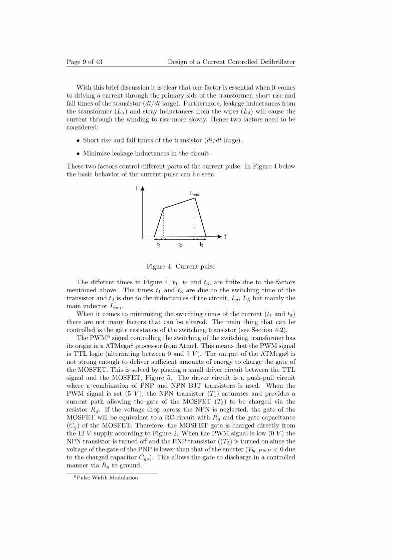
These two factors control different parts of the current pulse. In Figure 4 belowthe basic behavior of the current pulse can be seen.
t
iimax
t1 t2 t3
Figure 4: Current pulse
The different times in Figure 4, t1, t2 and t3, are finite due to the factorsmentioned above. The times t1 and t3 are due to the switching time of thetransistor and t2 is due to the inductances of the circuit, Lδ, Lλ but mainly themain inductor Lpri.
When it comes to minimizing the switching times of the current (t1 and t3)there are not many factors that can be altered. The main thing that can becontrolled is the gate resistance of the switching transistor (see Section 4.2).
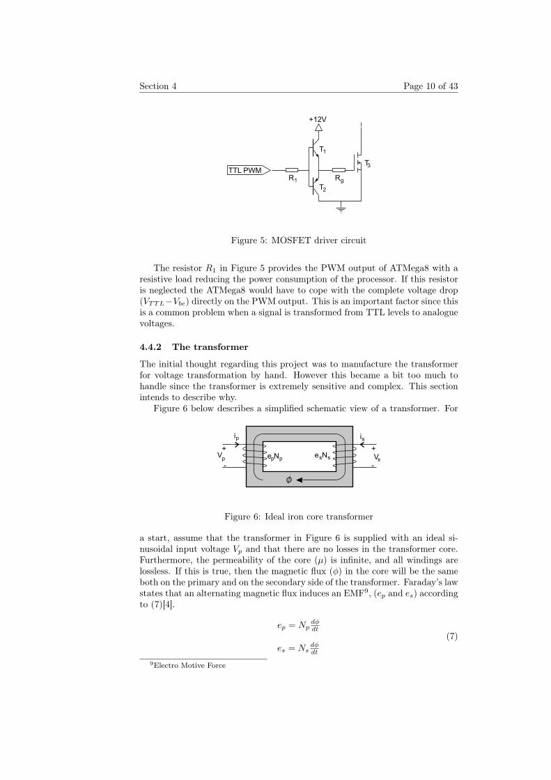
The PWM8 signal controlling the switching of the switching transformer hasits origin in a ATMega8 processor from Atmel. This means that the PWM signalis TTL logic (alternating between 0 and 5 V ). The output of the ATMega8 isnot strong enough to deliver sufficient amounts of energy to charge the gate ofthe MOSFET. This is solved by placing a small driver circuit between the TTLsignal and the MOSFET, Figure 5. The driver circuit is a push-pull circuitwhere a combination of PNP and NPN BJT transistors is used. When thePWM signal is set (5 V ), the NPN transistor (T1) saturates and provides acurrent path allowing the gate of the MOSFET (T3) to be charged via theresistor Rg. If the voltage drop across the NPN is neglected, the gate of theMOSFET will be equivalent to a RC-circuit with Rg and the gate capacitance(Cg) of the MOSFET. Therefore, the MOSFET gate is charged directly fromthe 12 V supply according to Figure 2. When the PWM signal is low (0 V ) theNPN transistor is turned off and the PNP transistor ((T2) is turned on since thevoltage of the gate of the PNP is lower than that of the emitter (Vbe,PNP < 0 dueto the charged capacitor Cgs). This allows the gate to discharge in a controlledmanner via Rg to ground.
8Pulse Width Modulation
Section 4 Page 10 of 43
+12V
T3
T2
T1
R1 Rg
TTL PWM
Figure 5: MOSFET driver circuit
The resistor R1 in Figure 5 provides the PWM output of ATMega8 with aresistive load reducing the power consumption of the processor. If this resistoris neglected the ATMega8 would have to cope with the complete voltage drop(VTTL−Vbe) directly on the PWM output. This is an important factor since thisis a common problem when a signal is transformed from TTL levels to analoguevoltages.
4.4.2 The transformer
The initial thought regarding this project was to manufacture the transformerfor voltage transformation by hand. However this became a bit too much tohandle since the transformer is extremely sensitive and complex. This sectionintends to describe why.
Figure 6 below describes a simplified schematic view of a transformer. For
O
+
-
+
-
Vp Vs
isip
e ppN e ssN
Figure 6: Ideal iron core transformer
a start, assume that the transformer in Figure 6 is supplied with an ideal si-nusoidal input voltage Vp and that there are no losses in the transformer core.Furthermore, the permeability of the core (µ) is infinite, and all windings arelossless. If this is true, then the magnetic flux (φ) in the core will be the sameboth on the primary and on the secondary side of the transformer. Faraday’s lawstates that an alternating magnetic flux induces an EMF9, (ep and es) accordingto (7)[4].
ep = Npdφdt
es = Nsdφdt
(7)
9Electro Motive Force
Page 11 of 43 Design of a Current Controlled Defibrillator
Since the magnetic flux is the same on both sides, the time derivative of themagnetic flux has to be the same too. Additionally the induced EMF should,ideally, be equal on both sides of the transformer. This makes it possible torewrite Equation 7.
ep
Np=
es
Ns⇔ Vp
Vs=
Np
Ns=
ep
es⇔ Vs = Vp
Ns
Np(8)
Sadly, real transformers are not ideal. In a real transformer there are leakageinductances, losses in the core, parasitic resistors and the magnetic permeability,µ, is far from infinity. A more accurate way to describe the transformer behaviorwith a non ideal transformer (µ < ∞) is using Equation 9,
Npip −Nsis =l
µSφ, (9)
where l is the length of the ferromagnetic core and S is the cross-sectional areaof the core [4].
When developing a transformer one has to take several factors into account:
• Core material, reducing eddy currents
• Size of the core
• Wire thickness
• Isolation voltage
• Efficiency of the transformer
One of the most important losses in a transformer core are the losses due to eddycurrents or Focault10 currents. Eddy currents are local currents induced by themagnetizing flux and flow in the normal direction of the flux. These currentsproduce ohmic power loss and cause local heating of the core. The losses dueto eddy currents can be reduced by using core materials with high permeability(µ) but low conductivity (σ). For low-frequency applications the most commonway to reduce the currents is by using laminated cores. The laminated cores areput together with an electrically isolating compound forcing the eddy currentsto propagate in each ’sheet’ of the core. As the frequency of the eddy currentsrise, the laminated cores behaves more and more like a solid core. For highfrequency applications a ferrite core is a better solution. The ferrite materialcan be described as made up of very small balls, where each ball is electricallyand magnetically isolated from its neighbors minimizing the area for the eddycurrents to propagate in.
The size of the core is essential since this determines the amount of magneticflux the core can hold without saturation. When a magnetic field intensity H isapplied to a ferromagnetic material a resulting magnetic field density, B, arisesin the material according to Equation 10.
B = µH (10)
Section 4 Page 12 of 43
B
H
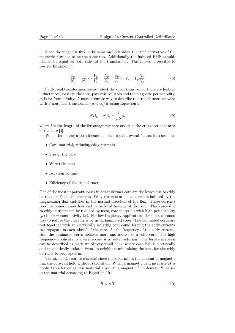
Figure 7: Hysteresis loop in the B-H plane for a ferromagnetic material
However, Equation 10 is not linear due to the fact that µ changes with the fieldintensity. This is due to remanent flux and saturation of the core, illustrated inFigure 7.
As seen in Figure 7 the magnetic flux density does not return to zero whenthe applied magnetic field intensity is zero. The remaining flux density in thematerial is called the residual or remanent flux density. It is also evident thata large applied magnetic field intensity will drive the core into saturation. Ifthe core is saturated, its magnetization does not increase with an increase inapplied magnetic field intensity.
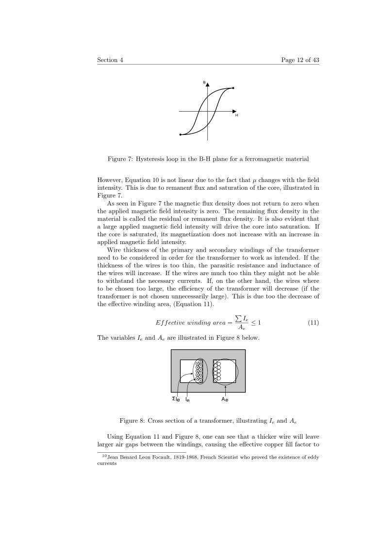
Wire thickness of the primary and secondary windings of the transformerneed to be considered in order for the transformer to work as intended. If thethickness of the wires is too thin, the parasitic resistance and inductance ofthe wires will increase. If the wires are much too thin they might not be ableto withstand the necessary currents. If, on the other hand, the wires whereto be chosen too large, the efficiency of the transformer will decrease (if thetransformer is not chosen unnecessarily large). This is due too the decrease ofthe effective winding area, (Equation 11).
Effective winding area =∑
Ie
Ae≤ 1 (11)
The variables Ie and Ae are illustrated in Figure 8 below.
IeIe Ae
Figure 8: Cross section of a transformer, illustrating Ie and Ae
Using Equation 11 and Figure 8, one can see that a thicker wire will leavelarger air gaps between the windings, causing the effective copper fill factor to
10Jean Benard Leon Focault, 1819-1868, French Scientist who proved the existence of eddycurrents
Page 13 of 43 Design of a Current Controlled Defibrillator
decrease since the number of turns has to be decreased in order for the windingsto fit in the available winding window Ae. This could be solved by using Litzwire or polarized wires (square wires). The inductance of a winding n of atransformer can be written as:
L = N2n
∑Ie
Aeµ0µr (12)
The voltage drop over a coil with inductance L can be written as:
VL = LdiLdt
(13)
Combining Equation 12 with Equation 13 result in Equation 14 [5].
VL = N2n
∑Ie
Aeµ0µr
diLdt
(14)
The voltage drop across the transformer should be maximized, which meansthat the effective winding quota,
∑Ie/Ae, should be as close to one as possible.
This also clarifies the need of accurate winding if the winding is done by hand.The wires should be as closely packed as possible and ideally no empty spaceshould be available in the winding window.
A good transformer also provides galvanic isolation between the primary andthe secondary winding. This isolation has to be taken into account when choos-ing wires. Since many cores have both the secondary and primary winding in thesame winding window it might be necessary to add an isolating sheet betweenthe windings, even though this will reduce the effective winding quota. Theisolation voltage also need to be experimentally verified before the transformercan be used in good faith.
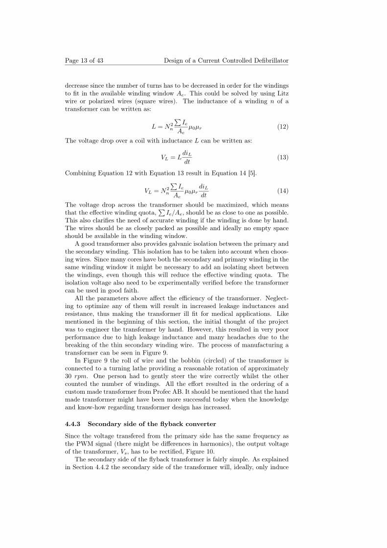
All the parameters above affect the efficiency of the transformer. Neglect-ing to optimize any of them will result in increased leakage inductances andresistance, thus making the transformer ill fit for medical applications. Likementioned in the beginning of this section, the initial thought of the projectwas to engineer the transformer by hand. However, this resulted in very poorperformance due to high leakage inductance and many headaches due to thebreaking of the thin secondary winding wire. The process of manufacturing atransformer can be seen in Figure 9.
In Figure 9 the roll of wire and the bobbin (circled) of the transformer isconnected to a turning lathe providing a reasonable rotation of approximately30 rpm. One person had to gently steer the wire correctly whilst the othercounted the number of windings. All the effort resulted in the ordering of acustom made transformer from Profec AB. It should be mentioned that the handmade transformer might have been more successful today when the knowledgeand know-how regarding transformer design has increased.
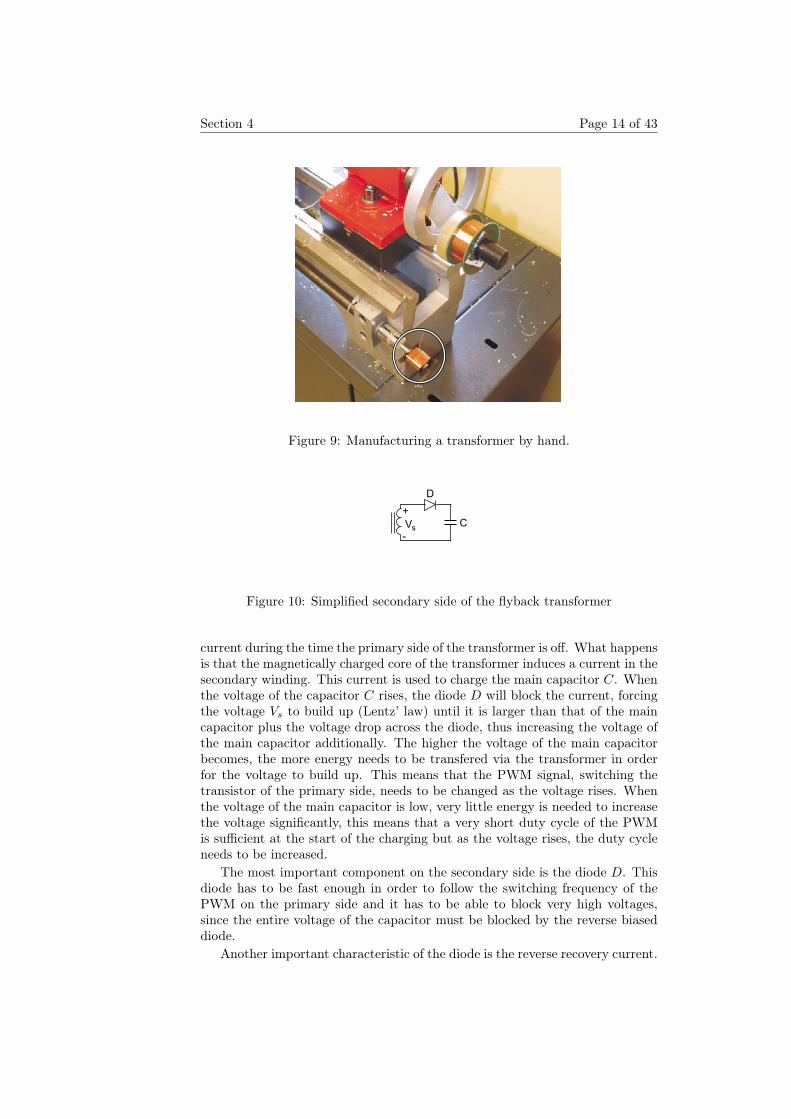
4.4.3 Secondary side of the flyback converter
Since the voltage transfered from the primary side has the same frequency asthe PWM signal (there might be differences in harmonics), the output voltageof the transformer, Vs, has to be rectified, Figure 10.
The secondary side of the flyback transformer is fairly simple. As explainedin Section 4.4.2 the secondary side of the transformer will, ideally, only induce
Section 4 Page 14 of 43
Figure 9: Manufacturing a transformer by hand.
V
D
C+
-s
Figure 10: Simplified secondary side of the flyback transformer
current during the time the primary side of the transformer is off. What happensis that the magnetically charged core of the transformer induces a current in thesecondary winding. This current is used to charge the main capacitor C. Whenthe voltage of the capacitor C rises, the diode D will block the current, forcingthe voltage Vs to build up (Lentz’ law) until it is larger than that of the maincapacitor plus the voltage drop across the diode, thus increasing the voltage ofthe main capacitor additionally. The higher the voltage of the main capacitorbecomes, the more energy needs to be transfered via the transformer in orderfor the voltage to build up. This means that the PWM signal, switching thetransistor of the primary side, needs to be changed as the voltage rises. Whenthe voltage of the main capacitor is low, very little energy is needed to increasethe voltage significantly, this means that a very short duty cycle of the PWMis sufficient at the start of the charging but as the voltage rises, the duty cycleneeds to be increased.
The most important component on the secondary side is the diode D. Thisdiode has to be fast enough in order to follow the switching frequency of thePWM on the primary side and it has to be able to block very high voltages,since the entire voltage of the capacitor must be blocked by the reverse biaseddiode.
Another important characteristic of the diode is the reverse recovery current.
Page 15 of 43 Design of a Current Controlled Defibrillator
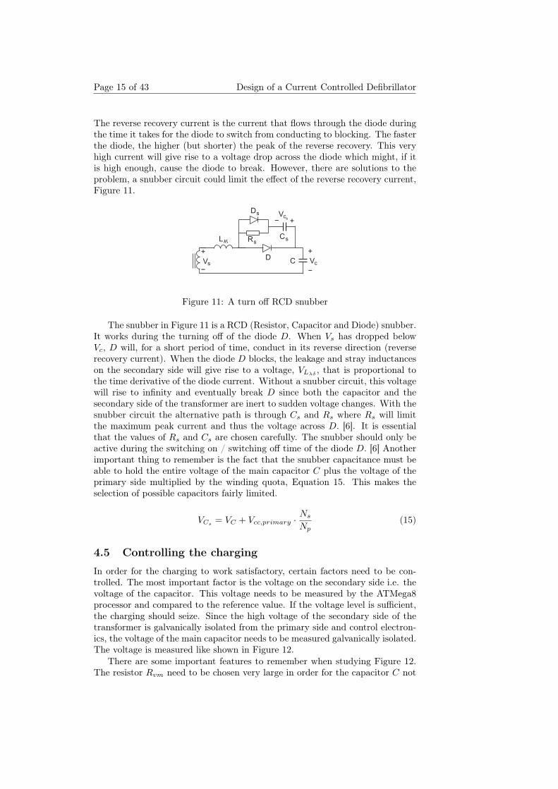
The reverse recovery current is the current that flows through the diode duringthe time it takes for the diode to switch from conducting to blocking. The fasterthe diode, the higher (but shorter) the peak of the reverse recovery. This veryhigh current will give rise to a voltage drop across the diode which might, if itis high enough, cause the diode to break. However, there are solutions to theproblem, a snubber circuit could limit the effect of the reverse recovery current,Figure 11.
V
V
D C
+
+
-
-
V
+
-s c
cs
RsCs
Ds
L
Figure 11: A turn off RCD snubber
The snubber in Figure 11 is a RCD (Resistor, Capacitor and Diode) snubber.It works during the turning off of the diode D. When Vs has dropped belowVc, D will, for a short period of time, conduct in its reverse direction (reverserecovery current). When the diode D blocks, the leakage and stray inductanceson the secondary side will give rise to a voltage, VLλδ
, that is proportional tothe time derivative of the diode current. Without a snubber circuit, this voltagewill rise to infinity and eventually break D since both the capacitor and thesecondary side of the transformer are inert to sudden voltage changes. With thesnubber circuit the alternative path is through Cs and Rs where Rs will limitthe maximum peak current and thus the voltage across D. [6]. It is essentialthat the values of Rs and Cs are chosen carefully. The snubber should only beactive during the switching on / switching off time of the diode D. [6] Anotherimportant thing to remember is the fact that the snubber capacitance must beable to hold the entire voltage of the main capacitor C plus the voltage of theprimary side multiplied by the winding quota, Equation 15. This makes theselection of possible capacitors fairly limited.
VCs= VC + Vcc,primary ·
Ns
Np(15)
4.5 Controlling the charging
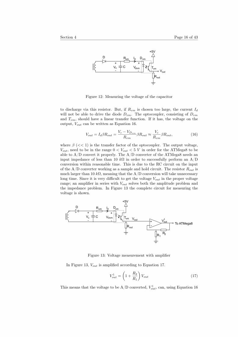
In order for the charging to work satisfactory, certain factors need to be con-trolled. The most important factor is the voltage on the secondary side i.e. thevoltage of the capacitor. This voltage needs to be measured by the ATMega8processor and compared to the reference value. If the voltage level is sufficient,the charging should seize. Since the high voltage of the secondary side of thetransformer is galvanically isolated from the primary side and control electron-ics, the voltage of the main capacitor needs to be measured galvanically isolated.The voltage is measured like shown in Figure 12.
There are some important features to remember when studying Figure 12.The resistor Rvm need to be chosen very large in order for the capacitor C not
Section 4 Page 16 of 43
+5V
Rvm DvmD
Vout
Rout
TvmC
+ +
- -Vc Vdvm
Id
Figure 12: Measuring the voltage of the capacitor
to discharge via this resistor. But, if Rvm is chosen too large, the current Id
will not be able to drive the diode Dvm. The optocoupler, consisting of Dvm
and Tvm, should have a linear transfer function. If it has, the voltage on theoutput, Vout can be written as Equation 16.
Vout = IdβRout =Vc − VDvm
RvmβRout ≈
Vc
RvmβRout, (16)
where β (<< 1) is the transfer factor of the optocoupler. The output voltage,Vout, need to be in the range 0 < Vout < 5 V in order for the ATMega8 to beable to A/D convert it properly. The A/D converter of the ATMega8 needs aninput impedance of less than 10 kΩ in order to successfully perform an A/Dconversion within reasonable time. This is due to the RC circuit on the inputof the A/D converter working as a sample and hold circuit. The resistor Rout ismuch larger than 10 kΩ, meaning that the A/D conversion will take unnecessarylong time. Since it is very difficult to get the voltage Vout in the proper voltagerange; an amplifier in series with Vout solves both the amplitude problem andthe impedance problem. In Figure 13 the complete circuit for measuring thevoltage is shown.
+5V
RvmD
Vout 1Vout
To ATMega8Rout
R1R2
TvmC
+ +
- -
Vc Vdvm
Id
+
-
Dvm
Figure 13: Voltage measurement with amplifier
In Figure 13, Vout is amplified according to Equation 17.
V 1out =
(1 +
R2
R1
)Vout (17)
This means that the voltage to be A/D converted, V 1out, can, using Equation 16
Page 17 of 43 Design of a Current Controlled Defibrillator
and Equation 17, be written as:
V 1out ≈
(1 +
R2
R1
)Vc
RvmβRout (18)
The factor between V 1out and Vc can be controlled by changing the factor R2/R1.
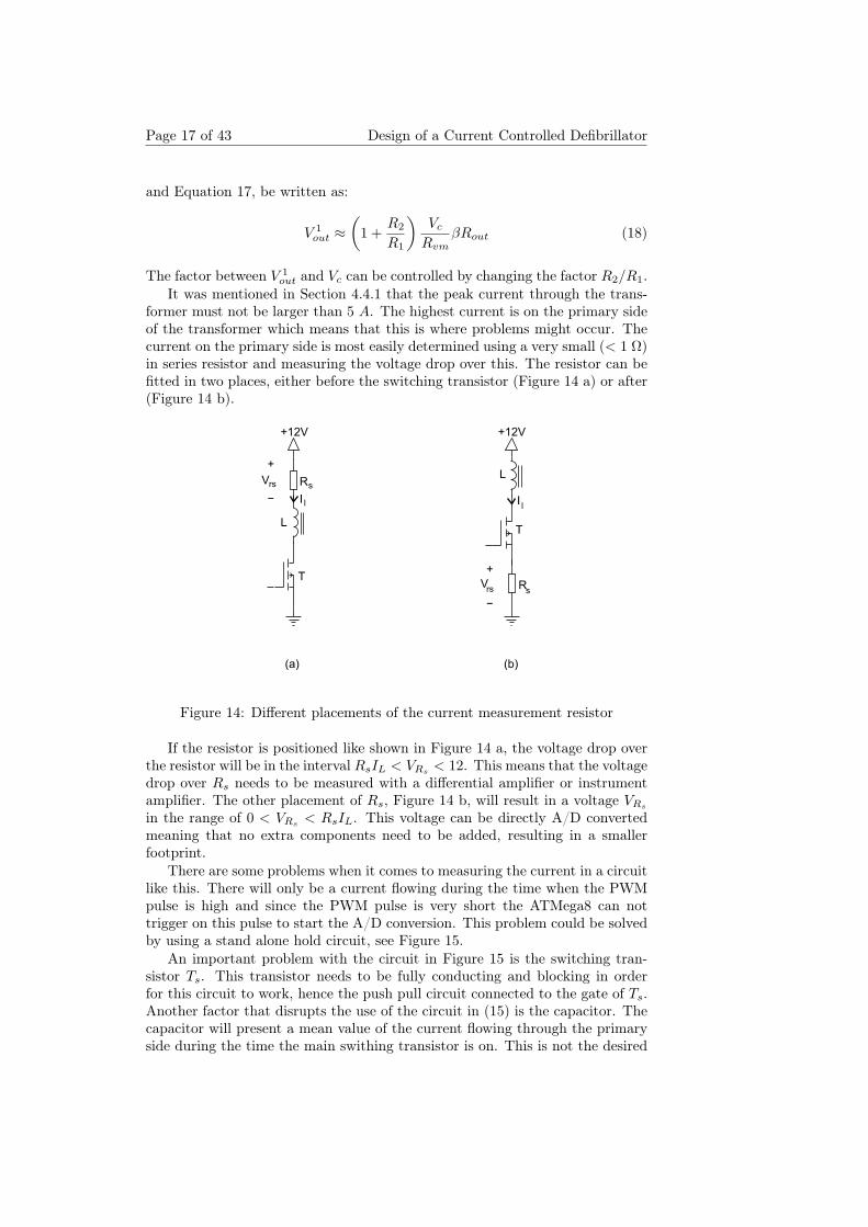
It was mentioned in Section 4.4.1 that the peak current through the trans-former must not be larger than 5 A. The highest current is on the primary sideof the transformer which means that this is where problems might occur. Thecurrent on the primary side is most easily determined using a very small (< 1 Ω)in series resistor and measuring the voltage drop over this. The resistor can befitted in two places, either before the switching transistor (Figure 14 a) or after(Figure 14 b).
(a) (b)
+12V
RsVrs
T
+
-
L
I l
+12V
Rs
Vrs
T
+
-
L
Il
Figure 14: Different placements of the current measurement resistor
If the resistor is positioned like shown in Figure 14 a, the voltage drop overthe resistor will be in the interval RsIL < VRs
< 12. This means that the voltagedrop over Rs needs to be measured with a differential amplifier or instrumentamplifier. The other placement of Rs, Figure 14 b, will result in a voltage VRs
in the range of 0 < VRs < RsIL. This voltage can be directly A/D convertedmeaning that no extra components need to be added, resulting in a smallerfootprint.
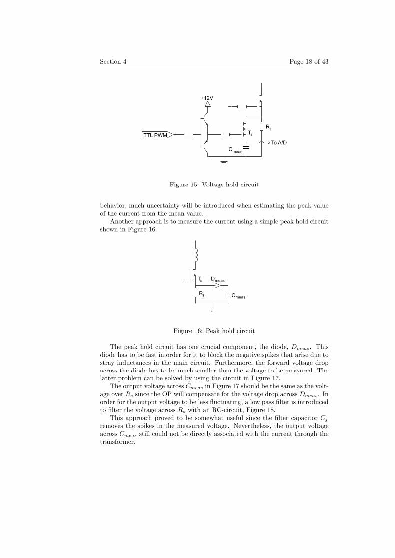
There are some problems when it comes to measuring the current in a circuitlike this. There will only be a current flowing during the time when the PWMpulse is high and since the PWM pulse is very short the ATMega8 can nottrigger on this pulse to start the A/D conversion. This problem could be solvedby using a stand alone hold circuit, see Figure 15.
An important problem with the circuit in Figure 15 is the switching tran-sistor Ts. This transistor needs to be fully conducting and blocking in orderfor this circuit to work, hence the push pull circuit connected to the gate of Ts.Another factor that disrupts the use of the circuit in (15) is the capacitor. Thecapacitor will present a mean value of the current flowing through the primaryside during the time the main swithing transistor is on. This is not the desired
Section 4 Page 18 of 43
+12V
TsTTL PWM
To A/D
Rl
Cmeas
Figure 15: Voltage hold circuit
behavior, much uncertainty will be introduced when estimating the peak valueof the current from the mean value.
Another approach is to measure the current using a simple peak hold circuitshown in Figure 16.
Ts
Rs
Dmeas
Cmeas
Figure 16: Peak hold circuit
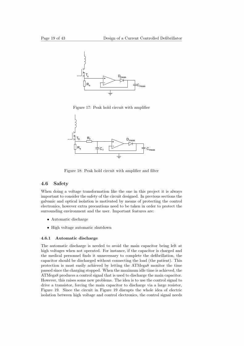
The peak hold circuit has one crucial component, the diode, Dmeas. Thisdiode has to be fast in order for it to block the negative spikes that arise due tostray inductances in the main circuit. Furthermore, the forward voltage dropacross the diode has to be much smaller than the voltage to be measured. Thelatter problem can be solved by using the circuit in Figure 17.
The output voltage across Cmeas in Figure 17 should be the same as the volt-age over Rs since the OP will compensate for the voltage drop across Dmeas. Inorder for the output voltage to be less fluctuating, a low pass filter is introducedto filter the voltage across Rs with an RC-circuit, Figure 18.
This approach proved to be somewhat useful since the filter capacitor Cf
removes the spikes in the measured voltage. Nevertheless, the output voltageacross Cmeas still could not be directly associated with the current through thetransformer.
Page 19 of 43 Design of a Current Controlled Defibrillator
Ts
Rs
Dmeas+
-Cmeas
Figure 17: Peak hold circuit with amplifier
TS
Rs
Rf
C f
Dmeas+
-Cmeas
Figure 18: Peak hold circuit with amplifier and filter
4.6 SafetyWhen doing a voltage transformation like the one in this project it is alwaysimportant to consider the safety of the circuit designed. In previous sections thegalvanic and optical isolation is motivated by means of protecting the controlelectronics, however extra precautions need to be taken in order to protect thesurrounding environment and the user. Important features are:
• Automatic discharge
• High voltage automatic shutdown
4.6.1 Automatic discharge
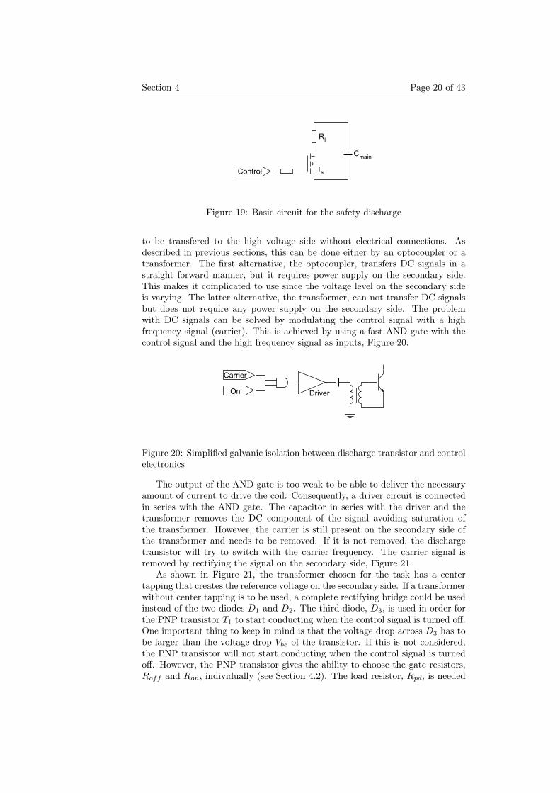
The automatic discharge is needed to avoid the main capacitor being left athigh voltages when not operated. For instance, if the capacitor is charged andthe medical personnel finds it unnecessary to complete the defibrillation, thecapacitor should be discharged without connecting the load (the patient). Thisprotection is most easily achieved by letting the ATMega8 monitor the timepassed since the charging stopped. When the maximum idle time is achieved, theATMega8 produces a control signal that is used to discharge the main capacitor.However, this raises some new problems. The idea is to use the control signal todrive a transistor, forcing the main capacitor to discharge via a large resistor,Figure 19. Since the circuit in Figure 19 disrupts the whole idea of electricisolation between high voltage and control electronics, the control signal needs
Section 4 Page 20 of 43
Ts
Rl
Cmain
Control
Figure 19: Basic circuit for the safety discharge
to be transfered to the high voltage side without electrical connections. Asdescribed in previous sections, this can be done either by an optocoupler or atransformer. The first alternative, the optocoupler, transfers DC signals in astraight forward manner, but it requires power supply on the secondary side.This makes it complicated to use since the voltage level on the secondary sideis varying. The latter alternative, the transformer, can not transfer DC signalsbut does not require any power supply on the secondary side. The problemwith DC signals can be solved by modulating the control signal with a highfrequency signal (carrier). This is achieved by using a fast AND gate with thecontrol signal and the high frequency signal as inputs, Figure 20.
Driver
Carrier
On
Figure 20: Simplified galvanic isolation between discharge transistor and controlelectronics
The output of the AND gate is too weak to be able to deliver the necessaryamount of current to drive the coil. Consequently, a driver circuit is connectedin series with the AND gate. The capacitor in series with the driver and thetransformer removes the DC component of the signal avoiding saturation ofthe transformer. However, the carrier is still present on the secondary side ofthe transformer and needs to be removed. If it is not removed, the dischargetransistor will try to switch with the carrier frequency. The carrier signal isremoved by rectifying the signal on the secondary side, Figure 21.
As shown in Figure 21, the transformer chosen for the task has a centertapping that creates the reference voltage on the secondary side. If a transformerwithout center tapping is to be used, a complete rectifying bridge could be usedinstead of the two diodes D1 and D2. The third diode, D3, is used in order forthe PNP transistor T1 to start conducting when the control signal is turned off.One important thing to keep in mind is that the voltage drop across D3 has tobe larger than the voltage drop Vbe of the transistor. If this is not considered,the PNP transistor will not start conducting when the control signal is turnedoff. However, the PNP transistor gives the ability to choose the gate resistors,Roff and Ron, individually (see Section 4.2). The load resistor, Rpd, is needed
Page 21 of 43 Design of a Current Controlled Defibrillator
D1
Ron
T1
Roff
D2
D3
Rpd
Figure 21: Rectifying the current
to create a well defined voltage on the base of the PNP transistor.
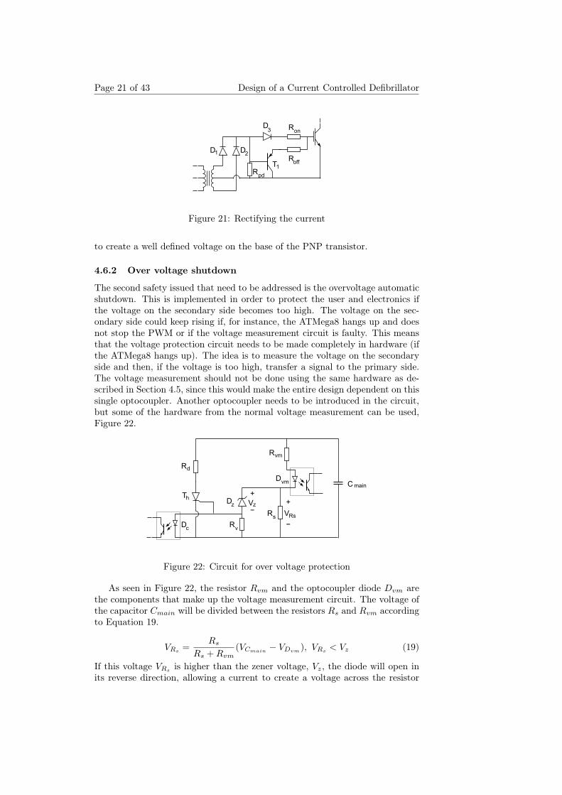
4.6.2 Over voltage shutdown
The second safety issued that need to be addressed is the overvoltage automaticshutdown. This is implemented in order to protect the user and electronics ifthe voltage on the secondary side becomes too high. The voltage on the sec-ondary side could keep rising if, for instance, the ATMega8 hangs up and doesnot stop the PWM or if the voltage measurement circuit is faulty. This meansthat the voltage protection circuit needs to be made completely in hardware (ifthe ATMega8 hangs up). The idea is to measure the voltage on the secondaryside and then, if the voltage is too high, transfer a signal to the primary side.The voltage measurement should not be done using the same hardware as de-scribed in Section 4.5, since this would make the entire design dependent on thissingle optocoupler. Another optocoupler needs to be introduced in the circuit,but some of the hardware from the normal voltage measurement can be used,Figure 22.
C main
++Vz
VRs-
-
Dvm
Rvm
Rv
Rd
Th
Rs
Dz
Dc
Figure 22: Circuit for over voltage protection
As seen in Figure 22, the resistor Rvm and the optocoupler diode Dvm arethe components that make up the voltage measurement circuit. The voltage ofthe capacitor Cmain will be divided between the resistors Rs and Rvm accordingto Equation 19.
VRs=
Rs
Rs + Rvm(VCmain
− VDvm), VRs
< Vz (19)
If this voltage VRsis higher than the zener voltage, Vz, the diode will open in
its reverse direction, allowing a current to create a voltage across the resistor
Section 4 Page 22 of 43
Rv. This voltage is the same as the driving voltage of the thyristor, TH , whichwill cause this to open and discharging the capacitor Cmain via Rd. Since thediode of the high voltage protection control signal optocoupler, Dc, is currentdriven, the current through Dc will not be linear but dependent on the voltageof the main capacitor according to Equation 20.
IDc= Is
(e
VDcVT − 1
), VDc
= VRs− Vz, VRs
> Vz (20)
In Equation 20, VT is the threshold voltage of Dc and Is is the saturationcurrent [1]. The voltage drop over the diode, VDc
, is determined by the voltagedrop over the resistor Rs which in turn is determined by the current throughthe diode when VRs
> Vz, Equation 21.
VRs= IRvm
− IDc= IRvm
− Is
(e
VRs−Vz
VT − 1)
(21)
Where IRvmis a function of the voltage drop across Dvm:
IRvm=
VCmain − VRs − VDvm
Rvm(22)
Equation 21 is not very easy to solve since the voltage drop over Dvm isdependent of the current through the resistor Rvm. This makes it hard to de-termine what value of Rs to use, hence experimental verification will be needed.
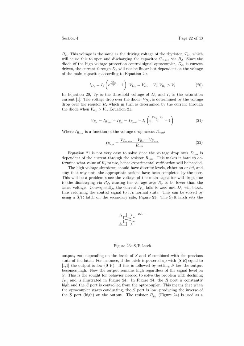
The high voltage shutdown should have discrete levels, either on or off, andstay that way until the appropriate actions have been completed by the user.This will be a problem since the voltage of the main capacitor will drop, dueto the discharging via Rd, causing the voltage over Rs to be lower than thezener voltage. Consequently, the current IDc falls to zero and Dz will block,thus returning the control signal to it’s normal state. This can be solved byusing a S/R latch on the secondary side, Figure 23. The S/R latch sets the
S
Rout
Figure 23: S/R latch
output, out, depending on the levels of S and R combined with the previousstate of the latch. For instance, if the latch is powered up with [S,R] equal to[1,1] the output is low (0 V ). If this is followed by setting S low the outputbecomes high. Now the output remains high regardless of the signal level onS. This is the sought for behavior needed to solve the problem with decliningIDc
and is illustrated in Figure 24. In Figure 24, the R port is constantlyhigh and the S port is controlled from the optocoupler. This means that whenthe optocoupler starts conducting, the S port is low, producing the inverse ofthe S port (high) on the output. The resistor Rpu
(Figure 24) is used as a
Page 23 of 43 Design of a Current Controlled Defibrillator
S
RR
HVSD
pu
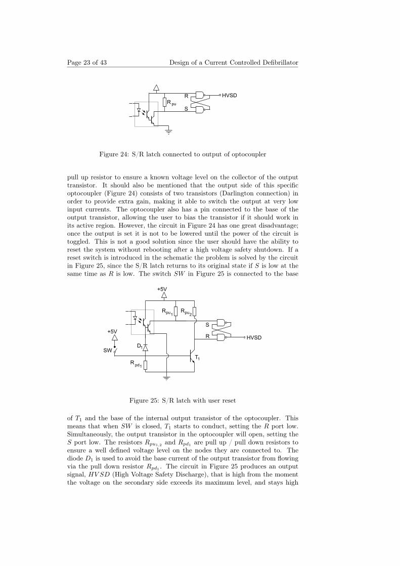
Figure 24: S/R latch connected to output of optocoupler
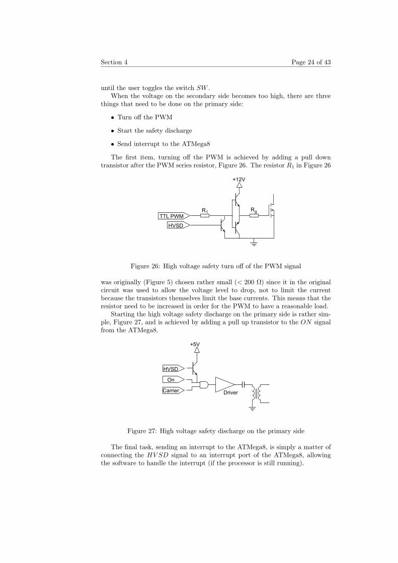
pull up resistor to ensure a known voltage level on the collector of the outputtransistor. It should also be mentioned that the output side of this specificoptocoupler (Figure 24) consists of two transistors (Darlington connection) inorder to provide extra gain, making it able to switch the output at very lowinput currents. The optocoupler also has a pin connected to the base of theoutput transistor, allowing the user to bias the transistor if it should work inits active region. However, the circuit in Figure 24 has one great disadvantage;once the output is set it is not to be lowered until the power of the circuit istoggled. This is not a good solution since the user should have the ability toreset the system without rebooting after a high voltage safety shutdown. If areset switch is introduced in the schematic the problem is solved by the circuitin Figure 25, since the S/R latch returns to its original state if S is low at thesame time as R is low. The switch SW in Figure 25 is connected to the base
+5V
T1
Rpu2
Rpu1
Rpd1
+5V
SWD1
HVSD
S
R
Figure 25: S/R latch with user reset
of T1 and the base of the internal output transistor of the optocoupler. Thismeans that when SW is closed, T1 starts to conduct, setting the R port low.Simultaneously, the output transistor in the optocoupler will open, setting theS port low. The resistors Rpu1,2 and Rpd1 are pull up / pull down resistors toensure a well defined voltage level on the nodes they are connected to. Thediode D1 is used to avoid the base current of the output transistor from flowingvia the pull down resistor Rpd1 . The circuit in Figure 25 produces an outputsignal, HV SD (High Voltage Safety Discharge), that is high from the momentthe voltage on the secondary side exceeds its maximum level, and stays high
Section 4 Page 24 of 43
until the user toggles the switch SW .When the voltage on the secondary side becomes too high, there are three
things that need to be done on the primary side:
• Turn off the PWM
• Start the safety discharge
• Send interrupt to the ATMega8
The first item, turning off the PWM is achieved by adding a pull downtransistor after the PWM series resistor, Figure 26. The resistor R1 in Figure 26
+12V
TTL PWM
HVSD
R1Rg
Figure 26: High voltage safety turn off of the PWM signal
was originally (Figure 5) chosen rather small (< 200 Ω) since it in the originalcircuit was used to allow the voltage level to drop, not to limit the currentbecause the transistors themselves limit the base currents. This means that theresistor need to be increased in order for the PWM to have a reasonable load.
Starting the high voltage safety discharge on the primary side is rather sim-ple, Figure 27, and is achieved by adding a pull up transistor to the ON signalfrom the ATMega8.
DriverCarrier
On
HVSD
+5V
Figure 27: High voltage safety discharge on the primary side
The final task, sending an interrupt to the ATMega8, is simply a matter ofconnecting the HV SD signal to an interrupt port of the ATMega8, allowingthe software to handle the interrupt (if the processor is still running).
Page 25 of 43 Design of a Current Controlled Defibrillator
5 DischargeAs mentioned numerous times before the behavior of the defibrillator shouldduring discharge (defibrillation) be biphasic. Applying the whole voltage of themain capacitor directly to the load (patient) would result in a current flowingconstantly from anode to cathode of the capacitor until it was completely dis-charged. In this section it is described how the development of the dischargingmodule was conducted and the underlying theory.
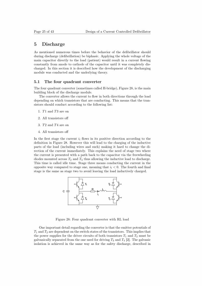
5.1 The four quadrant converterThe four quadrant converter (sometimes called H-bridge), Figure 28, is the mainbuilding block of the discharge module.
The converter allows the current to flow in both directions through the loaddepending on which transistors that are conducting. This means that the tran-sistors should conduct according to the following list:
1. T1 and T3 are on
2. All transistors off
3. T2 and T4 are on
4. All transistors off
In the first stage the current il flows in its positive direction according to thedefinition in Figure 28. However this will lead to the charging of the inductiveparts of the load (including wires and such) making it hard to change the di-rection of the current immediately. This explains the need of stage two wherethe current is presented with a path back to the capacitor via the freewheelingdiodes mounted across T2 and T4 thus allowing the inductive load to discharge.This time is called idle time. Stage three means conducting the current in theopposite way compared to stage one, meaning that il < 0. The fourth and finalstage is the same as stage two to avoid leaving the load inductively charged.
T1
il
RC
L
T3T4
T2
Figure 28: Four quadrant converter with RL load
One important detail regarding the converter is that the emitter potentials ofT1 and T2 are dependent on the switch states of the transistors. This implies thatthe power supplies for the driver circuits of both transistors T1 and T2 must begalvanically separated from the one used for driving T3 and T4 [2]. The galvanicisolation is achieved in the same way as for the safety discharge, described in
Section 5 Page 26 of 43
Section 4.6.2. Since all transistors need to be controlled independently, fourdifferent circuits like the ones described in Figure 21 are needed.
5.2 Controlling the discharge
The need for some kind of controller for the discharge is evident. If one is notused (old defibrillators) the entire voltage of the capacitor will be applied acrossthe load and the resistive and inductive parts of the load will be the only factorslimiting the current. It was mentioned in earlier sections that current control isan important feature that should be implemented in the device.
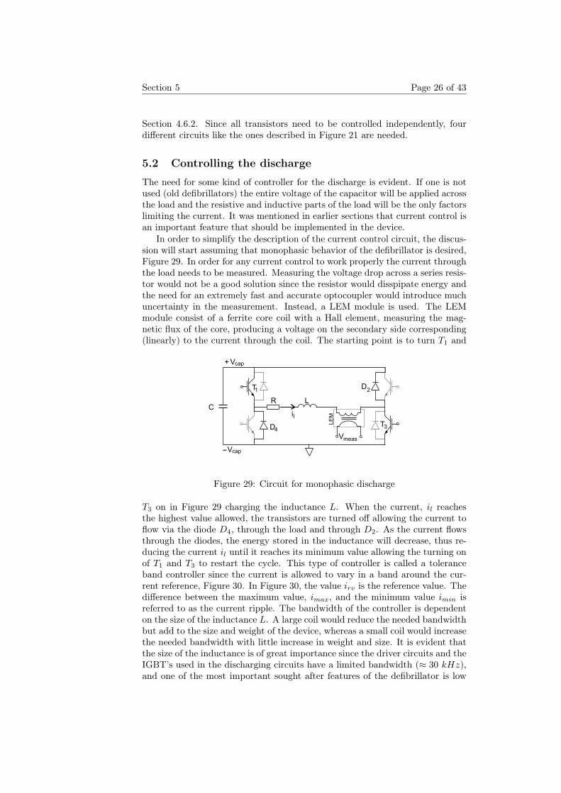
In order to simplify the description of the current control circuit, the discus-sion will start assuming that monophasic behavior of the defibrillator is desired,Figure 29. In order for any current control to work properly the current throughthe load needs to be measured. Measuring the voltage drop across a series resis-tor would not be a good solution since the resistor would disspipate energy andthe need for an extremely fast and accurate optocoupler would introduce muchuncertainty in the measurement. Instead, a LEM module is used. The LEMmodule consist of a ferrite core coil with a Hall element, measuring the mag-netic flux of the core, producing a voltage on the secondary side corresponding(linearly) to the current through the coil. The starting point is to turn T1 and
T1
il
RC
LE
M
-
+
Vmeas
Vcap
Vcap
L
T3D4
D2
Figure 29: Circuit for monophasic discharge
T3 on in Figure 29 charging the inductance L. When the current, il reachesthe highest value allowed, the transistors are turned off allowing the current toflow via the diode D4, through the load and through D2. As the current flowsthrough the diodes, the energy stored in the inductance will decrease, thus re-ducing the current il until it reaches its minimum value allowing the turning onof T1 and T3 to restart the cycle. This type of controller is called a toleranceband controller since the current is allowed to vary in a band around the cur-rent reference, Figure 30. In Figure 30, the value irv is the reference value. Thedifference between the maximum value, imax, and the minimum value imin isreferred to as the current ripple. The bandwidth of the controller is dependenton the size of the inductance L. A large coil would reduce the needed bandwidthbut add to the size and weight of the device, whereas a small coil would increasethe needed bandwidth with little increase in weight and size. It is evident thatthe size of the inductance is of great importance since the driver circuits and theIGBT’s used in the discharging circuits have a limited bandwidth (≈ 30 kHz),and one of the most important sought after features of the defibrillator is low
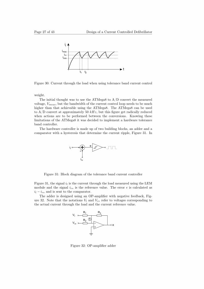
Page 27 of 43 Design of a Current Controlled Defibrillator
t
il
imax
imin
t1 t2
irv
Figure 30: Current through the load when using tolerance band current control
weight.The initial thought was to use the ATMega8 to A/D convert the measured
voltage, Vmeas, but the bandwidth of the current control loop needs to be muchhigher than that achievable using the ATMega8. The ATMega8 can be usedto A/D convert at approximately 50 kHz, but this figure get radically reducedwhen actions are to be performed between the conversions. Knowing theselimitations of the ATMega8 it was decided to implement a hardware toleranceband controller.
The hardware controller is made up of two building blocks, an adder and acomparator with a hysteresis that determine the current ripple, Figure 31. In
il
irv
e
-
Figure 31: Block diagram of the tolerance band current controller
Figure 31, the signal il is the current through the load measured using the LEMmodule and the signal irv is the reference value. The error e is calculated asil − irv and is sent to the comparator.
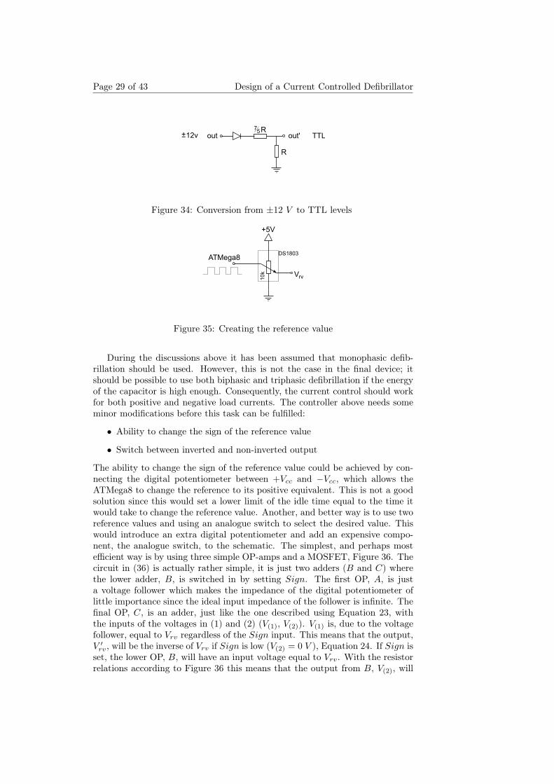
The adder is designed using an OP-amplifier with negative feedback, Fig-ure 32. Note that the notations Vl and Vrv refer to voltages corresponding tothe actual current through the load and the current reference value.
R1Vl
eVrv
R2
R3
+
-
Figure 32: OP-amplifier adder
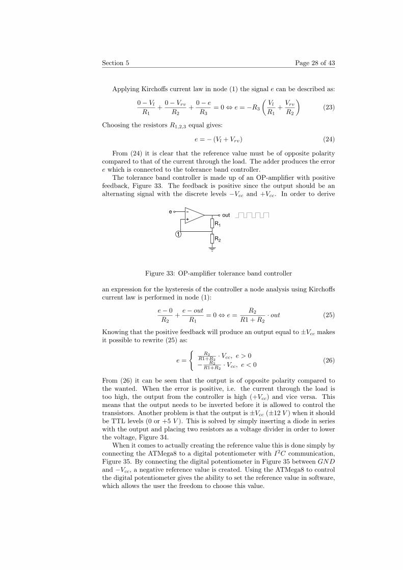
Section 5 Page 28 of 43
Applying Kirchoffs current law in node (1) the signal e can be described as:
0− Vl
R1+
0− Vrv
R2+
0− e
R3= 0 ⇔ e = −R3
(Vl
R1+
Vrv
R2
)(23)
Choosing the resistors R1,2,3 equal gives:
e = − (Vl + Vrv) (24)
From (24) it is clear that the reference value must be of opposite polaritycompared to that of the current through the load. The adder produces the errore which is connected to the tolerance band controller.
The tolerance band controller is made up of an OP-amplifier with positivefeedback, Figure 33. The feedback is positive since the output should be analternating signal with the discrete levels −Vcc and +Vcc. In order to derive
R1
oute
R2
+
-
Figure 33: OP-amplifier tolerance band controller
an expression for the hysteresis of the controller a node analysis using Kirchoffscurrent law is performed in node (1):
e− 0R2
+e− out
R1= 0 ⇔ e =
R2
R1 + R2· out (25)
Knowing that the positive feedback will produce an output equal to ±Vcc makesit possible to rewrite (25) as:
e =
R2
R1+R2· Vcc, e > 0
− R2R1+R2
· Vcc, e < 0(26)
From (26) it can be seen that the output is of opposite polarity compared tothe wanted. When the error is positive, i.e. the current through the load istoo high, the output from the controller is high (+Vcc) and vice versa. Thismeans that the output needs to be inverted before it is allowed to control thetransistors. Another problem is that the output is ±Vcc (±12 V ) when it shouldbe TTL levels (0 or +5 V ). This is solved by simply inserting a diode in serieswith the output and placing two resistors as a voltage divider in order to lowerthe voltage, Figure 34.
When it comes to actually creating the reference value this is done simply byconnecting the ATMega8 to a digital potentiometer with I2C communication,Figure 35. By connecting the digital potentiometer in Figure 35 between GNDand −Vcc, a negative reference value is created. Using the ATMega8 to controlthe digital potentiometer gives the ability to set the reference value in software,which allows the user the freedom to choose this value.
Page 29 of 43 Design of a Current Controlled Defibrillator
R
out TTLout'12v+-R7
5
Figure 34: Conversion from ±12 V to TTL levels
ATMega8
Vrv
+5V
DS1803
10
k
Figure 35: Creating the reference value
During the discussions above it has been assumed that monophasic defib-rillation should be used. However, this is not the case in the final device; itshould be possible to use both biphasic and triphasic defibrillation if the energyof the capacitor is high enough. Consequently, the current control should workfor both positive and negative load currents. The controller above needs someminor modifications before this task can be fulfilled:
• Ability to change the sign of the reference value
• Switch between inverted and non-inverted output
The ability to change the sign of the reference value could be achieved by con-necting the digital potentiometer between +Vcc and −Vcc, which allows theATMega8 to change the reference to its positive equivalent. This is not a goodsolution since this would set a lower limit of the idle time equal to the time itwould take to change the reference value. Another, and better way is to use tworeference values and using an analogue switch to select the desired value. Thiswould introduce an extra digital potentiometer and add an expensive compo-nent, the analogue switch, to the schematic. The simplest, and perhaps mostefficient way is by using three simple OP-amps and a MOSFET, Figure 36. Thecircuit in (36) is actually rather simple, it is just two adders (B and C) wherethe lower adder, B, is switched in by setting Sign. The first OP, A, is justa voltage follower which makes the impedance of the digital potentiometer oflittle importance since the ideal input impedance of the follower is infinite. Thefinal OP, C, is an adder, just like the one described using Equation 23, withthe inputs of the voltages in (1) and (2) (V(1), V(2)). V(1) is, due to the voltagefollower, equal to Vrv regardless of the Sign input. This means that the output,V ′rv, will be the inverse of Vrv if Sign is low (V(2) = 0 V ), Equation 24. If Sign isset, the lower OP, B, will have an input voltage equal to Vrv. With the resistorrelations according to Figure 36 this means that the output from B, V(2), will
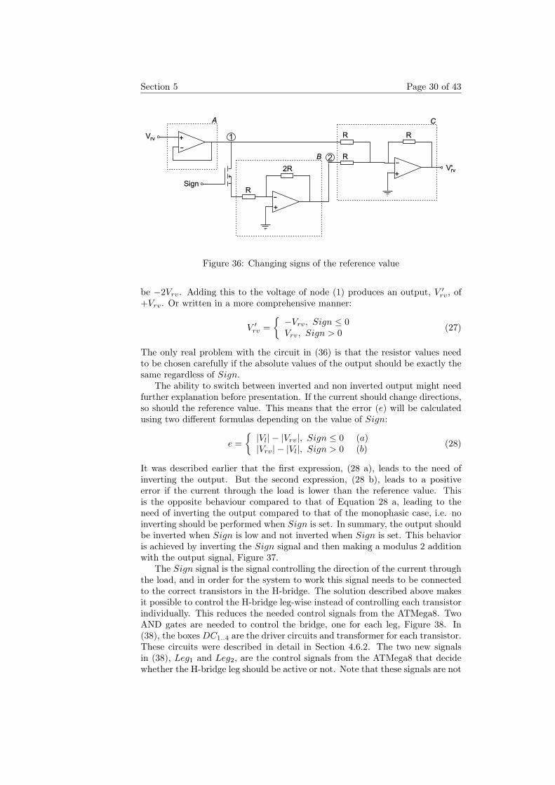
Section 5 Page 30 of 43
R
2R
+
-
R
R
Sign
A
B
C
R
+
-
Vrv
V'rv
+
-
Figure 36: Changing signs of the reference value
be −2Vrv. Adding this to the voltage of node (1) produces an output, V ′rv, of+Vrv. Or written in a more comprehensive manner:
V ′rv =−Vrv, Sign ≤ 0Vrv, Sign > 0 (27)
The only real problem with the circuit in (36) is that the resistor values needto be chosen carefully if the absolute values of the output should be exactly thesame regardless of Sign.
The ability to switch between inverted and non inverted output might needfurther explanation before presentation. If the current should change directions,so should the reference value. This means that the error (e) will be calculatedusing two different formulas depending on the value of Sign:
e =|Vl| − |Vrv|, Sign ≤ 0 (a)|Vrv| − |Vl|, Sign > 0 (b) (28)
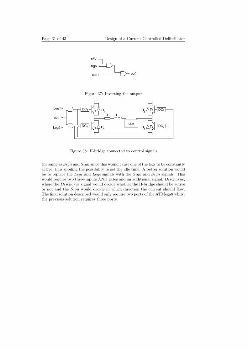
It was described earlier that the first expression, (28 a), leads to the need ofinverting the output. But the second expression, (28 b), leads to a positiveerror if the current through the load is lower than the reference value. Thisis the opposite behaviour compared to that of Equation 28 a, leading to theneed of inverting the output compared to that of the monophasic case, i.e. noinverting should be performed when Sign is set. In summary, the output shouldbe inverted when Sign is low and not inverted when Sign is set. This behavioris achieved by inverting the Sign signal and then making a modulus 2 additionwith the output signal, Figure 37.
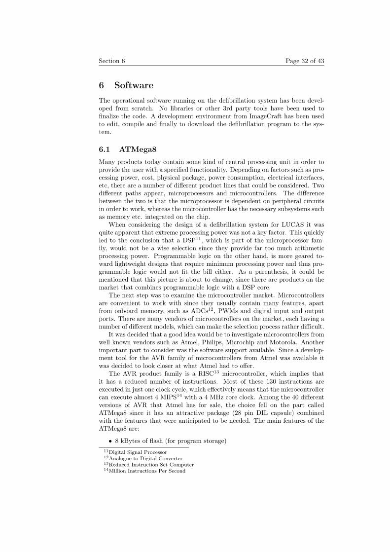
The Sign signal is the signal controlling the direction of the current throughthe load, and in order for the system to work this signal needs to be connectedto the correct transistors in the H-bridge. The solution described above makesit possible to control the H-bridge leg-wise instead of controlling each transistorindividually. This reduces the needed control signals from the ATMega8. TwoAND gates are needed to control the bridge, one for each leg, Figure 38. In(38), the boxes DC1..4 are the driver circuits and transformer for each transistor.These circuits were described in detail in Section 4.6.2. The two new signalsin (38), Leg1 and Leg2, are the control signals from the ATMega8 that decidewhether the H-bridge leg should be active or not. Note that these signals are not
Page 31 of 43 Design of a Current Controlled Defibrillator
+5V
sign
out out'
Figure 37: Inverting the output
T1
T4
R
Leg1
Leg2
L
T3
T2
D4
D1
D2
D3
out'
LEM
Figure 38: H-bridge connected to control signals
the same as Sign and Sign since this would cause one of the legs to be constantlyactive, thus spoiling the possibility to set the idle time. A better solution wouldbe to replace the Leg1 and Leg2 signals with the Sign and Sign signals. Thiswould require two three-inputs AND gates and an additional signal, Discharge,where the Discharge signal would decide whether the H-bridge should be activeor not and the Sign would decide in which direction the current should flow.The final solution described would only require two ports of the ATMega8 whilstthe previous solution requires three ports.
Section 6 Page 32 of 43
6 SoftwareThe operational software running on the defibrillation system has been devel-oped from scratch. No libraries or other 3rd party tools have been used tofinalize the code. A development environment from ImageCraft has been usedto edit, compile and finally to download the defibrillation program to the sys-tem.
6.1 ATMega8Many products today contain some kind of central processing unit in order toprovide the user with a specified functionality. Depending on factors such as pro-cessing power, cost, physical package, power consumption, electrical interfaces,etc, there are a number of different product lines that could be considered. Twodifferent paths appear, microprocessors and microcontrollers. The differencebetween the two is that the microprocessor is dependent on peripheral circuitsin order to work, whereas the microcontroller has the necessary subsystems suchas memory etc. integrated on the chip.
When considering the design of a defibrillation system for LUCAS it wasquite apparent that extreme processing power was not a key factor. This quicklyled to the conclusion that a DSP11, which is part of the microprocessor fam-ily, would not be a wise selection since they provide far too much arithmeticprocessing power. Programmable logic on the other hand, is more geared to-ward lightweight designs that require minimum processing power and thus pro-grammable logic would not fit the bill either. As a parenthesis, it could bementioned that this picture is about to change, since there are products on themarket that combines programmable logic with a DSP core.
The next step was to examine the microcontroller market. Microcontrollersare convenient to work with since they usually contain many features, apartfrom onboard memory, such as ADCs12, PWMs and digital input and outputports. There are many vendors of microcontrollers on the market, each having anumber of different models, which can make the selection process rather difficult.
It was decided that a good idea would be to investigate microcontrollers fromwell known vendors such as Atmel, Philips, Microchip and Motorola. Anotherimportant part to consider was the software support available. Since a develop-ment tool for the AVR family of microcontrollers from Atmel was available itwas decided to look closer at what Atmel had to offer.
The AVR product family is a RISC13 microcontroller, which implies thatit has a reduced number of instructions. Most of these 130 instructions areexecuted in just one clock cycle, which effectively means that the microcontrollercan execute almost 4 MIPS14 with a 4 MHz core clock. Among the 40 differentversions of AVR that Atmel has for sale, the choice fell on the part calledATMega8 since it has an attractive package (28 pin DIL capsule) combinedwith the features that were anticipated to be needed. The main features of theATMega8 are:
• 8 kBytes of flash (for program storage)11Digital Signal Processor12Analogue to Digital Converter13Reduced Instruction Set Computer14Million Instructions Per Second
Page 33 of 43 Design of a Current Controlled Defibrillator
• 512 bytes of EEPROM15 (for permanent data storage)
• 1024 bytes of SRAM16 (for program variables)
• 23 IO17 pins (used for digital input and output)
• 2 external interrupts (used for trigging on external events)
• I2C bus (for communicating with external circuits)
• 8 channel 10-bit ADC (used for measuring analogue signals)
• 2 timers (used for accurate timing needs)
• 3 PWM channels (used for controlling motors etc)
6.2 Overview
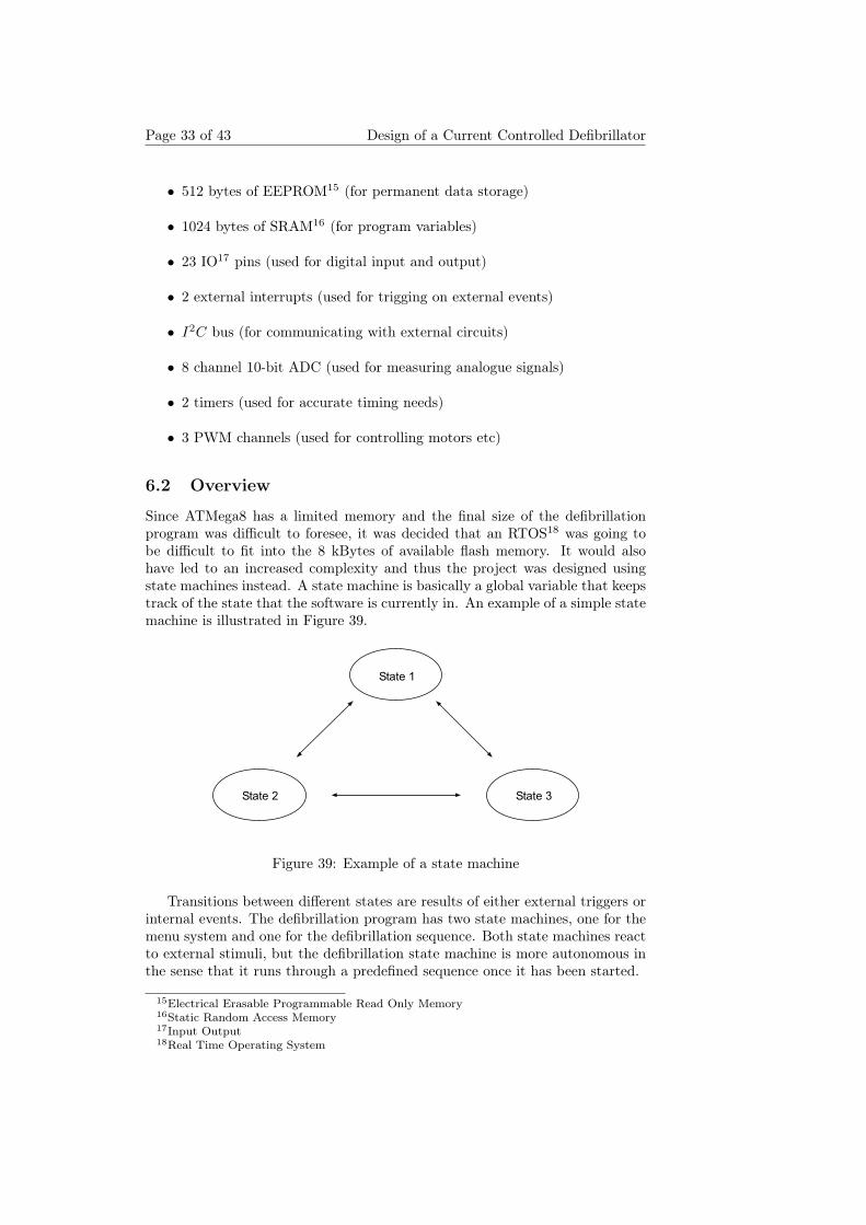
Since ATMega8 has a limited memory and the final size of the defibrillationprogram was difficult to foresee, it was decided that an RTOS18 was going tobe difficult to fit into the 8 kBytes of available flash memory. It would alsohave led to an increased complexity and thus the project was designed usingstate machines instead. A state machine is basically a global variable that keepstrack of the state that the software is currently in. An example of a simple statemachine is illustrated in Figure 39.
State 1
State 3State 2
Figure 39: Example of a state machine
Transitions between different states are results of either external triggers orinternal events. The defibrillation program has two state machines, one for themenu system and one for the defibrillation sequence. Both state machines reactto external stimuli, but the defibrillation state machine is more autonomous inthe sense that it runs through a predefined sequence once it has been started.
15Electrical Erasable Programmable Read Only Memory16Static Random Access Memory17Input Output18Real Time Operating System

Section 6 Page 34 of 43
6.3 Menu systemThe menu system is handled by a menu state machine which present a UI19 ona small 2 by 16 character display, connected to the defibrillation system via aserial interface. The UI, shown in C.1, enables the user to change importantdefibrillation parameters as well as initiate a defibrillation. This is done by usingthe four menu buttons +, -, Enter and a Cancel which together mimics a menubehavior similar to that of early mobile phones.
The parameters and their functions are described using an example of atriphasic discharge shown in Figure 40.
6.3.1 Charge voltage
This is the voltage that the main capacitor is charged to. This gives the user anidea of how much energy that is available for defibrillation. The voltage level isselectable from 100 to 1350 V in steps of 50 V .
6.3.2 Discharge type
This menu option enables the user to determine which kind of defibrillationthat should take place. The options are monophasic, biphasic and triphasicdefibrillation. Depending on the selected discharge type, the menu options Phaselength and Idle time have different number of submenus.
6.3.3 Current control
This menu option determines if the defibrillation should be current controlledor not. If the user selects Yes the current setting in menu Discharge curr. isused. If No is selected, the menu option Discharge curr. is not visible and amaximum discharge current of 25 A is used.
6.3.4 Phase length
This menu has different submenus depending on the selected Discharge type. Ifa triphasic defibrillation has been selected as in Figure 40, this submenu willenable the user to specify the length of A1, A2 and A3 in quarters of milliseconds.
6.3.5 Safety time
When the user initiates a charge of the main capacitor and the specified voltageselected by Charge voltage is reached, the Safety time value determines thenumber of seconds that this voltage will be maintained before an automaticsafety discharge will take place.
6.3.6 Idle time
This menu option contains a submenu where the user can edit the time intervalbetween a positive and a negative discharge. If a triphasic defibrillation isperformed, as done in (40), this sub menu enables the user to edit B1 and B2
in milliseconds. If a monophasic defibrillation is selected, this menu has noeditable parameters.
19User Interface
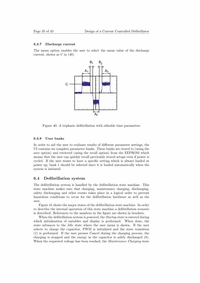
Page 35 of 43 Design of a Current Controlled Defibrillator
6.3.7 Discharge current
The menu option enables the user to select the mean value of the dischargecurrent, shown as C in (40).
3->
A1
B1 B2
A3
A2
C
Figure 40: A triphasic defibrillation with editable time parameters
6.3.8 User banks
In order to aid the user to evaluate results of different parameter settings, theUI contains six complete parameter banks. These banks are stored to (using thesave option) and retrieved (using the recall option) from the EEPROM whichmeans that the user can quickly recall previously stored setups even if power iscycled. If the user wants to have a specific setting which is always loaded atpower up, bank 1 should be selected since it is loaded automatically when thesystem is initiated.
6.4 Defibrillation system
The defibrillation system is handled by the defibrillation state machine. Thisstate machine makes sure that charging, maintenance charging, discharging,safety discharging and other events takes place in a logical order to preventhazardous conditions to occur for the defibrillation hardware as well as theuser.
Figure 41 shows the major states of the defibrillation state machine. In orderto describe the internal operation of this state machine a defibrillation scenariois described. References to the numbers in the figure are shown in brackets.
When the defibrillation system is powered, the Startup state is entered duringwhich initialization of variables and display is performed. When done, thestate advances to the Idle state where the user menu is shown. If the userselects to charge the capacitor, PWM is initialized and the state transition(1) is performed. If the user presses Cancel during the charging process, thecharging is stopped and the energy in the capacitor is safely discharged (8).When the requested voltage has been reached, the Maintenance Charging state
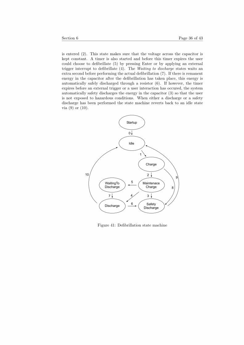
Section 6 Page 36 of 43
is entered (2). This state makes sure that the voltage across the capacitor iskept constant. A timer is also started and before this timer expires the usercould choose to defibrillate (5) by pressing Enter or by applying an externaltrigger interrupt to defibrillate (4). The Waiting to discharge states waits anextra second before performing the actual defibrillation (7). If there is remanentenergy in the capacitor after the defibrillation has taken place, this energy isautomatically safely discharged through a resistor (6). If however, the timerexpires before an external trigger or a user interaction has occured, the systemautomatically safety discharges the energy in the capacitor (3) so that the useris not exposed to hazardous conditions. When either a discharge or a safetydischarge has been performed the state machine reverts back to an idle statevia (9) or (10).
Startup
Idle
Discharge
WaitingToDischarge
Charge
MaintenaceCharge
SafetyDischarge
1
2
34
5
6
7
8
910
0
Figure 41: Defibrillation state machine
Page 37 of 43 Design of a Current Controlled Defibrillator
7 ResultThis section describes the results and final solutions regarding the defibrillatorand could be read somewhat separately by those who have little interest in theunderlying electrical theory. The final solution consists of three separate PCB’s:
• Charge and over voltage protection circuitry
• Discharge circuitry
• ATMega8 and current control circuitry
All the PCB’s were created using the Eagle software from Cadsoft and man-ufactured at the department of industrial electrical engineering and automation.All plots of measured results were achieved using a Tektronix TDS2002 oscillo-scope together with the WaveStar software.
7.1 ChargingThe final version of the charging module consists of one PCB containing thecharging electronics and the over voltage protection circuit described in Section4.6. A complete schematic of the charging board is presented in B.2.1 and thePCB layout in B.2.2.
The only major difficulty encountered when designing the charging circuitrywas the current measurement of the primary side. In the beginning of theproject the idea was to measure this current and optimize the duty cycle ofthe switching transistor, so that the current through the primary windings ofthe transformer would never exceed 5 A. Despite extensive research and ex-perimenting, the current could never be accurately measured with the systemprocessor generating the PWM pulse. However, if a fast stand alone circuit forgenerating the PWM and measuring the current was to be used, the bandwidthof this circuit might be enough to measure the current directly without havingto use mean value approximation or peak hold circuits.
The need for safety distances between signals on the high voltage side of thePCB was learned the hard way and no compromises have been made in the finaldesign regarding isolation distances.
The final version of the charging PCB is capable of charging a 44.1 µFcapacitor from 12 V DC to about 1350 V DC in 12 seconds, Figure 42. Thisequals a total energy of W = C · U2/2 ≈ 43.2 Joule. Note that the plot in(42) only goes as far as 1200 V . This is a known measurement error and theactual peak voltage of the capacitor is 1350 V . It is possible to achieve highervoltage levels but since the IGBT controlling the safety discharge is limited toVce ≤ 1500 V , higher secondary voltage is not recommended with this transistor.The charging time mentioned above will of course increase if a larger capacitorwas to be charged, but this would be the only difference in respect of the chargingelectronics.
The 16 kHz PWM signal used to boost the voltage is of incremental dutycycle, since a constant duty cycle would cause charging time for the last hun-dreds of volts to be very long. The incremental duty cycle algorithm utilizesfixed values dependent on the voltage of the capacitor. These values has beenexperimentally deduced and optimized so that the average current consumptionis below 600 mA during charging.
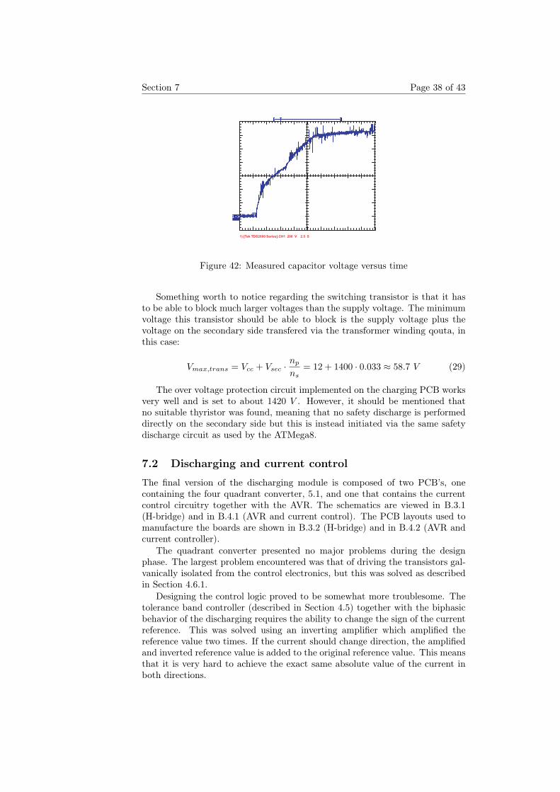
Section 7 Page 38 of 43
T1->
1) [Tek TDS2000 Series].CH1 200 V 2.5 S
Figure 42: Measured capacitor voltage versus time
Something worth to notice regarding the switching transistor is that it hasto be able to block much larger voltages than the supply voltage. The minimumvoltage this transistor should be able to block is the supply voltage plus thevoltage on the secondary side transfered via the transformer winding qouta, inthis case:
Vmax,trans = Vcc + Vsec ·np
ns= 12 + 1400 · 0.033 ≈ 58.7 V (29)
The over voltage protection circuit implemented on the charging PCB worksvery well and is set to about 1420 V . However, it should be mentioned thatno suitable thyristor was found, meaning that no safety discharge is performeddirectly on the secondary side but this is instead initiated via the same safetydischarge circuit as used by the ATMega8.
7.2 Discharging and current control
The final version of the discharging module is composed of two PCB’s, onecontaining the four quadrant converter, 5.1, and one that contains the currentcontrol circuitry together with the AVR. The schematics are viewed in B.3.1(H-bridge) and in B.4.1 (AVR and current control). The PCB layouts used tomanufacture the boards are shown in B.3.2 (H-bridge) and in B.4.2 (AVR andcurrent controller).
The quadrant converter presented no major problems during the designphase. The largest problem encountered was that of driving the transistors gal-vanically isolated from the control electronics, but this was solved as describedin Section 4.6.1.
Designing the control logic proved to be somewhat more troublesome. Thetolerance band controller (described in Section 4.5) together with the biphasicbehavior of the discharging requires the ability to change the sign of the currentreference. This was solved using an inverting amplifier which amplified thereference value two times. If the current should change direction, the amplifiedand inverted reference value is added to the original reference value. This meansthat it is very hard to achieve the exact same absolute value of the current inboth directions.
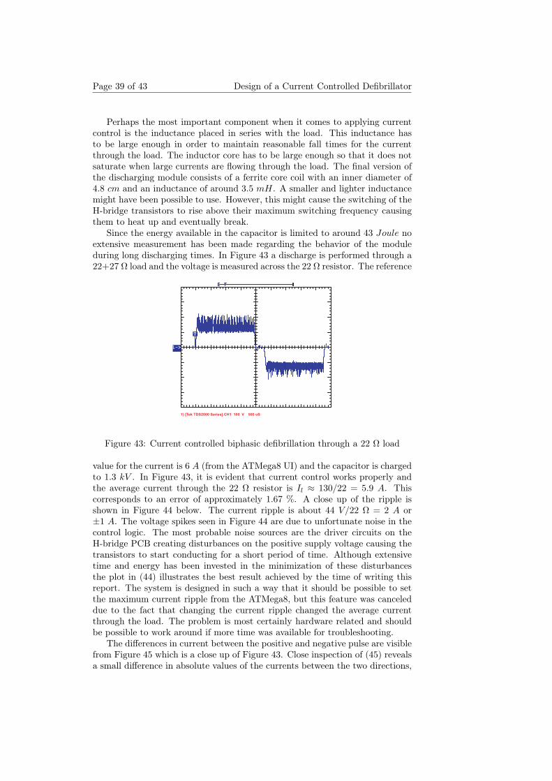
Page 39 of 43 Design of a Current Controlled Defibrillator
Perhaps the most important component when it comes to applying currentcontrol is the inductance placed in series with the load. This inductance hasto be large enough in order to maintain reasonable fall times for the currentthrough the load. The inductor core has to be large enough so that it does notsaturate when large currents are flowing through the load. The final version ofthe discharging module consists of a ferrite core coil with an inner diameter of4.8 cm and an inductance of around 3.5 mH. A smaller and lighter inductancemight have been possible to use. However, this might cause the switching of theH-bridge transistors to rise above their maximum switching frequency causingthem to heat up and eventually break.
Since the energy available in the capacitor is limited to around 43 Joule noextensive measurement has been made regarding the behavior of the moduleduring long discharging times. In Figure 43 a discharge is performed through a22+27 Ω load and the voltage is measured across the 22 Ω resistor. The reference
T
1->
1) [Tek TDS2000 Series].CH1 100 V 500 uS
Figure 43: Current controlled biphasic defibrillation through a 22 Ω load
value for the current is 6 A (from the ATMega8 UI) and the capacitor is chargedto 1.3 kV . In Figure 43, it is evident that current control works properly andthe average current through the 22 Ω resistor is Il ≈ 130/22 = 5.9 A. Thiscorresponds to an error of approximately 1.67 %. A close up of the ripple isshown in Figure 44 below. The current ripple is about 44 V/22 Ω = 2 A or±1 A. The voltage spikes seen in Figure 44 are due to unfortunate noise in thecontrol logic. The most probable noise sources are the driver circuits on theH-bridge PCB creating disturbances on the positive supply voltage causing thetransistors to start conducting for a short period of time. Although extensivetime and energy has been invested in the minimization of these disturbancesthe plot in (44) illustrates the best result achieved by the time of writing thisreport. The system is designed in such a way that it should be possible to setthe maximum current ripple from the ATMega8, but this feature was canceleddue to the fact that changing the current ripple changed the average currentthrough the load. The problem is most certainly hardware related and shouldbe possible to work around if more time was available for troubleshooting.
The differences in current between the positive and negative pulse are visiblefrom Figure 45 which is a close up of Figure 43. Close inspection of (45) revealsa small difference in absolute values of the currents between the two directions,
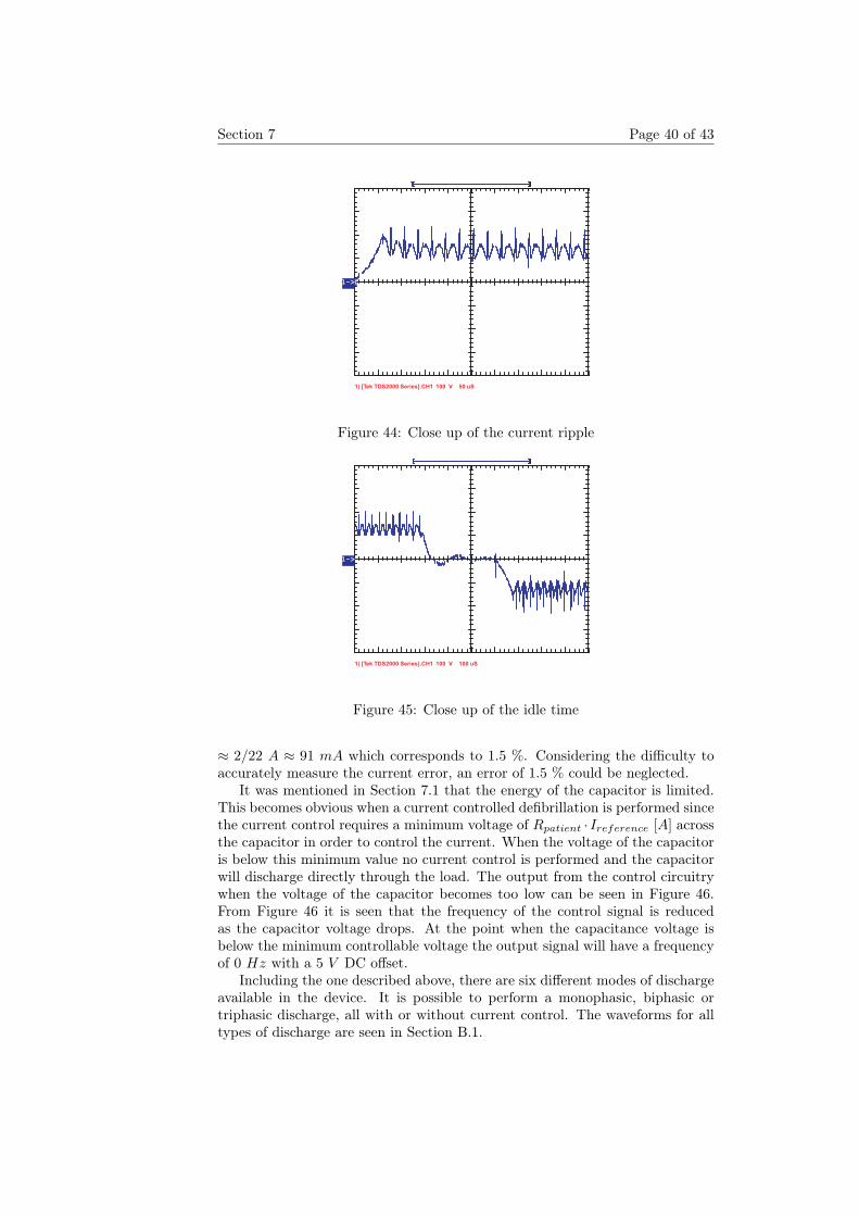
Section 7 Page 40 of 43
T1->
1) [Tek TDS2000 Series].CH1 100 V 50 uS
Figure 44: Close up of the current ripple
1->
1) [Tek TDS2000 Series].CH1 100 V 100 uS
Figure 45: Close up of the idle time
≈ 2/22 A ≈ 91 mA which corresponds to 1.5 %. Considering the difficulty toaccurately measure the current error, an error of 1.5 % could be neglected.
It was mentioned in Section 7.1 that the energy of the capacitor is limited.This becomes obvious when a current controlled defibrillation is performed sincethe current control requires a minimum voltage of Rpatient · Ireference [A] acrossthe capacitor in order to control the current. When the voltage of the capacitoris below this minimum value no current control is performed and the capacitorwill discharge directly through the load. The output from the control circuitrywhen the voltage of the capacitor becomes too low can be seen in Figure 46.From Figure 46 it is seen that the frequency of the control signal is reducedas the capacitor voltage drops. At the point when the capacitance voltage isbelow the minimum controllable voltage the output signal will have a frequencyof 0 Hz with a 5 V DC offset.
Including the one described above, there are six different modes of dischargeavailable in the device. It is possible to perform a monophasic, biphasic ortriphasic discharge, all with or without current control. The waveforms for alltypes of discharge are seen in Section B.1.
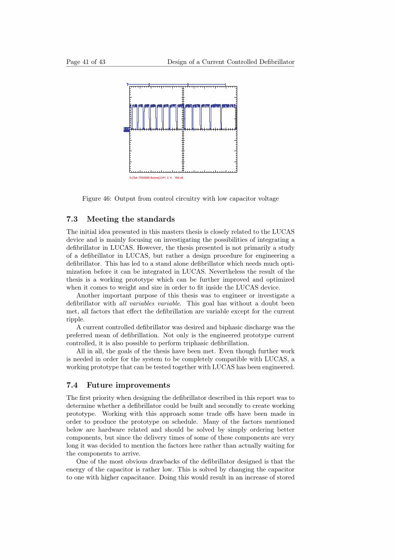
Page 41 of 43 Design of a Current Controlled Defibrillator
1->
3) [Tek TDS2000 Series].CH1 2 V 100 uS
Figure 46: Output from control circuitry with low capacitor voltage
7.3 Meeting the standardsThe initial idea presented in this masters thesis is closely related to the LUCASdevice and is mainly focusing on investigating the possibilities of integrating adefibrillator in LUCAS. However, the thesis presented is not primarily a studyof a defibrillator in LUCAS, but rather a design procedure for engineering adefibrillator. This has led to a stand alone defibrillator which needs much opti-mization before it can be integrated in LUCAS. Nevertheless the result of thethesis is a working prototype which can be further improved and optimizedwhen it comes to weight and size in order to fit inside the LUCAS device.
Another important purpose of this thesis was to engineer or investigate adefibrillator with all variables variable. This goal has without a doubt beenmet, all factors that effect the defibrillation are variable except for the currentripple.
A current controlled defibrillator was desired and biphasic discharge was thepreferred mean of defibrillation. Not only is the engineered prototype currentcontrolled, it is also possible to perform triphasic defibrillation.
All in all, the goals of the thesis have been met. Even though further workis needed in order for the system to be completely compatible with LUCAS, aworking prototype that can be tested together with LUCAS has been engineered.
7.4 Future improvementsThe first priority when designing the defibrillator described in this report was todetermine whether a defibrillator could be built and secondly to create workingprototype. Working with this approach some trade offs have been made inorder to produce the prototype on schedule. Many of the factors mentionedbelow are hardware related and should be solved by simply ordering bettercomponents, but since the delivery times of some of these components are verylong it was decided to mention the factors here rather than actually waiting forthe components to arrive.
One of the most obvious drawbacks of the defibrillator designed is that theenergy of the capacitor is rather low. This is solved by changing the capacitorto one with higher capacitance. Doing this would result in an increase of stored
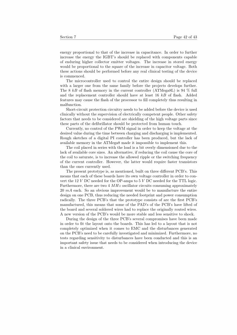
Section 7 Page 42 of 43
energy proportional to that of the increase in capacitance. In order to furtherincrease the energy the IGBT’s should be replaced with components capableof enduring higher collector emitter voltages. The increase in stored energywould be proportional to the square of the increase in capacitor voltage. Boththese actions should be performed before any real clinical testing of the deviceis commenced.
The microcontroller used to control the entire design should be replacedwith a larger one from the same family before the projects develops further.The 8 kB of flash memory in the current controller (ATMega8L) is 94 % fulland the replacement controller should have at least 16 kB of flash. Addedfeatures may cause the flash of the processor to fill completely thus resulting inmalfunction.
Short-circuit protection circuitry needs to be added before the device is usedclinically without the supervision of electrically competent people. Other safetyfactors that needs to be considered are shielding of the high voltage parts sincethese parts of the defibrillator should be protected from human touch.
Currently, no control of the PWM signal in order to keep the voltage at thedesired value during the time between charging and discharging is implemented.Rough sketches of a digital PI controller has been produced, but the lack ofavailable memory in the ATMega8 made it impossible to implement this.
The coil placed in series with the load is a bit overly dimensioned due to thelack of available core sizes. An alternative, if reducing the coil cause the core ofthe coil to saturate, is to increase the allowed ripple or the switching frequencyof the current controller. However, the latter would require faster transistorsthan the ones currently used.
The present prototype is, as mentioned, built on three different PCB’s. Thismeans that each of these boards have its own voltage controller in order to con-vert the 12 V DC needed for the OP-amps to 5 V DC needed for the TTL logic.Furthermore, there are two 4 MHz oscillator circuits consuming approximately20 mA each. So an obvious improvement would be to manufacture the entiredesign on one PCB, thus reducing the needed footprint and power consumptionradically. The three PCB’s that the prototype consists of are the first PCB’smanufactured, this means that some of the PAD’s of the PCB’s have lifted ofthe board and several soldered wires had to replace the originally routed wires.A new version of the PCB’s would be more stable and less sensitive to shock.
During the design of the three PCB’s several compromises have been madein order to fit the layout onto the boards. This has led to a layout that is notcompletely optimized when it comes to EMC and the disturbances generatedon the PCB’s need to be carefully investigated and minimized. Furthermore, notests regarding sensitivity to disturbances have been conducted and this is animportant safety issue that needs to be considered when introducing the devicein a clinical environment.
Page 43 of 43 Design of a Current Controlled Defibrillator
References[1] Agnvall, Clas G., Analog Elektronik, Kompendium 2000, department of
applied electronics, Lund Institute of Technology
[2] M. Olsson and M. Alaküla, Elmaskinsystem, IEA/LTH Lund, 2002
[3] Bardy, et al., 1996
[4] Cheng, David K., Field and Wave Electromagnetics, Addison Wesley, 1989,Second Edition
[5] ELFA, catalogue ELFA 51,2003
[6] Per Karlsson, Kraftelektronik, IEA/LTH Lund, Oct. 1998
[7] Per Karlsson, Power Electronics Laboratory Exercises, department of In-dustrial Electrical Engineering and Automation, Lund Institute of Tech-nology
[8] Studies presented by Lombardi, Gallagher, & Gennis, 1994
[9] J. W. Machin, J. Brownhill and A Furness, Design for a Constant PeakCurrent Defibrillator, IEEE transactions on biomedical engineering, Vol.37, No 7, July 1990
[10] Mohan N., Underland T., Robbins W., Power Electronics, Converters, Ap-plications, and Design, John Wiley & Sons Inc, 1995, Second Editon
[11] Zhang Y, Ramabadran RS, Boddicker KA, Bawaney I, Davies LR, Zim-merman MB, Wuthrich S, Jones JL, Kerber RE., Triphasic waveforms aresuperior to biphasic waveforms for transthoracic defibrillation: experimen-tal studies, J Am Coll Cardiol. 2003 Aug 6;42(3):568-75

Page i of xxxi Design of a Current Controlled Defibrillator
A Technical specifications
A.1 PortsThe table below describes some of the ports available to the user.
InputsType Value Description
When set to GND,Ext trig GND, 5 V discharge will com-
mence+Vcc +12 V Positive supply−Vcc −12 V Negative supply
A.2 ButtonsThe table below describes the buttons on the defibrillator.
ButtonsName Description
+ Menu button ’+’- Menu button ’-’
Enter Menu button ’enter’Cancel Menu button ’cancel’Reset Resets the processor
OV reset Resets the over voltage protec-tion circuit
Note: pressing the reset button may set some of the outputs undefined thuscausing malfunction
A.3 Current consumptionThe following table presents the current consumption of the system during dif-ferent stages. Note that currents listed are all avarage currents and the peakconsumption could be as high as 5 A momentarily.
Current consumptionMode CurrentIdle 90 mA
Charging max 0.6 ACharging min 0.3 A
Safety discharge 190 mA
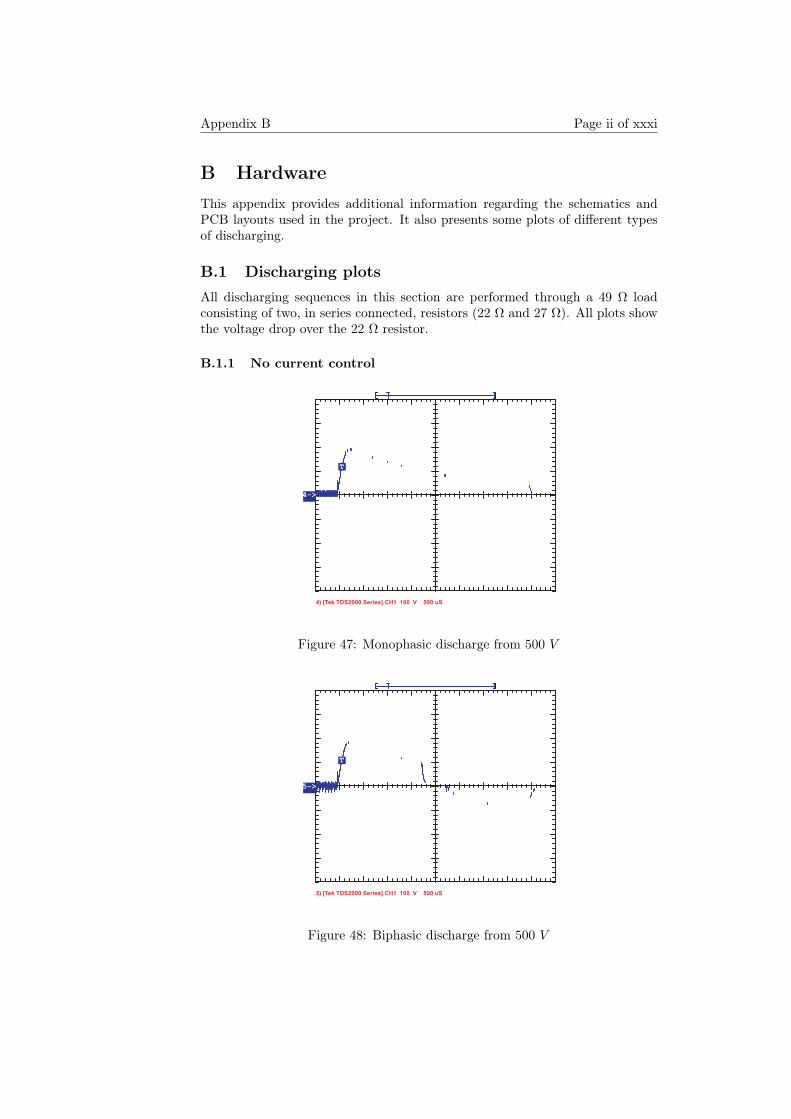
Appendix B Page ii of xxxi
B HardwareThis appendix provides additional information regarding the schematics andPCB layouts used in the project. It also presents some plots of different typesof discharging.
B.1 Discharging plotsAll discharging sequences in this section are performed through a 49 Ω loadconsisting of two, in series connected, resistors (22 Ω and 27 Ω). All plots showthe voltage drop over the 22 Ω resistor.
B.1.1 No current control
T
4->
4) [Tek TDS2000 Series].CH1 100 V 500 uS
Figure 47: Monophasic discharge from 500 V
T
5->
5) [Tek TDS2000 Series].CH1 100 V 500 uS
Figure 48: Biphasic discharge from 500 V
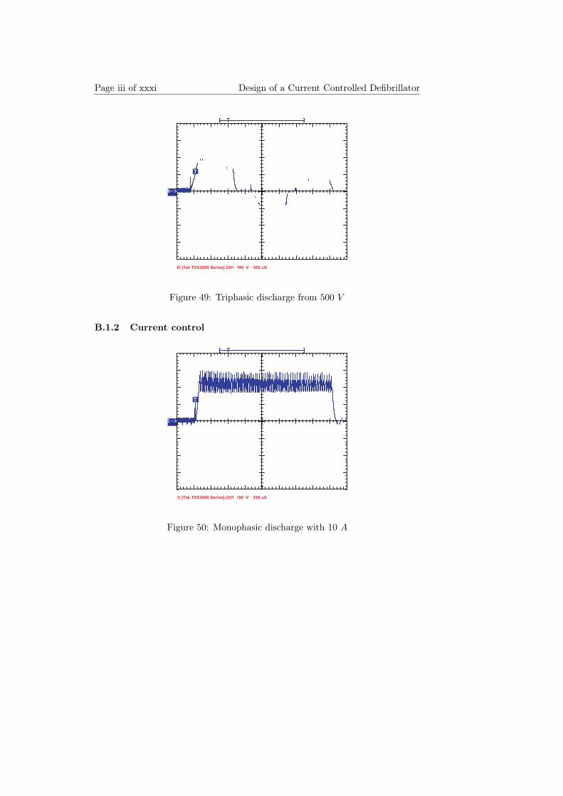
Page iii of xxxi Design of a Current Controlled Defibrillator
T
6->
6) [Tek TDS2000 Series].CH1 100 V 500 uS
Figure 49: Triphasic discharge from 500 V
B.1.2 Current control
T
1->
1) [Tek TDS2000 Series].CH1 100 V 250 uS
Figure 50: Monophasic discharge with 10 A
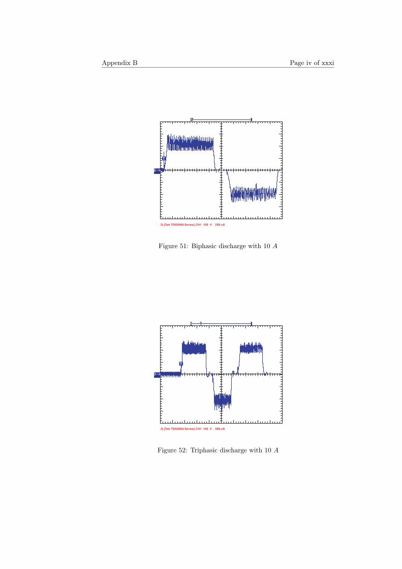
Appendix B Page iv of xxxi
T
2->
2) [Tek TDS2000 Series].CH1 100 V 250 uS
Figure 51: Biphasic discharge with 10 A
T
3->
3) [Tek TDS2000 Series].CH1 100 V 500 uS
Figure 52: Triphasic discharge with 10 A
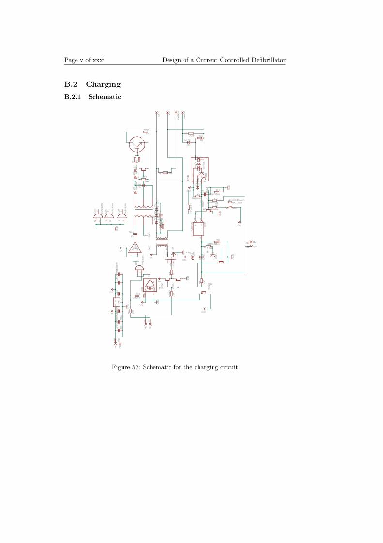
Page v of xxxi Design of a Current Controlled Defibrillator
B.2 ChargingB.2.1 Schematic
Figure 53: Schematic for the charging circuit
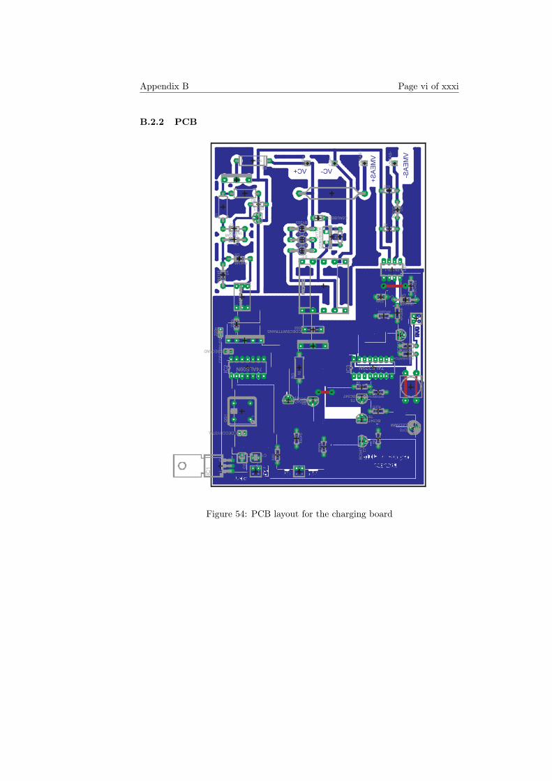
Appendix B Page vi of xxxi
B.2.2 PCB
Figure 54: PCB layout for the charging board
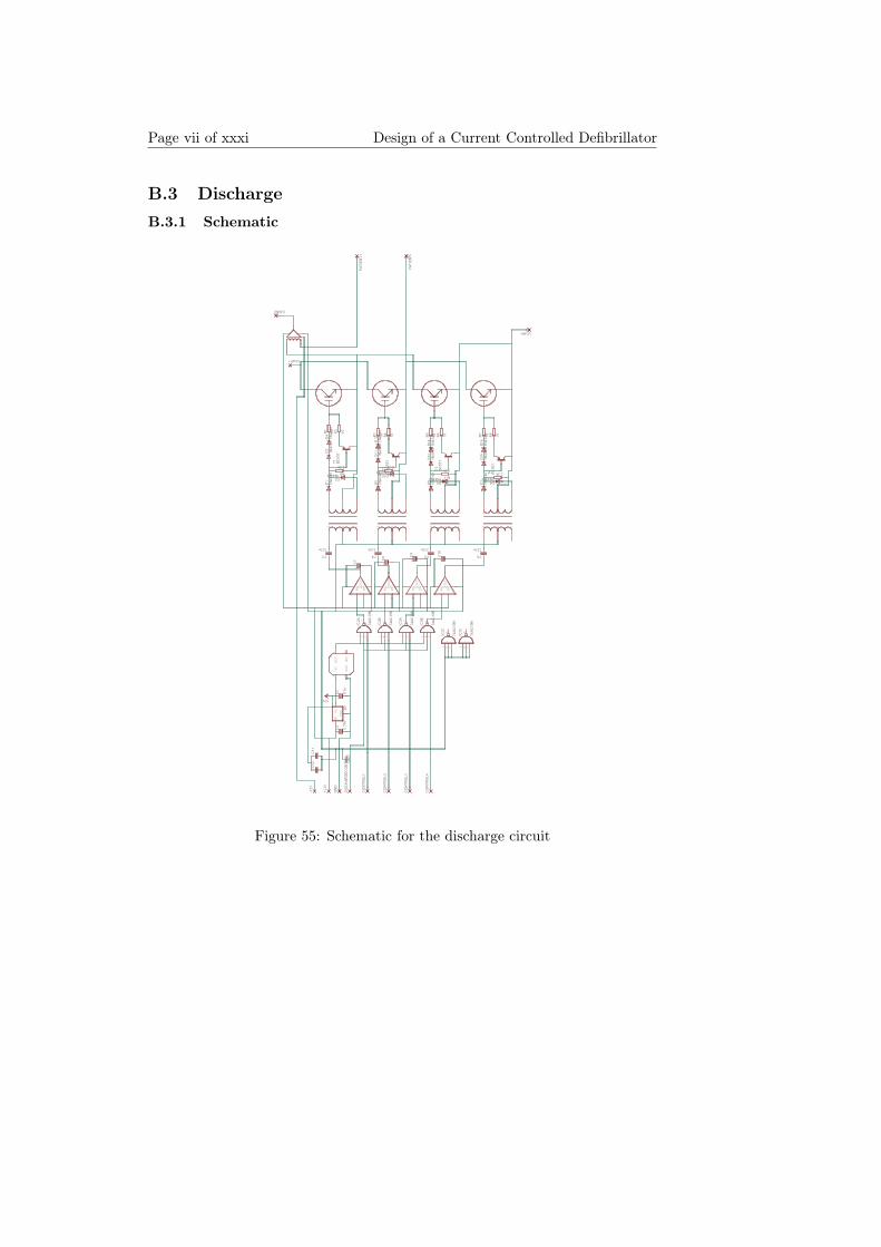
Page vii of xxxi Design of a Current Controlled Defibrillator
B.3 DischargeB.3.1 Schematic
Figure 55: Schematic for the discharge circuit
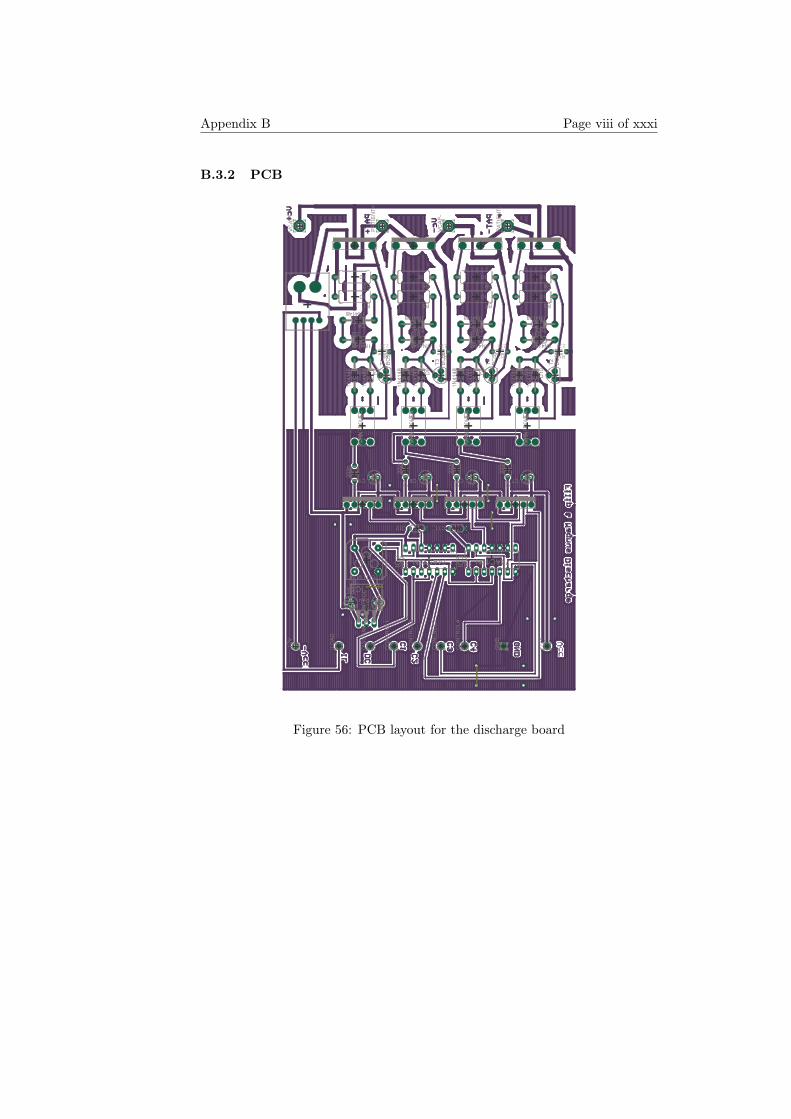
Appendix B Page viii of xxxi
B.3.2 PCB
Figure 56: PCB layout for the discharge board
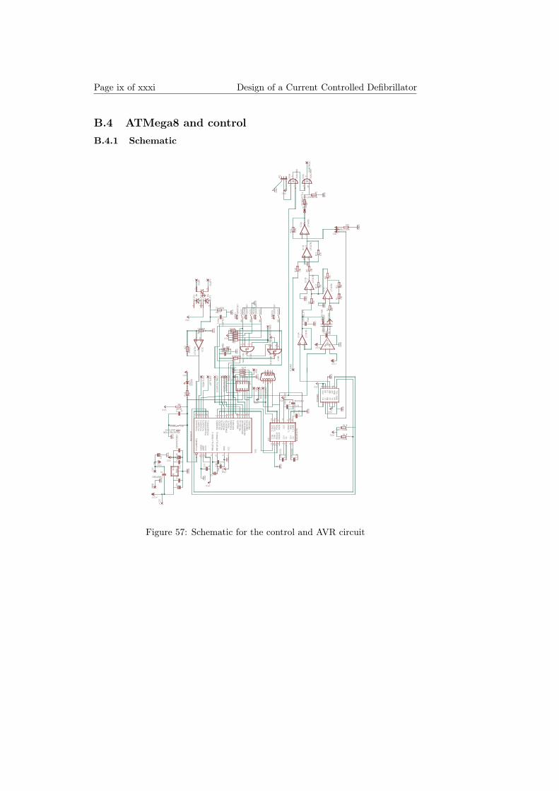
Page ix of xxxi Design of a Current Controlled Defibrillator
B.4 ATMega8 and controlB.4.1 Schematic
Figure 57: Schematic for the control and AVR circuit
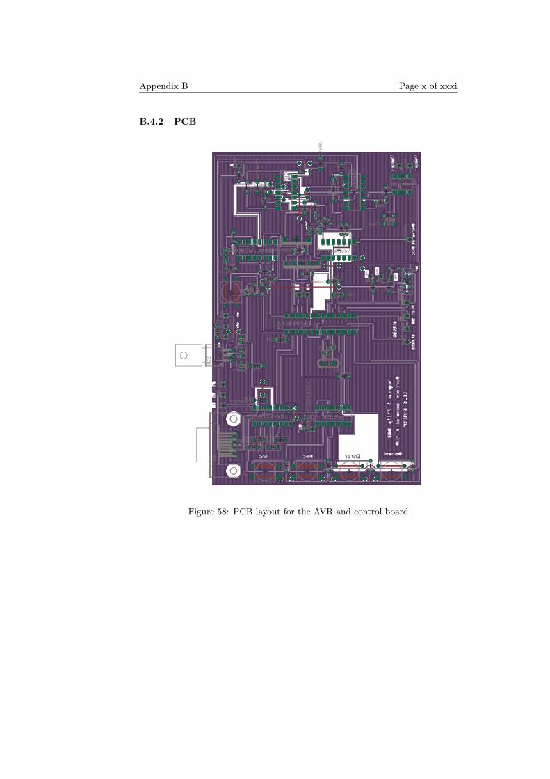
Appendix B Page x of xxxi
B.4.2 PCB
Figure 58: PCB layout for the AVR and control board
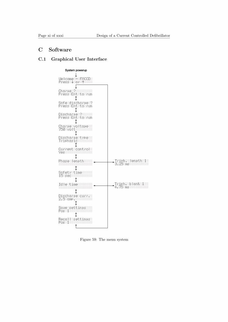
Page xi of xxxi Design of a Current Controlled Defibrillator
C Software
C.1 Graphical User Interface
System powerupSystem powerup
Figure 59: The menu system

Appendix C Page xii of xxxi
C.2 Program listing
The program listed below is compiled using ICCAVR20 from ImageCraft. Thissoftware environment enables the programmer to develop C programs and down-loaded the compiled code to the AVR directly from within ICCAVR.
// This is the complete source code file for FMCCD// (Filip Magnus Current Control Defibrillator)// It has support for both a small display// as well terminal program connected to the// serial port of a PC. The input to the program// is always buttons on the defibrillator, but// it is also possible to receive commands from// the serially connected PC.// The PC option is switched on via compiler directives.
// The source code is written to fit an ATMega8L running// at 4.0 MHz. If the crystal is changed, the source code// needs to be modified as well.
#include <iom8v.h>#include <macros.h>#include <Stdlib.h>#include <eeprom.h>#include "FMCCD.h"
// This first passage is to describe what should be// connected to the AVR//// What should be connected to the AVR when it comes// to Ports, PWMs, ADCs etc//// --- PORTB ---#define DDRPortB 0xFE// PBO (Pin 14) Connected to decrease (-) button (input)// PB1 (Pin 15) Connected to overvoltage reset// PB2 (Pin 16) Connected to Safety Discharge// PB3 (Pin 17) Connected to PWM charge (OC2)// PB4 (Pin 18) Extra option (a diode shows the current charge status)// PB5 (Pin 19) Extra option (a diode shows the current charge status)// PB6 (Pin 9) Used by XTAL// PB7 (Pin 10) Used by XTAL//// --- PORTD ---#define DDRPortD 0x02// PD0 (Pin 2) RXD (Input)// PD1 (Pin 3) TXD// PD2 (Pin 4) INT0 Connected to buttons and external def. request// PD3 (Pin 5) INT1 IRQ from overvoltage protection circuit// PD4 (Pin 6)// PD5 (Pin 11) Connected to Enter button (Input)// PD6 (Pin 12) Connected to Cancel button (Input)// PD7 (Pin 13) Connected to inc (+) button (Input)//// --- PORTC ---#define DDRPortC 0xFE// PC0 (Pin 23) Connected to measurement of sec voltage (ADC 0)// PC1 (Pin 24) Connected to IGBT 2 and 3 (Right leg)// PC2 (Pin 25) Connected to IGBT 1 and 4 (Left leg)// PC3 (Pin 26) Enable. Connected to transistor to alter reference value polarity// This signal is also used in the XOR circuity to alter// the output signal that is used as enable from the current control// PC4 (Pin 27) SDA// PC5 (Pin 28) SCL// PC6 (Pin 1 ) RESET
// First some defines
// Is display of terminal program used ?// If UseTerminalProg is used it is presumed that there is// a terminal program running on the PC and that the serial// port is attached to the device.
//#define UseTerminalProg#define UseSerialDisplay
// Input device used// If a PC is connected to the serial device this define// should be on// #define UsePCAsInputControl
// IGBT connections#define CIGBTLeftLeg 0x04#define CIGBTRightLeg 0x02#define CIGBTLeftLegPort PORTC#define CIGBTRightLegPort PORTC
20version 6.29
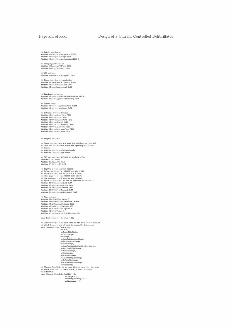
Page xiii of xxxi Design of a Current Controlled Defibrillator
// Safety discharge#define CSafetyDischargePort PORTB#define CSafetyDischarge 0x04#define CSafetyDischargeLowLevelADC 0
// Charging PWM define#define CChargingPWMPort OCR2#define CChargingPWMOff 0xFF
// ADC defines#define CSecondaryVoltageADC 0x00
// Diode for charge completion#define CDiodeCompletionPort PORTB#define CDiodeCompletionA 0x10#define CDiodeCompletionB 0x20
// Discharge polarity#define CDischargeWantedPolarityPort PORTC#define CDischargeWantedPolarity 0x08
// Overvoltage#define COvervoltageResetPort PORTB#define COvervoltageReset 0x02
// External button defines#define CButtonEnterPort PIND#define CButtonEnter 0x20#define CButtonCancelPort PIND#define CButtonCancel 0x40#define CButtonIncreasePort PIND#define CButtonIncrease 0x80#define CButtonDecreasePort PINB#define CButtonDecrease 0x01
// Program defines
// These two defines are used for calibrating the ADC// This has to be done since the optocoupler is not// linear// #define CalibrateVoltageLevels// #define TestVoltageLevels
// TWI defines not defined in include files#define START 0x08#define MT_SLA_ACK 0x18#define MT_DATA_ACK 0x28
// Digital potentiometer DS1803// Selection bits for DS1803 are the 4 MSB// which are defined as 0b0101 i.e.0x50// (See page 4 of the DS1803 data sheet)// The consequtive 3 bits is the address// which is defined (by us) in hardware to be 0b111#define DS1803_AdressRead 0x5F#define DS1803_AdressWrite 0x5E#define DS1803_Pot0Command 0xA9#define DS1803_Pot1Command 0xAA#define DS1803_Pot0and1Command 0xAF
// Misc defines#define CMaxNoOfUserBanks 6#define CEEPromDataValidMarker 0x4519#define CMaxChargingVoltage 1350#define CMinChargingVoltage 150#define CMinimumBlankingTime 1#define CHysterValue 5#define CTicsToQuarterMilliSeconds 124
enum Bool false = 0, true = 1;
// TProcessStep is an enum used in the main state machine// which keeps track of what is currently happeningenum TProcessStep psStartup,
psIdle,psEnterIdleState,psInitCharge,psCharge,psInitMaintenanceCharge,psMaintenanceCharge,psStopCharge,psInitForHumanControlledDischarge,psWaitingToDischarge,psPreDischarge,psDischarge,psStopDischarge,psInitSafetyDischarge,psSafetyDischarge,psStopSafetyDischarge,psShutDown;
// TCurrentMenuMode is an enum that is used for the menu// state machine. It keeps track of what is shown// currentlyenum TCurrentMenuMode mmIdle = 1,
mmCharge = 2,mmSafetyDischarge = 3,mmDischarge = 4,

Appendix C Page xiv of xxxi
mmSetChargingVoltage = 5,mmSetDischargeType = 6,mmCurrentControlled = 7,mmSetPhaseLength = 8,mmSetSafetyTime = 9,mmSetBlankingTime = 10,mmSetDischargeRefVoltage = 11,mmSaveParamToEEProm = 12,mmRestoreParamFromEEProm = 13,
// The menu modes below are used// for sub menu settings
mmSetPhaseLength_Mono1 = 14,mmSetPhaseLength_Bi1 = 15,mmSetPhaseLength_Bi2 = 16,mmSetPhaseLength_Tri1 = 17,mmSetPhaseLength_Tri2 = 18,mmSetPhaseLength_Tri3 = 19,mmSetBlankingTime_Bi = 20,mmSetBlankingTime_Tri1 = 21,mmSetBlankingTime_Tri2 = 22;
// These constants are used for the calibrated ADC// in order to convert an ADC value to a voltage level.// There is also a PWM lookup table. The intention// with this table is that a known voltage will be// kept with this PWM value#define LookupSize 23const unsigned int ADCLookup[LookupSize] = 7, 16, 57, 110, 172, 243, 314, 354, 394, 435, 472, 518, 560, 609,
652, 700, 745, 796, 842, 895, 940, 895, 1022;const unsigned int VoltageLookup[LookupSize] = 60, 100, 200, 300, 400, 500, 600, 650, 700, 750, 800, 850, 900, 950,
1000, 1050, 1100, 1150, 1200, 1250, 1300, 1350, 1400;const unsigned int PWMLookup[LookupSize] = 254, 254, 253, 250, 244, 242, 240, 239, 238, 238, 237, 237, 236, 235,
235, 234, 233, 232, 229, 222, 218, 215, 215;
// For showing a status (via a led) for the userenum TDiodeStatus dsLedOff = 1,
dsLedColor1 = 2,dsLedColor2 = 3;
enum TParamStoragePos psCurrentValue = 0,psOldValue = 1;
// All editable parameters are stored in this vector.// The reason for this is that is easy to revert to an old// value if the user decides to press Cancel during an editing// processint ParameterStorage[2][mmSetBlankingTime_Tri2 + 1];// Menu texts. These are stored in flash memory only// and are not copied to SRAM by the compilerconst char *MenuFirstLineText[] = "",
"Welcome - FMCCD","Charge ?","Safe discharge ?","Discharge ?","Charge voltage","Discharge type","Current control","Phase length","Safety time","Idle time","Discharge curr.","Save settings","Recall settings","Monophasic len.","Biph. length 1","Biph. length 2","Triph. length 1","Triph. length 2","Triph. length 3","Biph. blank","Triph. blank 1","Triph. blank 2","";
// TDischargeType is an enum describing what kind of// discharge that will be performed. Single is equal to// a monophasic, Double is a bipashic, Triple is tripahisc// dischargeenum TDischargeType dtSingle = 1,
dtDouble = 2,dtTriple = 3;
// TIGBTSequence describes which IGBT leg (that is which// pair of IBGT transistors) that is switched onenum TIGBTSequence ig_LeftLegOn,
ig_RightLegOn,ig_LegsOff;
// TDischargeWantedPolarity describes which polarity the// reference signal the controller should work with.enum TDischargeWantedPolarity wpPositive,
wpNegative;// TTWIAction describes what action that should take place// on the TwoWireInterface buss.enum TTWIAction TWI_StartCommand,
TWI_SlaveAddress,TWI_SlaveData,TWI_StopCommand;
// TDischargeParameter desribes which digital potentiometer// that should be used. dpWantedValue controls the// reference voltage for the controller and dpHysteresis

Page xv of xxxi Design of a Current Controlled Defibrillator
// controls the hysteresis voltage for the controller.enum TDischargeParameter dpWantedValue = 1,
dpHysteresis = 2;#ifdef UseSerialDisplay
// TDisplayControlCodes is an enum which describes control// codes for the display.enum TDisplayControlCodes dcClearScreen = 1,
dcMoveCursorHome = 2,dcInvisibleCursor = 12,dcBlinkingBlockCursor = 13,dcMoveCursorOneLeft = 16,dcMoveCursorOneRight = 20,dcMoveToFirstLine = 128,dcMoveToSecondLine = 192;
enum TDisplayCustomChars ccCursorUp = 3,ccCursorDown = 4;
#endif
// Some variable definitionsunsigned char MaintenacePWM = 248;#ifdef CalibrateVoltageLevels
unsigned char CurrCalibPWMValue;#endif#ifdef TestVoltageLevels
unsigned char CurrCalibPWMValue;#endif
// Buffer used for printingchar PrintStrBuff[20];
unsigned char CurrentProcessStep = psStartup;unsigned char CurrentMenuMode = mmIdle;unsigned char EditingCurrentParameter = false;unsigned char NbrOfOvervoltageIRQ = 0;unsigned char IgnoreOverVoltageIRQ = true;unsigned char OkeyToShowMenu = true;int SafetyDischargeCounter = 0;
//signed long Ik; // This is used for the integral part of the PI-reg
// Initialize default values to paramterersvoid InitializeParameterStorage()
ParameterStorage[psCurrentValue][mmSetChargingVoltage] = CMinChargingVoltage;ParameterStorage[psCurrentValue][mmSetDischargeType] = dtDouble;ParameterStorage[psCurrentValue][mmCurrentControlled] = true;ParameterStorage[psCurrentValue][mmSetSafetyTime] = 15;ParameterStorage[psCurrentValue][mmSetBlankingTime] = 200;ParameterStorage[psCurrentValue][mmSetDischargeRefVoltage] = 25;ParameterStorage[psCurrentValue][mmSaveParamToEEProm] = 1;ParameterStorage[psCurrentValue][mmRestoreParamFromEEProm] = 1;ParameterStorage[psCurrentValue][mmSetPhaseLength_Mono1] = 20;ParameterStorage[psCurrentValue][mmSetPhaseLength_Bi1] = 20;ParameterStorage[psCurrentValue][mmSetPhaseLength_Bi2] = 20;ParameterStorage[psCurrentValue][mmSetPhaseLength_Tri1] = 20;ParameterStorage[psCurrentValue][mmSetPhaseLength_Tri2] = 20;ParameterStorage[psCurrentValue][mmSetPhaseLength_Tri3] = 20;ParameterStorage[psCurrentValue][mmSetBlankingTime_Bi] = 2;ParameterStorage[psCurrentValue][mmSetBlankingTime_Tri1] = 2;ParameterStorage[psCurrentValue][mmSetBlankingTime_Tri2] = 2;
// Initialise the IO portsvoid port_init(void)
DDRB = DDRPortB;PORTB = 0x00;
DDRC = DDRPortC;PORTC = 0x00;
DDRD = DDRPortD;PORTD = 0x00;
//TWI (I2C) initialisationvoid twi_init(void)
TWCR= 0X00; //disable twiTWBR= 0x03; //set bit rateTWSR= 0x03; //set prescaleTWAR= 0x00; //set slave addressTWCR= 0x45; //enable twi
// UART0 initialisation// Baud rate: 9600,8 bit, no parityvoid uart0_init(void)
UCSRB = 0x00; //disable while setting baud rateUCSRA = 0x00;UCSRC = 0x86;UBRRL = 0x19; //set baud rate lo
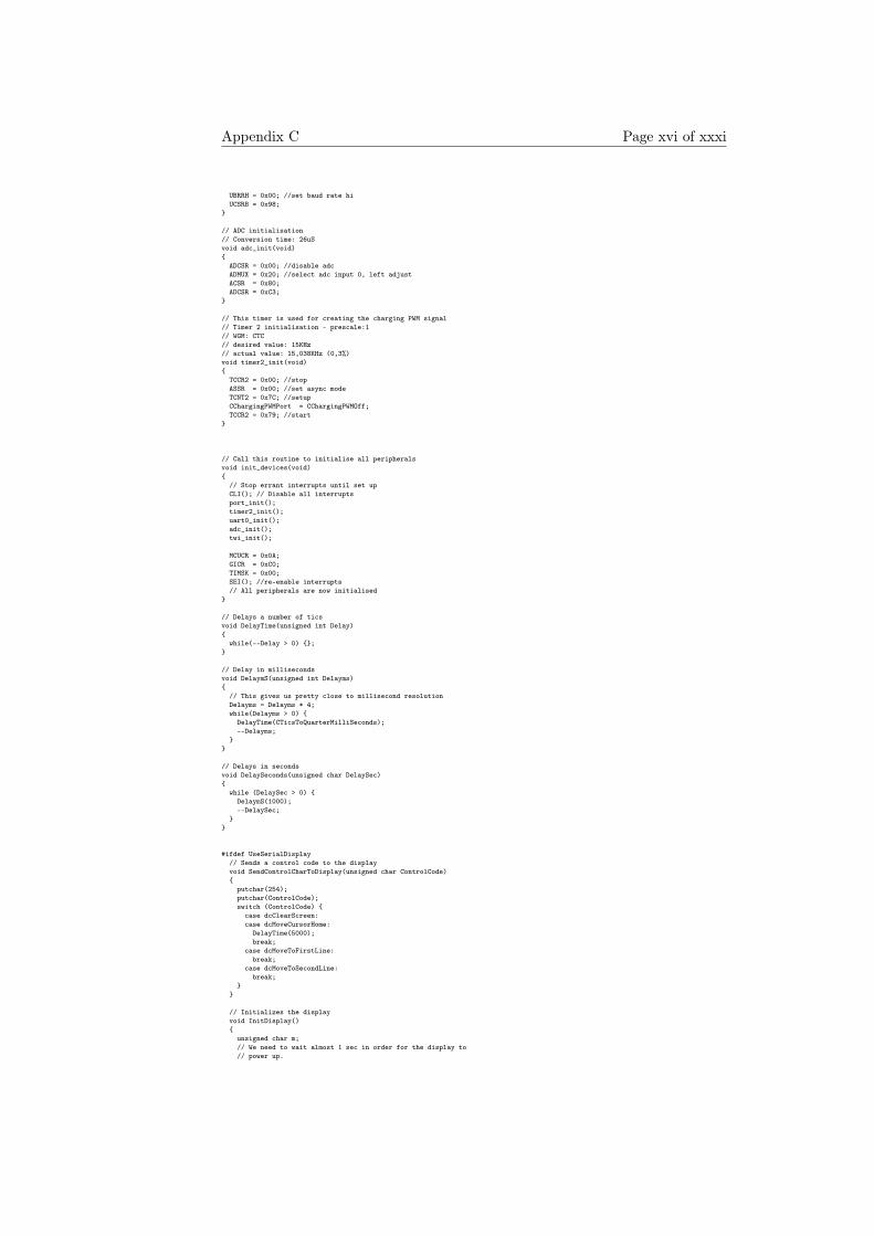
Appendix C Page xvi of xxxi
UBRRH = 0x00; //set baud rate hiUCSRB = 0x98;
// ADC initialisation// Conversion time: 26uSvoid adc_init(void)
ADCSR = 0x00; //disable adcADMUX = 0x20; //select adc input 0, left adjustACSR = 0x80;ADCSR = 0xC3;
// This timer is used for creating the charging PWM signal// Timer 2 initialisation - prescale:1// WGM: CTC// desired value: 15KHz// actual value: 15,038KHz (0,3%)void timer2_init(void)
TCCR2 = 0x00; //stopASSR = 0x00; //set async modeTCNT2 = 0x7C; //setupCChargingPWMPort = CChargingPWMOff;TCCR2 = 0x79; //start
// Call this routine to initialise all peripheralsvoid init_devices(void)
// Stop errant interrupts until set upCLI(); // Disable all interruptsport_init();timer2_init();uart0_init();adc_init();twi_init();
MCUCR = 0x0A;GICR = 0xC0;TIMSK = 0x00;SEI(); //re-enable interrupts// All peripherals are now initialised
// Delays a number of ticsvoid DelayTime(unsigned int Delay)
while(--Delay > 0) ;
// Delay in millisecondsvoid DelaymS(unsigned int Delayms)
// This gives us pretty close to millisecond resolutionDelayms = Delayms * 4;while(Delayms > 0)
DelayTime(CTicsToQuarterMilliSeconds);--Delayms;
// Delays in secondsvoid DelaySeconds(unsigned char DelaySec)
while (DelaySec > 0) DelaymS(1000);--DelaySec;
#ifdef UseSerialDisplay// Sends a control code to the displayvoid SendControlCharToDisplay(unsigned char ControlCode)
putchar(254);putchar(ControlCode);switch (ControlCode)
case dcClearScreen:case dcMoveCursorHome:
DelayTime(5000);break;
case dcMoveToFirstLine:break;
case dcMoveToSecondLine:break;
// Initializes the displayvoid InitDisplay()
unsigned char m;// We need to wait almost 1 sec in order for the display to// power up.
Page xvii of xxxi Design of a Current Controlled Defibrillator
DelaymS(900);// We want to make character 0 (position 80 in the display// RAM) enmpty. This enables us to use the puts function// which terminates with a carriage return that shows up// as character 0putchar(254); // Tell display toputchar(80); // point to RAM (ASCII code 2)for (m = 0; m < 8; m++)
putchar(0);// Then design an up and down arrow for showing that// it is possible to edit the current value// First the up arrorputchar(254); // Tell display toputchar(88); // point to RAM (ASCII code 3)putchar(4); // Dataputchar(14); // Dataputchar(21); // Datafor (m = 0; m < 5; m++)
putchar(4); // Dataputchar(254); // Tell display toputchar(96); // point to RAM (ASCII code 4)for (m = 0; m < 5; m++)
putchar(4); // Dataputchar(21); // Dataputchar(14); // Dataputchar(4); // Dataputchar(254); // Tell display toputchar(128); // move cursor back to screen
// We override the normal library routine sine// it prints a CR in the end which looks bad on// our displayint puts(char *s)
while (*s != ’\0’) putchar (*s);s++;
#endif
// This routine writes data to the serial portvoid WriteDataToScreen(char s[])
puts(s);
// This method writes data that resides only in flashvoid WriteConstDataToScreen(const char s[])
char pTempChar[] = "1234567890123456";// We need to copy the const declared string from flash to a// RAM variable in order to be able to print it outstrcpy(pTempChar, MenuFirstLineText[CurrentMenuMode]);WriteDataToScreen(pTempChar);
// This method shows an error message and then enters an endless// loop preventing the system from running again until system resetvoid ErrorHalt(char Msg1[], char Msg2[])
SendControlCharToDisplay(dcClearScreen);WriteDataToScreen(Msg1);SendControlCharToDisplay(dcMoveToSecondLine);WriteDataToScreen(Msg2);while (true);
// This method shows a user message and then waits for// two seconds before continuingvoid WriteDelayedUserMessage(char Msg1[], char Msg2[])
SendControlCharToDisplay(dcClearScreen);WriteDataToScreen(Msg1);SendControlCharToDisplay(dcMoveToSecondLine);WriteDataToScreen(Msg2);DelaySeconds(2);
// This routine writes data to the serial portvoid WriteIntToScreen(char PreStr[], int Value, char PostStr[])
// First the leading stringchar m;if (PreStr != NULL)
for (m = 0; PreStr[m] != ’\0’; m++)putchar (PreStr[m]);
// Then check if this is a negative number// (itoa will print -10 as 65526 if an int)if (Value < 0)
Value = abs(Value);
Appendix C Page xviii of xxxi
putchar(’-’);
// Write the value to serial portitoa(PrintStrBuff, Value, 10);puts(PrintStrBuff);
if (PostStr != NULL) for (m = 0; PostStr[m] != ’\0’; m++)
putchar (PostStr[m]);
// This method is used for notifying the user of the current// status. Two ports are used to either light a green or a// red diodevoid SetDiodeStatus(unsigned char Status)
switch (Status) case dsLedOff:
CDiodeCompletionPort = CDiodeCompletionPort & ~CDiodeCompletionA;CDiodeCompletionPort = CDiodeCompletionPort & ~CDiodeCompletionB;break;
case dsLedColor1:CDiodeCompletionPort = CDiodeCompletionPort | CDiodeCompletionA;CDiodeCompletionPort = CDiodeCompletionPort & ~CDiodeCompletionB;break;
case dsLedColor2:CDiodeCompletionPort = CDiodeCompletionPort & ~CDiodeCompletionA;CDiodeCompletionPort = CDiodeCompletionPort | CDiodeCompletionB;break;
// This method saves all parameters to EEProm so that// the user later can recall them if so desiredvoid SaveParametersToEEProm(unsigned char BankNo)
// Each bank is 40 * 2 bytes big (i.e. 40 integers)// On the first address we store if the data is valid// If a specific value found, data is valid
// Since BankNo is a value from 1 to 6// we reserve the space below 32 for// future program usage// This leads us to the following (EEPROM is 512 bytes)// if the maximal bankno is 6 :// (6 - 1) * 40 * 2 + 32 = 432// from 432 to 512 there is exactly 80 bytes to save for the last bankint Address = (BankNo - 1) * 40 * 2 + 32;unsigned char M;int CheckValue = CEEPromDataValidMarker;EEPROM_WRITE(Address, CheckValue);Address += sizeof(int);for (M = mmSetChargingVoltage; M <= mmSetBlankingTime_Tri2; M++)
EEPROM_WRITE(Address, ParameterStorage[psCurrentValue][M]);Address += sizeof(int);
// This method recalls all parameters from EEProm.// This is also done at power up if the contents of the// EEProm is validvoid RestoreParametersFromEEProm(unsigned char BankNo)
// Each bank is 40 * 2 bytes big (i.e. 40 integers)// On the first address we store if the data is valid// If a specific value found, data is valid
// Since BankNo is a value from 1 to 6// we reserve the space below 32 for// future program usage// This leads us to the following (EEPROM is 512 bytes)// if the maximal bankno is 6 :// (6 - 1) * 40 * 2 + 32 = 432// from 432 to 512 there is exactly 80 bytes to save for the last bankint Address = (BankNo - 1) * 40 * 2 + 32;unsigned char M;int CheckValue;EEPROM_READ(Address, CheckValue);Address += sizeof(int);if (CheckValue == CEEPromDataValidMarker)
for (M = mmSetChargingVoltage; M <= mmSetBlankingTime_Tri2; M++) EEPROM_READ(Address, ParameterStorage[psCurrentValue][M]);Address += sizeof(int);
else
ParameterStorage[psCurrentValue][mmSetChargingVoltage] = CMinChargingVoltage - 50;
// This method converts the inparameter to a time// ms (the value is supposed to be shifted left by 2)// which gives it a 0.25 resolutionvoid ConvertTimeToMilliSecondsAndPrint(int Time)
// Time is here a value that has two decimals,// i.e. it is of fixed point type.

Page xix of xxxi Design of a Current Controlled Defibrillator
unsigned char Temp = 0;WriteIntToScreen(NULL, Time >> 2, ".");if ((Time & 0x01) == 0x01)
Temp = 25;if ((Time & 0x02) == 0x02)
Temp += 50;WriteIntToScreen(NULL, Temp, " ms");
// Shows the main menuvoid ShowMenu()
if (OkeyToShowMenu) SendControlCharToDisplay(dcClearScreen);WriteConstDataToScreen(MenuFirstLineText[CurrentMenuMode]);SendControlCharToDisplay(dcMoveToSecondLine);
switch (CurrentMenuMode) case mmIdle:
WriteDataToScreen("Press ");putchar(ccCursorUp);WriteDataToScreen(" or ");putchar(ccCursorDown);break;
case mmDischarge:case mmCharge:case mmSafetyDischarge:
WriteDataToScreen("Press Ent to run");break;
case mmSetChargingVoltage:WriteIntToScreen(NULL, ParameterStorage[psCurrentValue][CurrentMenuMode], " volt");break;
case mmSetDischargeType:switch (ParameterStorage[psCurrentValue][CurrentMenuMode])
case dtSingle:WriteDataToScreen("Monophasic");break;
case dtDouble:WriteDataToScreen("Biphasic");break;
case dtTriple:WriteDataToScreen("Triphasic");break;
break;
case mmCurrentControlled:if (ParameterStorage[psCurrentValue][CurrentMenuMode])
WriteDataToScreen("Yes");else
WriteDataToScreen("No");break;
case mmSetPhaseLength:case mmSetBlankingTime:
// Do nothing. This menu contains a submenubreak;
case mmSetSafetyTime:WriteIntToScreen(NULL, ParameterStorage[psCurrentValue][CurrentMenuMode], " sec");break;
case mmSetPhaseLength_Mono1:case mmSetPhaseLength_Bi1:case mmSetPhaseLength_Bi2:case mmSetPhaseLength_Tri1:case mmSetPhaseLength_Tri2:case mmSetPhaseLength_Tri3:case mmSetBlankingTime_Bi:case mmSetBlankingTime_Tri1:case mmSetBlankingTime_Tri2:
ConvertTimeToMilliSecondsAndPrint(ParameterStorage[psCurrentValue][CurrentMenuMode]);break;
case mmSetDischargeRefVoltage:WriteIntToScreen(NULL, ParameterStorage[psCurrentValue][CurrentMenuMode] / 10, ".");WriteIntToScreen(NULL, ParameterStorage[psCurrentValue][CurrentMenuMode] % 10, " amp.");break;
case mmSaveParamToEEProm:case mmRestoreParamFromEEProm:
WriteIntToScreen("Pos ", ParameterStorage[psCurrentValue][CurrentMenuMode], NULL);break;
default:break;
if (EditingCurrentParameter)
putchar(32);putchar(ccCursorUp);putchar(ccCursorDown);SendControlCharToDisplay(dcBlinkingBlockCursor);
elseSendControlCharToDisplay(dcInvisibleCursor);
// Edit a settings depending on the current menu

Appendix C Page xx of xxxi
// The inparameter describes which way (up or down)// that we a re goingvoid AlterSetting(unsigned char ButtonPressed)
// First find out which direction we are going. Up or down ?signed char Dir = (ButtonPressed == wpPositive) ? 1 : -1;unsigned char TempChar;switch (CurrentMenuMode)
// These are parameters that are adjustablecase mmSetChargingVoltage:
ParameterStorage[psCurrentValue][CurrentMenuMode] += Dir * 50;if (ParameterStorage[psCurrentValue][CurrentMenuMode] < CMinChargingVoltage)
ParameterStorage[psCurrentValue][CurrentMenuMode] = CMinChargingVoltage;if (ParameterStorage[psCurrentValue][CurrentMenuMode] > CMaxChargingVoltage)
ParameterStorage[psCurrentValue][CurrentMenuMode] = CMaxChargingVoltage;break;
case mmSetDischargeType:ParameterStorage[psCurrentValue][CurrentMenuMode] += Dir;if (ParameterStorage[psCurrentValue][CurrentMenuMode] < dtSingle)
ParameterStorage[psCurrentValue][CurrentMenuMode] = dtTriple;else if (ParameterStorage[psCurrentValue][CurrentMenuMode] > dtTriple)
ParameterStorage[psCurrentValue][CurrentMenuMode] = dtSingle;break;
case mmCurrentControlled:if (ParameterStorage[psCurrentValue][CurrentMenuMode])
ParameterStorage[psCurrentValue][CurrentMenuMode] = false;else
ParameterStorage[psCurrentValue][CurrentMenuMode] = true;// Make sure that the digital potentiometer is set correctlySetCurrentDischargingParameters();break;
case mmSetPhaseLength_Mono1:case mmSetPhaseLength_Bi1:case mmSetPhaseLength_Bi2:case mmSetPhaseLength_Tri1:case mmSetPhaseLength_Tri2:case mmSetPhaseLength_Tri3:
ParameterStorage[psCurrentValue][CurrentMenuMode] += Dir;if (ParameterStorage[psCurrentValue][CurrentMenuMode] < 0)
ParameterStorage[psCurrentValue][CurrentMenuMode] = 0;break;
case mmSetBlankingTime_Bi:case mmSetBlankingTime_Tri1:case mmSetBlankingTime_Tri2:
ParameterStorage[psCurrentValue][CurrentMenuMode] += Dir;if (ParameterStorage[psCurrentValue][CurrentMenuMode] < CMinimumBlankingTime)
ParameterStorage[psCurrentValue][CurrentMenuMode] = CMinimumBlankingTime;break;
case mmSaveParamToEEProm:case mmRestoreParamFromEEProm:
ParameterStorage[psCurrentValue][CurrentMenuMode] += Dir;if (ParameterStorage[psCurrentValue][CurrentMenuMode] > CMaxNoOfUserBanks)
ParameterStorage[psCurrentValue][CurrentMenuMode] = 1;if (ParameterStorage[psCurrentValue][CurrentMenuMode] < 1)
ParameterStorage[psCurrentValue][CurrentMenuMode] = CMaxNoOfUserBanks;break;
case mmSetSafetyTime:ParameterStorage[psCurrentValue][CurrentMenuMode] += Dir;
if (ParameterStorage[psCurrentValue][CurrentMenuMode] < 1)ParameterStorage[psCurrentValue][CurrentMenuMode] = 1;
break;
case mmSetDischargeRefVoltage:// The user is about to change the value of the digital// potentiometers. We will address the DS1803 chip right// away to reflect the change !// If we fail, we will set the current value to zero in order// to show that something went wrong...ParameterStorage[psCurrentValue][CurrentMenuMode] += Dir * 5;if (ParameterStorage[psCurrentValue][CurrentMenuMode] > 250)
ParameterStorage[psCurrentValue][CurrentMenuMode] = 250;if (ParameterStorage[psCurrentValue][CurrentMenuMode] < 10)
ParameterStorage[psCurrentValue][CurrentMenuMode] = 10;if (!SetDischargingParameter(dpWantedValue, ParameterStorage[psCurrentValue][CurrentMenuMode]))
ParameterStorage[psCurrentValue][CurrentMenuMode] = 0;break;
default:break;
// This method sets both the digital potentiometers to// the value determined by the menu system.boolean SetCurrentDischargingParameters()
boolean Result = false;unsigned char TempDischargeSetting;
// Do the user want a current controlled def. ? If not

Page xxi of xxxi Design of a Current Controlled Defibrillator
// we set the wanted value (the ref voltage) to 0xFFif (ParameterStorage[psCurrentValue][mmCurrentControlled])
TempDischargeSetting = ParameterStorage[psCurrentValue][mmSetDischargeRefVoltage];else
TempDischargeSetting = 0xFF;
// Make sure that the digital potentiometers have the correct valueResult = SetDischargingParameter(dpHysteresis, CHysterValue);if (Result)
Result = SetDischargingParameter(dpWantedValue, TempDischargeSetting);return Result;
// This method sets the wipers (used to set// a predefined voltage level to the discharge// logic) to a value from 0 to 255.// Param is the parameter (i.e. the wiper)// that is to be changed// Value is the wanted output setting, a value// from 0 to 255.boolean SetDischargingParameter(unsigned char Param,
unsigned char Value)
boolean Result = false;switch (Param)
case dpWantedValue:Result = WriteToDS1803(DS1803_Pot0Command, Value);break;
case dpHysteresis:Result = WriteToDS1803(DS1803_Pot1Command, Value);break;
return Result;
// This method sets an IO port to control if the wanted// value (reference voltage to the summator) should be// negative or positive. The IO signal is fed to a// PNP transistor.void SetDischargeWantedPolarity(unsigned char Pol)
if (Pol == wpPositive)CDischargeWantedPolarityPort = CDischargeWantedPolarityPort | CDischargeWantedPolarity;
else if (Pol == wpNegative)CDischargeWantedPolarityPort = CDischargeWantedPolarityPort & ~CDischargeWantedPolarity;
// Sends a reset signal to the overvoltage circuitvoid ResetOvervoltageCircuit()
COvervoltageResetPort = COvervoltageResetPort | COvervoltageReset;DelayTime(500);COvervoltageResetPort = COvervoltageResetPort & ~COvervoltageReset;
// This method does all the setting of IO signals// in order to do a proper dischargevoid DoDischarge()
CLI();switch (ParameterStorage[psCurrentValue][mmSetDischargeType])
case dtSingle:// Set the IO signal for the tolerance band regulatorSetDischargeWantedPolarity(wpNegative);// Switch on one leg of IGBT transistorsEnableIGBTLeg(ig_RightLegOn);// Let the pulse last for a the desired timeDelayTime(CTicsToQuarterMilliSeconds * ParameterStorage[psCurrentValue][mmSetPhaseLength_Mono1]);// Switch off the IGBT legEnableIGBTLeg(ig_LegsOff);break;
case dtDouble:SetDischargeWantedPolarity(wpNegative);EnableIGBTLeg(ig_RightLegOn);DelayTime(CTicsToQuarterMilliSeconds * ParameterStorage[psCurrentValue][mmSetPhaseLength_Bi1]);EnableIGBTLeg(ig_LegsOff);// Change the polarity for the tolerance band regulatorSetDischargeWantedPolarity(wpPositive);// Wait for the specified blanking timeDelayTime(CTicsToQuarterMilliSeconds * ParameterStorage[psCurrentValue][mmSetBlankingTime_Bi]);EnableIGBTLeg(ig_LeftLegOn);DelayTime(CTicsToQuarterMilliSeconds * ParameterStorage[psCurrentValue][mmSetPhaseLength_Bi2]);EnableIGBTLeg(ig_LegsOff);break;
case dtTriple:SetDischargeWantedPolarity(wpNegative);EnableIGBTLeg(ig_RightLegOn);DelayTime(CTicsToQuarterMilliSeconds * ParameterStorage[psCurrentValue][mmSetPhaseLength_Tri1]);EnableIGBTLeg(ig_LegsOff);SetDischargeWantedPolarity(wpPositive);DelayTime(CTicsToQuarterMilliSeconds * ParameterStorage[psCurrentValue][mmSetBlankingTime_Tri1]);EnableIGBTLeg(ig_LeftLegOn);DelayTime(CTicsToQuarterMilliSeconds * ParameterStorage[psCurrentValue][mmSetPhaseLength_Tri2]);EnableIGBTLeg(ig_LegsOff);
Appendix C Page xxii of xxxi
// Change the polarity for the tolerance band regulator back againSetDischargeWantedPolarity(wpNegative);// Wait for the specified blanking time againDelayTime(CTicsToQuarterMilliSeconds * ParameterStorage[psCurrentValue][mmSetBlankingTime_Tri2]);EnableIGBTLeg(ig_RightLegOn);DelayTime(CTicsToQuarterMilliSeconds * ParameterStorage[psCurrentValue][mmSetPhaseLength_Tri3]);EnableIGBTLeg(ig_LegsOff);break;
default:break;
SEI();
// This method does the actual setting// of the IO signal to switch on and off// the IGBT transistors
// The physical layout of the IGBTs are as// follows//// 1 2// X// 3 4//// LeftLeg diagonal is 1 and 4// RightLeg diagonal is 2 and 3//void EnableIGBTLeg(unsigned char IGBTLeg)
switch (IGBTLeg) case ig_LeftLegOn:
CIGBTRightLegPort = CIGBTRightLegPort & ~CIGBTRightLeg;CIGBTLeftLegPort = CIGBTLeftLegPort | CIGBTLeftLeg;break;
case ig_RightLegOn:CIGBTLeftLegPort = CIGBTLeftLegPort & ~CIGBTLeftLeg;CIGBTRightLegPort = CIGBTRightLegPort | CIGBTRightLeg;break;
case ig_LegsOff:CIGBTRightLegPort = CIGBTRightLegPort & ~CIGBTRightLeg;CIGBTLeftLegPort = CIGBTLeftLegPort & ~CIGBTLeftLeg;break;
default:break;
// Get an ADC reading from the selected ADCunsigned int GetADCValue(unsigned char ADCNumber)
int Value;ADMUX = ADCNumber;ADCSRA = ADCSRA | 0x40; // Start ADCwhile ((ADCSRA & 0x40) == 0x40); // wait for ADC to finnishValue = ADCL;Value += ((ADCH << 8));return Value;
// This method determines if the cap contains any energy, or rather// can we see any voltage residing in the cap...boolean IsCapacitorCharged()
return (GetADCValue(CSecondaryVoltageADC) > CSafetyDischargeLowLevelADC);
// This method performs an ADC measurement// and returns the calculated voltageunsigned int MeasureVoltage()
return CalcVoltage(GetADCValue(CSecondaryVoltageADC));
// Method that calclates the current voltage// as a function of the ADC valueunsigned int CalcVoltage(unsigned int ADCValue)
// This method contains two versions of code.// First one that does a coarse but fast// linear approximation.// Then one version which has certain fixpoints// that the code linearises between
// Version 1// This is the short version that is not very exact//return (ADCValue * 2) + 350;
// Version 2// This is the long version with a lookuptable// Unfortunately it is also a bit slower
Page xxiii of xxxi Design of a Current Controlled Defibrillator
int Cnt;
Cnt = 0;// First iterate through the ADC table to find out where we arewhile ((Cnt <= LookupSize) && (ADCValue >= ADCLookup[Cnt]))
++Cnt;--Cnt;// If we are ’above’ the table, calc with the last known valueif (Cnt == LookupSize)
return ((ADCValue - ADCLookup[LookupSize - 2]) * 2 + VoltageLookup[LookupSize - 2]);// If we are below, just return zero voltageif (Cnt == -1)
return 0;// Otherwise return the calulated value in the tablereturn ((ADCValue - ADCLookup[Cnt]) * 2 + VoltageLookup[Cnt]);
// This method returns a PWM value for the inparameter (in volts)// so that the voltage over the CAP can be made constantunsigned char GetPWMForCurrentVoltage(unsigned int CurrentVoltage)
// Since we do not measure the current through the transformers// primary side we have a lookup table that gives us a reasonable// duty cycle depending on the current voltage
int Cnt;Cnt = 0;// First iterate through the Voltage table to find out where we arewhile ((Cnt <= LookupSize) && (CurrentVoltage >= VoltageLookup[Cnt]))
++Cnt;--Cnt;// If we are ’above’ the table, just return the last known valueif (Cnt == LookupSize)
return PWMLookup[LookupSize - 2];// If we are below, just return the lowest valueif (Cnt == -1)
return PWMLookup[0];// Otherwise just return the PWM value for the current spanreturn PWMLookup[Cnt];
// This method writes a wiper setting to the Dallas / Maxim// potentiometer IC. The communication is handled over the// I2C (TwoWireInterface) protocol.boolean WriteToDS1803(unsigned char PotAddress, unsigned char Value)
// First send a start commandboolean Result = TWICommunication(TWI_StartCommand, 0);// then send the slave identifier (hardcoded in the DS1803)if (Result)
Result = TWICommunication(TWI_SlaveAddress, DS1803_AdressWrite);// then send the address of the potentiometer to be used (0, 1 or both)if (Result)
Result = TWICommunication(TWI_SlaveData, PotAddress);// then send the actual potentiometer settingif (Result)
Result = TWICommunication(TWI_SlaveData, Value);// and finally send the stop commandif (Result)
Result = TWICommunication(TWI_StopCommand, 0);return Result;
// This method sends either a command or data over the I2C (TWI) buss.boolean TWICommunication(unsigned char Command, unsigned char Data)
boolean Result = true;switch (Command)
case TWI_StartCommand:TWCR = 0xA4;Result = WaitForTWIFlag();if (Result)Result = ((TWSR & 0xF8) == START);
break;
case TWI_SlaveAddress:case TWI_SlaveData:
TWDR = Data;TWCR = 0x84;Result = WaitForTWIFlag();if (Result)
if (Command == TWI_SlaveAddress)Result = ((TWSR & 0xF8) == MT_SLA_ACK);
elseResult = ((TWSR & 0xF8) == MT_DATA_ACK);
break;
case TWI_StopCommand:TWCR = 0x94;break;

Appendix C Page xxiv of xxxi
default:return false;
return Result;
boolean WaitForTWIFlag()
unsigned int LoopCounter = 0;// We will now wait for the TWI interrupt flag to be set// This is done by hardware when the current TWI operation// has finished. Note that we will not reset the flag since this// implies a new TWI operation.// We have a afety counter just in case the device does not// respondwhile (((TWCR & 0x80) == 0x00) && (LoopCounter < 5000))
++LoopCounter;return ((TWCR & 0x80) == 0x80);
// This method is called when we receive an// interrupt for incoming characters#pragma interrupt_handler uart0_rx_isr:12void uart0_rx_isr(void)
#ifdef UsePCAsInputControlswitch (UDR)
case ’q’:CurrentProcessStep = psEnterIdleState;break;
case ’w’:CurrentProcessStep = psInitCharge;break;
case ’e’:CurrentProcessStep = psInitSafetyDischarge;break;
case ’r’:CurrentProcessStep = psInitForHumanControlledDischarge;break;
// Below are things for debuggingcase ’a’:
SetDischargingParameter(dpWantedValue, 2);break;
case ’s’:SetDischargingParameter(dpWantedValue, 22);break;
case ’d’:SetDischargingParameter(dpWantedValue, 5);break;
case ’z’:EnableIGBTLeg(ig_LeftLegOn);break;
case ’x’:EnableIGBTLeg(ig_RightLegOn);break;
case ’c’:EnableIGBTLeg(ig_LegsOff);break;
case ’v’:SetDischargeWantedPolarity(wpPositive);break;
case ’b’:SetDischargeWantedPolarity(wpNegative);break;
default:break;
#endif
#pragma interrupt_handler twi_isr:18void twi_isr(void)
// We get an interrupt every time a TWI event is completed// However, we don’t use the interrupt currently due to the// fact that we are not doing multiple things while using// the TWI line. This implies that we are waiting for a flag// to be set by polling anyway and an interrupt driven scenario// would not give us any benefits.

Page xxv of xxxi Design of a Current Controlled Defibrillator
#pragma interrupt_handler int0_isr:2void int0_isr(void)
// Okay, so we have seen an interrupt// This could be due to a number of different reasons
// 1. A key has been pressed// All keys are wired so that when a key is pressed// an interrupt is sent. We then read the ports to// find out which key it was.//// 2. An external discharge signal was sent to us// This means that we should defibrillate. How do we know?// Well, we got an interrupt and none of the buttons were// pressed...
// First check the status of buttons//// Execute, Cancel, Increase and Decrease buttons
if ((CButtonEnterPort & CButtonEnter) == 0x00)
switch (CurrentProcessStep) case psCharge:
break;case psMaintenanceCharge:
// Discharge is the only thing we can doCurrentProcessStep = psInitForHumanControlledDischarge;break;
default:// Are we in a menu that requires immediate// action instead of changing a parameter ?switch (CurrentMenuMode)
case mmIdle:break;
case mmCharge:CurrentProcessStep = psInitCharge;break;
case mmSafetyDischarge:CurrentProcessStep = psInitSafetyDischarge;break;
case mmDischarge:CurrentProcessStep = psInitForHumanControlledDischarge;
break;
case mmSaveParamToEEProm:case mmRestoreParamFromEEProm:
if (EditingCurrentParameter) if (CurrentMenuMode == mmSaveParamToEEProm)
SaveParametersToEEProm(ParameterStorage[psCurrentValue][CurrentMenuMode]);else
InitializeParameterStorage();RestoreParametersFromEEProm(ParameterStorage[psCurrentValue][CurrentMenuMode]);
EditingCurrentParameter = false;
else EditingCurrentParameter = true;ParameterStorage[psOldValue][CurrentMenuMode] = ParameterStorage[psCurrentValue][CurrentMenuMode];
break;
case mmSetPhaseLength:// The user want to alter the length of the current// discharge type. Depending on which one that is selected// that sub menu will be displayed.switch (ParameterStorage[psCurrentValue][mmSetDischargeType])
case dtSingle:CurrentMenuMode = mmSetPhaseLength_Mono1;break;
case dtDouble:CurrentMenuMode = mmSetPhaseLength_Bi1;break;
case dtTriple:CurrentMenuMode = mmSetPhaseLength_Tri1;break;
break;
case mmSetBlankingTime:// The user want to alter the blanking time for the current// discharge type. Depending on which one that is selected// that sub menu will be displayed.switch (ParameterStorage[psCurrentValue][mmSetDischargeType])
case dtSingle:// We can not set a banking time for a monophasic (single) pulsebreak;
case dtDouble:CurrentMenuMode = mmSetBlankingTime_Bi;break;
case dtTriple:CurrentMenuMode = mmSetBlankingTime_Tri1;break;
break;
default:// We are in a menu that has an editable

Appendix C Page xxvi of xxxi
// parameterEditingCurrentParameter = !EditingCurrentParameter;ParameterStorage[psOldValue][CurrentMenuMode] = ParameterStorage[psCurrentValue][CurrentMenuMode];break;
break;
else if ((CButtonCancelPort & CButtonCancel) == 0x00) // The user has pressed the cancel button. This either means// that we want to abandon the current editing process// or that we want to go back from the current submenu// to the main menu or cancel a charging process
// First check if we are in the process of charging// or maintenace charging the capacitor. If this is// the case we enter idle state, but we leave the// capacitor charged. This might be subject to change// later on...switch (CurrentProcessStep)
case psCharge:#ifdef CalibrateVoltageLevels
CChargingPWMPort = CChargingPWMOff;DelaySeconds(3);
#endifcase psMaintenanceCharge:
CurrentProcessStep = psStopCharge;break;
default:// If we are not editing a value and we are in a submenu,// Cancel means that we want to go up a menu levelif (!EditingCurrentParameter)
switch (CurrentMenuMode) case mmSetPhaseLength_Mono1:case mmSetPhaseLength_Bi1:case mmSetPhaseLength_Bi2:case mmSetPhaseLength_Tri1:case mmSetPhaseLength_Tri2:case mmSetPhaseLength_Tri3:
CurrentMenuMode = mmSetPhaseLength;break;
case mmSetBlankingTime_Bi:case mmSetBlankingTime_Tri1:case mmSetBlankingTime_Tri2:
CurrentMenuMode = mmSetBlankingTime;break;
else
// We were editing a value, and hence pressing Cancel// means that we want the old value back without// storing the newly edited oneParameterStorage[psCurrentValue][CurrentMenuMode] = ParameterStorage[psOldValue][CurrentMenuMode];
EditingCurrentParameter = false;break;
else if ((CButtonIncreasePort & CButtonIncrease) == 0x00) // The increase (+) button has been pressed.// This either means that we are editing a value or// that we are browsing the menu system. If we are// browsing the menu system we have to take special care// if we are in a submenu.
switch (CurrentProcessStep) case psMaintenanceCharge:case psCharge:
#ifdef CalibrateVoltageLevels++CurrCalibPWMValue;
#endif#ifdef TestVoltageLevels
++CurrCalibPWMValue;#endifbreak;
default:if (EditingCurrentParameter)
AlterSetting(wpPositive);else
// Okay, we are not editing a value. Are we in a submenu?// The submenus have different ’length’ so we must take this// into account.switch (CurrentMenuMode)
case mmSetPhaseLength_Mono1:break;
case mmSetPhaseLength_Bi1:CurrentMenuMode = mmSetPhaseLength_Bi2;break;
case mmSetPhaseLength_Bi2:CurrentMenuMode = mmSetPhaseLength_Bi1;break;
case mmSetPhaseLength_Tri1:case mmSetPhaseLength_Tri2:
++CurrentMenuMode;break;
case mmSetPhaseLength_Tri3:CurrentMenuMode = mmSetPhaseLength_Tri1;break;
case mmSetBlankingTime_Bi:break;
Page xxvii of xxxi Design of a Current Controlled Defibrillator
case mmSetBlankingTime_Tri1:CurrentMenuMode = mmSetBlankingTime_Tri2;break;
case mmSetBlankingTime_Tri2:CurrentMenuMode = mmSetBlankingTime_Tri1;break;
default:// Okay, we were not in a submenu. Just iterate// around in the top level menu system then as usual.++CurrentMenuMode;
// If we have a non current controlled option switched on// the current menu should not be visibleif ((!ParameterStorage[psCurrentValue][mmCurrentControlled]) &&
(CurrentMenuMode == mmSetDischargeRefVoltage))++CurrentMenuMode;
// If there is voltage in the CAP we should not be able// to change settings. Then we should just be allowed// to charge, discharge and safety dischargeif (IsCapacitorCharged() && (CurrentMenuMode > mmDischarge))
CurrentMenuMode = mmCharge;else if (CurrentMenuMode > mmRestoreParamFromEEProm)
CurrentMenuMode = mmCharge;break;
break;
else if ((CButtonDecreasePort & CButtonDecrease) == 0x00)
// The decrease (-) button has been pressed.// This either means that we are editing a value or// that we are browsing the menu system. If we are// browsing the menu system we have to take special care// if we are in a submenu.
switch (CurrentProcessStep) case psMaintenanceCharge:case psCharge:
#ifdef CalibrateVoltageLevels--CurrCalibPWMValue;
#endif#ifdef TestVoltageLevels
--CurrCalibPWMValue;#endifbreak;
default:if (EditingCurrentParameter)
AlterSetting(wpNegative);else
// Okay, we are not editing a value. Are we in a submenu?// The submenus have different ’length’ so we must take this// into account.switch (CurrentMenuMode)
case mmSetPhaseLength_Mono1:break;
case mmSetPhaseLength_Bi1:CurrentMenuMode = mmSetPhaseLength_Bi2;break;
case mmSetPhaseLength_Bi2:CurrentMenuMode = mmSetPhaseLength_Bi1;break;
case mmSetPhaseLength_Tri2:case mmSetPhaseLength_Tri3:
--CurrentMenuMode;break;
case mmSetPhaseLength_Tri1:CurrentMenuMode = mmSetPhaseLength_Tri3;break;
case mmSetBlankingTime_Bi:break;
case mmSetBlankingTime_Tri1:CurrentMenuMode = mmSetBlankingTime_Tri2;break;
case mmSetBlankingTime_Tri2:CurrentMenuMode = mmSetBlankingTime_Tri1;break;
default:// Okay, we were not in a submenu. Just iterate// around in the top level menu system then as usual.--CurrentMenuMode;
// If we have a non current controlled option switched on// the current menu should not be visibleif ((!ParameterStorage[psCurrentValue][mmCurrentControlled]) &&
(CurrentMenuMode == mmSetDischargeRefVoltage))--CurrentMenuMode;
// If there is voltage in the CAP we should not be able// to change settings. Then we should just be allowed// to charge, discharge and safety dischargeif (IsCapacitorCharged() && (CurrentMenuMode < mmCharge))
CurrentMenuMode = mmDischarge;else if (CurrentMenuMode < mmCharge)
CurrentMenuMode = mmRestoreParamFromEEProm;break;
break;
Appendix C Page xxviii of xxxi
else // We got ourselves an interrupt even though no key was// pressed...// This must be an external interrupt// The user wants to either charge or discharge// the cap
switch (CurrentProcessStep) case psIdle:
// We are in idle mode. An interrupt here means that// we want to charge the capacitorCurrentProcessStep = psInitCharge;break;
case psMaintenanceCharge:// We are currently in a charged mode. An interrupt here// means that we want to dischargeCurrentProcessStep = psPreDischarge;break;
default:
break;
ShowMenu();
#pragma interrupt_handler int1_isr:3void int1_isr(void)
// Okay, we have seen an interrupt// Reason is that we have an overvoltage from the overvoltage logic.
// We might get interrupts during power-up. We want to// avoid this from getting the system into a locked mode.if (!IgnoreOverVoltageIRQ)
// First stop the PWM pulseCChargingPWMPort = CChargingPWMOff;++NbrOfOvervoltageIRQ;// then start discharging if this is the first timeif (NbrOfOvervoltageIRQ == 1)
WriteDelayedUserMessage("Overvoltage err!", "Discharging");CurrentProcessStep = psStopCharge;
else CSafetyDischargePort = CSafetyDischargePort | CSafetyDischarge;ErrorHalt("OVERVOLTAGE ERR!", "System halted!");
// The intention with this code was to create a simple// PI controller which kept the voltage constant// It turns out however that the compiler creates much// larger code if the type long is used. Long was used// due to the fact that we need decent resolution// for our discrete time calculations.// We did not have time to solve this problem since// the code already takes up 94% of the available// flash memory/*
unsigned char PIReg(int CurrentCAPVoltage)
// We have a PI regulator that tries to keep the voltage// over the CAP constant.// Inparameter is the current voltage measured by the// ADC and the menu system supplies us with the wanted value
// The returned result from this method is a ’new’ PWM value
// This define tells us how many bits that should be used for// the decimal part and how many for the integer part// i.e. a long is 32 bits. We need// SignBit + IntegerBits + DecimalBits#define IntegerCutOffPos 10;
signed long VoltageErr;signed long uk;signed long a1; //(20 << IntegerCutOffPos);signed long a2; // = (10 << (IntegerCutOffPos - 3)); // Should be 0.010
// First calculate the errorVoltageErr = (CurrentCAPVoltage - ParameterStorage[psCurrentValue][mmSetChargingVoltage]);
// Calculate the new output : uk = a1*ek + Ik;uk = (a2); // >> IntegerCutOffPos) + Ik;
// then calculate a new integral part for the next run// Ik(+) = Ik + a2*e//Ik = Ik + (((a2 << IntegerCutOffPos) * VoltageErr) >> IntegerCutOffPos);
// The last thing we need to do is to rescale the output

Page xxix of xxxi Design of a Current Controlled Defibrillator
//return (uk >> IntegerCutOffPos);return 5;
*/
// Main methodvoid main(void)
unsigned int LoopCount = 0;unsigned char TempChar;int TempValue;int TempVoltage;int DischargeCounter = 0;
// First init all devicesIgnoreOverVoltageIRQ = true;init_devices();InitializeParameterStorage();
while(1 == 1)
LoopCount++;
switch (CurrentProcessStep) case psStartup:
#ifdef UseSerialDisplayInitDisplay();
#endif#ifdef UseTerminalProg
WriteDataToScreen("System initialised, version 0.1");#ifdef UsePCAsInputControl
WriteDataToScreen("Use keys:");WriteDataToScreen("q - Idle");WriteDataToScreen("w - Charge");WriteDataToScreen("e - Safety discharge");WriteDataToScreen("r - Discharge");
#endifWriteDataToScreen("");WriteDataToScreen("System idle");WriteDataToScreen("");
#endif
// In case the overvoltage reset happens to be switched on// during power up (spikes ?) we will just reset itResetOvervoltageCircuit();
// Get the settings from EEProm. The settings retreived are those// in position 1RestoreParametersFromEEProm(1);
// Initialize digital potentiometersSetCurrentDischargingParameters();
IgnoreOverVoltageIRQ = false;CurrentProcessStep = psEnterIdleState;break;
case psEnterIdleState:CChargingPWMPort = CChargingPWMOff;CSafetyDischargePort = CSafetyDischargePort & ~CSafetyDischarge;CurrentProcessStep = psIdle;OkeyToShowMenu = true;ShowMenu();SetDiodeStatus(dsLedOff);break;
case psIdle:// Do nothing right nowbreak;
case psInitCharge:OkeyToShowMenu = false;SetDiodeStatus(dsLedColor1);#ifdef UseTerminalProg
WriteIntToScreen("Upper voltage = ", ParameterStorage[psCurrentValue][mmSetChargingVoltage], NULL);WriteDataToScreen("Starting to charge...");
#endif#ifdef UseSerialDisplay
SendControlCharToDisplay(dcClearScreen);WriteIntToScreen("Charging to ", ParameterStorage[psCurrentValue][mmSetChargingVoltage], NULL);
#endif#ifdef CalibrateVoltageLevels
CurrCalibPWMValue = 255;#endif#ifdef TestVoltageLevels
CurrCalibPWMValue = 255;#endifCurrentProcessStep = psCharge;break;
case psCharge:// During the charging process we measure the voltage over the cap// and depending on that voltage we set different PWM values
#ifdef CalibrateVoltageLevelsTempValue = GetADCValue(CSecondaryVoltageADC);CChargingPWMPort = CurrCalibPWMValue;
#elseTempValue = MeasureVoltage();#ifdef TestVoltageLevels
CChargingPWMPort = CurrCalibPWMValue;

Appendix C Page xxx of xxxi
#elseif (TempValue < 800)
CChargingPWMPort = 216;else
CChargingPWMPort = 207;#endif
#endif
if (LoopCount % 1000 == 0) #ifdef UseTerminalProg
WriteIntToScreen("Voltage = ", TempValue, NULL);#endif#ifdef UseSerialDisplay
#ifdef CalibrateVoltageLevelsSendControlCharToDisplay(dcClearScreen);WriteIntToScreen("PWM : ", CurrCalibPWMValue, NULL);SendControlCharToDisplay(dcMoveToSecondLine);WriteIntToScreen("DAC : ", TempValue, " steps");
#else#ifdef TestVoltageLevels
SendControlCharToDisplay(dcClearScreen);WriteIntToScreen("ADC : ", GetADCValue(CSecondaryVoltageADC), NULL);
#endifSendControlCharToDisplay(dcMoveToSecondLine);WriteIntToScreen("Voltage : ", TempValue, " V ");
#endif#endif
if (TempValue > ParameterStorage[psCurrentValue][mmSetChargingVoltage])
CurrentProcessStep = psInitMaintenanceCharge;CurrentMenuMode = mmDischarge;
break;
case psInitMaintenanceCharge:SetDiodeStatus(dsLedColor2);CChargingPWMPort = GetPWMForCurrentVoltage(ParameterStorage[psCurrentValue][mmSetChargingVoltage]);SafetyDischargeCounter = ParameterStorage[psCurrentValue][mmSetSafetyTime];#ifdef UseTerminalProg
WriteDataToScreen("Maintenance charging...");#endifCurrentProcessStep = psMaintenanceCharge;break;
case psMaintenanceCharge:if (LoopCount % 1000 == 0)
TempVoltage = MeasureVoltage();// Check if we should safety dischargeif (LoopCount % 9000 == 0)
SafetyDischargeCounter--;#ifdef UseSerialDisplay
SendControlCharToDisplay(dcClearScreen);WriteConstDataToScreen(MenuFirstLineText[mmDischarge]);SendControlCharToDisplay(dcMoveToSecondLine);WriteIntToScreen("Ent in ", SafetyDischargeCounter, " secs");
#endif#ifdef UseTerminalProg
WriteIntToScreen("Safetycounter = ", SafetyDischargeCounter, BULL);#endifif (SafetyDischargeCounter == 0)
CurrentProcessStep = psStopCharge;break;
case psStopCharge:CChargingPWMPort = CChargingPWMOff;#ifdef UseTerminalProg
WriteDataToScreen("Charging stopped...");#endif#ifdef UseSerialDisplay
SendControlCharToDisplay(dcClearScreen);WriteDataToScreen("Charging stopped...");
#endifCurrentProcessStep = psInitSafetyDischarge;break;
case psInitSafetyDischarge:OkeyToShowMenu = false;#ifdef UseTerminalProg
WriteDataToScreen("Starting safety discharge...");#endif#ifdef UseSerialDisplay
SendControlCharToDisplay(dcClearScreen);WriteDataToScreen("Safety discharge");SendControlCharToDisplay(dcMoveToSecondLine);WriteDataToScreen("Please wait !");
#endifCSafetyDischargePort = CSafetyDischargePort | CSafetyDischarge;CurrentProcessStep = psSafetyDischarge;break;
case psSafetyDischarge:if (!IsCapacitorCharged())
CurrentProcessStep = psStopSafetyDischarge;break;
case psStopSafetyDischarge:// We wait some extra time just to be sure

Page xxxi of xxxi Design of a Current Controlled Defibrillator
DelaySeconds(2);CSafetyDischargePort = CSafetyDischargePort & ~CSafetyDischarge;#ifdef UseTerminalProg
WriteDataToScreen("Safety discharge done!");#endif#ifdef UseSerialDisplay
WriteDelayedUserMessage("Safety discharge", "Done !");#endifCurrentProcessStep = psEnterIdleState;break;
case psInitForHumanControlledDischarge:OkeyToShowMenu = false;#ifdef UseTerminalProg
WriteDataToScreen("Stand by for discharge");#endif#ifdef UseSerialDisplay
SendControlCharToDisplay(dcClearScreen);WriteDataToScreen("Discharging...");
#endifDischargeCounter = 2;CurrentProcessStep = psWaitingToDischarge;// This is due to the fact that the overvoltage circuit// might react during a discharge
case psWaitingToDischarge:if (LoopCount % 10000 == 0)
DischargeCounter--;#ifdef UseTerminalProg
WriteIntToScreen("Time to discharge = ", DischargeCounter, NULL);#endif#ifdef UseSerialDisplay
SendControlCharToDisplay(dcClearScreen);WriteDataToScreen("Discharging...");SendControlCharToDisplay(dcMoveToSecondLine);WriteIntToScreen("Wait... ", DischargeCounter, NULL);
#endifif (DischargeCounter == 0)
CurrentProcessStep = psPreDischarge;break;
case psPreDischarge:IgnoreOverVoltageIRQ = true;CChargingPWMPort = CChargingPWMOff;CurrentProcessStep = psDischarge;break;
case psDischarge:#ifdef UseTerminalProg
WriteDataToScreen("Discharging");#endifDoDischarge();CurrentProcessStep = psStopDischarge;break;
case psStopDischarge:#ifdef UseTerminalProgWriteDataToScreen("Discharging done");#endif
DelayTime(1000);ResetOvervoltageCircuit();
if (IsCapacitorCharged()) WriteDelayedUserMessage("Discharge done", "Now safety dis.");CurrentProcessStep = psInitSafetyDischarge;
else WriteDelayedUserMessage("Too low energy", "in capacitor");CurrentProcessStep = psEnterIdleState;
IgnoreOverVoltageIRQ = false;CurrentMenuMode = mmCharge;break;
case psShutDown:// Well, currently we never get here.... :-)break;