Embed Size (px)
Citation preview

FACULTY OF ENGINEERING AND SUSTAINABLE DEVELOPMENT .
Design of a Low-Noise Amplifier for Radar
Application in the 5 GHz Frequency Band
Javier Alvaro Rivera Suaña
June 2017
Master’s Thesis in Electronics
Master’s Program in Electronics/Telecommunications
Examiner: Daniel Rönnow
Supervisor: Ernesto Ávila Navarro
Javier Alvaro Rivera Suaña Design of a Low-Noise Amplifier for Radar Application in the 5 GHz Frequency Band
i
Acknowledgements
First of all, I would like to express my gratitude to Prof. Edvard Nordlander, Jose Chilo and
Javier Mendoza, who have given me the opportunity to study this master’s program in Sweden,
and to have shared wonderful moments as a student with all staff at ITB/Electronics, University
of Gävle.
I also want to express my special thanks to my Supervisor Dr. Ernesto Ávila Navarro for his
support and guidance throughout this thesis period at the Radio-communications and
Microwave Electronics department of the Miguel Hernandez University of Elche, UMH, Spain.
Also, special thanks to Dr. Alberto Rodriguez and Hector Garcia.
I would also like to express my gratitude towards my examiner Prof. Daniel Rönnow at
ITB/Electronics, University of Gävle, for valuable comments on the report.
To all my friends in Gävle, especially Guido, Salim and Sedat who have helped me to continue
studying. I will never forget all those moments doing assignments in the laboratory.
Finally, I would like to show my thanks and appreciation to my loving parents in Perú for their
infinite support given to me every day.
In memory of my cousin Fredy

Javier Alvaro Rivera Suaña Design of a Low-Noise Amplifier for Radar Application in the 5 GHz Frequency Band
ii
Abstract
The purpose of this project was to design and manufacture a Low-Noise Amplifier (LNA)
working at a 5 GHz frequency band, by using High Electron Mobility Transistor (HEMT) from
Avago Technologies. To improve our design, it was necessary to build a two-stage amplifier;
one stage to work in minimum noise sensitivity, and another stage to get the maximum gain
achievable by the transistor. This thesis work was carried out as a part of the UAV (Unmanned
Aerial Vehicle) system project developed by a research group at the Radio communication and
Microwave Electronics department, UMH.
The project was designed and simulated using Agilent ADS (Advanced Design System)
software.

Javier Alvaro Rivera Suaña Design of a Low-Noise Amplifier for Radar Application in the 5 GHz Frequency Band
iii
Table of contents
Acknowledgements .................................................................................................................................. i
Abstract ................................................................................................................................................... ii
Table of contents .................................................................................................................................... iii
List of figures ......................................................................................................................................... vi
List of tables ......................................................................................................................................... viii
1 Introduction ..................................................................................................................................... 1
1.1 Goal ......................................................................................................................................... 1
1.2 Method .................................................................................................................................... 1
1.3 Outline ..................................................................................................................................... 2
2 Theory ............................................................................................................................................. 3
2.1 Frequency band ....................................................................................................................... 3
2.2 Microwave theory.................................................................................................................... 3
2.2.1 Transmission lines ........................................................................................................... 3
2.2.2 Microstrip transmission line ............................................................................................ 5
2.2.3 Quarter-wave transformer ............................................................................................... 6
2.3 Scattering parameters .............................................................................................................. 7
2.4 Microwave transistor amplifier ............................................................................................... 8
2.4.1 Gain ................................................................................................................................. 8
2.4.2 Stability ........................................................................................................................... 9
2.4.3 Maximum gain (conjugate matching) ........................................................................... 10
2.4.4 Low-noise ...................................................................................................................... 11
2.4.5 Cascaded noise figure .................................................................................................... 12
2.4.6 Gain compression .......................................................................................................... 13
3 Design ............................................................................................................................................ 14
3.1 Characterization of the substrate ........................................................................................... 14
3.1.1 Dielectric constant (𝝐𝒓) ................................................................................................. 14
3.1.2 Loss tangent (𝐭𝐚𝐧𝜹)....................................................................................................... 16

Javier Alvaro Rivera Suaña Design of a Low-Noise Amplifier for Radar Application in the 5 GHz Frequency Band
iv
3.2 Selection of the transistor ...................................................................................................... 17
3.2.1 DC-bias point for the transistor ..................................................................................... 17
3.3 Selection of the DC-blocking capacitor ................................................................................ 19
3.4 DC-bias circuit for the transistor ........................................................................................... 19
3.4.1 Design of microstrip radial resonator ............................................................................ 20
3.4.2 Design of microstrip RF choke ...................................................................................... 21
3.5 Maximum-gain amplifier ...................................................................................................... 22
3.5.1 Schematic design ........................................................................................................... 22
3.5.2 EM-cosimulation design ................................................................................................ 27
3.6 Minimum-noise amplifier ...................................................................................................... 28
3.6.1 Schematic design ........................................................................................................... 28
3.6.2 EM-cosimulation design ................................................................................................ 32
3.7 Design of two-stage LNA ...................................................................................................... 34
3.7.1 First stage ...................................................................................................................... 34
3.7.2 Second stage .................................................................................................................. 34
3.7.3 Intermediate matching network ..................................................................................... 34
3.7.4 Design of matching networks for the cascaded LNA .................................................... 35
3.7.5 EM-cosimulation for the cascaded LNA. ...................................................................... 38
4 Manufacturing ............................................................................................................................... 39
4.1 Insulator technique ................................................................................................................ 39
5 Measurements ................................................................................................................................ 40
5.1 Measurements equipment ...................................................................................................... 40
5.1.1 E8363B network analyzer ............................................................................................. 40
5.1.2 N4693A electronic calibration module ......................................................................... 40
5.2 Maximum-gain amplifier ...................................................................................................... 41
5.3 Minimum-noise amplifier ...................................................................................................... 41
5.4 Minimum noise and maximum-gain amplifier ...................................................................... 42
6 Discussion ..................................................................................................................................... 44
7 Conclusions ................................................................................................................................... 48

Javier Alvaro Rivera Suaña Design of a Low-Noise Amplifier for Radar Application in the 5 GHz Frequency Band
v
References ............................................................................................................................................. 49
Appendix A ............................................................................................................................................. 1

Javier Alvaro Rivera Suaña Design of a Low-Noise Amplifier for Radar Application in the 5 GHz Frequency Band
vi
List of figures
Fig. 1. Frequency band designation [1]. ................................................................................................................ 3
Fig. 2. General model for transmission line in short section z [6]. ..................................................................... 4
Fig. 3. Microstrip transmission line [1]. ................................................................................................................. 5
Fig. 4. Quarter-wave matching transformer [1]. .................................................................................................... 7
Fig. 5. S-parameters representing for a two-port network [8]. .............................................................................. 7
Fig. 6. Transistor amplifier circuit [1]. .................................................................................................................. 9
Fig. 7. Cascade transistor amplifiers. ................................................................................................................... 12
Fig. 8. Gain compression behavior. ...................................................................................................................... 13
Fig. 9. Quarter-wave resonator circuit. ................................................................................................................ 14
Fig. 10. Resonance frequencies obtained from the quarter-wave circuit.............................................................. 15
Fig. 11. Dielectric constants (𝜖𝑟) obtained after made the tuning. ....................................................................... 15
Fig. 12. Characterization for the 𝑡𝑎𝑛𝛿 of the substrate. ....................................................................................... 16
Fig. 13. Pin connections and recommended PCB pad Layout for the transistor. ................................................. 17
Fig. 14. DC-bias circuit for the transistor ATF-34143. ........................................................................................ 18
Fig. 15. Simulated IDS – VDS from the ATF-34143 transistor. ............................................................................... 18
Fig. 16. Quarter-wave short circuit stub [11]....................................................................................................... 19
Fig. 17. The design circuit for the radial resonator. ............................................................................................. 20
Fig. 18. Impedance response from the radial resonator. ...................................................................................... 20
Fig. 19. RF-choke circuit. ..................................................................................................................................... 21
Fig. 20. Results from the RF-Choke circuit........................................................................................................... 22
Fig. 21. DC-bias network for the maximum-gain amplifier. ................................................................................. 22
Fig. 22. Source and load stability circles. ............................................................................................................. 23
Fig. 23. Conjugate reflection coefficients. ............................................................................................................ 24
Fig. 24. Maximum-gain amplifier. ........................................................................................................................ 25
Fig. 25. Conjugate reflections 𝛤𝐿 𝑎𝑛𝑑 𝛤𝑆 matched. ............................................................................................ 26
Fig. 26. S-Parameters from the maximum-gain amplifier. ................................................................................... 26
Fig. 27. Layout generated for the maximum-gain amplifier. ................................................................................ 27
Fig. 28. EM-cosimulation results from the maximum-gain amplifier. .................................................................. 27

Javier Alvaro Rivera Suaña Design of a Low-Noise Amplifier for Radar Application in the 5 GHz Frequency Band
vii
Fig. 29. DC bias network for the minimum-noise amplifier. ................................................................................. 28
Fig. 30. Optimum and conjugate coefficients for the minimum-noise amplifier. .................................................. 29
Fig. 31. Minimum-noise amplifier. ....................................................................................................................... 30
Fig. 32. Reflection coefficients matched for the minimum-noise amplifier. .......................................................... 31
Fig. 33. S-parameters results from the minimum-noise amplifier. ........................................................................ 31
Fig. 34. Noise figure achieved from the amplifier. ............................................................................................... 32
Fig. 35. Layout for the minimum-noise amplifier. ................................................................................................ 32
Fig. 36. EM-cosimulation results from the minimum-noise amplifier. ................................................................. 33
Fig. 37. Intermediate matching coefficients for the cascaded LNA. ..................................................................... 35
Fig. 38. Intermediate-matching network for the cascaded LNA. .......................................................................... 35
Fig. 39. Cascaded LNA. ........................................................................................................................................ 36
Fig. 40. Input and output coefficients matched. .................................................................................................... 36
Fig. 41. Schematic results from the cascaded LNA. .............................................................................................. 37
Fig. 42. Minimum-noise achieved from the cascaded LNA. .................................................................................. 37
Fig. 43. Layout generated for the cascaded LNA. ................................................................................................. 38
Fig. 44. EM-cosimulation results from the cascaded LNA. .................................................................................. 38
Fig. 45. Transparency film printed with the amplifier design. .............................................................................. 39
Fig. 46. Programmable desktop reflow oven. ....................................................................................................... 39
Fig. 47. Vector Network Analyzer E8363B. .......................................................................................................... 40
Fig. 48. Electronic calibration module N4693A. .................................................................................................. 40
Fig. 49. Comparison between the EM-cosimulation results and VNA measurements. ......................................... 41
Fig. 50. Comparison between the EM-cosimulation results and VNA measurements. ......................................... 42
Fig. 51. VNA measurement of the two-stage amplifier. ........................................................................................ 43
Javier Alvaro Rivera Suaña Design of a Low-Noise Amplifier for Radar Application in the 5 GHz Frequency Band
viii
List of tables
Table 1. Parameters characterized for the substrate. ........................................................................................... 44
Table 2. S-parameters obtained from the maximum-gain amplifier. .................................................................... 45
Table 3. S-parameters obtained from the minimum-noise amplifier. .................................................................... 45
Table 4. S-parameters obtained from the two stage amplifiers. ............................................................................ 46
Table 5. EM-cosimulation results from the cascaded amplifier ............................................................................ 46
Javier Alvaro Rivera Suaña Design of a Low-Noise Amplifier for Radar Application in the 5 GHz Frequency Band
1
1 Introduction
Nowadays there are several applications using the term microwave that is used to describe
electromagnetic waves with a wavelength ranging between 10 cm and 1 mm. thus, the
corresponding frequency range is between 3 GHz and 300 GHz [1]. In more recent years
microwave frequencies have also come into widespread use in communications systems, radar
applications; since the propagations of microwave is effectively along line-of-sight paths [2].
In RADAR (Radio Detection and Ranging System) applications, generally, a Low-Noise
Amplifier (LNA) is placed at the front-end of a radio receiver system, which the main function
is to provide the first stage of amplification in the receiver, prior to the signal being down-
converted [3].
Thus, the Low-Noise Amplifier is one of the most critical stages in a communications system
that is widely used in several applications like UAV (Unmanned Aerial Vehicle). Where, the
noise figure of the LNA has the greatest impact by any component on the overall receiver,
regarding noise figure and receiver sensitivity, therefore, the two performance specifications of
primary importance to determine for LNA quality are gain and noise figure [4].
1.1 Goal
The overall goal of this project is to design and manufacture a Low-Noise Amplifier (LNA)
working in the 5 GHz frequency band, the circuit design is intended to get two-stage amplifiers;
the first stage to work with minimum noise, and the second stage to get the maximum gain
achievable by the transistor. The expected results for this LNA design is to achieve more than
20 dB gain with a noise figure that is less than 1 dB.
1.2 Method
The method to successfully achieve the purpose of this project is by applying the necessary
literature information and using as the main tool, Agilent ADS (Advanced Design System)
software, to design the low-noise amplifier, and also to perform the EM-cosimulation in order
to obtain more accurate simulation results of our design.

Javier Alvaro Rivera Suaña Design of a Low-Noise Amplifier for Radar Application in the 5 GHz Frequency Band
2
1.3 Outline
The structure of this thesis is as follow:
• Chapter 2: Theory. Covers the necessary literature information needed to be applied,
in our whole design system.
• Chapter 3: Design. Displays step by step the entire design and simulation performed
to get our Low-Noise Amplifier design.
• Chapter 4: Manufacturing. Shows the process to make the amplifiers.
• Chapter 5: Measurements. Displays the characterizations of the amplifiers.
• Chapter 6: Discussion. Covers the discussion regarding the results obtained.
• Chapter 7: Conclusion. Summarizes the whole process and results obtained to give
some recommendations and suggestions for the improvement of this kind of work.

Javier Alvaro Rivera Suaña Design of a Low-Noise Amplifier for Radar Application in the 5 GHz Frequency Band
3
2 Theory
2.1 Frequency band
Since the purpose of this project is to design an LNA to be used in a UAV (Unmanned Aerial
Vehicle) application, also named as Drone, the frequency band used to design is under C-band.
Thus, most microwave frequencies at the radar applications are narrowband (< 10 %
bandwidth), but, the trend of it is toward increasing bandwidth (e.g., 25%) [5].
Fig. 1. Frequency band designation [1].
2.2 Microwave theory
2.2.1 Transmission lines
Working with high-frequency applications, there are three types of transmission lines: lossless
transmission line, lossy transmission line and microstrip transmission line. Since the task of this
project is on practical problem-solving, we will be focused on microstrip transmission line.
However, it is important to consider the fundamental knowledge of transmission lines due to at
high frequencies, transmission lines behave quite differently. For instance, short-circuits can
actually have an infinite impedance; open-circuits can behave like short-circuited wires.

Javier Alvaro Rivera Suaña Design of a Low-Noise Amplifier for Radar Application in the 5 GHz Frequency Band
4
Thus, we can consider an equivalent circuit for a short section of transmission line, as shown
in Fig. 2.
Fig. 2. General model for transmission line in short section z [6].
Where z is much smaller than a wavelength, the inductance and capacitance present in Fig. 2
provides the time delay and phase shift lacking in the treatment of these transmission lines using
conventional circuit theory, therefore, it is available to analyze this equivalent lumped circuit
by using Kirchhoff’s voltage and current laws. And, the quantity Lz (H) is the total series
inductance of the equivalent circuit, which depends on the inductance per unit length L(H/m).
Cz (F) is the total capacitance, which depends on the shunt capacitance per unit length C(F/m).
The total series resistance Rz and shunt conductance Gz depend on the resistance per unit
length R(Ω/m) and the conductance per unit length G(S/m), respectively.
The application of Kirchhoff’s voltage law to the equivalent circuit in Fig. 2 gives
𝜐(𝑧 + ∆𝑧, 𝑡) + 𝐿∆𝑧𝜕𝑖
𝜕𝑡+ 𝑅∆𝑧𝑖(𝑧, 𝑡) = 𝜐(𝑧, 𝑡) (1)
Which can be
𝜐(𝑧+∆𝑧,𝑡)−𝜐(𝑧,𝑡)
∆𝑧= −𝑅𝑖(𝑧, 𝑡) − 𝐿
𝜕𝑖
𝜕𝑡 (2)
In the limiting case, as ∆𝑧 tends to zero, this equation becomes
𝜕𝜐
𝜕𝑧= −𝑅𝑖(𝑧, 𝑡) − 𝐿
𝜕𝑖
𝜕𝑡 (3)

Javier Alvaro Rivera Suaña Design of a Low-Noise Amplifier for Radar Application in the 5 GHz Frequency Band
5
And, the applications of Kirchhoff’s current law to the circuit in Fig. 2 produces
𝑖(𝑧 + ∆𝑧, 𝑡) − 𝑖(𝑧, 𝑡) = −𝐺∆𝑧𝜐(𝑧 + ∆𝑧, 𝑡) − 𝐶∆𝑧𝜕𝜐
𝜕𝑡 (4)
Which, in the limiting case as ∆𝑧 ⟶ 0, gives
𝜕𝑖
𝜕𝑧= −𝐺𝜐(𝑧, 𝑡) − 𝐶
𝜕𝜐
𝜕𝑡 (5)
where, equations (3) and (5) are known as the transmission line equations [6].
2.2.2 Microstrip transmission line
Nowadays, the microstrip transmission line provides a useful technique to a trace a PWB
(Printed Wiring Board), where the signal consists of electric and magnetic fields between the
conductor, which in actuality fringe around the conductor edges, as shown in Fig. 3.
Fig. 3. Microstrip transmission line [1].
The effective dielectric constant (ϵe) of the microstrip line is in the dielectric region and some
in air, thus, the effective dielectric constants (휀𝑒) should satisfice the relation
1 < 𝜖𝑒 < 𝜖𝑟
Where the effective dielectric constant of a microstrip line is given by
𝜖𝑒 =𝜖𝑟+1
2+
𝜖𝑟−1
2
1
√1+12𝑑
𝑊
(6)

Javier Alvaro Rivera Suaña Design of a Low-Noise Amplifier for Radar Application in the 5 GHz Frequency Band
6
And, given the dimension of the microstrip line, the characteristic impedance can be calculated
as follow
For 𝑊
𝑑≤ 1
𝑍0 =60
√𝜖𝑒ln (
8𝑑
𝑊+
𝑊
4𝑑) (7)
For 𝑊
𝑑≥ 1
𝑍0 =120𝜋
√𝜖𝑒[𝑊
𝑑+1.393+0.667 ln(
𝑊
𝑑+1.444)]
(8)
Nevertheless, for a given characteristic impedance (𝑍0) and dielectric constant (𝜖𝑟), the W/d
ratio can be calculated as
For 𝑊
𝑑< 2
𝑊
𝑑=
8𝑒𝐴
𝑒2𝐴−2 (9)
For 𝑊
𝑑> 2
𝑊
𝑑=
2
𝜋[𝐵 − 1 − ln(2𝐵 − 1) +
𝜖𝑟−1
2𝜖𝑟ln(𝐵 − 1) + 0.39 −
0.61
𝜖𝑟] (10)
Where
𝐴 =𝑍0
60√
𝜖𝑟+1
2+
𝜖𝑟−1
𝜖𝑟+1(0.23 +
0.11
𝜖𝑟) (11)
𝐵 =377𝜋
2𝑍0√𝜖𝑟 (12)
2.2.3 Quarter-wave transformer
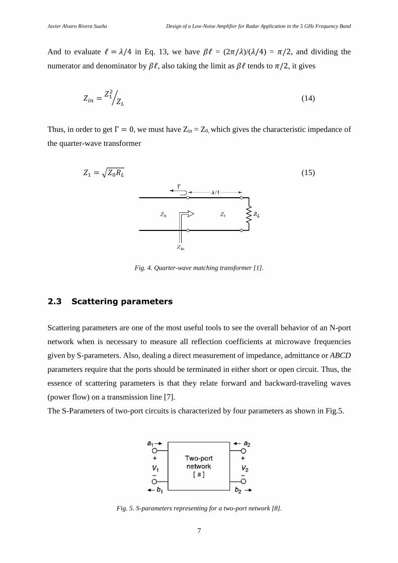
One of the most common intermediate circuit for impedance matching is the quarter-wave
transformer, which implies a transmission line. Thus, the input impedance of the right-hand
transmission line shown in Fig.4. is given by Eq. (13).
𝑍𝑖𝑛 = 𝑍1𝑅𝐿+𝑗𝑍1 tan 𝛽ℓ
𝑍1+𝑗𝑅𝐿 tan 𝛽ℓ (13)
Javier Alvaro Rivera Suaña Design of a Low-Noise Amplifier for Radar Application in the 5 GHz Frequency Band
7
And to evaluate ℓ = 𝜆/4 in Eq. 13, we have 𝛽ℓ = (2𝜋/𝜆)/(𝜆/4) = 𝜋/2, and dividing the
numerator and denominator by 𝛽ℓ, also taking the limit as 𝛽ℓ tends to 𝜋/2, it gives
𝑍𝑖𝑛 =𝑍1
2
𝑍𝐿⁄ (14)
Thus, in order to get Γ = 0, we must have Zin = Z0, which gives the characteristic impedance of
the quarter-wave transformer
𝑍1 = √𝑍0𝑅𝐿 (15)
Fig. 4. Quarter-wave matching transformer [1].
2.3 Scattering parameters
Scattering parameters are one of the most useful tools to see the overall behavior of an N-port
network when is necessary to measure all reflection coefficients at microwave frequencies
given by S-parameters. Also, dealing a direct measurement of impedance, admittance or ABCD
parameters require that the ports should be terminated in either short or open circuit. Thus, the
essence of scattering parameters is that they relate forward and backward-traveling waves
(power flow) on a transmission line [7].
The S-Parameters of two-port circuits is characterized by four parameters as shown in Fig.5.
Fig. 5. S-parameters representing for a two-port network [8].

Javier Alvaro Rivera Suaña Design of a Low-Noise Amplifier for Radar Application in the 5 GHz Frequency Band
8
From the figure above the S-parameters can be represented by the relationship between 𝑎𝑛
and 𝑏𝑛 as follow [8].
𝑎𝑛 =𝑣𝑛
+
√𝑍𝑂𝑛 ; Proportional to the incoming wave at the nth port
𝑏𝑛 =𝑣𝑛
−
√𝑍𝑂𝑛 ; Proportional to the outgoing wave at the nth port
Where 𝑣𝑛+ and 𝑣𝑛
− represent voltages corresponding to the incoming and the outgoing waves in
the transmission line connected to the nth port and 𝑍𝑂𝑛 (characteristic impedance) of the line;
thus, the relationship between 𝑎𝑛 and 𝑏𝑛 can be written as
𝑏1 = 𝑆11𝑎1 + 𝑆12𝑎2
𝑏2 = 𝑆21𝑎1 + 𝑆22𝑎2
Therefore, we have
𝑆11 =𝑏1
𝑎1, 𝑆21 =
𝑏2
𝑎1, 𝑎2 = 0
𝑆12 =𝑏1
𝑎2, 𝑆22 =
𝑏2
𝑎2, 𝑎1 = 0
Where
𝑆11= Input reflection coefficient
𝑆21= Forward transmission coefficient
𝑆12= Reverse transmission coefficient
𝑆22= Output reflection coefficient
2.4 Microwave transistor amplifier
2.4.1 Gain
Since voltage and current are extremely difficult to measure at high frequencies, it is much
easier to measure signal power. At the same time, the interstage impedance levels achievable
at high frequencies are neither very high nor very small, making power, rather than voltage gain
or current gain, critically important in high-frequency circuit design.

Javier Alvaro Rivera Suaña Design of a Low-Noise Amplifier for Radar Application in the 5 GHz Frequency Band
9
We will consider an arbitrary two-port network, characterized by its S-parameters connected to
the source and load impedance ZS and ZL, respectively, as shown in Fig. 6 to define the power
gains acting on the two-port network.
The power gain, G = PL/Pin is defined as the power dissipated in the load divided by the
power delivered to the input of the two-port network. It is independent of the signal
source impedance ZS.
The available power gain, GA = Pavn/Pavs is defined as the power available from the two-
port network divided by the power available from the signal source. It assumes
conjugate matching of the source and of the load, thus, it is dependent on the signal
source impedance, but not on the load impedance ZL.
Transducer power gain, GT = PL/Pavs is one the most useful figures for an amplifier,
which is the ratio of the power delivered to the load of the power delivered by the source
and it depends on the input and output match. Thus, in terms of the gain coefficients,
the transducer gain is GT = GSG0GL. And in terms of reflection coefficients, the
transducer gain is given as:
𝐺𝑇 =1 − |Γ𝑠|2
|1 − Γ𝑖𝑛Γ𝑠|2|𝑆21|2
1 − |Γ𝐿|2
|1 − 𝑆22Γ𝐿|2
Fig. 6. Transistor amplifier circuit [1].
2.4.2 Stability
The stability is a necessary condition for a transistor amplifier to guarantee the right
performance of an LNA design in a stable region. Thus, there are two types of stability:
|Γ𝑖𝑛| = |𝑆11 +𝑆12𝑆21Γ𝐿
1 − 𝑆22Γ𝐿| < 1
|Γ𝑜𝑢𝑡| = |𝑆22 +𝑆12𝑆21Γ𝑆
1 − 𝑆11Γ𝑆| < 1
Javier Alvaro Rivera Suaña Design of a Low-Noise Amplifier for Radar Application in the 5 GHz Frequency Band
10
Unconditional stability, where the input and output reflection coefficients are
|Γ𝑖𝑛| < 1 𝑎𝑛𝑑 |Γ𝑜𝑢𝑡| < 1
For all passive source and load impedances.
Conditional stability, where the input and output reflection coefficient are
|Γ𝑖𝑛| < 1 𝑎𝑛𝑑 |Γ𝑜𝑢𝑡| < 1
Only for a certain range of passive source and load impedances.
Thus, the stability is needed before to make the design of an amplifier and can determine the
stability region for Γ𝑠 and Γ𝐿. To analyze this stability condition, it can be determined by using
the Rollet’s condition as defined below
𝐾 =1 − |𝑆11|2 − |𝑆22|2 + |Δ|2
2|𝑆12𝑆21|> 1
Where
|Δ| = |𝑆11𝑆22 − 𝑆12𝑆21| < 1
2.4.3 Maximum gain (conjugate matching)
To get the maximum gain between the Source and Load impedances of the transistor, it must
be realized when the Source and Load reflection coefficients provide a conjugate matching on
them. Thus, the maximum power transfer from the input matching network to the transistor will
occur when
Γ𝑖𝑛 = Γ𝑆∗
And the maximum power transfer from the transistor to the output matching network will occur
when
Γ𝑜𝑢𝑡 = Γ𝐿∗

Javier Alvaro Rivera Suaña Design of a Low-Noise Amplifier for Radar Application in the 5 GHz Frequency Band
11
With those assumptions for lossless matching networks, the overall transducer gain for
maximum gain will be given by
𝐺𝑇𝑚𝑎𝑥 = 1
1 − |Γ𝑆|2|𝑆21|2
1 − |Γ𝐿|2
|1 − 𝑆22Γ𝐿|2
And, the necessary equations to get the maximum gain in a bilateral case is as follow
Γ𝑆∗ = 𝑆11 +
𝑆12𝑆21Γ𝐿
1 − 𝑆22Γ𝐿
Γ𝐿∗ = 𝑆22 +
𝑆12𝑆21Γ𝑆
1 − 𝑆11Γ𝑆
Where the solution of Γ𝑆 and Γ𝐿 are given as
Γ𝑆 =𝐵1 ± √𝐵1
2 − 4|𝐶1|2
2𝐶1
Γ𝐿 =𝐵2 ± √𝐵2
2 − 4|𝐶2|2
2𝐶2
The variables B1, C1, B2, C2 are defined as
𝐵1 = 1 + |𝑆11|2 − |𝑆22|2 − |∆|2
𝐵2 = 1 + |𝑆22|2 − |𝑆11|2 − |∆|2
𝐶1 = 𝑆11 − ∆𝑆22∗
𝐶2 = 𝑆22 − ∆𝑆11∗
2.4.4 Low-noise
The noise figure of a two-port amplifier can be expressed as
𝐹 = 𝐹𝑚𝑖𝑛 +𝑅𝑁
𝐺𝑆|𝑌𝑠 − 𝑌𝑜𝑝𝑡|
2
Where
YS = Source admittance presented to transistor.
Yopt = Optimum source admittance to get minimum noise figure.

Javier Alvaro Rivera Suaña Design of a Low-Noise Amplifier for Radar Application in the 5 GHz Frequency Band
12
Fmin= Minimum noise figure of transistor
RN = Equivalent noise resistance of transistor.
GS= Real part of source admittance.
Thus, in order to achieve the minimum noise in a LNA design, it must be applied that
Ys = Yopt
2.4.5 Cascaded noise figure
Noise figure is one of the most important parameters, when we are designing a Low-noise
amplifier, especially in cascaded amplifiers, where the cumulative noise figure of two or more
cascaded amplifiers is described by Eq. (16), which is defined as Friis’s equation [9].
Fig. 7. shows the gain and noise figure of the individual stages of a cascade transistor amplifier.
Fig. 7. Cascade transistor amplifiers.
𝐹𝑡𝑜𝑡𝑎𝑙 = 𝐹1 +𝐹2−1
𝐺1+
𝐹3−1
𝐺1𝐺2+ ⋯
𝐹𝑛−1
𝐺1𝐺2𝐺3…𝐺𝑛 (16)
Where:
Ftotal = Noise figure of the amplifiers cascaded together
Fn = Noise figure of the nth amplifier
Gn = Gain of the nth amplifier
Thus, in a cascade amplifier, the final stage sees an input signal that consists of the original
signal and noise amplified by each successive stage. Each stage in the cascade chain amplifies
signal and noise from previous stages and contributes some noise of its own. As we can see in
Eq. (16). the noise figure of the entire cascade chain is dominated by the noise contribution of
the first stage or two; later stages are less important where noise is concerned, provided that the
input stages have sufficient gain.

Javier Alvaro Rivera Suaña Design of a Low-Noise Amplifier for Radar Application in the 5 GHz Frequency Band
13
2.4.6 Gain compression
Gain compression is a usual behavior of a typical microwave amplifier, especially, when we
are plotting the output power as a function of input power. At low power levels, a single
frequency signal is increased in power level by the small signal gain, as Pout = G *Pin, where at
lower power levels, this produces a linear Pout versus Pin plot with slope equals one.
At higher levels, nonlinearities in the amplifier begin to generate some power in the harmonics
of the single frequency input signal and to compress the output signal. Therefore, gain
compression is often characterized in terms of the power level when the large signal gain is 1
dB less than the small gain, as shown in Fig. 8.
Fig. 8. Gain compression behavior.

Javier Alvaro Rivera Suaña Design of a Low-Noise Amplifier for Radar Application in the 5 GHz Frequency Band
14
3 Design
3.1 Characterization of the substrate
3.1.1 Dielectric constant (𝝐𝒓)
The purpose of this characterization is to find the most accurate value of the dielectric constant
(𝜖𝑟) of the substrate used, which is correlated with the design frequency. The task will be
designing and manufacturing a resonator circuit at 2.5 GHz, to later on, make it an adjustment
with the schematic and momentum simulations, in order to do an average of those values of the
dielectric constant.
To carry out this resonator design, we will take the parameters of the substrate given by the
manufacturer.
𝜖𝑟 = 4.4 ; Dielectric constant
𝐻 = 0.4 𝑚𝑚 ; Thickness of the substrate
tan 𝛿 = 0.02 ; Loss tangent
𝑇 = 35 𝜇𝑚 ; Thickness of the conductor
As we can see in Fig. 9. The quarter-wave resonator has been designed at 2.5 GHz.
Fig. 9. Quarter-wave resonator circuit.
Once we have designed the resonator circuit, we proceed to measure it, where, we got different
frequencies from the schematic simulation at 2.499 GHz and momentum simulation at 2.477
GHz, while VNA measurement at 2.544 GHz. As shown in Fig. 10.

Javier Alvaro Rivera Suaña Design of a Low-Noise Amplifier for Radar Application in the 5 GHz Frequency Band
15
Fig. 10. Resonance frequencies obtained from the quarter-wave circuit.
Then, due to the different resonance frequencies obtained, the task was to do a tuning on the
dielectric parameter of the schematic and momentum design, in order to get the same frequency
as VNA measurement at 2.544 GHz. After doing that process, we got the dielectric constants;
from the schematic simulation at 4.23 and momentum simulation at 4.19, which are different
from each other. As shown in Fig. 11.
Thus, the dielectric constant taken to design the amplifiers was 𝜖𝑟 = 4.21, which was obtained
as an average of the schematic and momentum values.
Fig. 11. Dielectric constants (𝜖𝑟) obtained after made the tuning.
Javier Alvaro Rivera Suaña Design of a Low-Noise Amplifier for Radar Application in the 5 GHz Frequency Band
16
3.1.2 Loss tangent (𝐭𝐚𝐧 𝜹)
For this purpose, we will take as a reference the reflection coefficient S11 measured by VNA at
the resonance frequency obtained (2.544 GHz) to make a tuning on the schematic design circuit
from the Fig. 9.
As we can see in Fig. 12 (left side), it shows S11 (schematic simulation) compared to the VNA
measurement result, both responses with tan 𝛿 equals 0.02, but, we can see on it that the VNA
attenuation result is more than the schematic attenuation result. Thus, we did a tuning on tan 𝛿
from the schematic design, in order to achieve almost the same attenuation as the VNA result,
as we can see in Fig. 12 (right side), the tuning on tan 𝛿 parameter for the Schematic design is
giving 0.042.
Fig. 12. Characterization for the 𝑡𝑎𝑛 𝛿 of the substrate.

Javier Alvaro Rivera Suaña Design of a Low-Noise Amplifier for Radar Application in the 5 GHz Frequency Band
17
3.2 Selection of the transistor
Since our LNA design will work at 5 GHz, and in order to achieve the minimum noise at the
first stage of the amplifier and the maximum gain at the second stage of it; High Electron
Mobility Transistor HEMT (ATF-34143) by AVAGO Technology is ideal for this type of
requirements due to its excellent combination of low noise performance for a wider frequency
range, high gain and high output power [10].
Also as a recommendation from the manufacturer, we will design the recommended PCB Pad
Layout dimensions for this transistor given on data sheet, as shown in Fig. 13.
Fig. 13. Pin connections and recommended PCB pad Layout for the transistor.
3.2.1 DC-bias point for the transistor
In order to get the right performance of the transistor (ATF-34143), we will choose a proper
DC-bias point for it. And by checking the available Drain-Source Voltage (VDS) and Drain-
Source Current (IDS) for different scattering parameters given on data sheet, as follow
VDS = 3V, IDS = 20 mA
VDS = 3V, IDS = 40 mA
VDS = 4V, IDS = 40 mA
VDS = 4V, IDS = 60 mA
Where, it was necessary to apply the condition for unconditional stability on S-parameters for
VDS = 4V and IDS = 40 mA, the Rollet’s factor (K) was more than one at the design frequency
of 5 GHz. Thus, we chose VDS = 4V and IDS = 40 mA as DC- bias point for the transistor.

Javier Alvaro Rivera Suaña Design of a Low-Noise Amplifier for Radar Application in the 5 GHz Frequency Band
18
Fig. 14. shows the circuit for the transistor to find the proper DC-bias point of the voltage Gate-
Source (VGS).
Fig. 14. DC-bias circuit for the transistor ATF-34143.
After doing the simulation of the DC-bias circuit to get the proper Voltage Gate-Source (VGS)
of the transistor, we got -0.54 V as the proper value. As shown in Fig. 15.
Fig. 15. Simulated IDS – VDS from the ATF-34143 transistor.

Javier Alvaro Rivera Suaña Design of a Low-Noise Amplifier for Radar Application in the 5 GHz Frequency Band
19
3.3 Selection of the DC-blocking capacitor
In order to get a proper capacitor for DC blocking and coupling, it is necessary to consider
typical requirements like capacitance, tolerance and voltage rating at the design frequency.
Thus, there is a suitable capacitor model TDK (multilayer ceramic chip capacitor) to covers all
these requirements. The 100 nF capacitor will be used in this project, with
(TDK_C1608X8R1E104K080AA) taken as a reference model.
3.4 DC-bias circuit for the transistor
To perform the DC-bias circuit for the transistor amplifier, it is convenient to use a quarter-
wave transmission line at the fundamental frequency to be able to do the connection between
the Drain of the transistor and the DC-supply, similarly for the Gate of the transistor. This
quarter-wave has the advantage of being as an open circuit at the fundamental frequency [11].
This advantage is important in order to avoid that the RF-signal goes to the DC-supply, also to
strengthen this design at the end of the quarter-wave, we will be placed a radial resonator stub
to guarantee a short-circuit.
As we can see in Fig. 16. An example of a circuit to place the quarter-wave transformer as a
part of the DC-bias network for the transistor.
Fig. 16. Quarter-wave short circuit stub [11].

Javier Alvaro Rivera Suaña Design of a Low-Noise Amplifier for Radar Application in the 5 GHz Frequency Band
20
3.4.1 Design of microstrip radial resonator
Since this radial resonator needs to generate an RF-short circuit at the end of the quarter-wave
transformer. Thus, it will be designed to work at 5 GHz and to achieve this requirement, this
radial will depend on three dimensions like its width, length, and angle. As shown in Fig. 17.
Fig. 17. The design circuit for the radial resonator.
As we can see in Fig. 18 the impedance obtained from the simulation of the radial circuit is -
68.558 dB.
Fig. 18. Impedance response from the radial resonator.

Javier Alvaro Rivera Suaña Design of a Low-Noise Amplifier for Radar Application in the 5 GHz Frequency Band
21
3.4.2 Design of microstrip RF choke
Working at high frequencies, it is necessary to use an RF-choke circuit that is used to suppress
the AC signals while passing the DC signal. Ideally, it is an inductor with infinite inductance
value and low resistance [12].
To perform this RF-choke circuit for biasing the transistor, it is suitable to add a small
transmission line (MTaper) to link the Gate and Drain paths of the transistor, in order to have
more flexibility at the time when we will make the manufacture of the amplifier, and also to
consider into RF-choke circuit. Therefore, to be able to connect the Gate and Drain paths of
the transistor to the DC-supply, this RF choke is used for this purpose by using quarter-wave
transformer between those terminals of the transistor and the DC supply. The quarter-wave
transformer is designed to work at high impedance with 0.4 mm of width to achieve an open
circuit while the RF-signal will go throughout the RF-signal path; then at the end of this quarter-
wave transmission line will be placed the radial resonator. Also, we added two transmission
lines to be able to connect the DC-supply for the transistor, as shown in Fig. 19.
Fig. 19. RF-choke circuit.
Fig. 20 shows the results of this RF-choke circuit, where the forward transmission coefficient
(S21) is getting an attenuation of -0.132 dB for the RF-signal path, while the transmission (S31)

Javier Alvaro Rivera Suaña Design of a Low-Noise Amplifier for Radar Application in the 5 GHz Frequency Band
22
gets an attenuation of -99.796 dB, which means if the RF-signal could reach this point, it will
act as a virtual ground or short-circuited.
Fig. 20. Results from the RF-Choke circuit.
3.5 Maximum-gain amplifier
3.5.1 Schematic design
Since we have the RF-choke circuit for the transistor. We will design the maximum-gain
amplifier by using the DC-bias network shown in Fig. 21. Also, we will use the S2P file to
simulate the transistor. But, we must first check the stability of the DC-bias network.
Fig. 21. DC-bias network for the maximum-gain amplifier.

Javier Alvaro Rivera Suaña Design of a Low-Noise Amplifier for Radar Application in the 5 GHz Frequency Band
23
After doing the simulation of the DC-bias network, we obtained the stability factor, which is
given by Rollet’s condition (k) that is more than one (1.063), meaning also that the DC-bias
network is unconditionally stable to guarantee that both input and output reflection coefficients
must be less than one (|Γ𝑖𝑛| < 1, |Γ𝑜𝑢𝑡| < 1) as well.
And, as we can see in Fig. 22. The source and load stability circles are outside of the Smith
chart, where we can assume that inside of the Smith chart is unconditionally stable region by
applying the requirements below
|Γ𝑖𝑛| = |𝑆11 +𝑆12𝑆21Γ𝐿
1 − 𝑆22Γ𝐿| < 1
|Γ𝑜𝑢𝑡| = |𝑆22 +𝑆12𝑆21Γ𝑆
1 − 𝑆11Γ𝑆| < 1
Thus, we must satisfy that Γ𝐿 and Γ𝑆 should be zero, regarding having |Γ𝑖𝑛|=S11 and |Γ𝑜𝑢𝑡|=S22
into above requirements. Therefore, we just need to analyze the absolute value of S11 and S22,
where both reflection coefficients are giving less than one, which are satisfying the above
requirements, also, they are representing that the whole region inside of the Smith chart is
unconditionally stable.
Fig. 22. Source and load stability circles.
S-parameters obtained from the simulation of the DC-bias network are given as follow

Javier Alvaro Rivera Suaña Design of a Low-Noise Amplifier for Radar Application in the 5 GHz Frequency Band
24
Since the stability of the DC-bias network has been analyzed and the stable regions for Source
and Load have been located on the Smith chart,
We need to find the necessary reflection coefficients at the input and output of the DC-bias
network to get the maximum gain achievable by the transistor, where we must apply the
conjugate matching on the DC-bias network by applying the necessary equations given in
Subsection 2.4.3, where Γ𝑖𝑛 = Γ𝑠∗ and Γ𝑜𝑢𝑡 = Γ𝐿
∗, as shown in Fig. 23.
Fig. 23. Conjugate reflection coefficients.
Then, we can do the matching networks for the input and output of the DC-bias network by
taking up the conjugate reflection coefficients given by Γ𝐿 and Γ𝑆, and place them in the center
of the Smith chart. ADS provide us an essential tool for this purpose that is SmithChart, where
at the same time it can generate ideal transmission lines with effective dielectric constants (휀𝑒)
at the characteristic impedance (50 Ω). And, to be able to have these matching networks in
microstrip lines, they must be converted as length (mm) and width (mm) by using Linecal tools.
Then, to be able to connect the SMA terminals to the ports for the amplifier, we must add
characteristic transmission lines for the input and output. Also, it is better to add the MTEE
junction between the matching networks and the characteristic transmission lines for the ports.
After placing all these components on the design amplifier, it is convenient to do an adjustment
onto lengths of the matching networks to make sure that both conjugate coefficients Γ𝐿 and Γ𝑆
are placed in the center of the Smith chart.
Javier Alvaro Rivera Suaña Design of a Low-Noise Amplifier for Radar Application in the 5 GHz Frequency Band
25
Thus, placing both conjugate coefficients in the center of the Smith chart, the overall transducer
power gain of the amplifier will be controlled by the Source and Load gains of the matching
networks.
Fig. 24 shows the full design for the amplifier to get the maximum gain by the transistor.
Fig. 24. Maximum-gain amplifier.

Javier Alvaro Rivera Suaña Design of a Low-Noise Amplifier for Radar Application in the 5 GHz Frequency Band
26
Since we have fixed the conjugate matching networks for the amplifier, and after doing the
simulation of it. We can notice that both conjugate coefficients Γ𝐿 and Γ𝑆 are placed in the center
of the Smith chart. As shown in Fig. 25.
Fig. 25. Conjugate reflections 𝛤𝐿 𝑎𝑛𝑑 𝛤𝑆 matched.
Fig. 26 shows the S-parameters from the simulation of the maximum-gain amplifier. Thus, the
maximum gain provided by the amplifier is 10.409 dB, where the forward coefficient S21
reaches that maximum gain due to the conjugate matching. Also, we can see that both reflection
coefficients S11 and S22 are matching the amplifier at the fundamental frequency.
Fig. 26. S-Parameters from the maximum-gain amplifier.

Javier Alvaro Rivera Suaña Design of a Low-Noise Amplifier for Radar Application in the 5 GHz Frequency Band
27
3.5.2 EM-cosimulation design
Since we have completed with the schematic design and simulation of the maximum-gain
amplifier, it was also suitable to do the EM-Cosimulation for the amplifier, in order to have
more accurate results as compared to the schematic results. Since the amplifier is generated in
a real layout to be able to simulate it. Thus, all components were placed again on this layout.
As shown in Fig. 27.
Fig. 27. Layout generated for the maximum-gain amplifier.
Fig. 28. shows the results obtained from EM-cosimulation of the layout generated for the
maximum-gain amplifier, where the maximum gain achieved is 10 dB by the forward
coefficient S21, while S11 is -17.063 dB and S22 is -22.148 dB
Fig. 28. EM-cosimulation results from the maximum-gain amplifier.

Javier Alvaro Rivera Suaña Design of a Low-Noise Amplifier for Radar Application in the 5 GHz Frequency Band
28
3.6 Minimum-noise amplifier
3.6.1 Schematic design
For this design, we will choose the same transistor due to it is ideal for minimum noise and high
linearity behavior. Since we have changed the tan 𝛿 parameter, the DC-bias network for the
minimum-noise amplifier will be a little different from the DC-bias network for the maximum-
gain amplifier, regarding the dimensions of the radial resonator and the quarter-wave
transformer. Thus, in this design, we will consider the new tan 𝛿 (0.042) parameter to design
the whole minimum-noise amplifier. Therefore, the parameters characterized for the substrate
will be as follow
𝜖𝑟 = 4.21 ; Dielectric constant
tan 𝛿 = 0.042 ; Loss tangent
As we can see in Fig. 29. the DC-bias network for the minimum-noise amplifier has been
designed.
Fig. 29. DC bias network for the minimum-noise amplifier.
After doing the simulation of the DC-bias network for the minimum-noise amplifier, the
stability factor given by Rollet’s condition (k) is unconditionally stable due to k = 1.051. Then,
we can do the matching networks for the transistor. Thus, in order to achieve the minimum

Javier Alvaro Rivera Suaña Design of a Low-Noise Amplifier for Radar Application in the 5 GHz Frequency Band
29
noise at the input of the transistor, we must set up 𝛤𝑆 = 𝛤𝑜𝑝𝑡, as we discussed in subsection
2.4.4, where ADS provide this optimum reflection coefficient as Sopt
And to be able to get the maximum gain achievable at the output of the transistor, it is necessary
to satisfy 𝛤𝑜𝑢𝑡 = 𝛤𝐿∗, which is given by
Γ𝑜𝑢𝑡 = (𝑆22 +𝑆12𝑆21𝑆𝑜𝑝𝑡
1 − 𝑆11𝑆𝑜𝑝𝑡)
∗
As we can see in Fig. 30. both reflection coefficients Sopt and 𝛤𝐿∗ have been measured.
Fig. 30. Optimum and conjugate coefficients for the minimum-noise amplifier.
Since we have both reflection coefficient Sopt and 𝛤𝐿∗, we will match the amplifier by using the
Smith Chart tool of ADS, since they will be in ideal transmission lines, we will convert them
into microstrip lines by using LineCal tool.
where it will be also necessary to add two characteristic transmission lines (50 Ω) at the input
and output for the minimum-noise amplifier, in order to make the connection of SMA terminal.
Then, an adjustment will be needed in the whole amplifier in order to avoid mismatch of the
matching networks.

Javier Alvaro Rivera Suaña Design of a Low-Noise Amplifier for Radar Application in the 5 GHz Frequency Band
30
As we can see in Fig. 31. The matching networks for the minimum-noise amplifier have been
designed.
Fig. 31. Minimum-noise amplifier.

Javier Alvaro Rivera Suaña Design of a Low-Noise Amplifier for Radar Application in the 5 GHz Frequency Band
31
After the matching networks were fixed for the minimum-noise amplifier, we can notice that
𝑆𝑜𝑝𝑡 and 𝛤𝐿∗ are placed in the center of the Smith chart, see Fig. 32.
Fig. 32. Reflection coefficients matched for the minimum-noise amplifier.
Fig. 33. shows the results from the simulation of the minimum-noise amplifier, where the
forward coefficient S21 is 7.769 dB, while, both reflection coefficients 𝑆𝑜𝑝𝑡 and 𝛤𝐿∗ are well
matched to get the minimum noise at the input and maximum gain at the output of the amplifier.
Also, we can see that the input reflection coefficient S11 is not matched at all; this behavior of
S11 is usual since we are matching the optimum coefficient 𝑆𝑜𝑝𝑡 at the input of the transistor
instead of S11.
Fig. 33. S-parameters results from the minimum-noise amplifier.

Javier Alvaro Rivera Suaña Design of a Low-Noise Amplifier for Radar Application in the 5 GHz Frequency Band
32
Since this minimum-noise amplifier will be placed at the first stage of the cascaded amplifier,
thus, the entire noise figure (NF) of the cascaded amplifier will be dominated by the first stage
as we discussed in Subsection 2.4.5
As we can see in Fig. 34. The simulation of the minimum-noise amplifier is getting a noise
figure of 1.217 dB since the matching network has been performed to get the minimum noise
at the input of the amplifier, also the specific noise figure “nf(2)” provided by ADS is reaching
this minimum noise.
Fig. 34. Noise figure achieved from the amplifier.
3.6.2 EM-cosimulation design
To be able to have more accurate results from the minimum-noise amplifier, we performed the
EM-cosimulation of it, in order to consider the schematic and electromagnetic simulations.
Fig. 35 shows the layout for the minimum-noise amplifier.
Fig. 35. Layout for the minimum-noise amplifier.
Javier Alvaro Rivera Suaña Design of a Low-Noise Amplifier for Radar Application in the 5 GHz Frequency Band
33
As we can see in Fig. 36. the EM-cosimulation results from the minimum-noise amplifier,
where the optimum coefficient 𝑆𝑜𝑝𝑡 is -18.561 dB of attenuation, while S22 is -15.303 dB, thus,
with these values, we are satisfying the necessary requirements to get the minimum noise from
the amplifier.
Nevertheless, we got 7.942 dB gain, which is quite lower as compared to the maximum-gain
amplifier.
Fig. 36. EM-cosimulation results from the minimum-noise amplifier.

Javier Alvaro Rivera Suaña Design of a Low-Noise Amplifier for Radar Application in the 5 GHz Frequency Band
34
3.7 Design of two-stage LNA
To carry out this part of the project, it will be designed just as a software design, since the
substrate used to make the manufacture of the amplifiers has a tan 𝛿 more than a usual substrate.
3.7.1 First stage
Since we have designed each amplifier separately, in this step we will design a cascaded LNA
in a single circuit. For this purpose, we will take the DC-bias networks from the previous design,
in order to obtain the coefficients of 𝑆𝑜𝑝𝑡 and Γ𝐿∗ for this first stage (minimum noise). As we
have discussed before this configuration of the DC-bias is unconditionally stable.
Therefore, after doing the simulation of this DC-bias network, we can obtain the necessary
coefficients to do the matching networks, which are given as follow
𝑆𝑜𝑝𝑡 = 0.437 − 𝑗0.485
Γ𝐿∗ = 0.853 − 𝑗0.896
3.7.2 Second stage
To be able to have the second stage of the cascaded amplifier working in maximum gain, it is
necessary to apply the conjugate matching coefficients discussed in subsection 2.4.3, regarding
having Γ𝑖𝑛 = Γ𝑠∗ and Γ𝑜𝑢𝑡 = Γ𝐿
∗, since the DC-bias network is unconditionally stable as well,
we can obtain these conjugate coefficients by fixing the conjugate equations in ADS, which are
given as follow
Γ𝑠∗ = 0.285 − 𝑗1.369
Γ𝐿∗ = 0.331 − 𝑗0.557
3.7.3 Intermediate matching network
Since we have both DC-bias networks for the minimum noise and maximum-gain amplifier. In
order to do the matching network between those amplifiers. We will take the output conjugate
coefficient from the minimum-noise amplifier that is 0.853-j0.896 and the input conjugate
coefficient from the maximum-gain amplifier, which is 0.285-j1.369, thus, we can do the
matching network for those coefficients by using the Smith chart tools of ADS. And making
Javier Alvaro Rivera Suaña Design of a Low-Noise Amplifier for Radar Application in the 5 GHz Frequency Band
35
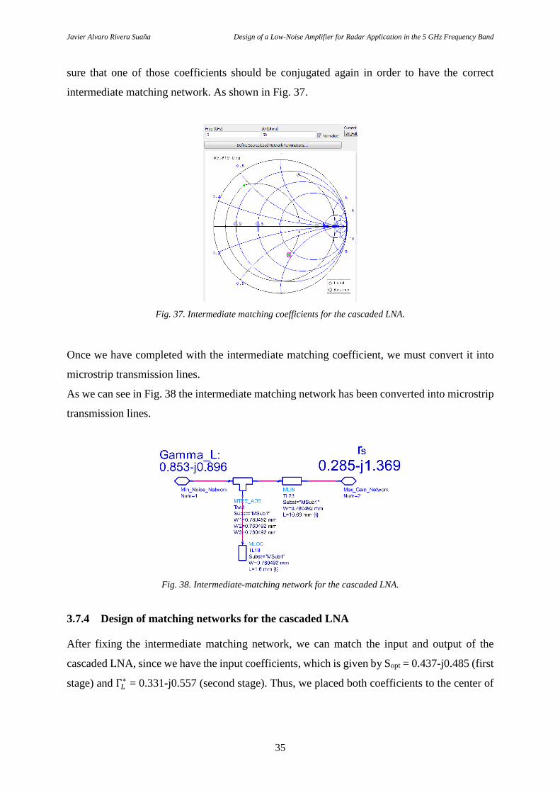
sure that one of those coefficients should be conjugated again in order to have the correct
intermediate matching network. As shown in Fig. 37.
Fig. 37. Intermediate matching coefficients for the cascaded LNA.
Once we have completed with the intermediate matching coefficient, we must convert it into
microstrip transmission lines.
As we can see in Fig. 38 the intermediate matching network has been converted into microstrip
transmission lines.
Fig. 38. Intermediate-matching network for the cascaded LNA.
3.7.4 Design of matching networks for the cascaded LNA
After fixing the intermediate matching network, we can match the input and output of the
cascaded LNA, since we have the input coefficients, which is given by Sopt = 0.437-j0.485 (first
stage) and Γ𝐿∗ = 0.331-j0.557 (second stage). Thus, we placed both coefficients to the center of

Javier Alvaro Rivera Suaña Design of a Low-Noise Amplifier for Radar Application in the 5 GHz Frequency Band
36
the Smith chart. Where it was also necessary to do an adjustment in the whole amplifier since
we added two characteristic transmission lines for the SMA terminals.
As we can see in Fig. 39 all matching networks have been designed.
Fig. 39. Cascaded LNA.
Therefore, we can see in Fig. 40 that the matching networks are placing the coefficients 𝑆𝑜𝑢𝑡
and Γ𝐿∗ to the center of the Smith chart.
Fig. 40. Input and output coefficients matched.

Javier Alvaro Rivera Suaña Design of a Low-Noise Amplifier for Radar Application in the 5 GHz Frequency Band
37
Fig. 41 shows the results from the simulation of the cascaded LNA, where S21 is 14.961 dB of
gain, also the optimum coefficient is -71 dB of attenuation and the output reflection coefficient
S22 is -70 dB as well.
Fig. 41. Schematic results from the cascaded LNA.
Since the first stage from the cascaded LNA is designed to get the minimum noise, we can see
that the overall noise figure is covered by the first stage, which is 1.293 dB of noise figure. As
shown in Fig. 42.
Fig. 42. Minimum-noise achieved from the cascaded LNA.

Javier Alvaro Rivera Suaña Design of a Low-Noise Amplifier for Radar Application in the 5 GHz Frequency Band
38
3.7.5 EM-cosimulation for the cascaded LNA.
In order to have more accurate results from the cascaded LNA, we performed the EM-
cosimulation of it.
Fig. 43 shows the layout for the cascaded LNA.
Fig. 43. Layout generated for the cascaded LNA.
Fig. 44 shows the results from the EM-cosimulation for the cascaded LNA.
Fig. 44. EM-cosimulation results from the cascaded LNA.

Javier Alvaro Rivera Suaña Design of a Low-Noise Amplifier for Radar Application in the 5 GHz Frequency Band
39
4 Manufacturing
Since we have the layout of the amplifiers and the resonator design (characterization of the
substrate), we performed the manufacture of them by using the insulator technique, following
the below steps.
4.1 Insulator technique
To be able to make the amplifiers, it was necessary to export them to the Gerber format
in ADS. In order to print them on a transparency film for laser printers. As shown in
Fig. 45.
Fig. 45. Transparency film printed with the amplifier design.
Since we have the transparency film of the amplifiers, they were exposed inside the
insulator with the substrate for 160 seconds.
Then a Positive-Type Board Developer concentration was used in order to check the
design of the amplifier in the substrate.
Finally, all components were placed on top of the substrate characterized with the
soldering tin. Then the substrate was placed inside the programmable desktop reflow
oven for 15 minutes to achieve 210 oC of temperature. As shown in Fig. 46.
Fig. 46. Programmable desktop reflow oven.

Javier Alvaro Rivera Suaña Design of a Low-Noise Amplifier for Radar Application in the 5 GHz Frequency Band
40
5 Measurements
5.1 Measurements equipment
5.1.1 E8363B network analyzer
To perform the measurements of the circuits designed, we used the E8363B Vector Network
Analyzer (VNA) in order to compare these results with the EM-cosimulation results. The
measured results have saved as S2P file to be able to represent them in ADS.
Fig. 47. Vector Network Analyzer E8363B.
5.1.2 N4693A electronic calibration module
The calibration of the VNA was done by using the N4693A electronic calibration module (see
Fig. 48), in order to measure the amplifiers over the desired range of frequency (2 GHz to 12
GHz). This operation was done with a simple one-connection operation to the module, which
offers excellent accuracy without spending the time to calibrate the VNA.
Fig. 48. Electronic calibration module N4693A.

Javier Alvaro Rivera Suaña Design of a Low-Noise Amplifier for Radar Application in the 5 GHz Frequency Band
41
5.2 Maximum-gain amplifier
Fig. 49. shows the comparison between the EM-cosimulation results and VNA measurements,
where the forward coefficient S21 measured is 7.629 dB. Nevertheless, the reflection
coefficients S11 measured is -22.888 dB, which is even better than the EM-cosimulation result,
also S22 measured is -17.021 dB. Thus, with these results obtained to get the maximum gain of
the amplifier, we can see that doing the EM-cosimulation, we will get more accurate results
that is going to look like VNA measurement.
Fig. 49. Comparison between the EM-cosimulation results and VNA measurements.
5.3 Minimum-noise amplifier
Fig. 50. shows the comparison between the EM-cosimulation and VNA results, as we can see
on it, the forward transmission coefficients S21 from the VNA measurement is 6.589 dB, which
is lower than the EM-cosimulation result that was 7.942 dB, while the input reflection

Javier Alvaro Rivera Suaña Design of a Low-Noise Amplifier for Radar Application in the 5 GHz Frequency Band
42
coefficient (S11) measured is -3.745 dB; since we designed this amplifier to get the minimum
noise achievable by the amplifier, this input coefficient (S11) will not be matched at all.
On the other side, the output reflection coefficient (S22) measured is -13.163 dB that is matched
well the amplifier, since we did the matching networks to get the maximum gain at the output
of the amplifier.
Therefore, the comparison between the EM-cosimulation and VNA measurement have been
done.
Fig. 50. Comparison between the EM-cosimulation results and VNA measurements.
5.4 Minimum noise and maximum-gain amplifier
To be able to do the measurement of the two amplifiers designed, it was necessary to use an
attenuator of 3 dB, since we have noticed from the schematic simulation results that at lower
frequencies from the fundamental frequency (5 GHz), the input reflection coefficient (S11) was
reflecting the RF-signal, this phenomenon is given by the transistor; since the stability condition

Javier Alvaro Rivera Suaña Design of a Low-Noise Amplifier for Radar Application in the 5 GHz Frequency Band
43
is frequency dependent, thus, at lower frequencies our DC-bias networks are not
unconditionally stable.
Fig. 51. shows the measurements from the minimum noise and maximum-gain amplifiers,
setting up in cascaded, where the forward transmission coefficient (S21) measured is 9.425 dB,
but taken into consideration the attenuator value of 3 dB, thus, we are getting 12.425 dB of
gain.
Since the first amplifier was designed to get the minimum noise, the input reflection coefficient
(S11) of the cascaded amplifier is -3.581 dB, also, as we discussed in subsection 2.4.4 the first
stage amplifier will dominate the noise figure for the two amplifiers, regarding Friis’s equation.
And, the output reflection coefficient (S22) from the cascaded amplifier is -17.247 dB which is
matching well the amplifier, since we did the conjugate matching at the output for the
maximum-gain amplifier.
Then, in order to get the minimum noise figure achieved from the cascaded amplifiers, we did
the EM-cosimulation, where it was 1.35 dB of noise figure.
Fig. 51. VNA measurement of the two-stage amplifier.
Javier Alvaro Rivera Suaña Design of a Low-Noise Amplifier for Radar Application in the 5 GHz Frequency Band
44
6 Discussion
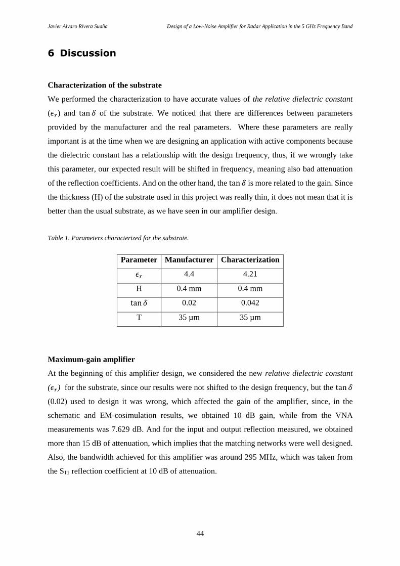
Characterization of the substrate
We performed the characterization to have accurate values of the relative dielectric constant
(𝜖𝑟) and tan 𝛿 of the substrate. We noticed that there are differences between parameters
provided by the manufacturer and the real parameters. Where these parameters are really
important is at the time when we are designing an application with active components because
the dielectric constant has a relationship with the design frequency, thus, if we wrongly take
this parameter, our expected result will be shifted in frequency, meaning also bad attenuation
of the reflection coefficients. And on the other hand, the tan 𝛿 is more related to the gain. Since
the thickness (H) of the substrate used in this project was really thin, it does not mean that it is
better than the usual substrate, as we have seen in our amplifier design.
Table 1. Parameters characterized for the substrate.
Parameter Manufacturer Characterization
𝜖𝑟 4.4 4.21
H 0.4 mm 0.4 mm
tan 𝛿 0.02 0.042
T 35 µm 35 µm
Maximum-gain amplifier
At the beginning of this amplifier design, we considered the new relative dielectric constant
(𝜖𝑟) for the substrate, since our results were not shifted to the design frequency, but the tan 𝛿
(0.02) used to design it was wrong, which affected the gain of the amplifier, since, in the
schematic and EM-cosimulation results, we obtained 10 dB gain, while from the VNA
measurements was 7.629 dB. And for the input and output reflection measured, we obtained
more than 15 dB of attenuation, which implies that the matching networks were well designed.
Also, the bandwidth achieved for this amplifier was around 295 MHz, which was taken from
the S11 reflection coefficient at 10 dB of attenuation.

Javier Alvaro Rivera Suaña Design of a Low-Noise Amplifier for Radar Application in the 5 GHz Frequency Band
45
Table 2. S-parameters obtained from the maximum-gain amplifier.
S-parameters Schematic (dB) Cosimulation (dB) VNA (dB)
S21 10.409 10.009 7.629
S12 -17.544 -17.512 -16.824
S11 -71.895 -17.063 -22.888
S22 -72.105 -22.148 -17.021
Minimum-noise amplifier
To design this minimum-noise amplifier, we used the tan 𝛿 (0.042) characterized, where the
gain measured was 6.589 dB also the coefficient S11 measured was -3.745 dB, which seems like
is not matching well the amplifier, because instead to use this coefficient S11, the optimum
coefficient Sopt was taken into account in order to have the minimum noise figure at the input
of this amplifier.
Thus, the minimum noise figure achieved from the simulation of this amplifier was 1.217 dB,
which is a little bit more than the expected results, which was less than 1 dB, it is clear the
substrate used to make the amplifier is affecting the expected results, nevertheless we will
measure both amplifiers characterized in order to get the gain and noise figure of the cascaded
LNA.
Table 3. S-parameters obtained from the minimum-noise amplifier.
S-parameters Schematic (dB) Cosimulation (dB) VNA (dB)
S21 7.769 7.942 6.589
S12 -20.184 -19.788 -18.370
Sopt -69.367 -18.559
S22 -74.241 -15.303 -13.163
S11 -5.068 -5.200 -3.745
Measurement of both amplifiers designed
Before to do the measurements of the amplifiers, it must be stated that at lower frequencies both
amplifier have unwanted signals (reflections) on input reflection coefficient S11, which is
clearly seen in Fig. 26 and Fig. 33, this behavior was due to the stability condition which is

Javier Alvaro Rivera Suaña Design of a Low-Noise Amplifier for Radar Application in the 5 GHz Frequency Band
46
frequency dependent, thus, the testing for unconditional stability given by Rollet’s condition
(K) at those frequencies are less than one, therefore, the amplifiers are unstable at those lower
frequencies.
Since we got unwanted signals at frequencies lower than the fundamental frequency (simulation
results), we used an attenuator of 3 dB, to be able to measure both amplifiers, where the gain
obtained considering also the attenuator value was 12.425 dB, also it is clear that the first stage
is dominating the whole system, because S11 remains as the previous measurement of the single
minimum-noise amplifier, where the minimum noise figure achieved was 1.35 dB, which was
getting from the EM-cosimulation of the two-stage amplifier designed.
Table 4. S-parameters obtained from the two stage amplifiers.
S-parameters VNA (dB)
S21 9.425
S12 -39.897
S11 -3.581
S22 -17.247
Design of a Cascaded LNA
Cascaded LNA was performed in order to compare with the amplifiers manufactured (minimum
noise and maximum gain), but this cascaded LNA was done just as in the software design and
as a single design. As we notice in Table 5. The gain obtained for this cascaded LNA is reaching
16.366 dB, while S11 remains at -3.836 dB, where Sopt is well matched to get the minimum noise
at the input of the amplifier, also the output coefficient S22 is well matched.
Table 5. EM-cosimulation results from the cascaded amplifier
S-parameters Schematic (dB) EM-Cosimulation (dB)
S21 14.961 16.366
S12 -40.945 -39.426
Sopt -71.034 -19.544
S22 -70.757 -11.870
S11 -2.897 -3.836

Javier Alvaro Rivera Suaña Design of a Low-Noise Amplifier for Radar Application in the 5 GHz Frequency Band
47
Gain compression.
To carry out this measurement to find the 1 dB gain compression from the amplifier
manufactured (maximum gain). We used the VNA to generate a sweep of power in it, thus, this
power was introduced to the input of the amplifier. Where we got for input power at 8.5 dBm
the gain of the amplifier, which was 7.629 dB gain, it reduced in 1 dB gain, therefore the gain
compression occurred at 8.5 dBm of input power, thus, the output power from the amplifier
will be at 16.229 dBm.

Javier Alvaro Rivera Suaña Design of a Low-Noise Amplifier for Radar Application in the 5 GHz Frequency Band
48
7 Conclusions
Minimum noise and maximum gain amplifiers have been designed and manufactured by using
the ATF-34143 transistor in an unconditionally stable region at 5 GHz. Setting up in a cascaded
the minimum noise and maximum-gain amplifier provided a noise figure of 1.35 dB and 12.425
dB gain at the fundamental frequency.
With these results, we could not cover the goal fixed at the beginning of this project due to the
gain is less than the expected result (more than 20 dB) and the minimum noise figure achieved
was 1.35 dB, which is more than the expected result (less than 1dB). Nevertheless, the gain and
noise figure characterized are acceptable, since more commercial LNA for radar applications
have more than 20 dB gain with a noise figure around 1.3 dB to 1.7 dB. Also, we have to
consider that to develop this project, we used cheaper components like the transistor and the
substrate, which also influenced with the results obtained.
In a future work, in these kinds of applications could be done better by using suitable
components, of which one of them should be the substrate, nowadays, there is available the
Rogers substrate (RO4003) with a tan 𝛿 parameter of 0.001 given by the manufacturer. Also,
to avoid unwanted signals close to the fundamental design frequency, it is convenient to place
a band pass filter in order to have just the desired range of frequency.

Javier Alvaro Rivera Suaña Design of a Low-Noise Amplifier for Radar Application in the 5 GHz Frequency Band
49
References
[1] D. M. Pozar, “Microwave Engineering”, 4th ed., John Willey & Sons, Inc., 2012, p. 1.
[2] R. E. Collin, “Foundations for Microwave Engineering”, 2nd ed., John Willey & Sons,
Inc., 2001, p. 3.
[3] P. Tait, “Introduction to Radar Target Recognition”, the Institution of Engineering and
Technology, IET Radar Series no 18, 2005, p. 55.
[4] M. Golio, J. Golio, “RF and Microwave Applications and Systems”, 2nd ed., Taylor &
Francis Group, LLC, 2008, p. 17.
[5] D. Fisher, I. J. Bahl, “Gallium Arsenide IC Applications Handbook”, vol. 1, Academic
Press, Inc., 1995, pp. 80-83.
[6] A. F. Peterson, G. D. Durgin, “Transient Signals on Transmission Lines: An Introduction
to Non-Ideal Effects and Signal Integrity Issues in Electrical Systems”, Morgan &
Claypool, 2009, pp. 3-7.
[7] M. Steer, “Microwave and RF Design a Systems Approach”, SciTech Publishing,
Raleigh, NC., 2010, pp. 299-300.
[8] I. J. Bahl, “Fundamentals of RF and Microwave Transistor Amplifiers”, John Wiley &
Sons, Inc., 2009, pp. 23-24.
[9] B. Henderson, E. Camargo, “Microwave Mixer Technology and Applications”, Artech
House, 2013, pp. 81-82.
[10] V. J. Kuhn, AlGaN/GaN-HEMT Power Amplifier with Optimized Power-Added
Efficiency for X-Band Applications, KIT Scientific Publishing, 2010, pp. 9-10
[11] S. C. Cripps, “RF Power Amplifiers for Wireless Communications”, 2nd ed., Artech
House, 2006, p. 104.
[12] M. Božanić, S. Sinha, “Power Amplifiers for S-, C-, X- and Ku-Bands: an EDA
Perspective”, Springer International Publishing Switzerland, 2016, p. 162.

Javier Alvaro Rivera Suaña Design of a Low-Noise Amplifier for Radar Application in the 5 GHz Frequency Band
A1
Appendix A
Measurement of S-parameters for the maximum-gain amplifier.
As we can see in Fig. A1. The maximum-gain amplifier was measured by using the VNA with
a suitable DC supply for the transistor (ATF-34143). And to carried out this process, it was
necessary to calibrate the VNA in order to have the desired range of frequency. The power DC
supply (3631A) was used to bias the transistor with an accurate DC supply.
Fig. A1. Measurements of the maximum-gain amplifier.
Fig. A2. Shows the S-parameters obtained from the maximum-gain amplifier.
Fig. A2. S-parameters from the maximum-gain amplifier.
Fig. A3 shows the amplifiers manufactured and the resonator circuit to characterize the
substrate.
Fig. A3. Circuits characterized.