Embed Size (px)
Citation preview
Journal of Engineering Science and Technology Vol. 12, No. 8 (2017) 2010 - 2027 © School of Engineering, Taylor’s University
2010
DESIGN OF A LOW-POWER AND HIGH THROUGHPUT ERROR DETECTION AND CORRECTION
CIRCUIT USING THE 4T EX-OR METHOD
S. KAVITHA*, FAZIDA HANIM HASHIM, MD MAMUN IBNE REAZ, NOORFAZILA KAMAL
Department of Electrical, Electronic and Systems Engineering, Universiti Kebangsaan
Malaysia, 43600, UKM, Bangi, Selangor, Malaysia
*Corresponding Author: [email protected]
Abstract
This paper describes an efficient implementation of an error correction circuit
based on single error detection and correction with check bit pre-computation.
The core component of the proposed 4-bit EX-OR circuit was designed using
the CMOS cascade method. This paper presents a 4-input EX-OR gate that was
developed from a 2-input EX-OR gate using the bit slice method. The proposed
architecture retains the modified Error Correction Code (ECC) circuit. The
proposed 4-input EX-OR gate and its auxiliary components such as AND,
MUX and D Flip-Flop were schematized using the DSCH tool and the layouts
was analysed using the BSIM4 analyser. The simulation results were obtained
and compared with the performance of existing circuits. LVS verification was
performed on the modified ECC circuit at CMOS 70 nm feature size and its
corresponding voltage of 0.7V. The modified ECC circuit simulation results
were analysed and compared with the performance of existing circuits in terms
of propagation delay, power dissipation, area, latency, and throughput. The
proposed ECC circuit showed an improved performance with existing circuit
low power dissipation (94.41%) and high throughput (95.20%).
Keywords: EX-OR gate, ECC, MUX, Power dissipation, Propagation delay,
Throughput, BSIM 4.
1. Introduction
The detection of unexpected information forms the basis of all error detection and
correction in hard disks. In order to get useful information, additional bits are
added to each sector of a hard disk for the purpose of error detection and
correction [1]. These additional bits, called the error correction code, are

Design of a Low-Power and High Throughput Error Detection and . . . . 2011
Journal of Engineering Science and Technology August 2017, Vol. 12(8)
Nomenclatures
Cgol
Cjb
Cjbsw
Cout
Rn
Gate to Diffusion Overlap Capacitance
Junction biasing Capacitance
Junction Side Wall Capacitance
Output Capacitance
NMOS resistive
Rp
PMOS resistive
Greek Symbols
n
p
Propagation delay time of NMOS transistor
Propagation delay time of PMOS transistor.
Abbreviations
BSIM
DED
DSCH
ECC
EDAC
EPI
LDPC
LVS
MUX
PERR
PGEN
PTL
SEC
Berkeley Spice Simulator
Double Error Detection
Digital Schematic
Error Correction Circuit
Error Detection And Correction
Energy Per Instruction
Low Density Parity Check
Layout Versus Simulation
Multiplexer
Parity Error
Parity Generation
Pass Transistor Logic
Single Error Correction
SED Single Error Detection
VTC Voltage Transfer Characteristic
introduced into the hardware through the error correcting circuit [2]. These bits
contain information that can be used to correct errors found while trying to access
the data bits [3]. When a sector is written on a disk, the Error Correcting Code
(ECC) codes are generated and stored in the reserved bits. During the read
operation, the data that was fetched from the sector are combined with the ECC
bits and sent to the controller. At this point any errors will be detected and
conveyed to the system. This data stream will then be corrected by the controller
before the data can be passed through to the rest of the system [4]. In addition, the
system will also keep track of damaged data including all errors detected during
the event. Most modern day hardware contains an advanced firmware that uses
ECC as part of its overall error management protocol.
The parity bit is simple method of error detection mechanism, which is
commonly used to detect odd-numbered errors [5]. In parity bit operation, the
data bits are broken up into blocks of bits and the total number of bits with the
value 1 is counted. The parity bit is then set based on whether the value is odd or
even before it is added to the end of the string of bits [6].
At the receiving end, the blocks of bits are tested to verify that there is no
error in the data by recalculating the number of bits with the value of 1 and
2012 S. Kavitha et al.
Journal of Engineering Science and Technology August 2017, Vol. 12(8)
comparing it with the parity bit value. However, parity bit can only detect
corruption in the data if the number of errors appearing in the string of bits is odd,
whereas strings with even number of errors will be mistaken as being correct [7].
In short, a parity bit can only perform Single Error Detection (SED) which can
only detect a string of bits with odd number of errors.
In order to address this shortcoming, various approaches have been proposed
such as Double Error Detection (DED) and Single Error Correction (SEC), or more
commonly known as SEC/DED schemes [8]. These SEC/DED schemes are based
on either the Hamming code or the LDPC code. This paper deals with correction
code using the SED method for ECC. A 4-bit EX-OR gate is proposed as the core
component of the ECC circuit. It computes Hamming values into parity bits via a
proposed EX-OR circuit. The proposed 2 input EX-OR circuit is designed using
CMOS. Whereas previous research work has focused on minimizing area and delay
in ECC circuit, this paper focuses mainly on minimizing power, improving speed
and throughput, and reducing the chip area. By taking power into consideration
during the design of the modified ECC circuit, significant reductions in power usage
was achieved. The rest of the paper is organized as follows: Section 2 presents the
related works and underlying prompt behind our design, Section 3 describes the
design method, Section 4 presents our results and discussions (simulation results &
parity analysis of EX-OR 4T based ECC circuit and comparison of the performance
with hardening strategies), and Section 5 concludes the paper and suggests further
studies in the future.
2. Related Works
Stefano et al. [7] proposed an ECC circuit using NAND flash memory, which has
inspired the design of our own circuit. Research on the improvement of error
correction strategies using NAND flash memory needs to be done to further
improve on its performance and dependability. Stefano et al. proposed a circuit
that integrates error correction together with detection, which results in a fault-
tolerant mass-memory device. So far, no systematic approach has been proposed
to take the system as a whole into consideration. Stefano et al. established that
being a combinational gate design, NAND flash memory design gives a better
performance compared to other designs from earlier research.
Whatmough et al. [9] presented a 1GHz Razor FIR accelerator in CMOS 70
nm process. The Razor latches were positioned at critical paths for the purpose of
implementing timing error detection. The combination of two distinct
mechanisms achieved fixed latency error correction in real time DSP systems.
Whatmough et al. [9] proposed that time-borrow tracking algorithm is used for
timing-error detection to track excessive time borrowing and correct marginal
timing violations. At the end of the pipeline, persistent unresolved time borrowing
can be corrected within the pipeline using a low-overhead approximate error-
correction stage which is based on interpolation. The Razor FIR accelerator
circuit consists of complex nodes that give higher power dissipation and low
speed. These proposals were taken into consideration in our proposed design.
Kun Ma et al. [10] proposed a high performance error detection and fault
correction scheme. The proposed circuit maintains the efficiency of low cost
implementation by using Montgomery ladder algorithm while showing good
Design of a Low-Power and High Throughput Error Detection and . . . . 2013
Journal of Engineering Science and Technology August 2017, Vol. 12(8)
performance against both environmental-induced faults as well as attacker-
introduced faults. The proposed error detection and correction system achieved
better performance in terms of power dissipation and speed than competing
circuits. However, circuit analysis of the architecture proposed by Kun Ma et al.
shows high power usage at the input and output compared with other error
detection and correction architectures. These drawbacks were addressed in our
proposed design.
Daniel Gomez Toro et al. [11] proposed a low density soft error correction in
memory circuits with high integration and lower power technologies. The
proposed system not only deals with memories and latches, but also combinatorial
circuits. Hardening by design technique, which is accomplished by increasing the
amount of charge representing the bit has been commonly used over the years.
The author proposes a system that acts as a single-event transient (SET) filter and
as a checkpoint with self-healing properties against top event SET propagation.
This is achieved through the use of feedback from bulk built-in current sensors.
Our proposed EX-OR circuit rectifies all the errors mentioned above by having a
regular arrangement of the transistor.
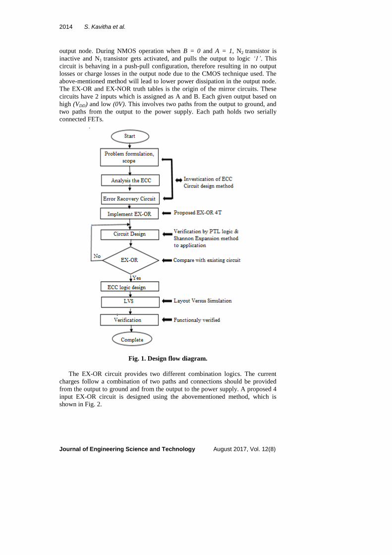
3. Design Method
Several ECC techniques are being used to enhance memory reliability. Among
these, the extended Hamming and odd-weight column codes, which fall into the
single error correction and double error detection (SEC/DED) code category, are
commonly used. These codes consist of two fields; the data or information field
and the check bit or parity bit field. Hamming code is a weight-based code, where
each position of bit is assigned a weight. The data bits are assigned non power of
two weights while the check bits are assigned power of two weights. Error
coverage for a unique subset of information bits is provided by each parity bit.
This information bits is called a parity group [12, 13]. The basis of our work
involves applying the idea of error detection and correction code and improving
this technique for improved performance. The design idea of the ECC circuit is
shown in Fig. 1.
The proposed ECC circuit uses many components such as EX-OR, AND,
MUX and D Flip-Flop circuit. All the above-mentioned combinational circuits are
designed using the Pass Transistor Logic (PTL) concept. The proposed 4-bit EX-
OR gate, the core component of the proposed ECC circuit, was designed using the
dynamic logic technique and consists of 12 transistors. Existing 3T EX-OR and
PTL based EX-OR circuits are used as the benchmark for the purpose of
evaluating the performance of our proposed circuit. The proposed 4-input EX-OR
logic gate is designed based on the push-pull configuration method of CMOS
architecture, which involves the use of voltage controlled circuits. The input
performance is based on the PMOS and NMOS characteristics [14]. If input is
logic ‘0’, both the output and input terminal voltage will be equal to zero. This
state, called the OFF state, can initiate the push-pull of the EX-OR gate. For an
EX-OR circuit, having input A = 0 and B = 0 will result in output being ‘0’. In the
circuit realization, input A goes to the first PMOS source input and second CMOS
gate input. Simultaneously, input B goes to N2 transistor and input A also goes to
N1 transistor. Using this configuration, the output may logically be zero. When
input A = 1, and B = 0, P1 transistor gets activated and gives a logic ‘1’ in the
2014 S. Kavitha et al.
Journal of Engineering Science and Technology August 2017, Vol. 12(8)
output node. During NMOS operation when B = 0 and A = 1, N2 transistor is
inactive and N1 transistor gets activated, and pulls the output to logic ‘1’. This
circuit is behaving in a push-pull configuration, therefore resulting in no output
losses or charge losses in the output node due to the CMOS technique used. The
above-mentioned method will lead to lower power dissipation in the output node.
The EX-OR and EX-NOR truth tables is the origin of the mirror circuits. These
circuits have 2 inputs which is assigned as A and B. Each given output based on
high (VDD) and low (0V). This involves two paths from the output to ground, and
two paths from the output to the power supply. Each path holds two serially
connected FETs.
Fig. 1. Design flow diagram.
The EX-OR circuit provides two different combination logics. The current
charges follow a combination of two paths and connections should be provided
from the output to ground and from the output to the power supply. A proposed 4
input EX-OR circuit is designed using the abovementioned method, which is
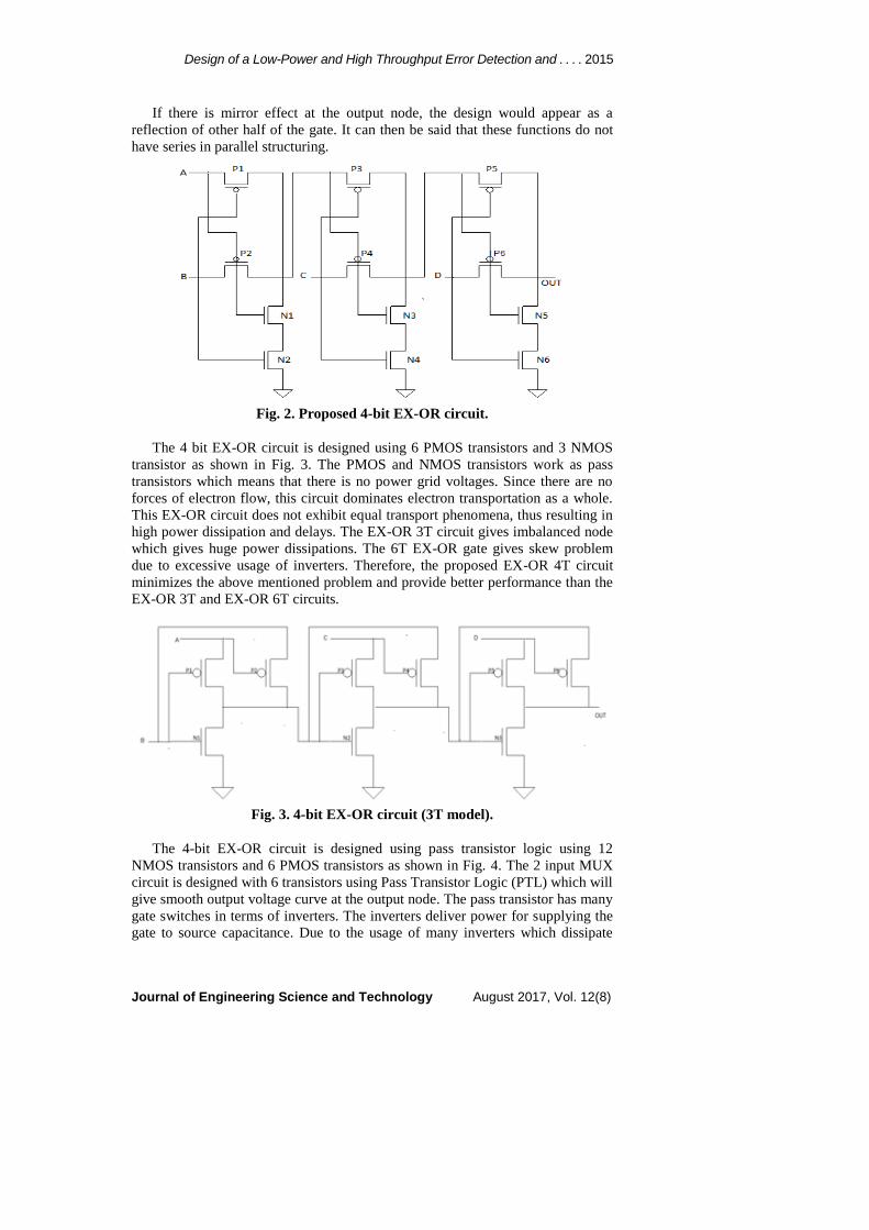
shown in Fig. 2.
Design of a Low-Power and High Throughput Error Detection and . . . . 2015
Journal of Engineering Science and Technology August 2017, Vol. 12(8)
If there is mirror effect at the output node, the design would appear as a
reflection of other half of the gate. It can then be said that these functions do not
have series in parallel structuring.
Fig. 2. Proposed 4-bit EX-OR circuit.
The 4 bit EX-OR circuit is designed using 6 PMOS transistors and 3 NMOS
transistor as shown in Fig. 3. The PMOS and NMOS transistors work as pass
transistors which means that there is no power grid voltages. Since there are no
forces of electron flow, this circuit dominates electron transportation as a whole.
This EX-OR circuit does not exhibit equal transport phenomena, thus resulting in
high power dissipation and delays. The EX-OR 3T circuit gives imbalanced node
which gives huge power dissipations. The 6T EX-OR gate gives skew problem
due to excessive usage of inverters. Therefore, the proposed EX-OR 4T circuit
minimizes the above mentioned problem and provide better performance than the
EX-OR 3T and EX-OR 6T circuits.
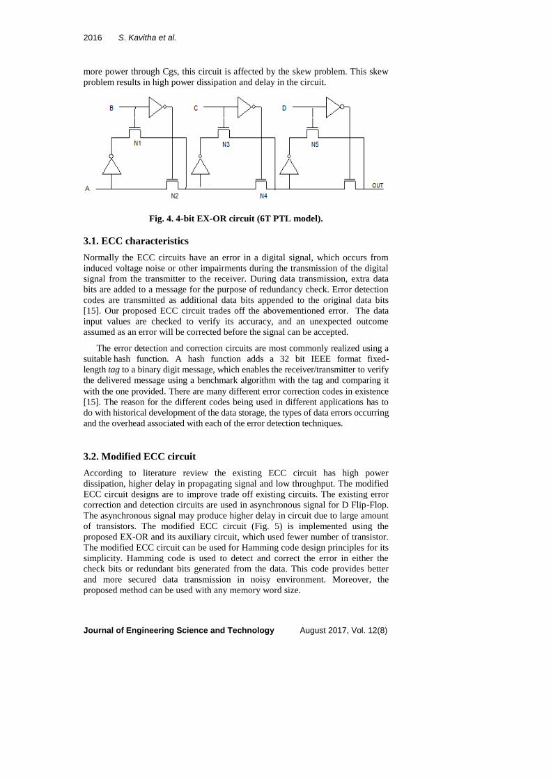
Fig. 3. 4-bit EX-OR circuit (3T model).
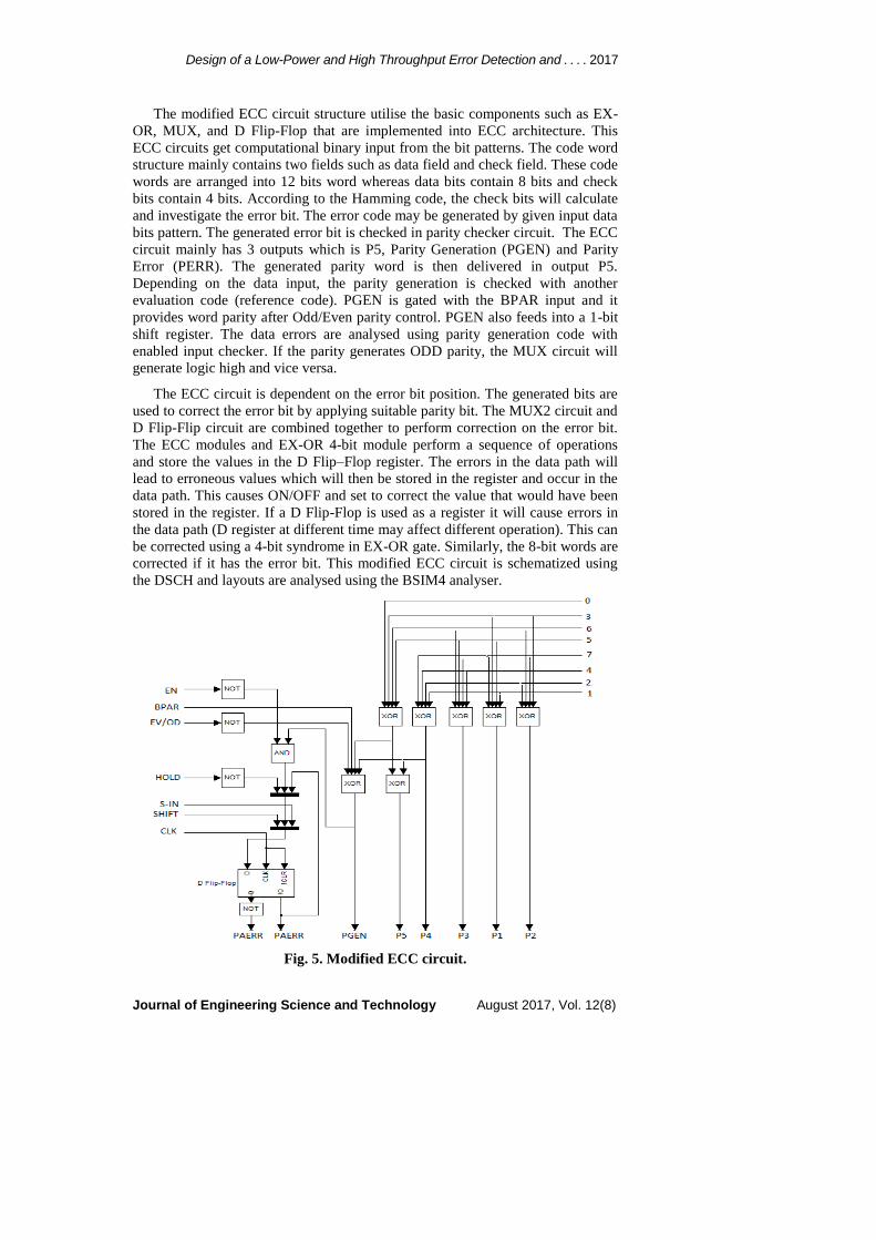
The 4-bit EX-OR circuit is designed using pass transistor logic using 12
NMOS transistors and 6 PMOS transistors as shown in Fig. 4. The 2 input MUX
circuit is designed with 6 transistors using Pass Transistor Logic (PTL) which will
give smooth output voltage curve at the output node. The pass transistor has many
gate switches in terms of inverters. The inverters deliver power for supplying the
gate to source capacitance. Due to the usage of many inverters which dissipate
2016 S. Kavitha et al.
Journal of Engineering Science and Technology August 2017, Vol. 12(8)
more power through Cgs, this circuit is affected by the skew problem. This skew
problem results in high power dissipation and delay in the circuit.
Fig. 4. 4-bit EX-OR circuit (6T PTL model).
3.1. ECC characteristics
Normally the ECC circuits have an error in a digital signal, which occurs from
induced voltage noise or other impairments during the transmission of the digital
signal from the transmitter to the receiver. During data transmission, extra data
bits are added to a message for the purpose of redundancy check. Error detection
codes are transmitted as additional data bits appended to the original data bits
[15]. Our proposed ECC circuit trades off the abovementioned error. The data
input values are checked to verify its accuracy, and an unexpected outcome
assumed as an error will be corrected before the signal can be accepted.
The error detection and correction circuits are most commonly realized using a
suitable hash function. A hash function adds a 32 bit IEEE format fixed-
length tag to a binary digit message, which enables the receiver/transmitter to verify
the delivered message using a benchmark algorithm with the tag and comparing it
with the one provided. There are many different error correction codes in existence
[15]. The reason for the different codes being used in different applications has to
do with historical development of the data storage, the types of data errors occurring
and the overhead associated with each of the error detection techniques.
3.2. Modified ECC circuit
According to literature review the existing ECC circuit has high power
dissipation, higher delay in propagating signal and low throughput. The modified
ECC circuit designs are to improve trade off existing circuits. The existing error
correction and detection circuits are used in asynchronous signal for D Flip-Flop.
The asynchronous signal may produce higher delay in circuit due to large amount
of transistors. The modified ECC circuit (Fig. 5) is implemented using the
proposed EX-OR and its auxiliary circuit, which used fewer number of transistor.
The modified ECC circuit can be used for Hamming code design principles for its
simplicity. Hamming code is used to detect and correct the error in either the
check bits or redundant bits generated from the data. This code provides better
and more secured data transmission in noisy environment. Moreover, the
proposed method can be used with any memory word size.
Design of a Low-Power and High Throughput Error Detection and . . . . 2017
Journal of Engineering Science and Technology August 2017, Vol. 12(8)
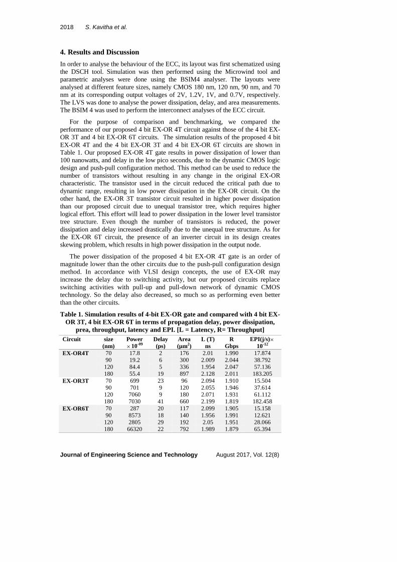
The modified ECC circuit structure utilise the basic components such as EX-
OR, MUX, and D Flip-Flop that are implemented into ECC architecture. This
ECC circuits get computational binary input from the bit patterns. The code word
structure mainly contains two fields such as data field and check field. These code
words are arranged into 12 bits word whereas data bits contain 8 bits and check
bits contain 4 bits. According to the Hamming code, the check bits will calculate
and investigate the error bit. The error code may be generated by given input data
bits pattern. The generated error bit is checked in parity checker circuit. The ECC
circuit mainly has 3 outputs which is P5, Parity Generation (PGEN) and Parity
Error (PERR). The generated parity word is then delivered in output P5.
Depending on the data input, the parity generation is checked with another
evaluation code (reference code). PGEN is gated with the BPAR input and it
provides word parity after Odd/Even parity control. PGEN also feeds into a 1-bit
shift register. The data errors are analysed using parity generation code with
enabled input checker. If the parity generates ODD parity, the MUX circuit will
generate logic high and vice versa.
The ECC circuit is dependent on the error bit position. The generated bits are
used to correct the error bit by applying suitable parity bit. The MUX2 circuit and
D Flip-Flip circuit are combined together to perform correction on the error bit.
The ECC modules and EX-OR 4-bit module perform a sequence of operations
and store the values in the D Flip–Flop register. The errors in the data path will
lead to erroneous values which will then be stored in the register and occur in the
data path. This causes ON/OFF and set to correct the value that would have been
stored in the register. If a D Flip-Flop is used as a register it will cause errors in
the data path (D register at different time may affect different operation). This can
be corrected using a 4-bit syndrome in EX-OR gate. Similarly, the 8-bit words are
corrected if it has the error bit. This modified ECC circuit is schematized using
the DSCH and layouts are analysed using the BSIM4 analyser.
Fig. 5. Modified ECC circuit.
2018 S. Kavitha et al.
Journal of Engineering Science and Technology August 2017, Vol. 12(8)
4. Results and Discussion
In order to analyse the behaviour of the ECC, its layout was first schematized using
the DSCH tool. Simulation was then performed using the Microwind tool and
parametric analyses were done using the BSIM4 analyser. The layouts were
analysed at different feature sizes, namely CMOS 180 nm, 120 nm, 90 nm, and 70
nm at its corresponding output voltages of 2V, 1.2V, 1V, and 0.7V, respectively.
The LVS was done to analyse the power dissipation, delay, and area measurements.
The BSIM 4 was used to perform the interconnect analyses of the ECC circuit.
For the purpose of comparison and benchmarking, we compared the
performance of our proposed 4 bit EX-OR 4T circuit against those of the 4 bit EX-
OR 3T and 4 bit EX-OR 6T circuits. The simulation results of the proposed 4 bit
EX-OR 4T and the 4 bit EX-OR 3T and 4 bit EX-OR 6T circuits are shown in
Table 1. Our proposed EX-OR 4T gate results in power dissipation of lower than
100 nanowatts, and delay in the low pico seconds, due to the dynamic CMOS logic
design and push-pull configuration method. This method can be used to reduce the
number of transistors without resulting in any change in the original EX-OR
characteristic. The transistor used in the circuit reduced the critical path due to
dynamic range, resulting in low power dissipation in the EX-OR circuit. On the
other hand, the EX-OR 3T transistor circuit resulted in higher power dissipation
than our proposed circuit due to unequal transistor tree, which requires higher
logical effort. This effort will lead to power dissipation in the lower level transistor
tree structure. Even though the number of transistors is reduced, the power
dissipation and delay increased drastically due to the unequal tree structure. As for
the EX-OR 6T circuit, the presence of an inverter circuit in its design creates
skewing problem, which results in high power dissipation in the output node.
The power dissipation of the proposed 4 bit EX-OR 4T gate is an order of
magnitude lower than the other circuits due to the push-pull configuration design
method. In accordance with VLSI design concepts, the use of EX-OR may
increase the delay due to switching activity, but our proposed circuits replace
switching activities with pull-up and pull-down network of dynamic CMOS
technology. So the delay also decreased, so much so as performing even better
than the other circuits.
Table 1. Simulation results of 4-bit EX-OR gate and compared with 4 bit EX-
OR 3T, 4 bit EX-OR 6T in terms of propagation delay, power dissipation,
prea, throughput, latency and EPI. [L = Latency, R= Throughput]
Circuit size
(nm)
Power
10-09
Delay
(ps)
Area
(µm2)
L (T)
ns
R
Gbps
EPI(j/s)
10-12
EX-OR4T 70 17.8 2 176 2.01 1.990 17.874
90 19.2 6 300 2.009 2.044 38.792
120 84.4 5 336 1.954 2.047 57.136
180 55.4 19 897 2.128 2.011 183.205
EX-OR3T 70 699 23 96 2.094 1.910 15.504
90 701 9 120 2.055 1.946 37.614
120 7060 9 180 2.071 1.931 61.112
180 7030 41 660 2.199 1.819 182.458
EX-OR6T 70 287 20 117 2.099 1.905 15.158
90 8573 18 140 1.956 1.991 12.621
120 2805 29 192 2.05 1.951 28.066
180 66320 22 792 1.989 1.879 65.394
Design of a Low-Power and High Throughput Error Detection and . . . . 2019
Journal of Engineering Science and Technology August 2017, Vol. 12(8)
The 4 bit EX-OR 4T circuit was compared with the EX-OR 3T and EX-OR
6T circuits in terms of power dissipation, delay, area, latency, throughput and EPI
for feature size 70 nm and its corresponding voltage of 0.7V. In terms of power
dissipation, the EX-OR 4T performed 97.45% and 93.79% better compared with
EX-OR 3T and EX-OR 6T circuits, respectively. The balanced PMOS and
NMOS transistor tree structure gives an equal amount of sharing charges to the
output transistor. In terms of delay, the proposed EX-OR 4T managed to improve
upon the EX-OR 3T and EX-OR 6T by 91.3% and 90%, respectively. This is due
to the fact that the times for the transition of rise and fall are equal. When
comparison is made in terms of area, the proposed EX-OR 4T compared with EX-
OR 3T and EX-OR 6T has improved our circuit 45% and 33% respectively due to
number of transistor reduced in the design approach. Looking at latency, the
proposed EX-OR 4T circuit compared favourably with the EX-OR 3T and EX-
OR 6T by 4% and 4.2%, respectively. Similarly, the EX-OR 4T performed
4.02% and 4.27% better compared to the EX-OR 3T and EX-OR 6T respectively
in terms of throughput. Finally, in terms of Energy Per Instruction, which is value
of the product of toggle capacitance and its output voltage, the proposed EX-OR
4T saw an improvement of 13% and 15% respectively when compared with the
EX-OR 3T and EX-OR 6T circuits.
In addition, the proposed 4 bit EX-OR circuits have shorter switching times.
The charging time constant of series – parallel circuit is given in Eq. (1). The
series-parallel circuit has a constant charging time, whereas the PFETs have been
assumed to be of equal size in resistance and represents the capacitance between
the upper and lower PFET groups.
τp = RpC1 + 2RpCout (1)
The time constant for the low-to-high transition is given in Eq. (4).
τn= RnC2+ 2RnCout (2)
Within the limits of this analysis, the two sides of transistor structure are
symmetrical which results in a much simpler layout. The proposed circuit output
is mainly dependent PGEN. There is an odd function when odd number of 1’s
gives and output equal to 1, with f = 0 otherwise. The proposed EX-OR 4T
sharing connections are used between the output and the power supply (or)
ground. The individual functions can be traced through each branch, while the
circuit may appear somewhat complex at first sight. For example, the right NFET
array directly implements the complement of the terms
dcbcbadcbadcba )....(......
dcba )..( (3)
While the left array gives the complemented form of
dcbadcbadcba ).(......
(4)
Other terms of cross connections are generated in the same manner. The
transient switching times are more complicated to deal with even though the
construction of logic function via FET placement is straightforward. These
functions are provided by Fig. 1 and its time constant related with the charging
circuit is as follows:
2020 S. Kavitha et al.
Journal of Engineering Science and Technology August 2017, Vol. 12(8)
p Cout (Rp1+Rp2 +Rp3 + Rp4+ Rp5 + Rp6) (5)
Similarly, the time constant associated with the discharging path is shown in
Fig. 2.
p Cout (Rn1+Rn2+ Rn3 + Rn4+ Rn5 + Rn6) (6)
These above mentioned Eqs. (5) and (6) ignore parasitic capacitance that are
associated with opposite polarity FETs. This yields switching delay in circuits. In
this proposed circuit, the charging current will revolve around the response time
of the single gate versus a conventional cascaded arrangement. According to the
abovementioned analysis, the delays are measured and shown in Table 1. The
simulated layouts areas are calculated using NMOS FET, PMOS FET aspect
ratios. The total area is calculated via the number of transistor used in the circuit,
input output pad and corresponding connection wires.
4.1. EX-OR based ECC circuit
The 4 input EX-OR based ECC circuit simulation results are shown in Table 2.
The results show that the power dissipation of the circuit is 38nW for CMOS 70
nm feature size. The designed EX-OR gates and other gates are properly arranged
in a dynamic CMOS structure. There is no static power dissipation in the circuit
due to push-pull configuration of the CMOS circuits. So, the circuit avoids
critical path in every input and output patterns. The bit streams are applied to the
circuits as logical ‘1’ and logical ‘0’ concept, which is fed to the modified ECC
circuits. This proposed circuit sends a signal to the output node without any
charge losses due to push-pull configuration and pass transistor configuration.
The power dissipation, delay, area, latency and throughput have achieved their
goals in our proposed circuit due to the abovementioned concept.
Table 2. Simulation results of 4-bit EX-OR 4T,
4-bit EX-OR 3T and 4-bit EX-OR 6T gate based ECC circuit.
Circuit Size
(nm)
Power
10-09
Delay
(ps)
Area
(µm)
L (T)
10-09
T
Gbps
EPI(j/s)
10-12
EXOR4T 70 38 83 1650 2.683 2.981 18.621
90 75 222 1725 3.71 2.156 37.614
120 13 247 2484 4.037 1.981 62.887
180 24200 143 10619 3.036 2.635 186.02
EXOR3T 70 680 15 1335 0.557 0.143 18.847
90 428 55.09 1380 0.894 8.941 39.508
120 2950 56 8970 1.398 5.722 62.258
180 4250 39 8970 1.33 6.015 186.02
EXOR6T 70 18660 20 1536 168.2 0.047 9.795
90 46640
70 1600 0.905 0.088 7.159
120 24990
0.08 2280 0.563 0.141 22.854
180 231500
137 10209 2.4 3.334 90.820
The 4 bit EX-OR 4T circuit is compared with the 4 bit EX-OR 3T and 4 bit
EX-OR 6T ECC circuit in terms of power dissipation, area, delay, throughput,
latency and EPI for feature size 70 nm and its corresponding voltage 0.7V. The
EX-OR 4T has improved the improved the power dissipation by 94.4% and
Design of a Low-Power and High Throughput Error Detection and . . . . 2021
Journal of Engineering Science and Technology August 2017, Vol. 12(8)
99.7% as compared to the EX-OR 3T and EX-OR 6T respectively. This is
probably due to the sub-threshold current that arises from the inversion charges
which exist at the gate voltages below the threshold voltage. The EX-OR 4T as
compared to the EX-OR 3T and EX-OR 6T ECC circuit has an improvement of
81% and 75% respectively in terms of delay due to the minimum average high-
to-low propagation delay and low-to-high propagation delay. The maximum
switching frequency fmax is always equal to 1/2tP, which allows the output
transient of the inverter to be characterized by a RC charge/discharge model.
Our proposed EX-OR 4T as compared to the EX-OR 3T and EX-OR 6T ECC
circuit has improved our design by 19% and 6.9% in terms of area through
advances in circuit design techniques and careful chip layout. The latency of
our proposed EX-OR 4T as compared to the EX-OR 3T and EX-OR 6T ECC
circuit has improved our design by 79% and 98% due to the impact of transistor
parasitic capacitances, wiring capacitance, interconnect capacitance and input
capacitance. The EX-OR 4T as compared to EX-OR 3T and EX-OR 6T ECC
circuit has improved our circuit in terms of throughput by 95% and
98% respectively. Similarly, the EX-OR 4T as compared to the EX-OR 3T and
EX-OR 6T ECC circuit in terms of EPI has improved our circuit by 1.1% and
47% respectively.
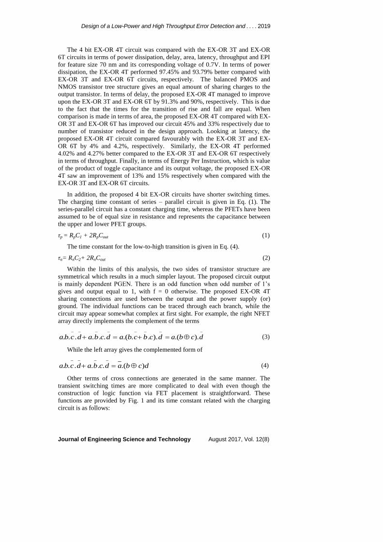
The simulation results of the proposed 4 bit EX-OR 4T based ECC circuits are
shown in Figs. 6, 7 and 8 respectively. The voltage versus time simulation results
is shown Fig. 6 with a feature size of 70 nm.The power dissipation is calculated
using the output power and load power components. In normal operations, the N+
material body is tied to either ground or VDD (if the transistor can be modelled as a
three terminal device). The NMOS switch is turned off when the gate voltage is
below some threshold Vt. The switch turns on forming a channel connecting
source to drain when the gate voltage rises greater than Vt . When the transistor is
in cut off region, Ids is approximately zero. When the transistor is in linear mode,
Ids increases with Vds. In saturation mode, Ids is constant. The PMOS transistor is
similar to NMOS transistor with reversed current flow direction and half of the
current because of lower mobility.
The delay is calculated from its duty cycle of output waveform cycle and is
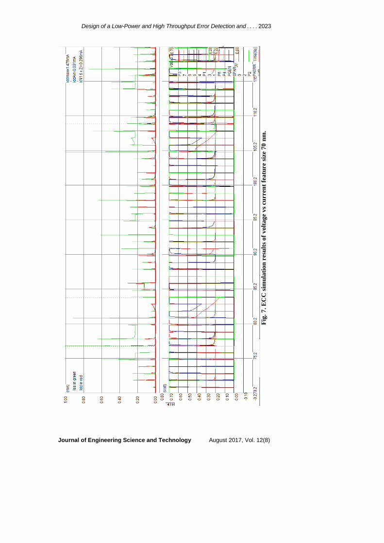
shown in the graph (Fig. 6). The average current of the ECC operation and
corresponding output voltage are indicated in Fig. 7. This graph gives identical
values of output and input voltage.
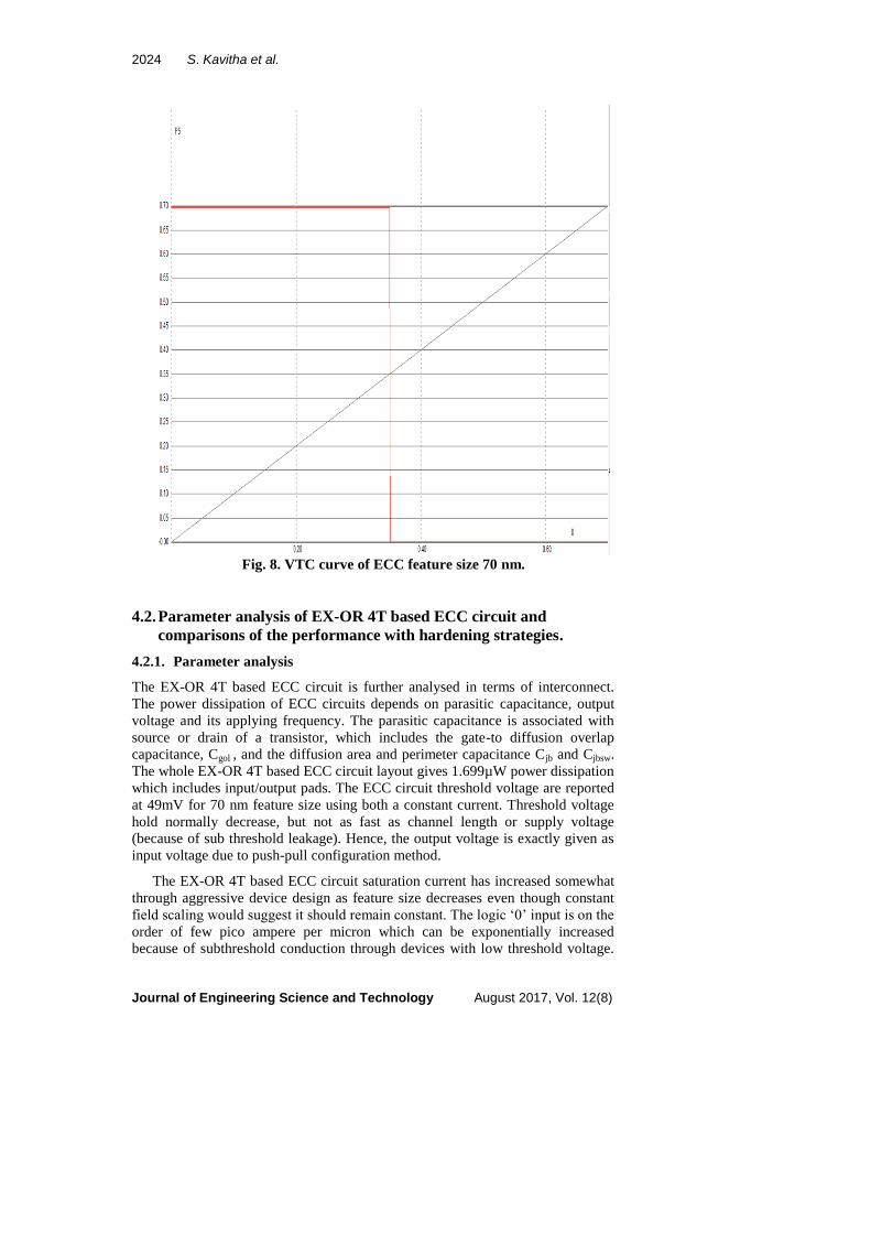
The ECC Voltage Transfer Characteristics (VTC) is shown in Fig. 8, which
is qualitatively similar to that of the ideal inverter transfer characteristic. The
output voltage V is equal to the high value of VOH (output high voltage) because
of the very low input voltage levels. In this case, the driver NMOS transistor is
in interrupt, and hence, does not conduct any current. Accordingly, the output
voltage level is high and the voltage drop across the load device is very small in
magnitude. As the input voltage increases, the driver transistor starts conducting
a certain drain current, and the output voltage eventually starts to decrease. Our
proposed circuit has an ideal VTC characteristic which validates the design. The
circuits are simulated using CMOS 70 nm feature size and 0.7 V for VDD.
According to Fig. 8 the VOH is ~0.69V. According to VTC characteristic the VIH
should be VDD/2 and our circuit gives exactly 0.35V. The VIL is 0.001 and VOL
is 0. The worst-case delay could be calculated using the noise margin formula:
2022 S. Kavitha et al.
Journal of Engineering Science and Technology August 2017, Vol. 12(8)
34.035.069.0 IHOHMH VVN and
001.000.0001.0 OLILML VVN
Fig
. 6
. E
CC
sim
ula
tio
n r
esu
lts
of
vo
lta
ge
vs
tim
e fo
r fe
atu
re s
ize
70
nm
.
Design of a Low-Power and High Throughput Error Detection and . . . . 2023
Journal of Engineering Science and Technology August 2017, Vol. 12(8)
Fig
. 7
. E
CC
sim
ula
tio
n r
esu
lts
of
vo
lta
ge
vs
curr
ent
fea
ture
siz
e 7
0 n
m.
2024 S. Kavitha et al.
Journal of Engineering Science and Technology August 2017, Vol. 12(8)
Fig. 8. VTC curve of ECC feature size 70 nm.
4.2. Parameter analysis of EX-OR 4T based ECC circuit and
comparisons of the performance with hardening strategies.
4.2.1. Parameter analysis
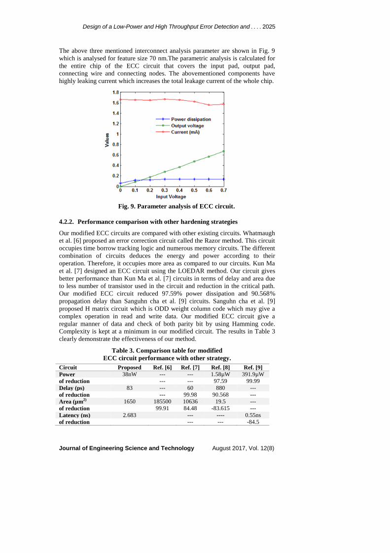
The EX-OR 4T based ECC circuit is further analysed in terms of interconnect.
The power dissipation of ECC circuits depends on parasitic capacitance, output
voltage and its applying frequency. The parasitic capacitance is associated with
source or drain of a transistor, which includes the gate-to diffusion overlap
capacitance, Cgol , and the diffusion area and perimeter capacitance Cjb and Cjbsw.
The whole EX-OR 4T based ECC circuit layout gives 1.699µW power dissipation
which includes input/output pads. The ECC circuit threshold voltage are reported
at 49mV for 70 nm feature size using both a constant current. Threshold voltage
hold normally decrease, but not as fast as channel length or supply voltage
(because of sub threshold leakage). Hence, the output voltage is exactly given as
input voltage due to push-pull configuration method.
The EX-OR 4T based ECC circuit saturation current has increased somewhat
through aggressive device design as feature size decreases even though constant
field scaling would suggest it should remain constant. The logic ‘0’ input is on the
order of few pico ampere per micron which can be exponentially increased
because of subthreshold conduction through devices with low threshold voltage.
Design of a Low-Power and High Throughput Error Detection and . . . . 2025
Journal of Engineering Science and Technology August 2017, Vol. 12(8)
The above three mentioned interconnect analysis parameter are shown in Fig. 9
which is analysed for feature size 70 nm.The parametric analysis is calculated for
the entire chip of the ECC circuit that covers the input pad, output pad,
connecting wire and connecting nodes. The abovementioned components have
highly leaking current which increases the total leakage current of the whole chip.
Fig. 9. Parameter analysis of ECC circuit.
4.2.2. Performance comparison with other hardening strategies
Our modified ECC circuits are compared with other existing circuits. Whatmaugh
et al. [6] proposed an error correction circuit called the Razor method. This circuit
occupies time borrow tracking logic and numerous memory circuits. The different
combination of circuits deduces the energy and power according to their
operation. Therefore, it occupies more area as compared to our circuits. Kun Ma
et al. [7] designed an ECC circuit using the LOEDAR method. Our circuit gives
better performance than Kun Ma et al. [7] circuits in terms of delay and area due
to less number of transistor used in the circuit and reduction in the critical path.
Our modified ECC circuit reduced 97.59% power dissipation and 90.568%
propagation delay than Sanguhn cha et al. [9] circuits. Sanguhn cha et al. [9]
proposed H matrix circuit which is ODD weight column code which may give a
complex operation in read and write data. Our modified ECC circuit give a
regular manner of data and check of both parity bit by using Hamming code.
Complexity is kept at a minimum in our modified circuit. The results in Table 3
clearly demonstrate the effectiveness of our method.
Table 3. Comparison table for modified
ECC circuit performance with other strategy.
Circuit Proposed Ref. [6] Ref. [7] Ref. [8] Ref. [9]
Power 38nW --- --- 1.58µW 391.9µW
of reduction
--- --- 97.59 99.99
Delay (ps) 83 --- 60 880 ---
of reduction
--- 99.98 90.568 ---
Area (µm2) 1650 185500 10636 19.5 ---
of reduction
99.91 84.48 -83.615 ---
Latency (ns) 2.683
--- ---- 0.55ns
of reduction
--- --- -84.5

2026 S. Kavitha et al.
Journal of Engineering Science and Technology August 2017, Vol. 12(8)
5. Conclusion
This paper concisely explained the architecture of a proposed ECC circuit. The
core component of the 4 input EX-OR is proposed and the subsidiary components
are designed for the ECC circuit. The modified ECC circuit and its auxiliary
components are schematized using DSCH and layouts are simulated using the
Microwind CAD tools. The proposed EX-OR 4 transistor circuits would give
enhanced execution results. The modified ECC circuit demonstrates low power
dissipation (94.41%), and high throughput (95.20%) which gives better
performance than existing circuits.
References
1. Ma, K.; and Wu, K. (2011). LOEDAR, A low cost error detection and
recovery scheme for ECC. Proceedings, Design, Automation & Test in
Europe Conference & Exhibition (DATE), 1-6.
2. Brewer, J.; and Gill, M. (2008). Nonvolatile memory technologies with
emphasis on flash. A comprehensive guide to understanding and using flash
memory devices. IEEE Press Series on Microelectronics System, chapter 3,
63-123.
3. Caramia, M.S.; Di Carlo, M.; Fabiano and Prinetto, P. Flare. (2009). A
design environment for flash-based space applications. Proceedings of High
Level Design Validation and Test Workshop. HLDVT 2009. IEEE
International, 14-19.
4. Caramia, M.S.; Di Carlo, M.; Fabiano and Prinetto, P. (2009). Flash-
memories in space applications: Trends and challenges. Proceedings of East-
West Design & Test Symposium (EWDTS), 18-21.
5. Agustin Dominguez-Oviedo.; and Anwar Hasan.M. (2009). Error detection
and fault tolerance in ECSM using input randomization. IEEE Transactions
on dependable and secure computing, 6(3), 175-187.
6. Caramia, M.; Fabiano M.; Miele, A.; Piazza, R; and Prinetto, P. (2010).
Automated synthesis of edacs for flash memories with user-selectable
correction capability. Proceedings of IEEE International on High Level
Design Validation and Test Workshop, HLDVT, 2010, 113-120.
7. Stefano Di Carlo.; Michele Fabiano.; Roberto Piazza.; and Paolo Prinetto.
(2010). EDACs and test integration strategies for NAND flash memories.
Design & Test Symposium (EWDTS), East-West, 218-221.
8. Guo,. X.; Fan, J.; Schaumont, P.; and Verbauwhede, I. (2009). Programmable
and parallel ECC coprocessor architecture: Trade-offs between area, speed
and security, Proceedings. Cryptographic Hardware and Embedded System
(CHES), 289-303.
9. Paul, N.; Whatmough, Shidhartha Das.; and David, M.Bull. (2014). A Low-
power 1-GHz razor FIR accelerator with time-borrow tracking pipeline and
approximate error correction in 65-nm CMOS, IEEE Journal of Solid-State
Circuits, 49(1), 84-94.
10. Kun Ma.; and Kaijie Wu. (2014). Error detection and recovery for ECC: A
new Approach against side-channel attacks. IEEE Transactions on
Computer-Aided Design of Integrated Circuits and Systems, 33(4), 627-637.
Design of a Low-Power and High Throughput Error Detection and . . . . 2027
Journal of Engineering Science and Technology August 2017, Vol. 12(8)
11. Daniel G. T.; Matthieu A.; Fabrice S.; and Michel J. (2014). Soft error
detection and correction technique for radiation hardening based on c-
element and BICS. IEEE Transactions on Circuits and Systems-II: Express
Briefs, 61(12), 952-956.
12. Sanguhn Cha.; and Hongil Yoon. (2012). Efficient implementation of single
error correction and double error detection code with check bit pre
computation for Memories. Journal of Semiconductor Technology and
Science, 12(4), 418-425.
13. Rajkumar, R.; Ramkumar, N.; and Vignesh, M. (2014). An area efficient
error correction codes to protect against stuck-at defects and soft errors.
International Conference on Communication and Signal Processing, India, Melmaruvathur, 2014, 066-070.
14. Neil, H.E.; and Weste David Harris Ayan Banerjee. CMOS VLSI Design.
(Third edition). A Circuits and Systems Perspective.
15. Zarandi, H.R.; Miremadi, S.G.; and A. Ejlali. (2003). Dependability analysis
using a fault injection tool based on synthesizability of HDL models, Proc.
18th IEEE International Symposium Defect Fault Toler. VLSI System, 485-492.
16. Chari, S.N. (2010). Designing a side channel resistant random number
generator. Proceedings of the.9th
International Federation for Information
Processing WG 8.8/11.2 International. Conference. SmartCard Research.
Advanced.Application, 49-64.


![Etu02 Mux Man[1]](https://img.pdfslide.net/doc/110x75/5436e8ae219acd5b118b477c/etu02-mux-man1.jpg)