Embed Size (px)
Citation preview

Design of A Power-Scalable Digital
Least-Means-Square Adaptive Filter
by
Chee We Ng
Submitted to the Department of Electrical Engineering and ComputerScience
in partial fulfillment of the requirements for the degree of
Masters of Engineering in Electrical Engineering and ComputerScience
at the
MASSACHUSETTS INSTITUTE OF TECHNOLOGY
February 2001
c© Chee We Ng, MMI. All rights reserved.
The author hereby grants to MIT permission to reproduce anddistribute publicly paper and electronic copies of this thesis document
in whole or in part.
Author . . . . . . . . . . . . . . . . . . . . . . . . . . . . . . . . . . . . . . . . . . . . . . . . . . . . . . . . . . . . . .Department of Electrical Engineering and Computer Science
December, 2000
Certified by. . . . . . . . . . . . . . . . . . . . . . . . . . . . . . . . . . . . . . . . . . . . . . . . . . . . . . . . . .Anantha Chandrakasan
Associate ProfessorThesis Supervisor
Accepted by . . . . . . . . . . . . . . . . . . . . . . . . . . . . . . . . . . . . . . . . . . . . . . . . . . . . . . . . .Arthur C. Smith
Chairman, Department Committee on Graduate Students
Design of A Power-Scalable Digital Least-Means-Square
Adaptive Filter
by
Chee We Ng
Submitted to the Department of Electrical Engineering and Computer Scienceon December, 2000, in partial fulfillment of the
requirements for the degree ofMasters of Engineering in Electrical Engineering and Computer Science
Abstract
This thesis describes the design of power-scalable digital adaptive equalizer for pulseor quadrature amplitude modulation communication systems, using synthesis andplace-and-route tools. DSP based modem applications such as gigabit Ethernettransceivers require channel equalization. Because of the high rate and computationcomplexity involved, adaptive equalization filters consume a lot of power. Currently,equalization is typically hardwired instead of using a digital signal processor. Yet,there is a need for the equalization filters to be scalable to different channel and bitrate requirements. Synthesis and place-and-route tools enables the designer to focuson higher-level aspects of the design instead of at the transistor level. In this thesis,we have used adaptive tap length and precision techniques to design a digital adaptiveequalizer whose power consumption is scalable to the precision requirements.
Thesis Supervisor: Anantha ChandrakasanTitle: Associate Professor
2

Acknowledgments
To the professors, recitation instructors, and teaching assistants of the 6.00x, 6.01x
introductory Electrical Engineering and Computer Science classes, who taught me to
focus on understanding the fundamentals and gave me the confidence to always seek
out the right answer to questions: Prof. Jeffrey Lang, Prof. Dimitri Antoniadis, Prof.
Alan Willsky, Prof. Clifton Fonstad, Prof. George Verghese, and Andrew Kim.
To Prof. Stephen Senturia, who convinced me doing well in one class is better
than taking seven classes each semester.
To the upperclassmen I knew as a freshmen, who showed me how to get the most
out of MIT.
To the friends, who kept me inspired with their warmth and graciousness.
To our research group, for the help and company.
To particular individuals who helped me tremendously in my thesis, without who
my thesis may not have been completed: Don Hitko and Jim Goodman.
To Prof. Anantha Chandrakasan, for giving me the opportunity to work on this
thesis. I learnt lifelong lessons in perseverance and decisiveness.
To my parents and siblings.
Thank you all.
3

Contents
1 Introduction and Objective 12
1.1 Motivation . . . . . . . . . . . . . . . . . . . . . . . . . . . . . . . . . 12
1.1.1 Low Power Digital CMOS Methodologies . . . . . . . . . . . . 12
1.1.2 A Power-Scalable Least Mean Squares Adaptive Filter . . . . 13
1.2 Thesis Overview . . . . . . . . . . . . . . . . . . . . . . . . . . . . . . 15
2 Overview of Least Mean Squares Adaptive Filters 16
2.1 The Equalizer Problem and the Least Mean Squares Stochastic Gra-
dient Algorithm . . . . . . . . . . . . . . . . . . . . . . . . . . . . . . 16
2.1.1 Fractionally-spaced Decision Feedback Equalizers . . . . . . . 19
2.1.2 Convergence and Stability . . . . . . . . . . . . . . . . . . . . 21
2.1.3 Tap Precision . . . . . . . . . . . . . . . . . . . . . . . . . . . 22
2.1.4 Length of Equalizer . . . . . . . . . . . . . . . . . . . . . . . . 22
2.1.5 Training Sequences and Blind Equalization . . . . . . . . . . . 22
2.2 Previous Work on Low Power Adaptive Decision Feedback Equalizers 23
3 Scalable Adaptive Filter: Signal Processing Issues 27
3.1 Design Overview . . . . . . . . . . . . . . . . . . . . . . . . . . . . . 27
3.1.1 Design Objective . . . . . . . . . . . . . . . . . . . . . . . . . 27
3.1.2 Design Approach . . . . . . . . . . . . . . . . . . . . . . . . . 27
3.2 Fixed Point MATLAB Model . . . . . . . . . . . . . . . . . . . . . . 28
3.2.1 Architecture . . . . . . . . . . . . . . . . . . . . . . . . . . . . 28
3.2.2 Data Representation . . . . . . . . . . . . . . . . . . . . . . . 30
4

3.2.3 Dynamic Range and Precision:
Input, Output, Taps, and Intermediate Results . . . . . . . . . 30
3.2.4 Rounding off Intermediate Results . . . . . . . . . . . . . . . . 32
3.2.5 Simulation Results . . . . . . . . . . . . . . . . . . . . . . . . 32
3.3 Performance of LMS Adaptive Filter . . . . . . . . . . . . . . . . . . 34
3.3.1 Convergence Issues . . . . . . . . . . . . . . . . . . . . . . . . 34
3.3.2 Steady State Output Error, Filter Length and Tap Precision . 35
3.4 Power Consumption of the Baseline LMS Adaptive Filter . . . . . . . 39
3.4.1 Power Dissipation in a Signed Multiplier . . . . . . . . . . . . 40
3.5 Power-Scalable Adaptive Filter Architecture . . . . . . . . . . . . . . 43
4 Scalable Adaptive Filter: Implementation and Results 46
4.1 Overview . . . . . . . . . . . . . . . . . . . . . . . . . . . . . . . . . . 46
4.1.1 Behavioral Description, Simulation, and Synthesis . . . . . . . 47
4.1.2 Preliminary Verification and Power Estimation . . . . . . . . . 48
4.1.3 Place and Route, Incorporating Front-end Cell Views, and Ex-
traction to SPICE . . . . . . . . . . . . . . . . . . . . . . . . 48
4.1.4 Design Verification and Power Estimation . . . . . . . . . . . 48
4.2 Implementation . . . . . . . . . . . . . . . . . . . . . . . . . . . . . . 49
4.2.1 Implementing Adjustable Length . . . . . . . . . . . . . . . . 50
4.2.2 Implementing Adjustable Tap-precision . . . . . . . . . . . . . 50
4.2.3 Control Logic . . . . . . . . . . . . . . . . . . . . . . . . . . . 51
4.2.4 VHDL Description of Filter Structure . . . . . . . . . . . . . . 55
4.3 Results . . . . . . . . . . . . . . . . . . . . . . . . . . . . . . . . . . . 56
4.3.1 Synthesis and Layout . . . . . . . . . . . . . . . . . . . . . . . 56
5 Conclusions and Future Work 59
A Design Documentation:
Scalable Fifteen Tap Adaptive Filter 60
A.1 Top Level . . . . . . . . . . . . . . . . . . . . . . . . . . . . . . . . . 60
5

A.2 Clock-gating . . . . . . . . . . . . . . . . . . . . . . . . . . . . . . . . 63
A.3 Five-tap buiilding block . . . . . . . . . . . . . . . . . . . . . . . . . 64
B Tutorial:
Using the Synthesis and Place-and-Route Design Flow 69
B.1 Basic Synthesis and Layout: An Example . . . . . . . . . . . . . . . . 69
B.1.1 Synthesis . . . . . . . . . . . . . . . . . . . . . . . . . . . . . 69
B.1.2 Place-and-Route . . . . . . . . . . . . . . . . . . . . . . . . . 70
B.2 Extraction . . . . . . . . . . . . . . . . . . . . . . . . . . . . . . . . . 79
B.3 Running Powermill . . . . . . . . . . . . . . . . . . . . . . . . . . . . 81
C Tutorial:
Setting Up the Synthesis and Place-and-Route Design Flow 87
C.1 Data files for CAD Tools . . . . . . . . . . . . . . . . . . . . . . . . . 88
C.2 Setting Up Design Analyzer . . . . . . . . . . . . . . . . . . . . . . . 88
C.3 Setting Up Cadence Silicon Ensemble . . . . . . . . . . . . . . . . . . 89
C.4 Setting up Design Framework . . . . . . . . . . . . . . . . . . . . . . 89
C.5 Setting up Powermill . . . . . . . . . . . . . . . . . . . . . . . . . . . 90
6

List of Figures
1-1 Typical PAM/QAM communications system. . . . . . . . . . . . . . . 13
1-2 Decision-feedback equalizer. . . . . . . . . . . . . . . . . . . . . . . . 14
2-1 Channel impulse response and data sampling points, illustrating Inter-
symbol interference. [Reproduced from [2]] . . . . . . . . . . . . . . . 17
2-2 Least Mean Square Adaptive Filter. . . . . . . . . . . . . . . . . . . . 19
2-3 Decision-feedback equalizer. [Reproduced from [2]] . . . . . . . . . . . 20
2-4 Spectrum of baseband signal input to a FSE and a TSE. . . . . . . . 20
2-5 Two Hybrid Forms of an FIR Filter. [Reproduced from [1]] . . . . . . 23
2-6 An FIR Filter using time-multiplexed multipliers. [Reproduced from [1]] 24
2-7 Measured power per multiplier in FIR filter employing time-multiplexed
Booth recoded multipliers. [Reproduced from [1]] . . . . . . . . . . . 24
2-8 Programmable Gain. [Reproduced from [1]] . . . . . . . . . . . . . . 25
2-9 Power reduction techniques. [Reproduced from [1]] . . . . . . . . . . 25
3-1 Basic six tap LMS adaptive filter. . . . . . . . . . . . . . . . . . . . . 28
3-2 Basic six tap LMS adaptive filter in MATLAB Simulink. . . . . . . . 29
3-3 Simulation of the basic six tap LMS adaptive filter. . . . . . . . . . . 33
3-4 Performance comparison of a infinite precision versus finite precision
filter. . . . . . . . . . . . . . . . . . . . . . . . . . . . . . . . . . . . . 35
3-5 Performance of filter with varying tap length, tap precision and adder
precision, using round-down arithmetic, for ISI over two time samples. 36
3-6 Performance of filter with varying tap length, tap precision and adder
precision, using round-down arithmetic, for ISI over three time samples. 37
7

3-7 Performance of filter with varying tap length, tap precision and adder
precision, using round-to-zero arithmetic, for ISI over two time samples. 38
3-8 Six tap Baseline filter. . . . . . . . . . . . . . . . . . . . . . . . . . . 40
3-9 Power consumption of signed-multipliers of various bit-length given the
same 6-bit input. . . . . . . . . . . . . . . . . . . . . . . . . . . . . . 41
3-10 Comparing using large multipliers for small inputs when inputs are
placed at the least significant and most significant bits. . . . . . . . . 43
3-11 Block diagram of a power-scalable LMS adaptive filter. . . . . . . . . 45
4-1 Overall architecture. . . . . . . . . . . . . . . . . . . . . . . . . . . . 49
4-2 Turning off a block by gating the clocks, reseting the registers, and
latching the input to multipliers. . . . . . . . . . . . . . . . . . . . . 50
4-3 Low-precision mode by gating the clock to the lower precision bit reg-
isters and using lower precision multipliers. . . . . . . . . . . . . . . . 51
4-4 Architecture of control logic. . . . . . . . . . . . . . . . . . . . . . . . 52
4-5 Behavior of Clock-gating Circuit. . . . . . . . . . . . . . . . . . . . . 54
4-6 Clock-gating Circuit. . . . . . . . . . . . . . . . . . . . . . . . . . . . 55
4-7 Layout of Circuit. . . . . . . . . . . . . . . . . . . . . . . . . . . . . . 57
4-8 Trade-off between power and standard deviation of error at output. . 58
B-1 Design Analyzer. . . . . . . . . . . . . . . . . . . . . . . . . . . . . . 70
B-2 Silicon Ensemble Import LEF Dialog. . . . . . . . . . . . . . . . . . . 71
B-3 Silicon Ensemble Import Verilog Dialog. . . . . . . . . . . . . . . . . 72
B-4 Silicon Ensemble Initialize Floorplan. . . . . . . . . . . . . . . . . . . 73
B-5 Silicon Ensemble Place IOs. . . . . . . . . . . . . . . . . . . . . . . . 74
B-6 Silicon Ensemble Place Cells. . . . . . . . . . . . . . . . . . . . . . . 74
B-7 Silicon Ensemble window after placement. . . . . . . . . . . . . . . . 75
B-8 Silicon Ensemble Add Filler Cells. . . . . . . . . . . . . . . . . . . . . 76
B-9 Silicon Ensemble Add Rings. . . . . . . . . . . . . . . . . . . . . . . . 77
B-10 Silicon Ensemble window after routing. . . . . . . . . . . . . . . . . . 78
B-11 Silicon Ensemble Export GDSII. . . . . . . . . . . . . . . . . . . . . . 78
8

B-12 Design Framework Stream In. Click “User-Defined Data” on the left
dialog for the right dialog to appear. . . . . . . . . . . . . . . . . . . 79
B-13 Design Design Framework Virtuoso Layout. . . . . . . . . . . . . . . 80
C-1 Setting up display.drf. . . . . . . . . . . . . . . . . . . . . . . . . . . 90
9

List of Tables
3.1 Representation of input, taps, intermediate results and outputs, and
the normalization needed before the next operator. The representation
p.q means that the integer portion has p bits and the fractional portion
has q bits, and the representation s#r represents that the variable has
s bits, and the actual value the s-bit integer multiplied by 2−s . . . . 31
3.2 Examples of channel responses . . . . . . . . . . . . . . . . . . . . . . 35
3.3 Critical path delays. . . . . . . . . . . . . . . . . . . . . . . . . . . . 40
3.4 Breakdown of power dissipation. Total power consumption is 6.16 mW. 41
3.5 Breakdown of capacitances. . . . . . . . . . . . . . . . . . . . . . . . 41
3.6 Comparison of power consumption of a 10 by 11 bit multiplier versus
a 10 by 16 bit multiplier given the same set of 10 bit and 11 bit inputs,
at a clock frequency of 100MHz. . . . . . . . . . . . . . . . . . . . . . 42
3.7 Representation of input, taps, intermediate results and outputs, and
the normalization needed before the next operator. . . . . . . . . . . 45
4.1 CAD Tools in a digital design flow . . . . . . . . . . . . . . . . . . . 46
4.2 A digital design flow . . . . . . . . . . . . . . . . . . . . . . . . . . . 47
4.3 Control signals for each sub-block. When the sub-block is turned off,
all clock signals are gated, and resets are set high. . . . . . . . . . . . 49
4.4 Critical path delays. . . . . . . . . . . . . . . . . . . . . . . . . . . . 56
4.5 Breakdown of power dissipation (mW) for scalable 15 tap filter. . . . 56
4.6 Breakdown of capacitances(pF) for scalable 15 tap filter. . . . . . . . 57
C.1 Versions of CAD tools . . . . . . . . . . . . . . . . . . . . . . . . . . 87
10

C.2 Data Files Required for CAD Tools . . . . . . . . . . . . . . . . . . . 88
11

Chapter 1
Introduction and Objective
1.1 Motivation
In recent years, power consumption in digital CMOS has become an increasingly
important issue. In portable applications, a major factor in the weight and size of the
devices is the amount of batteries, which is directly influenced by the power dissipated
by the electronic circuits. For non-portable devices, cooling issues associated with the
power dissipation has caused significant interest in power reduction.
1.1.1 Low Power Digital CMOS Methodologies
Several general low-power techniques for digital CMOS have been developed [5, 6,
15, 24, 33, 38, 22]. In [5], power reduction schemes for circuit, logic, architecture
and algorithmic levels were proposed. At the circuit and logic level, these techniques
include transistor sizing, reduced-swing logic, logic minimization, and clock-gating to
power-down unused logic blocks. At the architecture level, optimization techniques
include dynamic voltage scaling and pipelining to maintain throughput, minimizing
switching activity by a careful choice of number representation, and balancing sig-
nal paths. At the algorithm level, these techniques include reducing the number of
operations, and using algorithmic transformations.
In the area of low power filter design, some of the techniques that have been
12

explored include the following. In [22] and [24], the idea of having the overall system
select, during run time, the number of stages required for a filter was introduced
and later demonstrated in [38]. [23] and [28] describe low-power FIR techniques
using algebraic transformations. [33] describes an energy efficient filtering approach
using bit-serial multiplier-less distributed arithmetic technique. [7] and [9] describes
low-power FIR techniques based on differential coefficients and input, and residue
arithmetic respectively.
1.1.2 A Power-Scalable Least Mean Squares Adaptive Filter
In this thesis, the system design of a power-scalable least means square (LMS)
adaptive filter is described. LMS adaptive filters are used for channel equaliza-
tion in modems and transceivers, which are becoming increasing important. These
transceivers require channel equalization because channels tend to disperse a data
pulse and cause Inter-Symbol Interference (ISI). Causes of dispersion include reflec-
tions from impedance mismatches in coaxial cables, filters in voiceband modems and
scattering in radios.
Figure 1-1: Typical PAM/QAM communications system.
Figure 1-1 shows the block diagram of a typical Pulse/Quadrature Amplitude
Modulation (PAM/QAM) system. At the transmitter, the digital data stream is
modulated into band-limited pulse shapes by a pulse shaping filter, shifted to the
carrier frequency by a mixer, and sent through the channel. At the receiver, the
received signal shifted down to baseband, sampled, passed through a matched filter,
and an optimum decision slicer and decoder. PAM and QAM systems can have
13

adjustable bit rates by varying the number of levels of the pulse height from 2(in
anti-podal signaling) to any power of 2. QAM systems pack a higher data rate than
PAM systems by modulating data streams on a set of two orthogonal waveforms –
the in-phase and quadrature components. The reader is refered to texts such as [29]
and [2] for further explanation of these two communication systems.
Figure 1-2: Decision-feedback equalizer.
One of the commonly used equalizer is a decision-feedback equalizer [29], depicted
in Figure 1-2. It consists of a feed-forward section and a feedback section. The feed-
forward section attempts to remove precursor ISI and the feedback section attempts
to remove post-cursor ISI. Both sections use the least-means-square adaptive filter
algorithm [16]. Note that the difference between a decision-feedback equalizer for
QAM and PAM is that the input streams for QAM are complex numbers and the
multiplication and addition operations are complex, instead of real numbers.
Because of the high rate and computation complexity involved, adaptive equal-
ization filters consumes a lot of power. Currently, equalization is typically hardwired
instead of using a digital signal processor because of the large number of operations
required per second. [20] cites a requirement of 1440 million operations per second
14

for a decision feedback equalizer. Current DSPs are capable of about 500 million
operations per second. Yet, there is a need for the equalization filters to be scalable
to different channel and bit rate requirements.
1.2 Thesis Overview
In this thesis, we have used an adaptive tap length and precision technique to make the
power-consumption of a digital adaptive equalizer scalable to the precision require-
ments. Our design is a least-means-square (LMS) adaptive filter that can be used for
a PAM communication system. Designing it for PAM simplifies our study to focus on
one real stream instead of two real streams, and to have a single real multiplier per
tap, as opposed to four in a simple implementation of complex multiplication. The
evaluation system is a PAM system with ISI.
We have used synthesis and place-and-route tools for this design because they en-
able the designer to focus on higher-level aspects of the design instead of the transistor
level.
In the following chapter, I will give an background overview of LMS adaptive
filters and some recent implementations in Chapter 2.
In Chapter 3, I will discuss the signal processing issues involved in designing a
power-scalable adaptive filter, such as in designing a fixed point MATLAB model and
in choosing the precision of intermediate results. We will discuss some simulations to
study the power dissipation patterns of a base-line equalizer and of two’s complement
signed-multipliers, and the performance of the LMS filter as tap precision and length
is reduced.
In Chapter 4, we will discuss the actual implementation of a power-scalable LMS
filter and our findings.
Finally, we conclude with a chapter on suggestions of future work.
15

Chapter 2
Overview of Least Mean Squares
Adaptive Filters
This chapter gives an overview of Least Means Squares (LMS) adaptive filters, and
previous work on low-power implementations.
2.1 The Equalizer Problem and the Least Mean
Squares Stochastic Gradient Algorithm
Assuming that the channel frequency response is well-known and fixed in time, the
pulse shaping filter and matched filter in a QAM/PAM communication system can
be designed so that it satisfies the Nyquist Criterion for no ISI. However in many
communications systems, particularly in wireless applications, the channel is time
varying. Time-varying dispersion moves the zero crossings which are originally located
at the centers of all other symbols. Figure 2-1 shows a channel impulse response and
the data sampling points, illustrating ISI for a PAM system. The largest data sample
is used as a cursor to recover the original data, and the other samples are considered
to be ISI. The samples that come before the cursor are called “precursor ISI” and
those that come after are called “post-cursor ISI”. The role of the channel equalizer
is to perform inverse filtering of the channel impulse response.
16

Figure 2-1: Channel impulse response and data sampling points, illustrating Inter-symbol interference. [Reproduced from [2]]
The equalizer [2] works in the following way. For the sake of discussion, consider
a Finite Impulse Response (FIR) equalization filter. Denote the filter taps as c =
[c[0], c[1], c[2], ...c[N − 1]]� and the impulse response matrix H defined as
hi,j =
h[i − j + 1] for 1 < i − j + 1 < M ,
0 otherwise.(2.1)
where M is the length of the sampled impulse response truncated. The ideal equalizer
should satisfy the following equation
H · c = d (2.2)
where d is the ideal impulse response, i.e. [..0, 0, 1, 0, 0, ...]�. Note that this set of
equations is over-determined. Therefore, it must be solved approximately, either by
zero-forcing or Least Mean Squares (LMS).
The mean square error is given by
|ε|2 = ε�ε = (c�H� − d�) · (Hc− d)
= c�H�Hc− d�Hc − c�H�d + d�d(2.3)
A value of c can be derived analytically to minimize the mean square error by com-
pleting the squares
|ε|2 = (c� − d�H(H�H)−1) · H�H · (c − (H�H)−1H�d)
−d�H(H�H)−1H�d + d�d(2.4)
17

The optimal filter taps is then
copt = H�HH�d (2.5)
Iterative adaptation to this solution can be achieved by the method of steepest de-
scent. The new tap values are calculated from the old values by
c′ = c − ∆d|ε|2
dc= c − ∆2H�(Hc− d) (2.6)
∆ is known as the step size. H and d are not observable. However, if continuous data
is used, we note that
H�H = E[Y�Y] and H�d = E[Y�a] (2.7)
where a is the data stream vector (assumed to be memoryless) and Y is the input
signal (to the equalizer) matrix defined as
yi,j = y[i − j + 1] (2.8)
Hence for a continuous data stream, the new taps are typically computed according
to
ck+1 = ck + ∆εky�k (2.9)
where the subscriptions represent time intervals and yk is the kth row of Y and is
the input signal contents of the FIR at time kT and
εk = d − Hc (2.10)
is the expected output minus the output of the filter. In a more commonly used
notation, this is
cj [k + 1] = cj[k] + ∆ε[k]y[k − j] (2.11)
where cj[k] is the jth tap at time kT . This is known as the LMS stochastic gradient
18

method. This kind of filter is also known as a linear equalizer. Figure 2-2 shows a
block diagram of the filter.
e[k] e[k] e[k]
y[k]
e[k]
a[k]
delta delta delta delta
c [k] c [k] c [k] c [k]0 1 2 N-1
Figure 2-2: Least Mean Square Adaptive Filter.
The discussion so far is for PAM. For QAM, we treat the data streams as com-
plex numbers, where the in-phase stream is represented by the real part and the
quadrature-phase is represented by the imaginary part. The derivation remains the
same if we replace the transpose operator with the hermitian operator.
2.1.1 Fractionally-spaced Decision Feedback Equalizers
In modern communication systems, one of the commonly used equalizer is a decision-
feedback equalizer [29], depicted in Figure 2-3. It consists of a feed-forward section
and a feedback section. The feed-forward section attempts to remove precursor ISI
and the feedback section attempts to remove post-cursor ISI. The decision-feedback
equalizer differs from a linear equalizer in that the feedback filter contains previously
detected symbols, whereas in the linear equalizer the filter contains the estimates.
It has been suggested that a higher performance can be achieved if the equalizer
runs at a smaller spacing than the symbol interval [21, 31, 12]. This can be done by
sampling (refer to Figure 1-1) the received signal at a higher rate than the symbol
rate. This is known as Fractionally-Spaced Equalizers (FSE). Equalizers at symbol
rate will henceforth be called symbol-rate(T-spaced) equalizer (TSE).
It is known that FSE is able to realize matched filtering and equalization in one
device [12]. In addition, while the TSE is very sensitive to sampling phase, the FSE
19

Figure 2-3: Decision-feedback equalizer. [Reproduced from [2]]
Figure 2-4: Spectrum of baseband signal input to a FSE and a TSE.
20

is able to compensate for it. This can be understood by considering the baseband
signal in the frequency domain. This is illustrated in Figure 2-4. The baseband signal
is band-limited to to [−1/2T, 1/2T ] after Nyquist Pulse shaping. T-spaced sampling
causes aliasing at the band edge, so the equalizer can only act on the aliased spectrum,
not the baseband signal itself. Fractionally-spaced sampling, for example at half the
symbol period (T/2), allows the equalizer to act on the baseband signal itself.
2.1.2 Convergence and Stability
The convergence rate, steady state mean square error and stability of the LMS
Stochastic Gradient equalizer is determined by the step size ∆ in equation (2.11).
The results are summarized here and the reader is referred to [2, 29, 11, 30] for
details.
To ensure convergence for all sequences, the step size must be bounded by
∆max <2
Nλmax
(2.12)
where N is the length of the filter and λmax is the largest eigenvalue of H�H the
auto-correlation matrix of the channel. Convergence rate is maximized by a step size
of
∆0 =1
N(λmin + λmax)(2.13)
The final mean square error is given by
ε2∞ =
ε2min
1 − ∆Nλmax/2(2.14)
Fractionally spaced equalizers have a additional stability problem that is described
in [10]. FSE instability is due to the received signal spectrum being zero in the
frequency intervals (1+α)/2T < |f | < 1/2T ′ where T is the symbol interval, α is the
roll-off factor of the Nyquist pulse, and T ′ is the fractional spacing of the equalizer
taps. Thus, the equalizer transfer function is not uniquely determined and tap-weights
can drift and take very large values. Various solutions have been suggested, such as
21
Tap-leakage [10] and others [37, 19, 18].
2.1.3 Tap Precision
The effect of tap precision on the LMS algorithm is explored in [11] and reviewed in
[30]. Adaptation will stop when
∆ε < 2−B (2.15)
where each coefficient is represented over the range of -1 to 1 by B bits including the
sign and the PAM signal yk is assumed to have unit power [2]. The step size required
for the final mean square error can be calculated from equation (2.14), i.e.
∆ =2(1 − ε2
min/ε2∞)
Nλmax(2.16)
The precision required for the taps are then
B = − log2(∆ε) (2.17)
2.1.4 Length of Equalizer
The previous subsection shows that the equalizer length N affects the optimum
step size and precision. For TSE, there are some heuristics for the choice of filter
length [36]. These heuristics suggest that the equalizer length need to be three to
five times the length of the delay spread of the channel which varies from channel to
channel. However, an analysis of the FSE using the zero-forcing criterion seems to
suggest that the FSE need not be longer than delay spread of the channel. Further
simulations in [36] reveal that the minimum filter order needed for a symbol error
rate of 10−6 does not correlate with estimates of the channel delay spread.
2.1.5 Training Sequences and Blind Equalization
The adaptation of filter coefficients in equation (2.11) is based on an assumed correct
decision about which symbol was received. This is true for equalizers with a training
22
sequence. However for blind equalizers, the decision is not necessary correct. We will
not look into these issues, which are dwelt in [2, 13, 39]. It suffice to say that our
design should be made as flexible as possible.
2.2 Previous Work on Low Power Adaptive Deci-
sion Feedback Equalizers
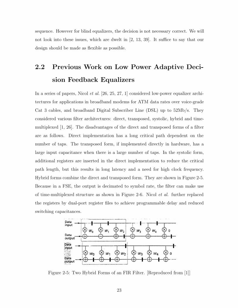
In a series of papers, Nicol et al. [26, 25, 27, 1] considered low-power equalizer archi-
tectures for applications in broadband modems for ATM data rates over voice-grade
Cat 3 cables, and broadband Digital Subscriber Line (DSL) up to 52Mb/s. They
considered various filter architectures: direct, transposed, systolic, hybrid and time-
multiplexed [1, 26]. The disadvantages of the direct and transposed forms of a filter
are as follows. Direct implementation has a long critical path dependent on the
number of taps. The transposed form, if implemented directly in hardware, has a
large input capacitance when there is a large number of taps. In the systolic form,
additional registers are inserted in the direct implementation to reduce the critical
path length, but this results in long latency and a need for high clock frequency.
Hybrid forms combine the direct and transposed form. They are shown in Figure 2-5.
Because in a FSE, the output is decimated to symbol rate, the filter can make use
of time-multiplexed structure as shown in Figure 2-6. Nicol et al. further replaced
the registers by dual-port register files to achieve programmable delay and reduced
switching capacitances.
Figure 2-5: Two Hybrid Forms of an FIR Filter. [Reproduced from [1]]
23
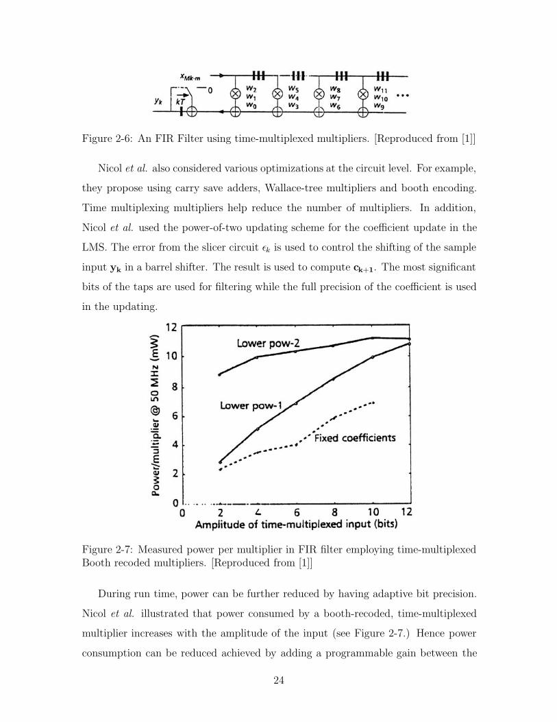
Figure 2-6: An FIR Filter using time-multiplexed multipliers. [Reproduced from [1]]
Nicol et al. also considered various optimizations at the circuit level. For example,
they propose using carry save adders, Wallace-tree multipliers and booth encoding.
Time multiplexing multipliers help reduce the number of multipliers. In addition,
Nicol et al. used the power-of-two updating scheme for the coefficient update in the
LMS. The error from the slicer circuit εk is used to control the shifting of the sample
input yk in a barrel shifter. The result is used to compute ck+1. The most significant
bits of the taps are used for filtering while the full precision of the coefficient is used
in the updating.
Figure 2-7: Measured power per multiplier in FIR filter employing time-multiplexedBooth recoded multipliers. [Reproduced from [1]]
During run time, power can be further reduced by having adaptive bit precision.
Nicol et al. illustrated that power consumed by a booth-recoded, time-multiplexed
multiplier increases with the amplitude of the input (see Figure 2-7.) Hence power
consumption can be reduced achieved by adding a programmable gain between the
24

Figure 2-8: Programmable Gain. [Reproduced from [1]]
filter and the slicer as shown in Figure 2-8. This gain can be limited to power of 2
for simplicity.
Further power reduction can be achieved by having burst-mode update and adap-
tive filter lengths. In burst-mode update, as long as the mean square error stays below
a certain level, the update section is frozen. Filter lengths are adaptively changed to
achieve a given performance. Tail taps are usually small, thus setting them to zero
will not significantly change the transfer function. When a tap is disabled, it is not
updated and it is replaced by 0. The delay line still needs to operate because other
non-zero taps still need to be updated.
Figure 2-9: Power reduction techniques. [Reproduced from [1]]
Figure 2-9 shows a cumulative benefits of each power reduction approach described
by Nicol et al..
25

A second series of work is done by Shanbag et al. [32, 14]. In [32], they described
a reconfigurable filter architecture with a variable power supply voltage scheme and
a coefficient update block that shuts off certain taps according to an optimal trade
off between power consumption and mean square error. Taps with small values of
|cj|2/E(cj) where cj is the filter coefficient and E denotes the energy. When taps are
shut down, the critical path length is reduced, and the supply voltage can be reduced
to further reduce power. Additional power savings can be achieved by changing the
precision of the input signal and the coefficients. This is done by forcing the least
significant bits to zero. Note the difference between this approach and that taken by
Nicole et al.
In [14], Shanbag et al. described algebraic transformations for low-power. By
reformulating the algebraic expression so that it has more additions and fewer multi-
plications than before, the power consumption can be reduced because multiplication
are more expensive not only in terms of power but area as well. This is known as
strength reduction. The DFE for QAM shown in Figure 1-2 requires complex multi-
plications. This allows strength reduction methods to be easily used. Shanbag et al.
suggests that this method has a potential of up to 25% power savings.
The second optimization considered in [14] is pipelining with relaxed lookahead.
Essentially this method allows the adders in the LMS algorithm to be pipelined by
applying a lookahead in time domain. Thus throughput of the LMS is increased. To
achieve low-power, one can reduce the power supply, for example.
A third set of work is done by Samueli et al.[17, 35, 20]. In these papers, Sammueli
et al. studied algebraic transformation and relaxed lookahead pipelining techniques
that enable power-supply voltage to be reduced, while maintaining the same through-
put.
26

Chapter 3
Scalable Adaptive Filter: Signal
Processing Issues
This chapter describes the signal processing issues in the design of a scalable LMS
adaptive filter.
3.1 Design Overview
3.1.1 Design Objective
The goal of the design in this thesis is an LMS adaptive filter that is able to trade off
power-dissipation and quality of its computation in real time using the same piece of
hardware. The quality of its computation is measured by the standard deviation of the
error on the output, after sufficiently long time has been allowed for the adaptation
to converge.
3.1.2 Design Approach
The filter will be scalable in two aspects:
1. The length of the filter will be adjustable in real time.
2. The tap-precision will be adjustable in real time.
27

3.2 Fixed Point MATLAB Model
We begin our discussion on the signal processing issues with an fixed point model of
a six tap adaptive filter.
3.2.1 Architecture
Figure 3-1 shows a six tap adaptive filter and Figure 3-2 show its implementation in
MATLAB Simulink using the fixed-point library.
e[k] e[k] e[k] e[k] e[k]
y[k]
e[k]
a[k]
Taps Taps Taps Taps Taps Taps
Dt1 Dt2 Dt3 Dt4 Dt5
Tap Multiplier Sum
Tap UpdateMultiplier
Tap Update
Figure 3-1: Basic six tap LMS adaptive filter.
The basic structure consists of
1. five 10-bit registers labeled “Dt1” to “Dt5” for the delay line,
2. six 10-bit registers labeled “Taps” for the taps,
3. six multipliers labeled as “Tap Multiplier” to form the tap products,
4. five adders shown as labeled “Sum” to form the sum of the products,
5. six multipliers labeled “Tap Update Multiplier” for to compute the coefficient
update, and
6. six adders labeled “Tap Update” to add the update to the previous tap.
The inputs and taps have 10 bit precision. Precision issues will be in the next section.
Note that in simulink, variables can be multiplexed to form a vector, and multiplica-
tion and addition operators act component by component if two vectors are presented
at the input of the operator.
28

0.03125
step sizeS10 2^−14
Out
int2f8
Out
int2f6
Out
int2f5
Out
int2f2
Out
int2f1
In
f2int1S10 2^−7
In
f2int 2S10 2^−7
Waveform
User
Taps Display
1
z
TapsTapUpdate
S12
Tap UpdateMultiplierS19
Tap MultiplierS21
SumS8
Sign
0.00048828
Normalize 2S7
0.00048828Normalize 1S12
Display and Vector GenerationEvaluating System: PAM
Basic Six Tap LMS Adaptive Filter Integer Model
0.0039062
IntegerToFix 2S10 2^−8
0.0625
IntegerToFixS8 2^−5
[VecErr]
Goto9
[VecOut]
Goto8
[DispErr]
Goto7
[DispOut]
Goto6
[DispTx]
Goto5
[DispRx]
Goto4
[Err]
Goto3
[Taps]
Goto2
[In]
Goto11
[VecIn]
Goto10
[Out]
Goto1
[VecErr]
From9
[VecIn]
From8
[DispOut]
From7
[DispErr]
From6
[DispTx]
From5 [DispRx]
From4
[Taps]
From3
[Out]
From2
[In]
From11
[VecOut]
From10
[Err]
From1
basic.mat
For Test VectorGeneration
4096
FixtoIntegerS10
128
Fix/I 1S10
1
z
Dt5
1
z
Dt4
1
z
Dt3
1
z
Dt2
1
z
Dt1
DMS Source
DF2T
Channel ISI
2b.8b
3b.7b
3b.4b3b.4b
3b.4b
3b.7b
3b.7b
In
Received
Transmitted
Error
Output from Filter
Figure 3-2: Basic six tap LMS adaptive filter in MATLAB Simulink.
29

The noteworthy components of the MATLAB model are the “normalizing” gain
elements, labeled “Normalize 1” and “Normalize 2”. These elements extract the
significant digits of the previous computation and throws away the less significant
digits. The decision of how much precision to maintain for intermediate results is
important and will be discussed in a later section.
The coefficient update is calculated according to equation 2.11. The gain element
labeled “step size” is the step size ∆ for the adaptation as discussed in section 2.1.
In this design, ∆ = 2−5 can be easily implemented by shifts without the use of
multipliers.
The evaluating system is a simple PAM communication system with inter-symbol
interference (ISI). The “transmitter” is a two-level discrete memoryless source. The
ISI of the channel is modeled in simulink using “Direct Form II Transpose Filter”.
Since we know at the “receiver” end what the transmitted symbols are, we can easily
compute the error stream for the LMS filter.
3.2.2 Data Representation
The filter uses data represented in two’s-complement. While two’s complement ad-
dition of signed integers requires no modification from unsigned addition, signed
multiplication is significantly different from unsigned multiplication [8]. There are
various kinds of multipliers that can be chosen, including array, Wallace-tree and
booth-encoded. We have chosen to use the Synopsys synthesis default, which is two’s
complement. This thesis does not attempt to compare the trade-offs between the
various representations, and the arithmetic blocks used.
3.2.3 Dynamic Range and Precision:
Input, Output, Taps, and Intermediate Results
In implementing a fixed-coefficient digital filter in hardware, with a given the spec-
ification of the input and output dynamic range and bit precision, the designer can
determine the precision of the intermediate results and design for worst case. In an
30

adaptive filter, because the taps are adapted, we need to set a dynamic range for the
taps. It is conceivable that for a set dynamic range in a design, a worst case scenario
can be devised so that the taps will overflow. This is a very catastrophic situation
for the adaptive filter algorithm [10].
In this implementation, I have chosen to think about the variables as fixed point
numbers and represent them in the form P.Q where P represents the integer part and
Q represents the fractional part. For example, I have chosen the inputs to be 10 bits,
with 3 bits representing the integer portion, and 7 bits representing the fractional
part. Hence the binary representation 0100000001 is interpreted as 010.0000001 and
equals 2 127 . Since we are using two’s-complement, note the most significant bit of the
binary representation is the sign bit. We also note that although the position of the
“decimal point” of all the variables in the filter can be shifted together by the same
amount without changing the functionality, it is convenient to fix the position of the
“decimal point” for an arbitrary variable. An alternative way of keeping track of the
position of the “decimal point” is as follows. The fixed point number is multiplied by
the smallest power of two 2S until it becomes an integer R. We must keep track of S
for all intermediate results.
Table 3.1: Representation of input, taps, intermediate results and outputs, and thenormalization needed before the next operator. The representation p.q means that theinteger portion has p bits and the fractional portion has q bits, and the representations#r represents that the variable has s bits, and the actual value the s-bit integermultiplied by 2−s
Variable Representation Normalization neededInput 3.7 or 10#7 -Taps 2.8 or 10#8 -Result of “Tap Multiplier” 5.15 or 20#15 Discard two most significant
and eleven least significant bitsGain of “Normalize 2” = 2−11
Input to Sum 3.4 or 7#4Error εk 3.7 or 10#7∆εk 10#12 -Result of “Tap Update 1.19 or 20#19 Discard eleven least significant bitsMultiplier” and sign-extend 2 bits
Gain of ”Normalize 1” = 2−11
31

Table 3.1 summarizes the representation and precision of the inputs, taps, inter-
mediate results, and the outputs. In the table, the representation p.q means that the
integer portion has p bits and the fractional portion has q bits, and the representa-
tion s#r represents that the variable has s bits, and the actual value the s-bit integer
multiplied by 2−s. p.q represents the same thing as p + q#q.
Note that when two numbers with the precision p1.q1 is multiplied by another p2.q2,
the result has the precision (p1 + p2).(q1 + p2). When two numbers with the precision
r1#s1 is multiplied by another r2#s2, the result has precision (r1 + r2)#(s1 + s2).
3.2.4 Rounding off Intermediate Results
Because multiplication increases the bit length after each operation, full precision
cannot be carried throughout the entire filter. In this implementation, we have cho-
sen to round down instead of rounding to zero because of ease of implementation.
Rounding down of a number represented in two’s complemented can be easily done
by truncating the lower order bits. However, using rounding down has a significant
impact on the performance of the filter, which we will discuss in the following chapter.
It is important to note that “rounding down” must be specified in the gain elements
in the MATLAB model as “Round toward: Floor” for generating the appropriate test
vectors.
3.2.5 Simulation Results
Figure 3-2 shows the simulation of the basic six tap LMS adaptive filter in MATLAB
simulink for a sampled channel impulse response of h[n] = 1 + 0.6z−1.
The first plot shows the data transmitted, and the second shows how it inter-
symbol interference after the data has gone through the channel. The third plot
shows the output from the LMS adaptive filter as it adapts its coefficients, and the
fourth shows the difference between the transmitted and the filtered signal.
32

−2
−1
0
1
2Transmitted
−2
−1
0
1
2Received
−2
−1
0
1
2Output from Filter
0 50 100 150 200 250 300 350 400−2
−1
0
1
2Error
Time offset: 0
Figure 3-3: Simulation of the basic six tap LMS adaptive filter.
33

3.3 Performance of LMS Adaptive Filter
3.3.1 Convergence Issues
Having studied the performance of a six tap filter, we proceed to investigate the
performance of a finite length and a finite precision LMS filter.
From the discussion in section 2.1.4, there is no known correlation between the
tap length required for a small error rate and the delay spread. Our first simulation
attempts to investigate the effect of having a finite length filter, and a finite precision
finite length filter.
The simulation set up is as follows. A Simulink model for a 20-tap LMS adaptive
filter with a step size of 2−5 is set up. It is run with a set of randomly generated
channel impulse responses:
h[n] =a0δ[n] + a1δ[n − 1] + a2δ[n − 2]√
a20 + a2
1 + a23
(3.1)
where a0=1, a1 and a2 are uniformly generated random numbers between 1 and -1.
The denominator is to “normalize” the energy of the channel response. The data
we collect is the mean-square-error of the output after some time has been given for
convergence.
The same experiment is repeated with a finite precision 20-tap filter, with a tap
precision of 16 bits, inputs, outputs, and final sum of 10-bits.
Note we do not attempt to replicate any real channel in this investigation. Our
goal is to study the limitations of a finite length filter, and the effect of having finite
precision. We will then identify a set of channel impulse response converges with a
finite-length filter, and study the trade off between tap length, and precision, and the
mean square error at the output.
Figure 3-4 shows the frequency distribution of the standard deviation of the error
(expected-output) for a infinite precision and finite precision 20-tap filter. Note that
even for a channel response that has two samples of post-cursor ISI, the finite-length
infinite-precision filter does not converge satisfactory and still has over 48% of the
34

0 0.5 1 1.5 2 2.5 30
10
20
30
40
50
60
Standard Deviation Error
Fre
quen
cy
20−Tap Finite Precision Filter
0 0.5 1 1.5 2 2.5 30
10
20
30
40
50
60
Standard Deviation Error
Fre
quen
cy
20−Tap Infinite Precision
Figure 3-4: Performance comparison of a infinite precision versus finite precision filter.
simulated channel responses that has a error standard deviation of greater than 0.1.
We note that the finite precision filter have a similar performance, with the exception
that it experiences overflow and becomes unstable for some channel responses.
Table 3.2: Examples of channel responsesBehavior Channel responseConverge 0.88282 − 0.1415z−1 + 0.447890z−2
to error std dev <0.1 0.85715 + 0.40270z−1 + 0.32113z−2
Does not converge 0.82922 − 0.37904z−1 − 0.41075z−2
0.74100 + 0.54183z−1 − 0.39666z−2
Causes tap overflow 0.67690 + 0.39913z−1 + 0.61847z−2
0.74744 + 0.56169z−1 + 0.35474z−2
Table 3.2 shows a snap shot of the channel responses that converges, does not
converge, or causes tap-overflow. Note that there does not seem to be any discernible
pattern why some converges, some do not, and some causes tap overflow.
3.3.2 Steady State Output Error, Filter Length and Tap Pre-
cision
Given the set of channel impulse response that will converge with 20 tap filter, we
proceed to see the effects of shortening the filter, and reducing the precision of the
taps.
35

0 5 10 15 20 25−3
−2.5
−2
−1.5
−1
−0.5
0
log 10
std
(err
or)
Number of Taps
Final Sum bits=10
10 Tap Bits11 Tap Bits12 Tap Bits16 Tap Bits
0 5 10 15 20 25−3
−2.5
−2
−1.5
−1
−0.5
0
log 10
std
(err
or)
Number of Taps
Final Sum bits=12
10 Tap Bits11 Tap Bits12 Tap Bits16 Tap Bits
0 5 10 15 20 25−3
−2.5
−2
−1.5
−1
−0.5
0
log 10
std
(err
or)
Number of Taps
Final Sum bits=16
10 Tap Bits11 Tap Bits12 Tap Bits16 Tap Bits
Figure 3-5: Performance of filter with varying tap length, tap precision and adderprecision, using round-down arithmetic, for ISI over two time samples.
36

0 5 10 15 20 25−3
−2.5
−2
−1.5
−1
−0.5
0
log 10
std
(err
or)
Number of Taps
Final Sum bits=10
10 Tap Bits11 Tap Bits12 Tap Bits16 Tap Bits
0 5 10 15 20 25−3
−2.5
−2
−1.5
−1
−0.5
0
log 10
std
(err
or)
Number of Taps
Final Sum bits=12
10 Tap Bits11 Tap Bits12 Tap Bits16 Tap Bits
0 5 10 15 20 25−3
−2.5
−2
−1.5
−1
−0.5
0
log 10
std
(err
or)
Number of Taps
Final Sum bits=16
10 Tap Bits11 Tap Bits12 Tap Bits16 Tap Bits
Figure 3-6: Performance of filter with varying tap length, tap precision and adderprecision, using round-down arithmetic, for ISI over three time samples.
37

0 5 10 15 20 25−3
−2.5
−2
−1.5
−1
−0.5
0
log 10
std
(err
or)
Number of Taps
Final Sum bits=10
10 Tap Bits11 Tap Bits12 Tap Bits16 Tap Bits
0 5 10 15 20 25−3
−2.5
−2
−1.5
−1
−0.5
0
log 10
std
(err
or)
Number of Taps
Final Sum bits=12
10 Tap Bits11 Tap Bits12 Tap Bits16 Tap Bits
0 5 10 15 20 25−3
−2.5
−2
−1.5
−1
−0.5
0
log 10
std
(err
or)
Number of Taps
Final Sum bits=16
10 Tap Bits11 Tap Bits12 Tap Bits16 Tap Bits
Figure 3-7: Performance of filter with varying tap length, tap precision and adderprecision, using round-to-zero arithmetic, for ISI over two time samples.
38

Using 3 channel responses, we simulated the performance of the filter with varying
tap length, tap precision and adder precision. Figure 3-5 shows plots the standard
deviation of the error as tap length, tap precision and adder precision is varied.
Refering to the top left graph in Figure 3-5, we make the following observations.
First, given the number of taps, and the precision of the final sum, a higher tap
precision leads to a smaller error and better performance. Second, a larger number
of taps may lead to poorer performance, especially with low precision taps (10,11
and 12). Finally, comparing the three graphs in Figure 3-5, we observe that the
precision of the final sum only improves the performance of the filter when the taps
have high-precision (in this case 16 bits).
When we performed performed the same experiment with ISI that covers three
time samples as shown in Figure 3-6, we found that a larger number of taps led to
better performance most of the time.
When we performed the same simulation with round-toward-zero instead of round-
down, the performance of the filter is better, as shown in Figure 3-7. Surprisingly, it
is much less dependent on the tap precision, except when the precision of the sum is
high.
3.4 Power Consumption of the Baseline LMS Adap-
tive Filter
The power consumption of a baseline six tap filter in Section 3.2 is estimated using
Powermill. The precision of the input, taps, intermediate results and outputs were
discussed in Table 3.1 and summarized in Figure 3-8. Since the LMS algorithm
computes the next tap based on the difference between the current computed output
and its expected value, (see equation 2.11) the critical path is from the input a to
the tap register, through the output y and the external operation that computes
the difference between y and its expected value, and feeds that back as err. Using
the results in Table 3.3, assuming that the computation of err requires no time,
39

the maximum clock rate estimated by Synopsys, using a conservative delay model is
17.19+6.21
GHz=74.6 MHz.
Table 3.3: Critical path delays.From To Time (ns)a[3] (input) y[6] (output) 7.19err[2] (error input) taps reg[1][9] (tap register) 6.21
We found correct functionality when clocked at 100MHz. With a power supply
of 1.8 volts, the average power consumption is 6.16 milliwatts. The break-down of
the power dissipation is shown in Table 3.4. Since we can reduce power consumption
in general by decreasing power supply voltage and clock frequency, a more useful
metric is to consider the total switched capacitance. The total switched capacitance
is calculated using
C =P
fV 2dd
(3.2)
and equals 19.00 pF. Table 3.5 shows the break down of switched capacitances. We
noted that the total switched capacitance of the clock has the same value as the
extracted SPICE netlist.
e[k] e[k] e[k] e[k] e[k]
y[k]
e[k]
a[k]
Taps Taps Taps Taps Taps Taps
Dt1 Dt2 Dt3 Dt4 Dt510
10
10
7
10
10
Figure 3-8: Six tap Baseline filter.
3.4.1 Power Dissipation in a Signed Multiplier
In this simulation, we investigate if it is sufficient just to wire the lower-order bits
of the inputs to a signed-integer multiplier to zero, if we want to conserve power
dissipation by using lower precision taps.
40

Table 3.4: Breakdown of power dissipation. Total power consumption is 6.16 mW.Element PercentageClock 1.95Delay line registers 4.78Tap registers 5.68Tap update multiplier 27.37Tap update adder 11.11Tap multiplier 35.21Final sum 13.89
Table 3.5: Breakdown of capacitances.Element pFClock 0.36Delay line registers 0.91Tap registers 1.08Tap update multiplier 5.20Tap update adder 2.11Tap multiplier 6.69Final sum 2.64
6 7 8 9 10 11 12 13 14 15 160
0.5
1
1.5
2
2.5
3
3.5
4
4.5
5
bits
pow
er [m
W]
using most−significant bits using least−significant bits
6 7 8 9 10 11 12 13 14 15 160
5
10
15
bits
capa
cita
nce
[pF
]
using most−significant bits using least−significant bits
Figure 3-9: Power consumption of signed-multipliers of various bit-length given thesame 6-bit input.
41

Using Synopsys, we synthesized 6, 8, 12 and 16-bit two’s-complement signed mul-
tipliers. The multipliers were simulated with inputs from a set of 6-bit uniformly
generated random numbers. For the 8, 12, and 16-bit multiplier, the 6-bit numbers
were placed in the 6 most-significant bits as well as in the 6 least-significant bits (refer
to Figure 3-10) When clocked at 100 MHz, with a power-supply of 1.8V, the power
consumption, and the total switched capacitance is graphed in Figure 3-9. The results
show that in the design of a variable tap-precision filter, using the same multiplier
wastes unnecessary power even when the lower-order bits are zeroed. In this case,
the power dissipation of a bigger multiplier is bigger because of glitching within the
multiplier. In the case of using the least-significant bits of a multiplier, the power
dissipation is even greater. This is because the multipliers are two’s complement
multipliers, so all the higher order bits need to switch when computing the sign and
the magnitude of the result.
In the power-scalable filter design to be discussed in the following section, we will
allow tap precision to vary in real time. Table 3.6 compares the power dissipation of
a 10 by 11 bit multiplier versus a 10 by 16 bit multiplier (using the most-significant
bits) given the same set of uniformly distributed 10 bit and 11 bit inputs. By using
two different multipliers, when the tap precision changes from 16 to 11, 11% of the
energy dissipation can be saved1.
Table 3.6: Comparison of power consumption of a 10 by 11 bit multiplier versus a10 by 16 bit multiplier given the same set of 10 bit and 11 bit inputs, at a clockfrequency of 100MHz.
10 by 11 bit 10 by 16 bitAverage power [mW] 1.53 1.72Total switched capacitance [pF] 4.72 5.31
1In our design, we have chosen not to vary the precision of the delay line, as we shall see in thenext section. If we chose to vary the precision of the delay line, we would get greater power savings.
42

6
6
A[5:0]
B:[5:0]
6
6
6
6
6
6
0
0
0
0
0
0
B[5:0]
A[9:0]
B[9:0]B[1:0]
A[1:0] A[5:0]
6 6 6
666
B[11:6]
A[7:2] A[11:6] A[15:10]
B[15:10]B[7:2]
A[7:6]
B[7:6]
A[5:0]
B[5:0]
A[11:6]
B[11:6]
A[5:0]
B[5:0]
A[15:6]
B[15:6]
A[5:0]
B[5:0]s[5]
s[5] s[5]
s[5] s[5]
s[5]
Using least significant bits (s[5] performs sign-extension)
Using most significant bits
Figure 3-10: Comparing using large multipliers for small inputs when inputs areplaced at the least significant and most significant bits.
3.5 Power-Scalable Adaptive Filter Architecture
Our simulation shows that the major sources are power are the multipliers, followed
by the adders and the registers.
This suggest that we should use burst-mode update of the coefficients, and use
power-of-two update. This finding is similar to Nicol et al. [26, 25, 27, 1] as discussed
in section 2.2
In addition to dissipating less energy when not needed, we saw that a shorter
length can sometimes lead to a smaller standard deviation of error at the output.
We will focus this thesis on making the filter power-scalable. Our findings suggest
that significant power can be saved if number of taps and the precision can be varied
when necessary.
The design in this thesis will have four levels of adjustability:
1. Level 0 : Five 11-bit taps
2. Level 1 : Ten 11-bit taps
3. Level 2 : Ten 16-bit taps
4. Level 3 : Fifteen 16-bit taps
43

We have chosen to keep the precision of the delay line constant for this design. We
could have reduced the precision of the delay line and this would have given us greater
power dissipation reduction.
Based on this discussion, we came up with the following fifteen-tap adaptive filter
architecture. Figure 3-11 shows the block diagram of the design. It consists of three
5-tap LMS adaptive filter blocks. Each filter block accepts three inputs: 10-bit input
a[k], 10-bit error input e[k], and a 10-bit sum y′[k] from another block. The output
y[k] is the sum of y′[k] and the convolution computed in that block. Each filter block
also outputs a delayed a[n] for the next block. Note that this is simply dividing a
15-tap filter into 3 sections. The three sections are not exactly identical. The first
section contains only 4 register banks for the delay line because the first tap does
not require a register. The second and third all have 5 register banks. The final
filter block does not require to have to have a input y′[n] from another block, so it
saves one adder as well. This implementation allows us to shut down the latter two
blocks when only 5 or 10 taps are required. In addition, within each block, we can
adjust the precision of the taps. We will discuss the implementation of adjustable
tap precision in the next chapter. The precision of inputs, taps, intermediate results,
and output summarized in Table 3.7. Here we have chosen to increase the tap and
output precision from the six tap filter discussed in the beginning of the chapter.
44

e[k]e[k]e[k]e[k]e[k]
a[k]
y[k]
e[k]
a[k]
y[k]
e[k]
a[k]
y[k]
e[k]
a[n-9]
y3[n]
a[n-4]
y2[n]
a[n]
e[n]
y[n]
y[k-5]
y’[k]
y[k-4]
y’[k]
y[k]
a[k] a[k-5]
y’[k]10
7
11 or 16
11 or 16
10
10
Figure 3-11: Block diagram of a power-scalable LMS adaptive filter.
Table 3.7: Representation of input, taps, intermediate results and outputs, and thenormalization needed before the next operator.Variable Representation Normalization neededInput 3.7 or 10#7 -High Precision Taps 2.14 or 16#14 -Low Precision Taps 2.9 or 11#9 -Result of “Tap Multiplier”High Precision 5.21 or 26#21 Discard two most significant
and fourteen least significant bitsGain of “Normalize 2” = 2−14
Low Precision 5.16 or 21#16 Discard two most significantand nine least significant bitsGain of “Normalize 2” = 2−9
Input to Sum 3.7 or 10#7Error εk 3.7 or 10#7∆εk 10#12 -Result of “Tap Update 1.19 or 20#19 Discard eleven least significant bitsMultiplier” and sign-extend 2 bits
Gain of ”Normalize 1” = 2−11
45

Chapter 4
Scalable Adaptive Filter:
Implementation and Results
4.1 Overview
This section describes the implementation process in this thesis. The CAD tools
used in the design flow are: Synopsys Design Analyzer, Cadence Silicon Ensemble,
Cadence Design Framework II, Cadence Dracula, and EPIC Powermill. The function
of these tools is summarized in Table 4.1.
Table 4.1: CAD Tools in a digital design flowTool FunctionSynopsys VHDL Debugger Behavioral description and simulationSynopsys Design Analyzer Behavioral synthesis using standard-cell libraries
Static Timing AnalysisCadence Silicon Ensemble Automatic place-and-route using standard-cell
front-end viewsCadence Design Framework Integrating back-end cell views with placement
and routingCadence Dracula Extraction to SPICE netlist for back-annotationEPIC Powermill Design functionality and timing verification
Power estimation
The steps in our design flow is summarized in Table 4.2 and will be described in
the following subsections. The scope and organization of this section is as follows.
46

It will summarize the steps of the flow but the detailed commands for each tool will
be described in Appendix B (using a simpler example). Appendix C will explain the
process of setting up of the cell libraries and the technology files for the tools.
Table 4.2: A digital design flowInput Step Output
1. Design architecture Behavioral description VHDL descriptionTest vectors and simulation
2. VHDL description Logic synthesis Structural Verilog netlistStandard-cell back-end views
3. Verilog netlist from synthesis Preliminary verification Power estimationStandard-cell CDL netlist and power estimation
4. Verilog netlist from synthesis Place and route Placed-and-routed designSilicon Ensemble abstract views in GDSII without
front-end views5. GDSII file from place-and-route Incorporating Full layout in Design
Standard-cell front-end views front-end views Framework6. Full layout in GDSII Design-rule check SPICE netlist
Verilog netlist from synthesis and extraction with annotationStandard-cell CDL netlistDracula rules
7. SPICE netlist from extraction Verification Power estimationTest vectors and power-estimationSPICE Models
4.1.1 Behavioral Description, Simulation, and Synthesis
The first step in implementation is to translate the integer model design into VHDL
description. In this thesis, we have chosen a mixture of behavioral and structural
VHDL, to simplify the process of implementing adders and multipliers. The VHDL
description is first verified with VHDL Debugger using the test vectors from the
MATLAB model, and a test bench written in VHDL. Finally, the VHDL description
is then synthesized using Design Analyzer. The standard-cell back-end views is needed
for design analyzer. The result from this step is a Verilog netlist containing structural
instantiations of the standard-cells. From the synthesized schematic, Synopsys can
perform static timing analysis of the critical path.
47

4.1.2 Preliminary Verification and Power Estimation
Using Epic Powermill, we can perform an initial verification of the functionality and
perform a power estimation. Because the Verilog netlist from synthesis retains its
hierarchical nature, we can perform power analysis of individual blocks in the filter:
the multipliers, adders and registers. This step requires the SPICE or CDL (a SPICE-
like but Cadence proprietary) netlist of the standard-cells which are provided by
the standard-cell provider for Layout-Versus-Schematics (LVS) checks. Powermill
provides a utility vlog2e which will compile the Verilog netlist and standard-cell netlist
into an Epic proprietary format that can be used in Powermill.
4.1.3 Place and Route, Incorporating Front-end Cell Views,
and Extraction to SPICE
The next step is to place and route the Verilog netlist. Using an abstract view contain-
ing information of pin location (places in a standard-cell that the router contacts to),
Silicon Ensemble places and routes the netlist. The design can be saved as a GDSII
(stream) file. This is imported to Cadence Design Framework, where the complete
front-end views of each cell has been loaded into a library. In the process of import-
ing, Cadence automatically incorporates the cell views of each standard-cell into the
design. Following this, we perform extraction to SPICE netlist for back-annotation.
The files required for Dracula to perform the last step are the CDL netlist for the
standard-cells and the LPE (layout parasitic extraction) rules, in addition to the
Verilog netlist from synthesis.
4.1.4 Design Verification and Power Estimation
Finally, with a SPICE netlist, we can perform final design verification and power
estimation. This is done using Epic Powermill. The SPICE models for the devices
are required by Powermill in this step.
48

4.2 Implementation
This section describes the actual implementation of the fifteen tap scalable adaptive
filter. Figure 4-1 shows the overall architecture. As discussed in the previous section,
e[k]e[k]e[k]e[k]e[k]
y[k]
a[k] a[k-5]
y’[k]
y[9:0]
a[9:0]
err[9:0] err[9:0] err[9:0]clk lclk rst lrst clk lclk rst lrst clk lclk rst lrst
level[1:0]
clkControl
4 4 4
11 or 16
10
7
10
10
11 or 16
Figure 4-1: Overall architecture.
the filter has four levels of adjustability which is encoded in the level signal. The
filter consists of three sub-blocks, which are controlled by the control block. The
function of the control signal to each sub-block is summarized in Table 4.3 and will
be explained in the following subsections.
Table 4.3: Control signals for each sub-block. When the sub-block is turned off, allclock signals are gated, and resets are set high.
Signal Functionclk clock for the block except the least-significant tap bitslclk clock for the least-significant tap bitsrst asynchronously resets all registers except the least-
significant tap bitslrst asynchronously resets all the least-significant tap bits
activates low-precision mode for the sub-block
49

4.2.1 Implementing Adjustable Length
To shut off the latter two filter blocks when not needed, we have chosen to gate the clk
signal of those blocks. For these blocks not to consume significant power when turned
off, the inputs to the tap-update multiplier must be latched, since the err[9 : 0] is still
changing. In addition, all the registers are asynchronously reset so that when these
blocks are restarted, they do not contain any old values. The latter two behavior is
implemented by having a rst signal to tell the sub-block when the latches should hold
and the registers should be reset. Figure 4-2 summarizes this implementation.
e[k]e[k]e[k]e[k]e[k]
y[k]
a[k] a[k-5]
y’[k]
rst
e[k]
reset when block is turned off latch input to multiplier when block is turned off
reset when block is turned off
rst
clk
rst
clk
Figure 4-2: Turning off a block by gating the clocks, reseting the registers, andlatching the input to multipliers.
4.2.2 Implementing Adjustable Tap-precision
The second aspect of scalability is the tap-precision. We shutdown the bits in the
tap registers when they are not being used by gating the clock. lclk is the clock for
50

the lower-order tap bits that is gated by the control block when the filter is running
in low-precision. This is shown in Figure 4-3
In addition, we employ a simple bit-length adjustable multiplier to conserve power
when running in low-precision mode. The simple bit-length adjustable multiplier is
shown in Figure 4-3. It consists of two multipliers of different input bit-length. When
e[k]e[k]e[k]e[k]e[k]
y[k]
a[k] a[k-5]
y’[k]
[15:0]
[15:5]
lrst
[9:0]
16x10 11x10
rst
clk
[15:5]
lrst
[4:0]
lclk
lrst 1
lrst
0
Use a smaller multiplier when low-precission mode is on
reset the lower bits when low-precision mode is on
Figure 4-3: Low-precision mode by gating the clock to the lower precision bit registersand using lower precision multipliers.
a higher precision is needed, the longer bit-length multiplier is turned on and the
inputs to the other is latched so they are not affected by the inputs.
4.2.3 Control Logic
The control logic performs two functions. First, it decodes the level[1 : 0] signal into
a signal for whether each block should be turn on or off (shut), and whether each
block should be running high tap precision mode or low tap precision mode (lowpre).
Second, the control logic translates this into the clk, lclk, rst, and lrst signals for
51

each sub-block. This is summarized in Figure 4-4
clk rst
level[1:0]
e[k]e[k]e[k]e[k]e[k]
y[k]
a[k] a[k-5]
y’[k]
y[9:0]
a[9:0]
err[9:0] err[9:0] err[9:0]clk lclk rst lrst clk lclk rst lrst clk lclk rst lrst
level[1:0]
clkControl
4 4 4
shut
clock-gatinglowpre
decode
clock-gating
clk rst
rst1
lclk1
lrst1
clk1
Figure 4-4: Architecture of control logic.
The first portion is a simple combinational logic that computes the shut and
lowpre signal for each sub-block. The second portion is slightly more elaborate be-
cause we allow the level[1 : 0] signal to be asynchronous. Hence the clock-gating logic
must only start gating gclk and setting rst high at the next suitable time.
The clock-gating logic works as follows. It takes a clk, rst, and shut signal and
derives a inverted clk and rst signal for a filter sub-block when shut is is low. When
shut goes high, derived clock is held high at the subsequent rising clk edge. It is held
high until the first rising clk edge after shut goes low again. During the time between
the missed clock edges, the reset of the sub-blocks are held high to reset the internal
registers and to latch the inputs to the tap-update multiplier.
The following VHDL code describes the behavior of the clock-gating circuit.
Figure 4-5 illustrates the behavior of the clock-gating circuit. The example shows
the shut signal going high at 35ns, and the derived clock, ngclk, is held high at the
next rising edge of the original clock, clk. The derived clock, ngclk, is gated until
the rising edge of the clk following shut going low, which happens at 55ns and 45ns
respectively. During the missing edges of ngclk, the derived reset, nrst is held low.
Figure 4-6 shows the schematic for the clock-gating circuit. Note that in this
implementation, glitching is avoided in ngclk because glitches can only happen when
52

entity tapctrl is
port( clk: in std_logic; -- clock and reset of the entire circuit
rst: in std_logic;
shut: in std_logic; -- a signal for shutting a particular block
ngclk: out std_logic; -- inverted clock that is generated
grst: out std_logic); -- reset signal that is generated
end tapctrl;
architecture behavior of tapctrl is
signal shutn,shutp,nshut: std_logic;
begin
process(clk,shut) begin
if rising_edge(clk) then
shutp<=shut;
end if;
end process;
process(rst,clk,shut) begin
if rst=’1’ then
shutn<=’0’;
elsif falling_edge(clk) then
shutn<=shut;
end if;
end process;
grst<=(shutn and shutp) or rst;
nshut<=not shutn;
ngclk<=not(clk and nshut);
end behavior;
53

Figure 4-5: Behavior of Clock-gating Circuit.
54

clk is ’1’ and shutn is transitioning. However, shutn only transitions when register
R2 is clocked, i.e. at the falling edge of clk. Clock-skew is minimized by having the
same clock-gating circuit for each block.
Q
rstQ
D
D
clk
shut
rst
Q
ngclk
grst
shutn
shutp
R2
R1
Figure 4-6: Clock-gating Circuit.
4.2.4 VHDL Description of Filter Structure
The filter is described using behavioral VHDL. The full code is listed in Appendix A.
The design is done hierarchically, according to Figure 3-11. For each five-tap filter
block, the signals involved are first defined in the architecture section, and then then
the relationship between them respect to the clock is described. The regular structure
of the FIR filter enables the use of arrays easily. The code makes use of the Design
Analyzer to synthesize the signed-integer adders and multipliers. Normalization is
implemented by writing a loop to “shift the index of the array”. Particular attention
is drawn to sign-extension. This happens in the adder for the tap coefficient update.
While the tap itself may be large in magnitude, the update is often small, so sign
extension is needed so that both inputs to the adder has the same number of bits.
The sign-extension is required was discussed in Table 3.1
55

4.3 Results
4.3.1 Synthesis and Layout
The design is synthesized and laid out.
Using the design analyzer command “report timing”, the maximum delay from
the input to the output, and from the error input to the tap registers are summarized
in Table 4.4. Since the LMS algorithm computes the next tap based on the difference
between the current computed output and its expected value, (see equation 2.11) the
critical path is from the input a to the tap register, through the output y and the
external operation that computes the difference between y and its expected value, and
feeds that back as err. Using the results in the table, assuming that the computation
of err requires no time, the maximum clock rate estimated by Synopsys, using a
conservative delay model is 19.72+6.28
GHz=62.5 MHz.
Table 4.4: Critical path delays.From To Time (ns)input y[9] (output) 9.72err[0] (error input) taps reg[4][15] (tap register) 6.28
The final layout has a transistor count of 117,315 and dimensions of 743µm by
773µm in 0.18µm technology, excluding the pads. Figure 4-7 shows the layout in
Cadence. When clocked at 33MHz with a power supply of 1.8 volts, the power
consumption is summarized in Tables 4.5 and 4.6.
Table 4.5: Breakdown of power dissipation (mW) for scalable 15 tap filter.Element Level 0 Level 1 Level 2 Level 3
5 11-bit Taps 10 11-bit Taps 10 16-bit Taps 15 16-bit TapsClock 0.06 (0.9%) 0.13 (1.1%) 0.19 (1.3%) 0.27 (1.3%))Delay line registers 0.12 (1.9%) 0.26 (2.3%) 0.26 (1.8%) 0.40 (1.8%)Tap registers 0.12 (1.9%) 0.23 (2.2%) 0.35 (2.3%) 0.53 (2.3%)Update multiplier 2.25 (35.0%) 3.85 (34.0%) 3.45 (23.0%) 4.21 (18.4%)Tap update adder 0.50 (7.7%) 0.94 (8.3%) 1.34 (8.9%) 1.86 (8.1%)Tap multiplier 2.51 (38.3%) 3.97 (35.0%) 7.17 (47.7%) 9.99 (43.6%)Final sum 0.67 (10.4%) 1.46 (12.9%) 1.64 (11.0%) 2.69 (11.7%)Total 6.45 11.33 15.00 22.92
56

Figure 4-7: Layout of Circuit.
Table 4.6: Breakdown of capacitances(pF) for scalable 15 tap filter.Element Level 0 Level 1 Level 2 Level 3
5 11-bit Taps 10 11-bit Taps 10 16-bit Taps 15 16-bit TapsClock 0.6 1.2 1.7 2.5Delay line registers 1.1 2.4 2.5 3.8Tap registers 1.1 2.3 3.2 4.9Update multiplier 20.9 47.2 31.9 39.0Tap update adder 4.6 8.7 12.3 17.2Tap multiplier 23.2 36.7 50.2 92.5Final sum 6.2 13.5 15.2 24.8Total 59.7 104.9 138.8 192.0
57

We noted that power consumption of is approximately linear with tap length, when
tap-precision is kept constant, and the power consumption of tap-multiplier is linear
with tap-precision. The latter is not surprising from our simulations in Section 3.4.1.
Figure 4-8 shows the trade-off between power consumption and standard deviation
of error of the filter.
6 8 10 12 14 16 18 20 220
0.05
0.1
0.15
0.2
0.25
0.3
0.35
0.4
Power Consumption (mW)
Sta
ndar
d D
evia
tion
of E
rror
Figure 4-8: Trade-off between power and standard deviation of error at output.
58

Chapter 5
Conclusions and Future Work
In this thesis, a trade-off between power dissipation and the quality of ISI-cancellation
of an LMS adaptive filter has been demonstrated, with a design using synthesis and
place-and-route tools. The circuit designed demonstrated a power scalability from 6.4
to 20.4 mW with the corresponding output quality measured by standard deviation
of error ranging typically from 0.28 to 0.1. The techniques used were adaptive filter
length and adaptive tap precision. Our simulations show that shorter filter length
and smaller tap precision lead to larger standard deviation of error, but also consume
less power.
The next step would be to design a LMS filter for QAM demodulation, using real
data. Simulation with real data will enable the designer to choose the number of taps
and tap precision. In designing the adaptive filter for QAM demodulation, two data
streams, one for each quadrature, are needed. Since each tap is complex, it requires 2
register banks. The addition and multiplication has to be replaced by their complex
counterparts.
Another interesting investigation is the choice of data representation in filters.
Two’s complements makes addition implementation easy but probably consumes more
power for multiplication. For scalable bit-precision multipliers, it is not clear what
encoding of the input is the most power efficient.
59

Appendix A
Design Documentation:
Scalable Fifteen Tap Adaptive
Filter
A.1 Top Level
-- Behavioral/Structural VHDL of Scalable Fifteen Tap Adaptive LMS Filter---- A Power-scalable Digital Least Means Square Filter-- Design Using High-level Design Tools---- Thesis submitted in partial fulfillment of the requirements-- of the degree of Master of Engineering and Computer Science-- at the Massachusetts Institute of Technology---- CheeWe Ng <[email protected]>-- December 2000
library IEEE;use IEEE.std_logic_1164.all;use IEEE.std_logic_signed.all;use IEEE.std_logic_arith.all; -- conv routines
-- adjutable 15 tap filterentity lms6 isgeneric( inPre: integer := 10;
outPre: integer := 10);-- m=log2e=5-- T=tapPre=10;
60
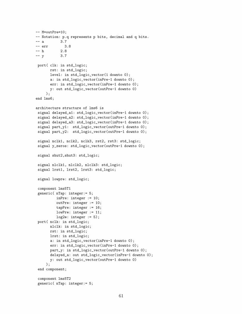
-- M=outPre=10;-- Notation: p.q represents p bits, decimal and q bits.-- a 3.7-- err 3.8-- h 2.8-- y 3.7
port( clk: in std_logic;rst: in std_logic;level: in std_logic_vector(1 downto 0);a: in std_logic_vector(inPre-1 downto 0);err: in std_logic_vector(inPre-1 downto 0);y: out std_logic_vector(outPre-1 downto 0)
);end lms6;
architecture structure of lms6 issignal delayed_a1: std_logic_vector(inPre-1 downto 0);signal delayed_a2: std_logic_vector(inPre-1 downto 0);signal delayed_a3: std_logic_vector(inPre-1 downto 0);signal part_y1: std_logic_vector(outPre-1 downto 0);signal part_y2: std_logic_vector(outPre-1 downto 0);
signal nclk1, nclk2, nclk3, rst2, rst3: std_logic;signal y_zeros: std_logic_vector(outPre-1 downto 0);
signal shut2,shut3: std_logic;
signal nlclk1, nlclk2, nlclk3: std_logic;signal lrst1, lrst2, lrst3: std_logic;
signal lowpre: std_logic;
component lms5T1generic( nTap: integer:= 5;
inPre: integer := 10;outPre: integer := 10;tapPre: integer := 16;lowPre: integer := 11;log2e: integer := 5);
port( nclk: in std_logic;nlclk: in std_logic;rst: in std_logic;lrst: in std_logic;a: in std_logic_vector(inPre-1 downto 0);err: in std_logic_vector(inPre-1 downto 0);part_y: in std_logic_vector(outPre-1 downto 0);delayed_a: out std_logic_vector(inPre-1 downto 0);y: out std_logic_vector(outPre-1 downto 0)
);end component;
component lms5T2generic( nTap: integer:= 5;
61

inPre: integer := 10;outPre: integer := 10;tapPre: integer := 16;lowPre: integer := 11;log2e: integer := 5);
port( nclk: in std_logic;nlclk: in std_logic;rst: in std_logic;lrst: in std_logic;a: in std_logic_vector(inPre-1 downto 0);err: in std_logic_vector(inPre-1 downto 0);part_y: in std_logic_vector(outPre-1 downto 0);delayed_a: out std_logic_vector(inPre-1 downto 0);y: out std_logic_vector(outPre-1 downto 0)
);end component;
component lms5T3generic( nTap: integer:= 5;
inPre: integer := 10;outPre: integer := 10;tapPre: integer := 16;lowPre: integer := 11;log2e: integer := 5);
port( nclk: in std_logic;nlclk: in std_logic;rst: in std_logic;lrst: in std_logic;a: in std_logic_vector(inPre-1 downto 0);err: in std_logic_vector(inPre-1 downto 0);delayed_a: out std_logic_vector(inPre-1 downto 0);y: out std_logic_vector(outPre-1 downto 0)
);end component;
component tapctrlport( clk: in std_logic;
rst: in std_logic;shut: in std_logic;ngclk: out std_logic;grst: out std_logic);
end component;
beginy_zeros<=conv_std_logic_vector(0,y_zeros’length);
process(level) beginif level="00" thenshut2<=’1’;shut3<=’1’;lowpre<=’1’;elsif level="01" thenshut2<=’0’;shut3<=’1’;
62

lowpre<=’1’;elsif level="10" thenshut2<=’0’;shut3<=’1’;lowpre<=’0’;elseshut2<=’0’;shut3<=’0’;lowpre<=’0’;end if;end process;
nclk1<=not clk;C2: tapctrl port map(clk=>clk, rst=>rst, shut=>shut2,
ngclk=>nclk2, grst=>rst2);C3: tapctrl port map(clk=>clk, rst=>rst, shut=>shut3,
ngclk=>nclk3, grst=>rst3);
P1: tapctrl port map(clk=>clk, rst=>rst, shut=>lowpre,ngclk=>nlclk1, grst=>lrst1);
P2: tapctrl port map(clk=>clk, rst=>rst, shut=>lowpre,ngclk=>nlclk2, grst=>lrst2);
P3: tapctrl port map(clk=>clk, rst=>rst, shut=>lowpre,ngclk=>nlclk3, grst=>lrst3);
L1: lms5T1 port map(nclk=>nclk1, nlclk=>nlclk1, rst=>rst, lrst=>lrst1,a=>a, err=>err, part_y=>part_y1, delayed_a=>delayed_a1,y=>y);
L2: lms5T2 port map(nclk=>nclk2, nlclk=>nlclk2, rst=>rst2, lrst=>lrst2,a=>delayed_a1, err=>err, part_y=>part_y2, delayed_a=>delayed_a2,y=>part_y1);
L3: lms5T3 port map(nclk=>nclk3, nlclk=>nlclk3, rst=>rst3, lrst=>lrst3,a=>delayed_a2, err=>err, delayed_a=>delayed_a3,y=>part_y2);
end structure;
A.2 Clock-gating
-- Behavorial/Structural VHDL of Scalable Fifteen Tap Adaptive LMS Filter---- A Power-scalable Digital Least Means Square Filter-- Design Using High-level Design Tools---- Thesis submitted in partial fulfillment of the requirements-- of the degree of Master of Engineering and Computer Science-- at the Massachusetts Institute of Technology---- CheeWe Ng <[email protected]>-- December 2000
63

library IEEE;use IEEE.std_logic_1164.all;use IEEE.std_logic_signed.all; -- for aldec simuse IEEE.std_logic_arith.all; -- conv routines
-- control logicentity tapctrl isport( clk: in std_logic;
rst: in std_logic;shut: in std_logic;ngclk: out std_logic;grst: out std_logic);
end tapctrl;
architecture behavior of tapctrl issignal shutn,shutp,nshut: std_logic;
beginprocess(clk,shut) beginif rising_edge(clk) thenshutp<=shut;
end if;end process;process(rst,clk,shut) beginif rst=’1’ thenshutn<=’0’;
elsif falling_edge(clk) thenshutn<=shut;
end if;end process;
grst<=(shutn and shutp) or rst;
nshut<=not shutn;
ngclk<=not(clk and nshut);end behavior;
A.3 Five-tap buiilding block
-- Behavorial/Structural VHDL of Scalable Fifteen Tap Adaptive LMS Filter---- A Power-scalable Digital Least Means Square Filter-- Design Using High-level Design Tools---- Thesis submitted in partial fulfillment of the requirements-- of the degree of Master of Engineering and Computer Science-- at the Massachusetts Institute of Technology--
64

-- CheeWe Ng <[email protected]>-- December 2000
library IEEE;use IEEE.std_logic_1164.all;use IEEE.std_logic_signed.all; -- for aldec simuse IEEE.std_logic_arith.all; -- conv routines
-- 5 tap filterentity lms5T1 isgeneric( nTap: integer:= 5;
inPre: integer := 10;outPre: integer := 10;tapPre: integer := 16;lowPre: integer := 11;log2e: integer := 5);
-- m=log2e=5-- T=tapPre=10;-- M=outPre=10;-- Notation: p.q represents p bits, decimal and q bits.-- a 3.7-- err 3.8-- h 2.8-- y 3.7
port( nclk: in std_logic;nlclk: in std_logic;rst: in std_logic;lrst: in std_logic;a: in std_logic_vector(inPre-1 downto 0);err: in std_logic_vector(inPre-1 downto 0);part_y: in std_logic_vector(outPre-1 downto 0);delayed_a: out std_logic_vector(inPre-1 downto 0);y: out std_logic_vector(outPre-1 downto 0)
);end lms5T1;
architecture behavior of lms5T1 issubtype a_type is std_logic_vector(inPre-1 downto 0);subtype err_type is std_logic_vector(inPre-1 downto 0);subtype y_type is std_logic_vector(outPre-1 downto 0);
type a_chain_type is array (0 to nTap-1) of a_type;
type tap_type is array (0 to nTap-1) of std_logic_vector(tapPre-1 downto 0);type tapupdate_type is array (0 to nTap-1) of std_logic_vector(inPre*2-1 downto 0);
type tapL_type is array (0 to nTap-1) of std_logic_vector(lowPre-1 downto 0);
type hy_type is array(0 to nTap-1) ofstd_logic_vector(tapPre+inPre-1 downto 0);
subtype shynorm_type is std_logic_vector(outPre-1 downto 0);type hynorm_type is array(0 to nTap-1) of shynorm_type;
65

type hyL_type is array(0 to nTap-1) ofstd_logic_vector(lowPre+inPre-1 downto 0);
signal achain: a_chain_type;signal tapupdate: tapupdate_type;signal tapupdatenormL, tapupdatenorm, taps, nexttaps: tap_type;
signal lerr: err_type;
signal hy: hy_type;signal hyL: hyL_type;signal hynorm: hynorm_type;
signal mulA, LmulA: a_chain_type;signal mulB : tap_type;signal LmulB: tapL_type;
begin-- for synthesis, place it outside the loopachain(0)<=a;delayed_a<=achain(nTap-1); -- delay should be in the next block
process(a,rst,nclk,achain) begin-- achain(0)<=a; -- for simulation, put it insideif rst=’1’ then -- resetga: for i in 1 to nTap-1 loopachain(i)<=conv_std_logic_vector(0,achain(i)’length);end loop ga;
elsif falling_edge(nclk) thenregachain: for i in 0 to nTap-2 loopachain(i+1)<=achain(i);end loop regachain;
end if;end process;
-- ## coefficient multiply accumulate structure ##-- multiplierif rst=’0’ thenlerr=err; -- latch err signalend if;multapup: for i in 0 to nTap-1 generatetapupdate(i)<=lerr*achain(i);
end generate multapup;
-- normalize by factor of 2^(T-2-m-14)-- tapupdate has 2*inPre bits-- tapupdatenorm has tapPre bits
-- need to sign extendtapn1: for i in 0 to nTap-1 generatetapn2: for k in 2*inPre-1+tapPre-2-log2e-14 downto 0 generatetapupdatenorm(i)(k) <=tapupdate(i)(k-tapPre+2+log2e+14);end generate tapn2;
66

tapn3: for j in tapPre-1 downto 2*inPre-1 + tapPre-2-log2e-14 +1 generatetapupdatenorm(i)(j)<=tapupdate(i)(2*inPre-1); -- sign extend
end generate tapn3;end generate tapn1;
-- tap update adder-- if lrst=’1’, low-order bits to tap update adder is zeroed --> low powerprocess(lrst,tapupdatenorm) beginif lrst=’0’ thenfor i in 0 to nTap-1 looptapupdatenormL(i)<=tapupdatenorm(i);end loop;
elsefor i in 0 to nTap-1 looptapupdatenormL(i)(tapPre-1 downto tapPre-lowPre)<=
tapupdatenorm(i)(tapPre-1 downto tapPre-lowPre);tapupdatenormL(i)(tapPre-1-lowPre downto 0)<=
conv_std_logic_vector(0,tapPre-lowPre);end loop;
end if;end process;tapupadd: for i in 0 to nTap-1 generatenexttaps(i)<=taps(i)+tapupdatenormL(i);end generate tapupadd;
-- tap update registers. asynchronous reset if rst=’1’process(rst,nclk,nexttaps) beginif rst=’1’ thengt: for i in 0 to nTap-1 looptaps(i)(tapPre-1 downto tapPre-lowPre)<=conv_std_logic_vector(0,lowPre);end loop gt;
elsif falling_edge(nclk) thenfor i in 0 to nTap-1 looptaps(i)(tapPre-1 downto tapPre-lowPre)<=nexttaps(i)(tapPre-1 downto tapPre-lowPre);
end loop;end if;end process;
-- low-order bits of tap-update registersprocess(lrst,nlclk,nexttaps) beginif lrst=’1’ thengtL: for i in 0 to nTap-1 looptaps(i)(tapPre-lowPre-1 downto 0)<=conv_std_logic_vector(0,tapPre-lowPre);end loop gtL;
elsif falling_edge(nlclk) thenfor i in 0 to nTap-1 looptaps(i)(tapPre-lowPre-1 downto 0)<=nexttaps(i)(tapPre-lowPre-1 downto 0);end loop;
end if;end process;
-- ## filter multiplier ##-- need a latch to keep bits in multiplier from glitching
67

process(achain,taps,lrst) beginif lrst=’0’ thenfor i in 0 to nTap-1 loopmulA(i)<=achain(i);mulB(i)<=taps(i);end loop;
elsefor i in 0 to nTap-1 loopLmulA(i)<=achain(i);LmulB(i)<=taps(i)(tapPre-1 downto tapPre-lowPre);end loop;
end if;end process;
tapmul: for i in 0 to nTap-1 generatehy(i)<=mulA(i)*mulB(i);hyL(i)<=LmulA(i)*LmulB(i);end generate;
-- normalize by factor of 2^(M-3-T-5)process(hy,hyL,lrst) begintapn4: for i in 0 to nTap-1 looptapn5: for k in outPre-1 downto 0 loopif lrst=’0’ thenhynorm(i)(k)<=hy(i)(k-OutPre+3+tapPre+5);
elsehynorm(i)(k)<=hyL(i)(k-OutPre+3+lowPre+5);
end if;end loop tapn5;
end loop tapn4;end process;
-- convolution sum: hyprocess(hynorm,part_y)variable partsum: shynorm_type;beginpartsum:=part_y;sumhynorm: for i in nTap-1 downto 0 looppartsum:=partsum+hynorm(i);
end loop;y<=partsum;end process;
end behavior;
68

Appendix B
Tutorial:
Using the Synthesis and
Place-and-Route Design Flow
This appendix serves as an introduction for a digital IC designer transitioning from
custom layout to automated tools. It will not cover advanced topics such as opti-
mization methods in placement and routing, and solutions to routing problems. The
reader is refered to [4, 3, 34] for more information about how to use these tools.
B.1 Basic Synthesis and Layout: An Example
The example we will use is a 4-bit adder.
B.1.1 Synthesis
The VHDL description of the example is as follows:
-- Tutorial Example for place-and-route
library IEEE;
use IEEE.std_logic_1164.all;
use IEEE.std_logic_signed.all;
69

entity example is
port( A: in std_logic_vector(3 downto 0);
B: in std_logic_vector(3 downto 0);
Y: out std_logic_vector(3 downto 0));
end example;
architecture behavior of example is
begin
Y<=A+B;
end;
Read the VHDL code into Design Analyzer. At the “Command Window” type
compile. Design Analyzer will synthesize the example using the standard-cells. When
the synthesis is complete, descend the hierarchy by clicking on the icons until you see
something like Figure B-1. Save the design as a verilog net-list.
Figure B-1: Design Analyzer.
B.1.2 Place-and-Route
The next step is to perform place-and-route with Silicon Ensemble. Change directory
to where you have the se.ini file. Run silicon ensemble by typing “seultra” at the unix
prompt.
70

Import LEF
The first step is to import the information that will tell Silicon Ensemble where the
pins of the various standard-cells are located. This file is contained in a “.lef” provided
by the cell provider. Under the “File” menu, click “Import-LEF”. A window like the
one in Figure B-2 should appear. Fill in the location of the .lef and click the “OK”
button.
Figure B-2: Silicon Ensemble Import LEF Dialog.
Once the .lef is loaded, you can save the design, so subsequently you only need to
open the design and skip the import lef step. The default design name is “LBRARY”.
Import Verilog
The next step is to import the verilog net-list from synthesis.
If you are importing for the first time, compile a verilog library for the standard
cells first by importing a verilog description of the cells provided by the standard-cell
71

provider. Figure B-3 shows the “Import-Verilog” dialog box to import the standard-
cell for the first time. Once you have done that, you can import the verilog netlist
from synthesis by specifying the name of the compiled verilog library in the “Compiled
Verilog Reference Libraries” line. Be sure to specify the “Verilog Top Module” of your
design.
Figure B-3: Silicon Ensemble Import Verilog Dialog.
Floor Planning
The next step is floor planning. Under the “Floorplan” menu, click “Initialize Floor-
plan.” Figure B-4 showns the “Initialize Floorplan” dialog box. Be sure to click “Flip
Every Other Row” and “Calculate”. Pick a comfortable “IO To Core Distance” if
you wish to make VDD and GND rings around the chip.
72

Figure B-4: Silicon Ensemble Initialize Floorplan.
73

Place IOs
Under the “Place” menu, click “IOs...”. The dialog box in Figure B-5 should appear.
Click “OK”
Figure B-5: Silicon Ensemble Place IOs.
Place Cells
Under the “Place” menu, click “Place Cells”. The dialog box in Figure B-6 should
appear. Click “OK”
Figure B-6: Silicon Ensemble Place Cells.
By this time, you should obtain in the main window something like
74

Figure B-7: Silicon Ensemble window after placement.
75

Add Filler Cells
At this point, you need to add filler cells, to fill up the empty cells. Click “Filler
Cells-Add Cells” under the “Place” menu. You can use the settings as shown in
Figure B-8
Figure B-8: Silicon Ensemble Add Filler Cells.
Plan Power
This step adds VDD and GND rings around the chip. First, pull up the menu “Route-
Plan Power”. Click Add Rings. Figure B-9 should appear. Do the necessary setting,
like shown in the figure, and click OK.
To complete this step, click “Connect Ring” under the “Route” menu and click
“OK”.
76

Figure B-9: Silicon Ensemble Add Rings.
Route
The final step is to route the entire design. Click “WRoute” under “Route” menu,
and click “OK.” When the entire design is routed, the main window should look like
the following.
Export GDSII
The final step in Silicon Ensemble is to export it to a GDSII file that will be imported
into Cadence Design Framework. Figure B-11 shows the dialog box you should pull
up from the “File-Export” menu. You will need to make a gds2.map file, if the cell
provider does not provide it. An example is shown below:
13 POLY1;
16 METAL1;
17 VIA12;
18 METAL2;
27 VIA23;
28 METAL3;
29 VIA34;
31 METAL4;
40 NAME METAL1;
77

Figure B-10: Silicon Ensemble window after routing.
Figure B-11: Silicon Ensemble Export GDSII.
78

41 NAME METAL2;
42 NAME METAL3;
43 NAME METAL4;
62 CELL;
Import Stream into Design Framework
The final step is to import the routed cell in design framework. Start design framework
with “icfb” Under the “File” menu, click “Import-Stream” to stream in the GDSII file
from Silicon Ensemble. You will need to specify the layer map and ASCII technology
file in the dialog box shown in Figure B-12 After refreshing the Library Manager, you
Figure B-12: Design Framework Stream In. Click “User-Defined Data” on the leftdialog for the right dialog to appear.
should be able to open the layout view of the cell, as shown in Figure B-13
B.2 Extraction
Running Dracula Layout Parasitic Extraction (LPE) correctly requires taking care
of subtle issues in compatibility of the netlist. The following is a shell script for
running Dracula. One important command to include in running loglvs is the “fpin”
command, because the verilog net-list Synopsys synthesizes sometimes leaves out pins
in module instantiations.
79

Figure B-13: Design Design Framework Virtuoso Layout.
80

run.sh
#! /usr/local/bin/tcsh -f
# [cell name] [verilog source]
#
# expects to find [cell name].gds2 in the folder [cell name]
# change to the directory containing [cell name].gds2
cd $1
# compiles schematic for LPE
LOGLVS << END >! loglvs.log
DXF
fpin
CIR /u/vader/cheewe/artisan/tsmc018-2000q1v3/aci/sc/lvs_netlist/tsmc18.cdl
ver $2
LINK $1
CON
EXIT
END
# makes a copy of dracLPE.rul from the parent directory, substituting
# the names of the cells
sed -e "s/_cell_name_/$1/\
s/gds/gds2/" ../dracLPE.rul >! dracLPE.rul
# compiles the LPE rules
PDRACULA << END >! pdracula.log
/get dracLPE.rul
/fin
END
# run LPE
./jxrun.com >! jxrun.log
B.3 Running Powermill
Powermill can be run on both the Verilog netlist, as well as the extracted SPICE
netlist. The Verilog netlist retains hierarchical structure, but the SPICE netlist is
flattened in the LPE process. Section C.5 describes the necessary steps to set up the
81
model files to run powermill under both situations.
Since the SPICE netlist is flattened, it is more difficult to measure the power
dissipation of sub-blocks. One of the ways is to parse the netlist and provide a unique
VDD for each sublock.
The SPICE netlist from LPE does not name the models correctly if the LVS
netlist from the cell-provider does not. In this thesis, TSMC has a different model
for different sizes of transistors. It is necessary to parse the SPICE netlist and insert
the proper model names according to the gate width.
There are some syntax differences between the SPICE output from LPE and Epic.
The LPE netlist uses VSS instead of 0, so a search and replace is needed. Synopsys
produces node names that contain “+”- which propagate through LPE. They must
be removed because they are incompatible with Epic.
The following subsections documents the scripts to perform the above functions.
DoSubVDDmodel.sh
This shell script takes the SPICE.DAT output from LPE, calls other shell-scripts to
create a unique VDD for each sub-block, and make a Epic configuration file epic.cfg
to report the power for all these VDD. vCells.sp contains the supply definitions for
the VDDs.
SubVDDmodel.sh SPICE.DAT >! LPE.sp
sort -o sCells Cells
awk -f Vlist.awk sCells >! vCells.sp
awk -f makeCfg.awk sCells >! epic.cfg
SubVDDmodel.sh
This shell script substitutes the correct model name, and creates a unique VDD for
each sub-block.
#! /usr/local/bin/tcsh -f
sed -f PreSize.sed $1 | awk -f PreModel.awk | sed -f SubModel.sed\\
82

| sed -e ’s/"+"-//g’
PreSize.sed
This Sed script prepends the gate length so that PreModel can pick out the correct
model for each transistor declaration.
# Takes a spice deck, ignores line that do not begin with M,C,+
# Substitutes {name}-VDD for VDD, 0 for VSS
# Prepends gate width
# output should be piped to PreModel.awk
#
# delete all lines that do not begin with M,C,+
/^[^MC+]/d
# append each line with a space for convenience
s/\(.*\)/\1 /
# keep a copy of lines that begin with M till NRD is found
/^M/{
h
d
}
# NRD is found, process
/NRD=/{
# append this line and get it
H
g
# search for the name of the cell and save it in a file Cells
s/^M\([^\\]*\)\\\([^ ]*\).*/_C\2/
/^_C/{
s/^_C//
w Cells
}
# get the line back, search for name of cell and prepend it
g
s/^M\([^\\]*\)\\\([^ ]*\)/\2, M\1\\\2/
# replace all VDD with {name}-VDD (at most appears twice), but keep VSS
s/\(.*\), \(.*\) VDD /\1, \2\1-VDD /
s/\(.*\), \(.*\) VDD /\1, \2\1-VDD /
# remove the name of the cell, after VDD has been replaced
s/\(.*\), //
# replace VSS with 0 (appears at most twice)
s/ VSS / 0 /
83

s/ VSS / 0 /
# prepend the gate width
s/\(.*\)W=\([0-9]*\.[0-9]*\)/\2, \1W=\2/
p
d
}
# keep a copy of lines that begin with +
/^+/{
H
d
}
# substitute VSS for C’s too
/^C/s/ VSS / 0 /
PreModel.awk
This Awk script prepends the correct spice model, given the input from PreSize.sed
# Takes the output from PreSize.sed
# and replaces the prepend with correct spice model
# Output should be piped to SubModel.sed
BEGIN { FS=","}
/^[0-9]/{
if ($1<0.6)
print "ch12"$2;
else if ($1<1.3)
print "ch9"$2;
else if ($1<10.1)
print "ch6"$2;
else
print "ch3"$2;
}
/^[^0-9]/{
print $0
}
SubModel.sed
This script takes the output from PreModel.awk and replaces the original model
names “N” and “P” with the correct one.
84

# Takes the output from PreModel.awk
# replaces N and P with the correct string
#
# delete all lines that do not begin with c,C,+
/^[^cC+]/d
# keep a copy of lines that begin with n,p till NRD is found
/^[c]/{
h
d
}
# NRD is found, process
/NRD=/{
# append this line and get it
H
g
# substitute P or N of ’ N ’ or ’ P ’ is found, and remove prepend
s/^c\([^ ]*\) \(.*\) N \(.*\)/\2 nc\1 \3/
s/^c\([^ ]*\) \(.*\) P \(.*\)/\2 pc\1 \3/
# substitute P or N of ’ N\n’ or ’ P\n’ is found, and remove prepend
s/^c\([^ ]*\) \(.*\) N\n/\2 nc\1\
/
s/^c\([^ ]*\) \(.*\) P\n/\2 pc\1\
/
}
# keep a copy of lines that begin with +
/^+/{
H
d
}
Vlist.awk
This Awk scripts creates the supply declarations of VDDs
BEGIN {OFS=" "}
$1 != LastCell {
LastCell = $1
print "V"$1, $1"-VDD", 0, "pVdd"
}
85

makeCfg.awk
This script creates the Epic configuration file to measure the power supplied by each
VDD.
BEGIN {OFS=""; ORS=""; x=1}
$1 != LastCell {
if (x%10==1) print "report_node_powr"
LastCell = $1
print " ",$1,"-VDD"
if (x%10==0) print "\n"
x=x+1
}
END { print "report_node_powr VDD CLK A[* ERR[* Y[*\n" }
86

Appendix C
Tutorial:
Setting Up the Synthesis and
Place-and-Route Design Flow
This appendix describes the process of setting up a digital design flow involving Syn-
opsys Design Analyzer, Cadence Silicon Ensemble, Cadence Design Framework II,
Cadence Dracula, and EPIC Powermill. It does not cover setting up the shell envi-
ronment variables, such as PATH, LICENSE FILE, etc., to run these tools. Rather
it will describe the steps you need to do to set up the flow after the tools can be run.
You will need to ask the system admin of the lab to set up the tools itself. At the
writing of this thesis, the versions of the tools are shown in Table C.1
Table C.1: Versions of CAD toolsTool VersionDesign Analyzer 1999.10Silicon Ensemble 5.3Design Framework 4.45Powermill 5.4
87

Table C.2: Data Files Required for CAD ToolsTool Data Files SourceDesign Analyzer *.db, *.lib ArtisanSilicon Ensemble *.lef Artisan
*.tlf (optional) Artisana Verilog definition of the cells Artisangds2.map Artisan,
or create your ownDesign Framework front-end cell-views in GDSII Artisan
layer map, font map (optional) TSMCdisplay.drf, ASCII technology file TSMC
Dracula Dracula DRC or LPE rules TSMCLVS netlist of standard cells Artisan
Powermill SPICE models TSMCLVS netlist of standard cells Artisan
C.1 Data files for CAD Tools
You will need to obtain several data files pertaining to the particular fabrication
process and cell library, from the respective foundry and the library provider. In
this thesis, we used Taiwan Semiconductor Manufacturing Co., Ltd. (TSMC) and
Artistan Components, Inc.
C.2 Setting Up Design Analyzer
To set up designer analyzer to use the back-end views of your standard-cells and
DesignWare for synthesis you need to add or modify the following lines in the .syn-
opsys dc.setup file located in the start-up directory of “design analyzer”
search_path= search_path + ‘‘path containing *.db and *.lib’’
target_library=typical.db
symbol_library=typical.db
synthetic_library=dw_foundation.sldb
link_library={typical.db, dw_foundation.sldb}
synlib_wait_for_design_license={"DesignWare-Foundation"}
Here “typical.db” is the back-end library provided by Artisan Components.
88

C.3 Setting Up Cadence Silicon Ensemble
The cell provider may specify certain enviroment variables to be set in the “se.ini” file
in the start-up directory of “seultra.” For example, the following lines were provided
by Artisan Components for the TSMC 0.18 SAGE-X standard cell library:
# Silicon Ensemble floorplan variables - required for TSMC .18
set v plan.rgrid.M1offset 560 ;
set v plan.rgrid.M2offset 660 ;
set v plan.rgrid.M3offset 560 ;
set v groute.Allow.OffGrid.PinAccess false ;
set v froute.Allow.OffGrid.PinAccess false ;
set v froute.Avoid.OffGrid.Blockage true ;
set v froute.Build.OffGrid.SPins false ;
In addition, I found it necessary to add the following line. The verilog output
from design analyzer uses “[]” as parenthesis, while the default for Silicon Ensemble
is “()”. It is crucial that they are the same, because in the Layout-versus-schematics
step, the layout will be compared to the verilog netlist.
# so that pins are labeled with [] which is compatible with spice and verilog
SET VAR INPUT.VERILOG.BUS.DELIM "[]" ;
C.4 Setting up Design Framework
In order for design framework to incorporate the front-end cell-views into the place-
and-routed view from Silicon Ensemble, the front-end cell-views must be imported
into Design Framework.
To do so, create a new library using the “Library Manager” specifying the directory
to contain the new library. Then import the GDSII file containing the front-end views,
specifying the technology file, the layer map and font map files. After completion,
fire up Virtuoso by opening one of the layouts, pull up the “Display Resource Editor”
menu under “LSW” as shown in Figure C-1 and load the new display.drf file.
89

Figure C-1: Setting up display.drf.
C.5 Setting up Powermill
Powermill requires the SPICE models for the transistors. In some cases, you need
to do a search-and-replace for syntax differences between the SPICE models given
by the foundry and the acceptable by Powermill. In TSMC’s model, it uses “nch.6”
to “nch.12” and “pch.6” to “pch.12” as model names. “.” is not acceptable in the
syntax for Epic and must be removed.
Powermill can also be used to perform rough power estimation using the Verilog
netlist obtained from synthesis. To do so, you need to compile the LVS netlist from
the cell-provider into the Epic proprietary netlist format using “vlog2e”. Since the
LVS netlist does not specify the correct model for the gate width, I replaced all the
references to the model “n” with “nch9” and all the references to “p” with “pch9”.
The LVS netlist uses “VSS” as ground node, so you will need to replace “VSS” with
“GND”.
90

Bibliography
[1] Kamran Azadet and Chris J. Nicole. Low-Power Equalizer Architectures for
High-Speed Modems. IEEE Communications Magazine, pages 118–126, October
1998.
[2] John A. C. Bingam. The Theory and Practice of Modem Design. John Wiley &
Sons, 1988.
[3] Cadence. Envisia Silicon Ensemble Place-and-Route Reference.
[4] Cadence. Virtuoso Layout Editor User Guide.
[5] Anantha P. Chandrakasan and Robert W. Broderson. Minimizing Power Con-
sumption in Digital CMOS Circuits. Proceedings of the IEEE, 83(4):498–523,
April 1995.
[6] Anantha P. Chandrakasan, Miodrag Potkonjak, Renu Mehra, Jan Rabaey, and
Robert W. Broderson. Optimizing Power Using Transformations. IEEE Transac-
tions on Computer-Aided Design of Integrated Circuits and Systems, 14(1):12–31,
January 1995.
[7] Tian-Sheuan Chang and Chein-Wei Jen. Low-Power FIR Filter Realization with
Differential Cofficients and Input. In Proceedings of 1998 IEEE International
Conference on Acoustics, Speech and Signal Processing, volume 5, pages 3009–
3012, 1998.
[8] Jr. Earl E. Swartzlander, editor. Computer Arithmetic. IEEE Computer Society
Press, 1990.
91

[9] William L. Freiking and Keshab K. Parhi. Low-power FIR Digital Filters Using
Residue Arithmetic. In Conference Record of the Thirty-First Asilomar Confer-
ence on Signals, Systems and Computers, volume 1, pages 739–741, 1998.
[10] R.D. Gitlin, H.C. Meadors Jr., and S.B. Weinstein. The Tap-Leakage Algorithm:
An Algorithm for the Stable Operation of a Digitally Implemented, Fractionally
Spaced Adaptive Equalizer. The Bell System Technical Journal, 61(8):1817–1839,
October 1982.
[11] R.D. Gitlin and S.B. Weinstein. On the Required Tap-Weight Precision for Dig-
itally Implemented, Adaptive, Mean-Squared Equalizer. Bell System Technical
Journal, 58(2):301–321, February 1979.
[12] R.D. Gitlin and S.b. Weistein. Fractionally-Spaced Equalization: An Improved
Digital Transversal Equalizer. The Bell System Technical Journal, 60(2):275–296,
February 1981.
[13] D.N. Godard. Self-Recovering Equalization and Carrier Tracking in Two-
Dimensional Data Communication Systems. IEEE Transactions on Commu-
nications, 28(11):1867–1875, November 1980.
[14] M. Goel and N.R. Shanbag. Low-Power Equalizers for 51.84 Mb/s Very-High-
Speed Digital Subscriber Loop (VDSL) Modems. In 1998 IEEE Workshop Signal
Processing Systems, pages 317–326, October 1998.
[15] Vadim Gutnik and Anantha P. Chandrakasan. Embedded Power Supply for
Low-Power DSP. IEEE Transactions on Very Large Scale Integration (VLSI)
Systems, 5(4):425–435, December 1997.
[16] Simon S. Haykin. Adaptive Filter Theory. Prentice-Hall, 1996.
[17] Henry Samueli Jeffey S. Putnam. A 4-Channel Diversity QAM Receiver for
Broadband Wireless Communications. In 1999 IEEE International Solid-State
Circuits Conference, pages 338–9, 1999.
92

[18] Curtis A. Siller Jr. and Walter Debus. Decision-Directed Fractionally Spaced
Equalizer Control Using Time-Domain Interpolation. IEEE Transactions on
Communications, 39(2), February 1991.
[19] G. Karam, P. Moreau, and H. Sari. Stabilizing Fractionally-Spaced Equalizers.
In GLOBECOMM ’91 Conference Record, pages 51.4.1–5, 1991.
[20] Fang Lu and Henry Samueli. A 60-Mbd, 480-Mb/s, 256-QAM Decision-Feedback
Equalizer in 1.2-µm CMOS. IEEE Journal of Solid-State Circuits, 28(3):330–338,
March 1993.
[21] R.W. Lucky. Signal Filtering with the Transversal Equalizer. In Proceedings 7th
Annual Allerton Conference on Circuits and Systems Theory, pages 792–804,
October 1969.
[22] Jeffrey T. Ludwig, S. Hamid Nawab, and Anantha P. Chandrakasan. Low-Power
Digital Filtering Using Approximate Processing. IEEE Journal of Solid-State
Circuits, 31(3):395–400, March 1996.
[23] Manesh Mehendale, S.D. Sherlekar, and G. Venkatesh. Algorithmic and Architec-
tural Transformations for Low Power Realization of FIR Filters. In Proceedings
of 1998 Eleventh International Conference on VLSI Design, pages 12–17, 1998.
[24] S. Hamid Nawab, Alan V. Oppenheim, Anantha P. Chandrakasan, Joseph M.
Winograd, and Jeffrey T. Ludwig. Approximate Signal Processing. Journal of
VLSI Signal Processing, 15:177–200, 1997.
[25] Chris J. Nicol and Patrik Larsson. Low Power Multiplication for FIR Filters. In
Proceedings IEEE International Sympossium Low Power Electronics and Design,
pages 76–79, August 1997.
[26] Chris J. Nicol, Patrik Larsson, Kamran Azadet, and Jay H. O’Neill. A Low-Power
128-Tap Digital Adaptive Equalizer for Broadband Modems. IEEE Journal of
Solid-State Circuits, 32(11):1777–1789, November 1997.
93

[27] C.J. Nicol P. Larsson. Self-Adjusting Bit-Precision for Low-Power digital Filters.
In 1997 Symposium on VLSI Circuit Digest of Technical Papers, pages 123–124,
1997.
[28] Darren N. Pearson and Keshab K. Parhi. Low-Power FIR Digital Filter Ar-
chitectures. In 1995 IEEE International Sympossium on Circuits and Systems,
volume 1, pages 231–234, 1995.
[29] John G. Proakis. Digital Communications. McGraw-Hill Book Company, 1983.
[30] S.U.H Qureshi. Adaptive Equalization. In Proceedings IEEE, volume 73, pages
1349–1387, September 1985.
[31] U.H. Shahid and J.r G. David Forney. Performance and Properties of T/2 Equal-
izer. In National Telecommunications Conference, pages 11:1–1–11:1–8, Decem-
ber 1977.
[32] Naresh R. Shanbag and Manish Goel. Low-Power Adaptive Filter Architectures
and Their Application to 51.84 Mb/s ATM-LAN. IEEE Transactions on Signal
Processing, 45(5), May 1997.
[33] Amit Sinha and Anantha P. Chandrakasan. Energy Efficient Filtering Using
Adaptive Precision and Variable Voltage. In Proceedings of Twelfth Annual IEEE
ASIC/SOC Conference 1999, pages 327–331, September 1999.
[34] Synopsys. Synopsys Online Documentation.
[35] Loke Kun Tan, Jeffrey S. Putnam, Fang Lu, Lionel J. D’Luna Dean W. Muelle,
Kenneth R. Kindsfater, Keller B. Cameron, Rboindra B. Joshi, Robert A. Haw-
ley, and Henry Samueli. A 70-Mb/s Variable-Rate 1024-QAM Cable Receiver
IC with Integrated 10-b ADC and FEC Decoder. IEEE Journal of Solid-State
Circuits, 33(12):2205–2217, December 1998.
[36] J.R. Treichler, I. Fijalkov, and C.R. Johnson Jr. Fractionally Spaced Equalizers.
IEEE Signal Processing Magazine, May 1996.
94

[37] Tomohiko Uyematsu and Kohichi Sakaniwa. A New Tap-adjustment Algorithm
for the Fractionally Spaced Equalizer. In GLOBECOM’85 Conference Record,
pages 46.3.1–4, 1985.
[38] Alice Wang, Wendi Rabiner Heinzelman, and Anantha P. Chandrakasan. Energy-
Scalable Protocols for Battery-Operated MicroSensor Networks. In Proceedings
of 1999 IEEE Workshop on Signal Processing Systems, pages 483–492, 1999.
[39] Meng-Lin Yu and Patrik Larson. A Technique for Improving the convergence
Probability of Blind Equalizers. In International Conference on Information,
Communications and Signal Processing ’97, September 1997.
95


![Assisting with Scalable Scalable Vector Graphics and ... · SVG Scalable Vector Graphics [6] SSVG Scalable Scalable Vector Graphics [10] LWA Live Website Annotate [See Section 4]](https://img.pdfslide.net/doc/110x75/5fdccc690a10ab2c1e74ae97/assisting-with-scalable-scalable-vector-graphics-and-svg-scalable-vector-graphics.jpg)